

Page 1
V1.0
1
TBMDA2
Modulated Wideband Driver Amplifier
1 Introduction
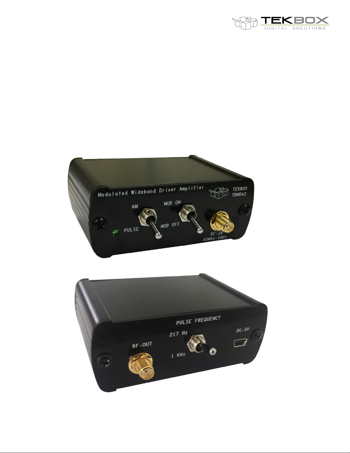
The TBMDA2 modulated wideband driver amplifier is designed in order to create an inexpensive signal source
for immunity testing of electronic building blocks and products. It is designed to be driven by the tracking
generator output of spectrum analyzers. With its 1dB compression point of +27dBm, it can boost the output
power of a tracking generator up to 500mW. The TBMDA2 is ideal to drive Tekbox near field probes in order to
find the sensitive spot of an electronic circuit or to create electric fields up to 170V/m when driving the Tekbox
TEM Cell TBTC0, 100V/m when driving the TBTC1, 50V/m when driving the TBTC2 or 30V/m when driving the
TBTC3. Test signals for immunity testing can be CW, AM or PM. Consequently, the TBMDA2 provides built in
modulation capability to generate 1 kHz AM or PM signals. In PM mode, the TBMDA2 can also generate a 217
Hz Signal with 12.5% duty cycle in order to simulate mobile phone TDMA noise.
Picture 1 – TBMDA2 modulated wideband driver amplifier, front view
Picture 2 – TBMDA2 modulated wideband driver amplifier, rear view
Page 2
V1.0
2
10 MHz
25 MHz
100 MHz
200 MHz
300 MHz
400 MHz
500 MHz
600 MHz
700 MHz
44.2 dB
46.3 dB
46.7 dB
46.6 dB
45.3 dB
44.2 dB
43.8 dB
42.9 dB
41.7 dB
800 MHz
900 MHz
1 GHz
1.1 GHz
1.2 GHz
1.3 GHz
1.4 GHz
1.5 GHz
39.6 dB
40.1 dB
39.3 dB
38.5 dB
37.3 dB
36.8 dB
35.9 dB
34.8 dB
TBMDA2
Modulated Wideband Driver Amplifier
Application:
General-purpose gain block
Signal source for immunity testing, driving near field probes
Signal source for immunity testing, driving TEM Cells
Features:
CW amplifier (modulation off)
1 kHz, 80% AM modulation
1 kHz, 50% duty cycle pulse modulation
217 Hz, 12.5% duty cycle pulse modulation
2 Electrical Specifications
Technical Data:
Input / Output: 50 Ohm, SMA female
Nominal supply Voltage: 5V, typ. 700mA, Mini-USB-B connector
Maximum supply voltage: 5.5V
Maximum input power: -8dBm continuous, 0 dBm @ 25°C for 5 minutes max.
Operating temperature range: -20°C to 50°C
Frequency range: 10MHz – 1.5 GHz
1dB output compression point @ 10MHz: +24 dBm typ.
1dB output compression point @ 100 MHz: +27 dBm typ.
1dB output compression point @ 1 GHz: +27 dBm typ.
1dB output compression point @ 1.5 GHz: +26.5 dBm typ.
Harmonics: < - 30 dBc typ.
Internal modulation frequency AM: 1 kHz ±10%
Internal modulation frequencies PM: 1 kHz ±10%, 217 Hz ±20%
Duty cycle, PM: 50% ±10% @ 1 kHz; 12.5% ±20% @ 217 Hz
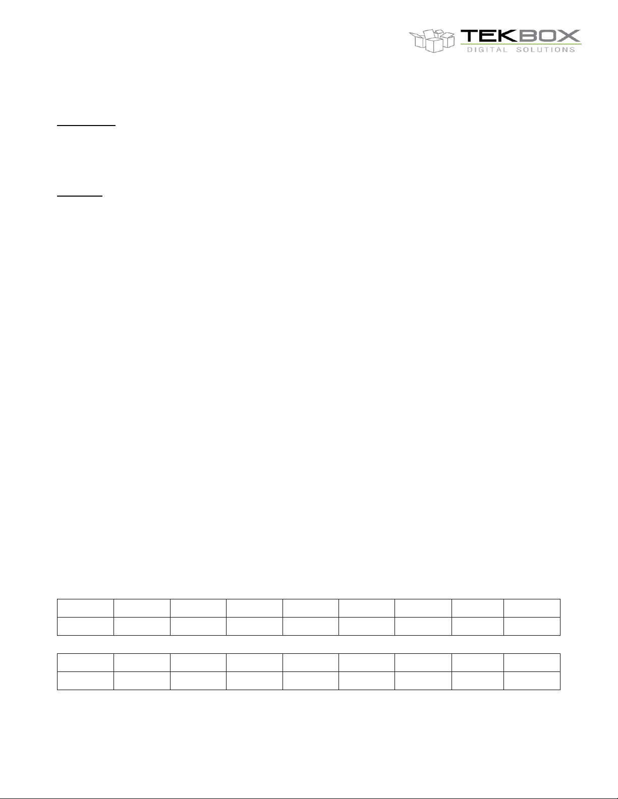
Gain:
Table 1 – TBMDA2 gain
Page 3
V1.0
3
Frequency
[MHz]
Output power
@ -20 dBm input
power [dBm]
Output power
@ -18 dBm input
power [dBm]
Output power
@ -16 dBm input
power [dBm]
Output power
@ -14 dBm input
power [dBm]
Output power
@ -12 dBm input
power [dBm]
Output power
@ -10 dBm input
power [dBm]
Output power
@ -8 dBm input
power [dBm]
10
24.8
24.8
24.8
24.7
24.4
24.1
24.3
25
26.4
26.4
26.1
25.7
25.4
25.5
25.7
50
27.1
27.2
26.9
26.5
26.2
26.2
26.4
100
27.1
27.6
27.5
27.2
26.7
26.7
27
200
26.7
27.8
27.9
27.6
27.2
27.2
27.2
300
26.1
27.5
27.8
27.6
27.4
27.2
27.2
400
25.6
27.4
28.2
28.1
27.8
27.4
27.4
500
24.9
26.7
28
28.2
28
27.7
27.5
600
24.1
26.1
27.6
28.2
28.2
27.8
27.6
700
23
24.9
26.6
27.6
27.8
27.6
27.3
800
20.9
22.8
24.6
26.1
26.6
26.5
26.5
900
21.2
23.2
25.1
26.8
27.9
28.1
28.1
1000
20.5
22.5
24.4
26.2
27.6
28.1
28.1
1100
19.5
21.5
23.5
25.3
27
28
28.1
1200
18.1
20.2
22.2
24.1
25.9
27.4
27.9
1300
17.7
19.7
21.7
23.7
25.5
27.2
28.1
1400
16.8
18.8
20.8
22.8
24.6
26.5
27.8
1500
15.8
17.8
19.8
21.8
23.7
25.4
27.02
0
2
4
6
8
10
12
14
16
18
20
22
24
26
28
30
0 100 200 300 400 500 600 700 800 900 1000 1100 1200 1300 1400 1500 1600
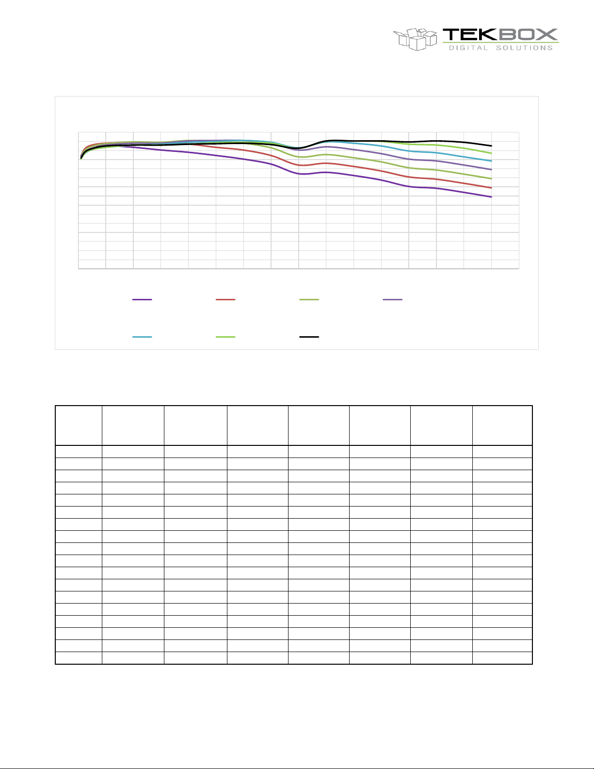
Output power versus frequency
Output power
@ -20 dBm input
power [dBm]
Output power
@ -18 dBm input
power [dBm]
Output power
@ -16 dBm input
power [dBm]
Output power
@ -14 dBm input
power [dBm]
Output power
Output power
Output power
TBMDA2
Modulated Wideband Driver Amplifier
Figure 1 – TBMDA2, output power versus frequency, 10MHz – 1.5GHz
Table 2 – TBMDA2 power table
Page 4
V1.0
4
Frequency [MHz]
Input power [dBm]
Output power [dBm]
gain [dB]
10
-19.92
24.3
44.22
25
-19.8
26.5
46.3
50
-19.6
27.1
46.7
100
-19.2
27.4
46.6
200
-18.4
27.6
46
300
-17.6
27.7
45.3
400
-16.8
27.4
44.2
500
-16
27.8
43.8
600
-15.2
27.7
42.9
700
-14.4
27.3
41.7
800
-13.6
26
39.6
900
-12.8
27.3
40.1
1000
-12
27.3
39.3
1100
-11.2
27.3
38.5
1200
-10.4
26.9
37.3
1300
-9.6
27.2
36.8
1400
-8.8
27.1
35.9
1500
-8
26.8
34.8
15
17
19
21
23
25
27
29
0 100 200 300 400 500 600 700 800 900 1000 1100 1200 1300 1400 1500 1600
Output power [dBm]
TBMDA2
Modulated Wideband Driver Amplifier
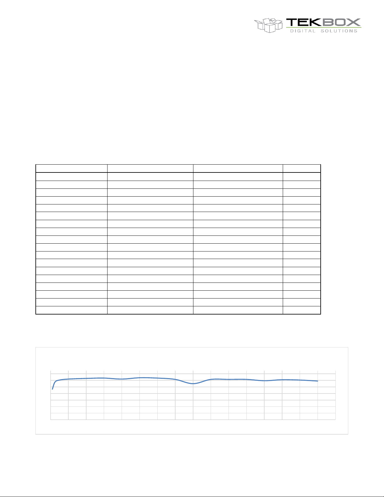
Frequency response:
The tables above show a 10dB gain variation across the frequency range 10 MHz to 1.5 GHz. When driving the
TBMDA2 with the tracking generator of a spectrum analyzer, the TG level can be set to -8 …-12 dBm to get a flat
output power response over the frequency range. This will drive the amplifier into compression for lower
frequencies. This is acceptable when using CW or pulse modulation for immunity testing. However, when doing
immunity tests with an AM modulated signal, it would clip the AM envelope, as the modulator is in front of the
output stage of the TBMDA2.
Hence, when using AM modulation, the input power shall be set to levels where the TBMDA2 is in linear operation.
Linear operation:
You can calculate the drive levels for linear operation using following approximation formula or the table below:
P
[dBm] = 0.008 *frequency [MHz]-20
input
Table 3 – input drive levels for linear operation
As tracking generator levels usually can only be adjusted in 1dB steps, apply the closest integer value.
Figure 2 – output power, applying the drive levels given in table3, 10MHz – 1.5GHz
Page 5
V1.0
5
TBMDA2
Modulated Wideband Driver Amplifier
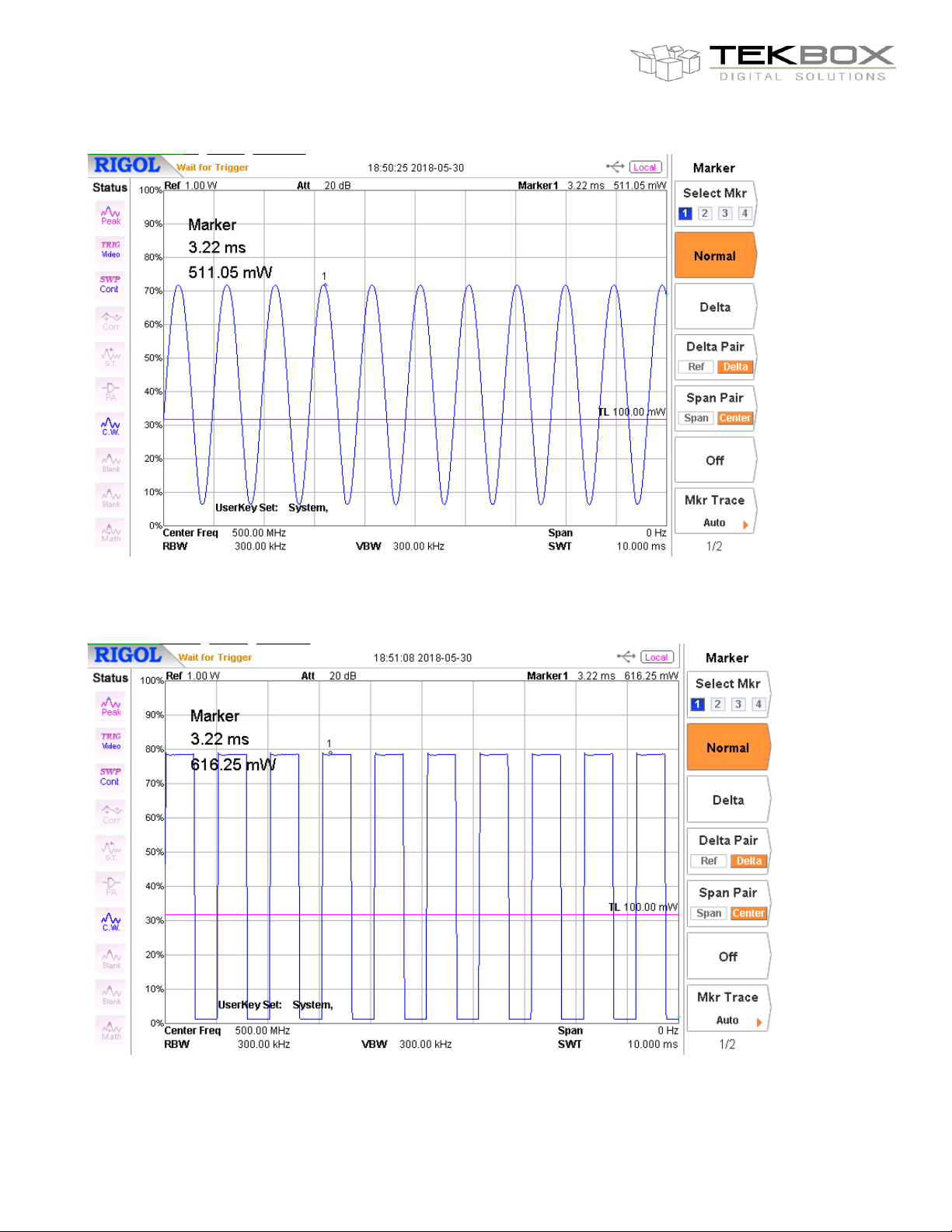
Figure 3 – 1 kHz, 80 % AM envelope, applying the drive levels given in table3, 500 MHz
Figure 4 – 1 kHz, 50 % PM envelope, 500 MHz
Page 6
V1.0
6
TBMDA2
Modulated Wideband Driver Amplifier
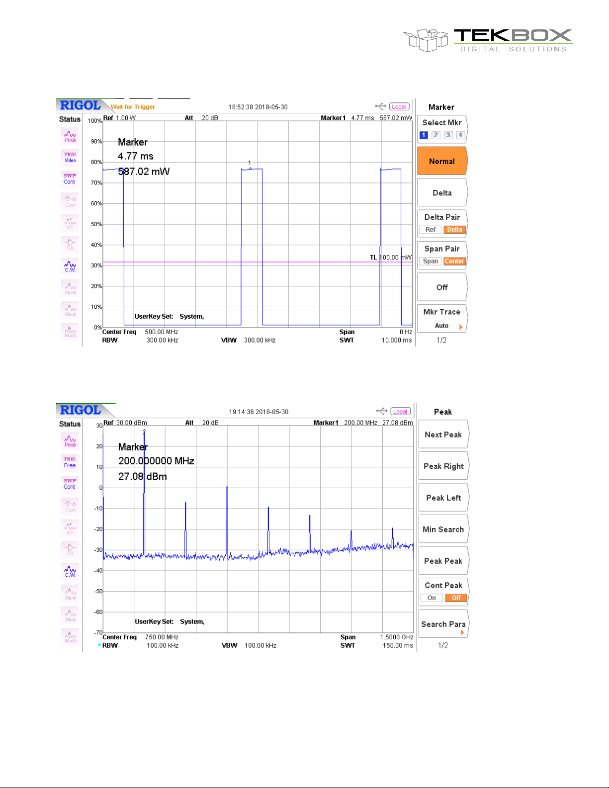
Figure 5 – 217 Hz, 12.5 % PM envelope, 500 MHz
Figure 6 – CW, harmonics, 200 MHz
Page 7
V1.0
7
TBMDA2
Modulated Wideband Driver Amplifier
3 Power supply
The current consumption of the TBMDA2 is 700mA and consequently exceeds the current limit of USB 2.0 ports.
Supply the TBMDA2 through a USB 3.0 port or a mobile phone charger with an output current capability of 1A or
higher.
Connector: Mini-USB-B
4 Applications
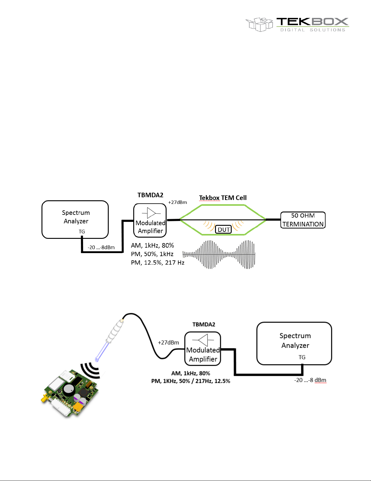
Immunity testing using a TEM cell
Figure 7 – immunity testing set up
Immunity testing using near field probes
Figure 8 – immunity testing set up
Page 8
V1.0
8
Frequency [MHz]
Input power
[dBm]
Output power
[dBm]
Field strength
TBTC0 [V/m]
Field strength
TBTC1 [V/m]
Field strength
TBTC2 [V/m]
Field strength
TBTC3 [V/m]
10
-19.92
24.3
131
73
37
24
25
-19.8
26.5
169
95
47
31
50
-19.6
27.1
181
101
51
34
100
-19.2
27.4
187
105
52
35
200
-18.4
27.6
191
107
54
36
300
-17.6
27.7
194
109
54
36
400
-16.8
27.4
187
105
52
35
500
-16
27.8
196
110
55
37
600
-15.2
27.7
194
109
54
36
700
-14.4
27.3
185
104
52
35
800
-13.6
26
159
89
45
n.a
900
-12.8
27.3
185
104
52
n.a
1000
-12
27.3
185
104
52
n.a
1100
-11.2
27.3
185
104
52
n.a
1200
-10.4
26.9
177
99
49
n.a
1300
-9.6
27.2
183
102
51
n.a
1400
-8.8
27.1
181
101
51
n.a
1500
-8
26.8
175
98
49
n.a
TBMDA2
Modulated Wideband Driver Amplifier
5 TEM Cell field strength
A typical pre compliance set up for immunity testing is typically not sophisticated enough to measure the real field
strength inside the TEM cell. However, the field strength can be approximated mathematically.
The E-field (V/m) between septum and lower (upper) wall of a TEM cell is E = V/d where V is the RMS voltage of
the applied signal and d is the distance between septum and lower (upper) wall. This is based on the simplified
assumption that the E field would be perfectly homogenous/evenly distributed. A more practical formula is E =
V*Cor/d where Cor is a correction factor for the average field strength over the volume of the DUT derived from
the analysis of the field distribution over the cross section of the cell.
Assuming the DUT is placed in the center of the cell and in the middle between bottom wall and septum, we can
however use the simplified formula with sufficient accuracy.
TBTC0: d = 2.8 cm -> E
TBTC1: d = 5 cm -> E
TBTC2: d = 10 cm -> E
TBTC3: d = 15 cm -> E
The power P in the formulas above hast to be entered in [Watt]
P
= 0.001*(10^ (P
[W]
[dBm]
= (√(P*50Ω))*35.7
[V/m]
= (√(P*50Ω))*20
[V/m]
= (√(P*50Ω))*10
[V/m]
= (√(P*50Ω))*6.66
[V/m]
/10))
Table 4 – calculated field strength for TBMDA2 driving Tekbox TEM cells
Page 9
V1.0
9
TBMDA2
Modulated Wideband Driver Amplifier
6 PC Software for immunity testing
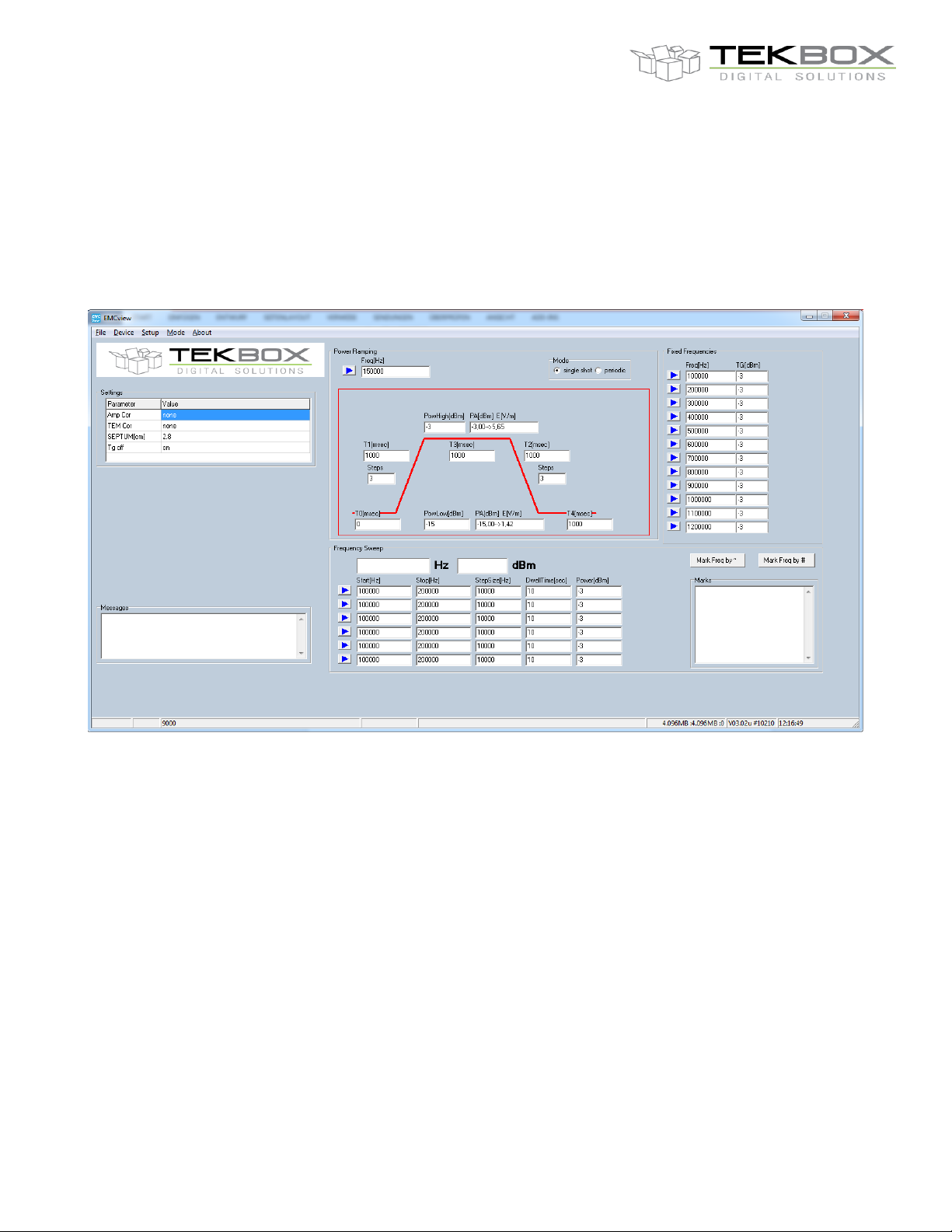
The Tekbox EMCview SW is regularly updated and now supports immunity testing with a feature for automated
tracking generator control. This significantly simplifies immunity testing, especially in case of repeated testing
during validation of DUT modifications/improvements.
Tekbox EMCview currently supports Rigol, Siglent, R&S FPC and FPH series spectrum analyzers.
Figure 9 – screenshot of the tracking generator control feature of EMCview
WARNING:
Never connect the output of the TBMDA2 directly to the input of a
spectrum analyzer. Check the maximum input ratings of the
spectrum analyzer and protect it with an appropriate attenuator.
Example:
Rigol DSA815 – maximum input power rating: +20dBm
Page 10
V1.0
10
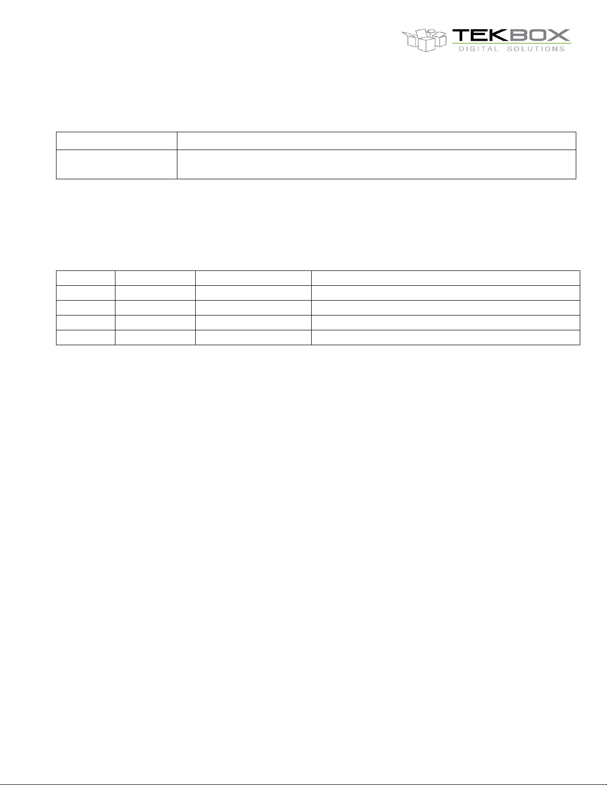
Part Number
Description
TBMDA2
modulated driver amplifier, 2 pcs 75cm SMA-male to N-male cables, 1 pc 20dB attenuator
with N-connectors, USB cable,
Version
Date
Author
Changes
V1.0
31.5.2018
Mayerhofer
Creation of the document
TBMDA2
Modulated Wideband Driver Amplifier
7 Ordering Information
8 History
Table 5 – Ordering Information
Table 6 – History
 Loading...