

Page 1
V1.0
TBBT01
Bias-Tee, 5 kHz – 1.2 GHz, 5 - 10A
1
1 Introduction
The TBBT01 Bias-Tee is a device for measuring the saturation effects of power inductors and bias voltage
effects on capacitors. The majority of available Bias-Tees for power inductor testing operate at low frequencies,
rendering them unsuitable for evaluating decoupling/bias inductors of RF power amplifiers or EMC filters.
However, RF Bias-Tees usually have restricted current capabilities and cannot be employed in the lower
frequency region. The TBBT01 can measure high bandwidth as well as high current.
Power inductors are subject to magnetic saturation effects since they often have ferrite cores. Even before
reaching the magnetic saturation current specified in inductor data sheets, the inductance begins to decrease
and the RF properties of the component degenerate.
The effect of DC current is frequently underestimated while building EMC filters, and the filter fails to work as
planned. High current Bias-Tees for current injection are required to assess the frequency response of an EMCfilter under load conditions.
High current bias tees can be used for a wide range of additional applications. Wherever inductors are used for
decoupling and filtering in DC paths, it is best procedure to measure inductance under load current conditions.
The same holds true for bias current-carrying pulse transformers.
The TBBT01 can inject up to 10A DC current into a 50 Ohm RF-path and operates at frequencies between 5 kHz
and 1.5 GHz.
The TBBT01's insertion loss is unrelated to injection current.
Page 2
V1.0
TBBT01
Bias-Tee, 5 kHz – 1.2 GHz, 5 - 10A
2
2 Parameters
Usable frequency range: 5 kHz – 1.2 GHz
RF path insertion loss: <1 dB typ. in the range 10 kHz – 1 GHz
< 1.5 dB in the range 5 kHz – 1.2 GHz
VSWR: 1 < VSWR < 2 in the range 5 kHz to 1 GHz
Characterized frequency range: 1 kHz -3 GHz
RF power handling: 50 W from 5 kHz – 1 GHz
RF- connectors: N-female
Operating voltage range: max. ±100 V;
Operating current range: ± 5A to 10 A DC; see heat up characteristics plot
± 5A DC continuous
max. ± 15 A DC
DC path resistance: < 1.5 Ω @ 22°C
DC input socket: Phoenix Contact 1998933, male
mating female terminal: Phoenix Contact 1967375
Dimensions: 150 mm x 155 mm x 330 mm;
Weight: 3 kg
3 Insertion loss
TBBT01, Insertion Loss, 1 kHz – 3 GHz
Page 3
V1.0
TBBT01
Bias-Tee, 5 kHz – 1.2 GHz, 5 - 10A
3
4 Principle schematic
Simplified schematic of the TBBT01
5 Protection
Bias-Tees serve as a protective barrier between delicate test equipment and high voltage or high
current sources. It is critical to comprehend any potential risks related to its operation.
There are three probable sources of high voltage spikes on the RF path:
1) The TBBT01 bias path contains high inductance chokes, which could create flyback voltage
spikes. As a result, the Bias Tee is designed with transient suppressors fitted across the choke
terminals.
2) When operating the device at high voltages, the coupling capacitor potentially could inject high
voltage into the RF-path. This could be avoided by connecting a transient suppressor between
RF path and ground. However, suppressors with a short turn on time and low capacitance are
susceptible to high energy pulses and tend to short out, necessitating Bias-Tee repair.
Furthermore, the Bias-Tee could not handle high RF power with such suppressors in place. As
a result, the RF path of the TBBT01 is not equipped with any transient suppressors. Thus,
avoid rapidly switching high external supply voltages on and off.
Always increase or decrease the bias voltage or current gradually. Don´t turn it
rapidly on/off.
Alternatively, use limiters or attenuators to protect the RF ports of the attached test equipment.
One more option is to install transient suppressors on the external component test PCB.
3) When measuring high inductance power inductors, rapid changes in bias current can create
flyback transients directly on the RF path. As the RF ports are not protected from potential
flyback pulses of the inductor under test, Tekbox supplies test PCBs equipped with RF
transzorbers. If you make your own test PCBs, add appropriate transzorbers or ramp the
current up/down gently instead of turning it on/off quickly.
Page 4
V1.0
TBBT01
Bias-Tee, 5 kHz – 1.2 GHz, 5 - 10A
4
6 Thermal characteristics
Coil temperature vs. current
Limit the measurement time to keep the coil temperature below 125°C
7 VSWR
VSWR; Port RF, PORT RF+DC
0
10
20
30
40
50
60
70
80
90
100
110
120
130
0 10 20 30 40 50 60 70 80
[°C]
[minutes]
TBBT01 heat-up characteristics
5A 6A 7A 8A 9A 10A
Page 5
V1.0
TBBT01
Bias-Tee, 5 kHz – 1.2 GHz, 5 - 10A
5
8 Application examples
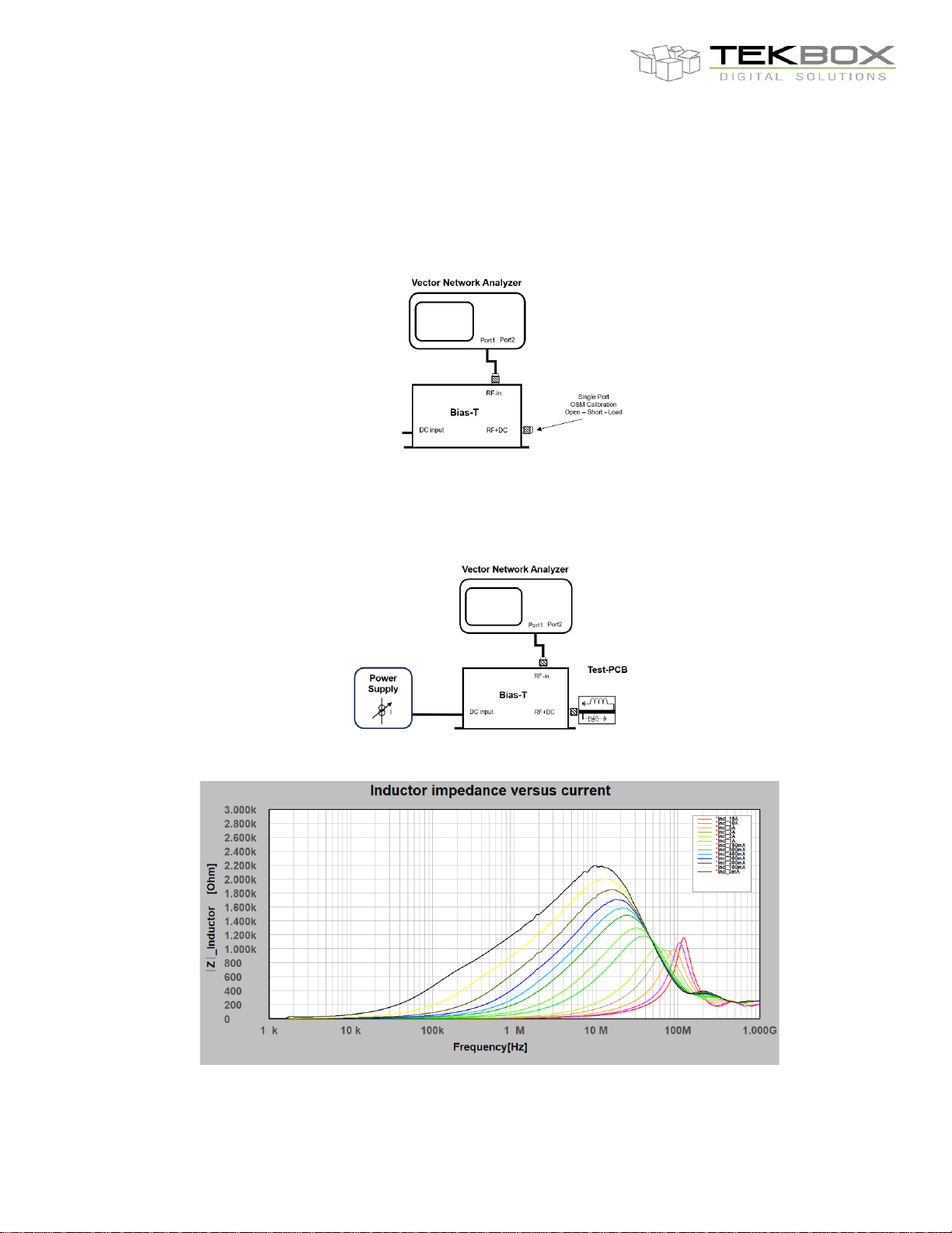
8.1 Inductor impedance vs. frequency and current
1) Connect a Vector Network Analyzer to the RF-port of the Bias-Tee. Carry out an OSL calibration at the
RF+DC - port of the Bias-Tee.
Calibration setup
2) Connect a test PCB with the inductor to the RF+DC port. Depending on coaxial couplers and the length of
the PCB, you may enter a suitable electrical delay to shift the “Open” to the end of the transmission line on
the test PCB. Solder the inductor to the test PCB and carry out impedance measurements for various bias
currents.
Measurement setup
Impedance of an inductor vs. current; 10 turns on a FT-100A-75 torroid core; 0 – 15 A
Page 6
V1.0
TBBT01
Bias-Tee, 5 kHz – 1.2 GHz, 5 - 10A
6
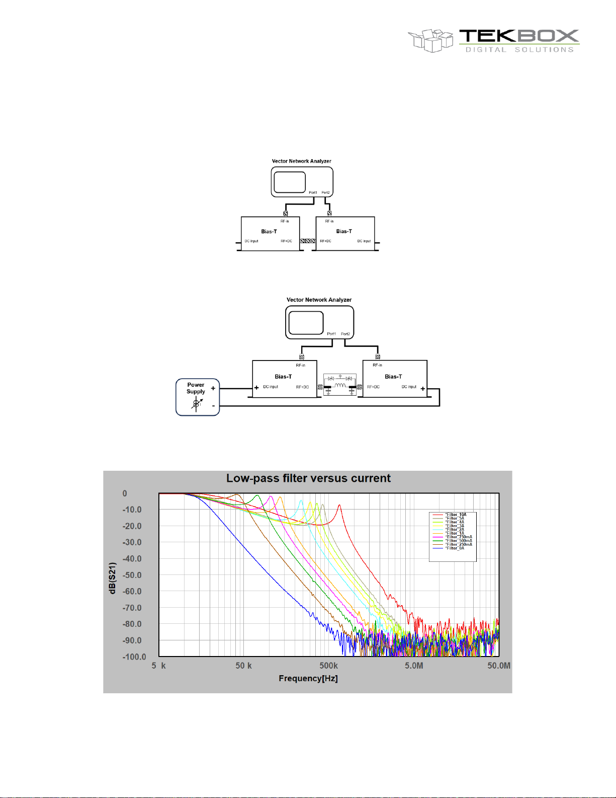
8.2 EMC-filter characteristics versus load current
1) Connect two Bias-Tees using coaxial adapters as depicted below and make a through calibration
2) Connect the test PCB with the EMC-filter in between two Bias-Tees and measure S21 for various bias
currents
Note that the EMC – Filter is measured in a 50 Ohm system. In real applications, the filter is terminated with the
source and load impedance.
EMC low-pass filter characteristics; 0 – 10A load current
Page 7
V1.0
TBBT01
Bias-Tee, 5 kHz – 1.2 GHz, 5 - 10A
7
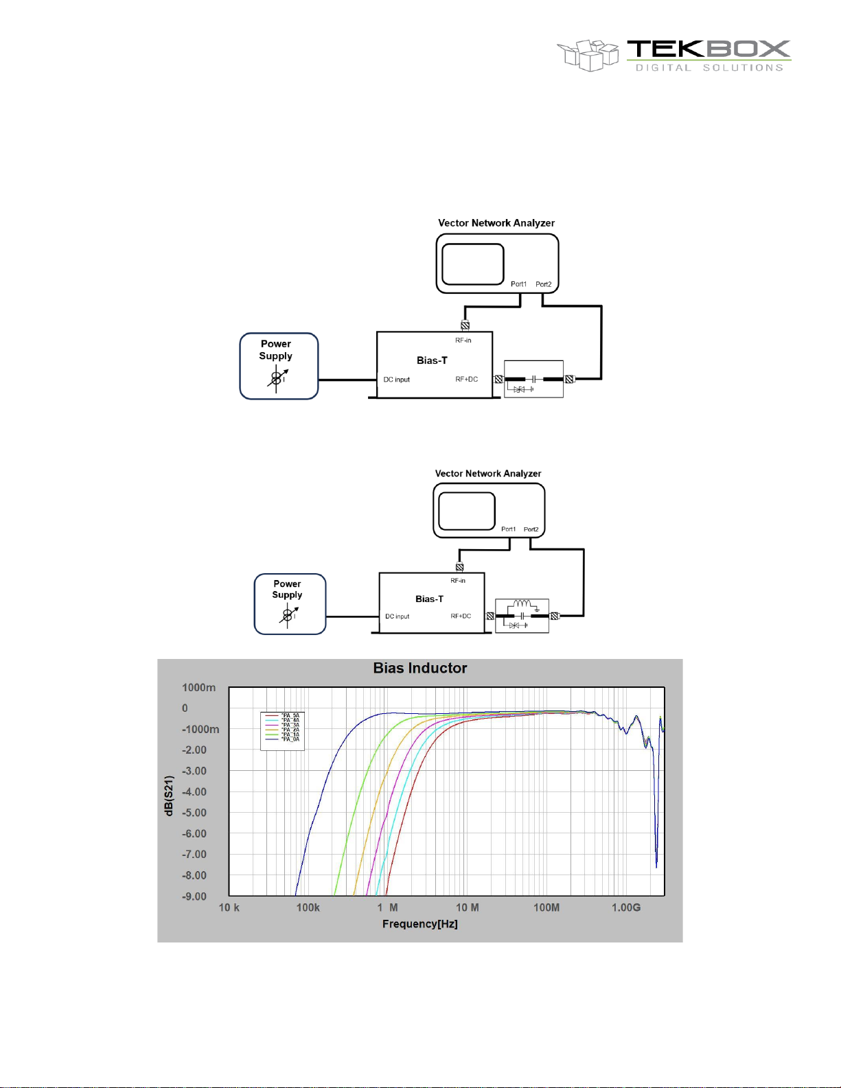
8.3 RF choke versus supply current
1) To investigate suitability of an RF choke for a RF power amplifier output transistor, make a through
calibration of a setup as depicted below.
2) Next add the RF choke and measure its effect on the S21 of the output path.
Insertion loss caused by an RF choke; 5 turns on a 43 material core 5943007601; 0 to 5A
Page 8
V1.0
TBBT01
Bias-Tee, 5 kHz – 1.2 GHz, 5 - 10A
8
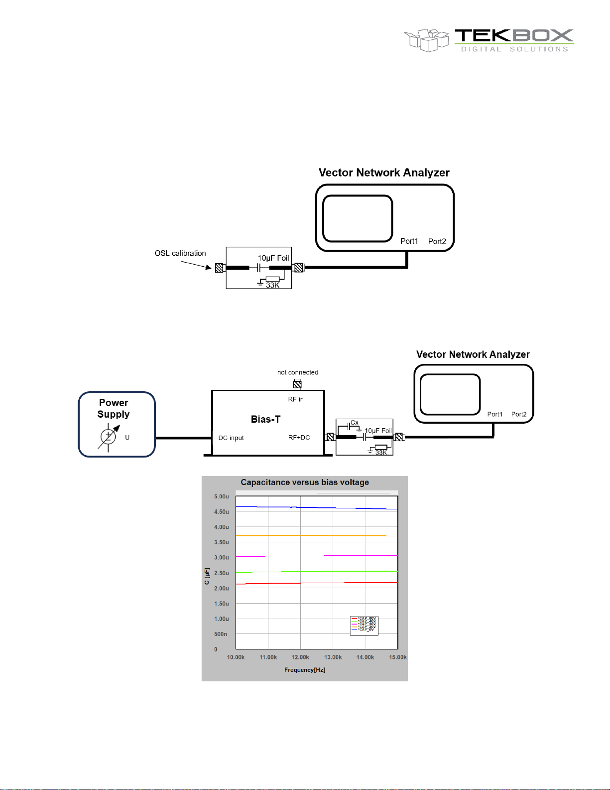
8.4 Capacitor versus bias voltage
1) To investigate capacitance versus bias voltage, prepare a test PCB as depicted below and perform a
single channel S11 OSL calibration at low frequency, e.g. from 10kHz – 15kHz. As decoupling capacitor,
use a large, high voltage foil capacitor; e.g. ≥ 10µF / 200V
2) Solder the capacitor under test to the test-PCB as depicted below and measure the capacitance
(imaginary part of S11) for various bias voltages
Capacitance variation versus bias voltage; 4.7µF/50V, X7R, 1206; CL31B475KBHVPNE
Page 9
V1.0
TBBT01
Bias-Tee, 5 kHz – 1.2 GHz, 5 - 10A
9
9 Optional Accessories - Test PCBs
TBBT01-TPCB1
Test PCB for inductor saturation measurement
TBBT01-TPCB2
Test PCB for EMC filter measurement
TBBT01-TPCB3
Test PCB for RF choke measurement
TBBT01-TPCB4
Test PCB for capacitor measurement
10 Ordering Information
Part Number
Description
TBBT01
Bias-Tee, 1 pc. female terminal block Phoenix Contact 1762592
Optional Accessories:
Part Number
Description
TBBT01-TPCB1
Test PCB for inductor saturation measurement
TBBT01-TPCB2
Test PCB for EMC filter measurement
TBBT01-TPCB3
Test PCB for RF choke measurement
TBBT01-TPCB4
Test PCB for capacitor measurement
TBBT01-Through_N/M
Coaxial through adapter, N-male
TBBT01-Through_N/F
Coaxial through adapter, N-female
11 History
Version
Date
Author
Changes
V1.0
14.7.2023
Mayerhofer
Creation of the document
TekBox Digital Solutions Vietnam Pte. Ltd. www.tekbox.com
Factory 4, F4, Lot I-3B-1, Saigon Hi-Tech Park, Tan Phu Ward, District 9, Ho Chi Minh City, Vietnam
 Loading...