

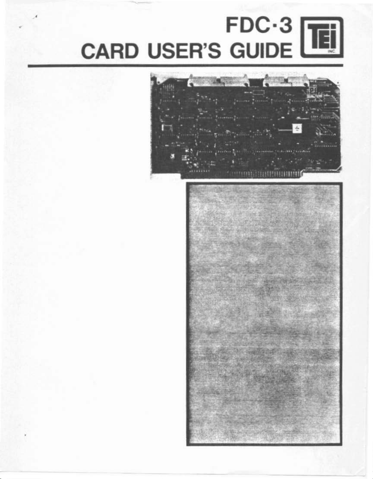
TEI FDC-3 User Manual
•
•
CARD USER'S GUIDE
FDC·3
li-
..
Et
FDC-3
FLOPPY-DISK
USER
CONTROLLER
MANUAL
I IKTRODUCTION
1.1
1.2
General
Physical
Description
CON
TEN
T
1-1
1-1
II
III
IV
V
VI
A
INSTALLATION
THEORY
3.1
3.2
3.3
3.4
3.5
3.6
3.7
3.8
SOFTWARE
4.1
4.2
HARDWARE
5.1
5.2
USER
TEl,
A.l
A.2
A.3
OF
OPERATION
Address
Drive-Select
Function-Select
Bidirectional
Read/Write
1791
Controller
Miscellaneous
Jumper
CONSIDERATIONS
FDC-3
1791
Device
CONSIDERATIO~S
Drive
Signal-Cable
REPAIR GUIDE
INC.
T/DOS DISKETTE READ/WRITE
General
Commands
Error-Recovery
Decoder
Latch
Bus
Clock
Logic
Selection
Card
Configuration
Connections
Logic
Buffers
Generation
of
Various
Procedures
Functions
ERROR
2-1
3-1
3-1
3-1
3-1
3-3
3-5
3-7
3-9
4-1
4-1
5-1
5-1
6-1
INDICATIONS
A-I
A-I
P.-4
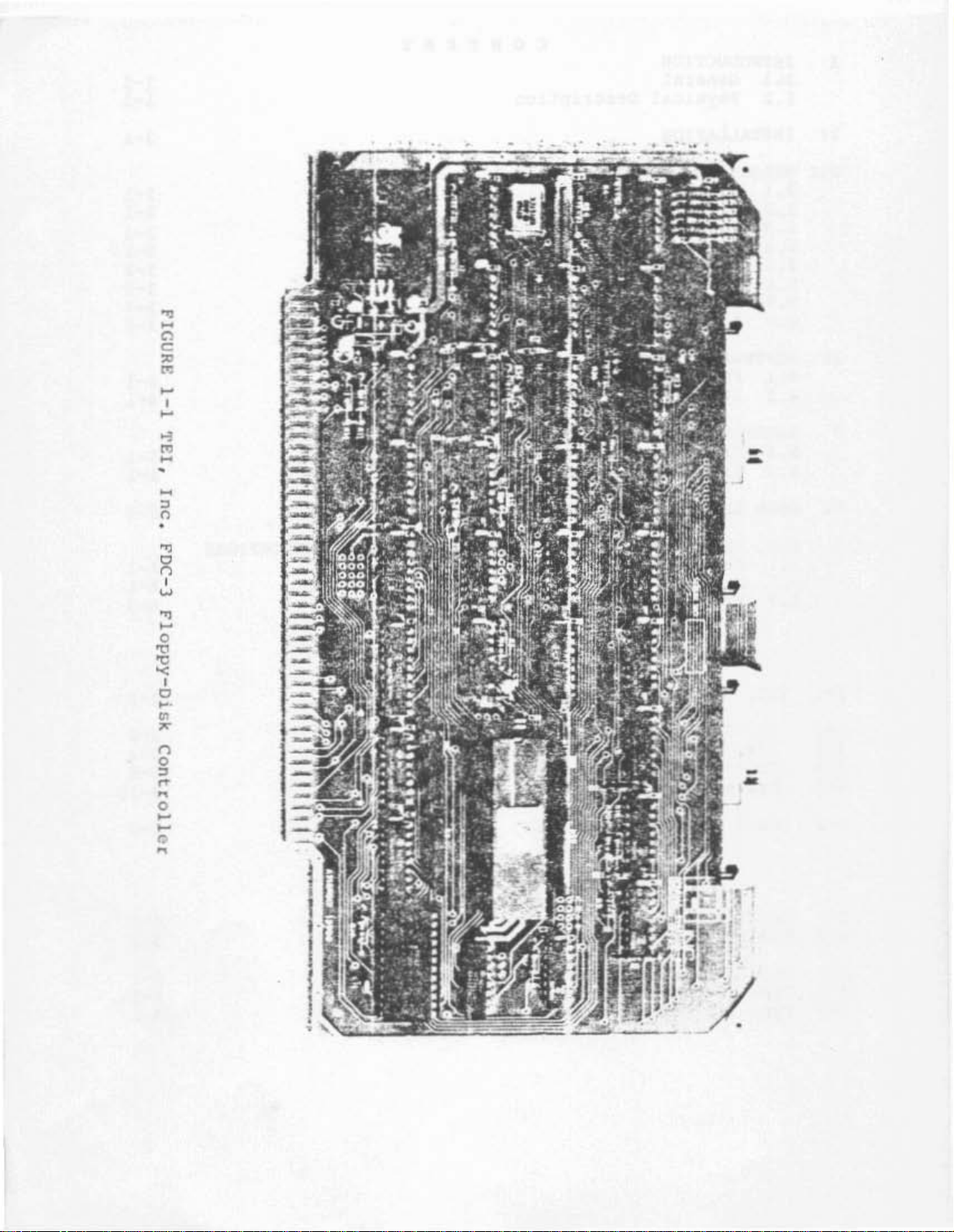
1-1
3-1
3-2
3-3
3-4
6-1
5-1
5-2
A-I
A-2
A-3
TEl,
Inc.
FDC-3
1791
Device
FDC-3
Drive-Ready
Card
Ejector,
Regular
Miniature
Type
Type
Type
I Command
II
III
FDC-3
Card
Card
Drive
Drive
Command
Command
Block
Block
Address
Delay
Left
Signal
Signal
Codes
Codes
FIG
Floppy-Disk
Diagram
Diagram
Jumper
Jumper
SidE
TAB
Connections
Connections
Codes
U
RES
Controller
Selection
Selection
L E S
1-0
3-0
3-4
3-8
3-10
6-0
5-2
5-3
A-I
A~2
A-2
i
..
"
g
•
..
,
-
-
•
..
-
-
•
•
..
-
~
,
c
••
•
..
o
g
..
•
o
-
Q
-
•
SECTION
INTRODUCTION
I
1.1
The
TEl,
GENERAL
floppy-disk
eight
sided,
standard
single
selection
system
The
conf
FDC-3
compatible
automatic
detection.
The
to
system
TEl,
operate
components.
Inc.
properly
manufacturer's
so.
1.2
The
FDC-3
PHYSICAL
circuits,
diskette-drive
drive
signal
fiberglass
S-IOO
long
bus
life.
Inc.
FDC-3
controller
drives
or
of
both
iguration.
Floppy-Disk
formats;
track-seek
FDC-3
reliably
in
another
components,
DESCRIPTION
Controller
plus
supporting
signal
cable;
double-sided
connector
Floppy-Disk
and
double
density
Controller
buffered
with
Floppy-Disk
in
a
Although
manufacturer's
card
cable;
all
etched-circuit
that
device
up
to
density.
and
verification;
TEl,
the
TEl,
(Figure
components;
and
mounted
has
gold-plated
Controller
and
supporting
three
The
number
also
control,
Controller
Inc.
ComFuter
FDC-3
Inc.
a
34-pin
on
mini
drives
1791
of
sides
effers
data,
was
Floppy-Disk
computer,
cannot
1-1)
guarantee
consists
50-pin
socket
a
5"
board
contacts
combines
logic
device
for
such
and
CRC
specifically
System
socket
for
x
10"
complete
the
to
control
-
single
allows
ease
features
and
status
generation
using
Controller
or
with
that
of
31
for
standard
miniature
(127-mm
with
for
reliability
1791
up
or
double-
software
in
changing
as
lines,
designed
TEl,
may work
another
it
will
integratec
(5.25")
x 254-mill)
a
standard
LSI
to
IBM-
and
Inc.
do
(8")
and
1-1
SECTION
II
INSTALLATIOK
1)
2)
3)
4)
5)
6)
Turn
System
CAUTION!
Install
card,
2
Note
in
Plug
that
backwards.
signal
drive(s)
(5.25")
connector
Turn
(or
System
lower)
doors
Place
for
memory-size
program,
Check
System
NEVER
card
install
plugs
drive(s)
(s)
open,
System
or
CRT
is
power
INSTALL
in
any
the
edge-connector
cable(s)
firmly
on,
with
information
FDC-3
diskette(l)
press
Display.
ready
for
off.
card
in
into
plugs
seated.
card
prompt,
RETURN
If
operation.
OR
same
into
large
all
will
T/DOS
REMOVE
slot.
slot
location
FDC-3
connector.
into
drive
appears
not
in
drive
then
to
load
Version
A CIRCUIT
If
the
FDC-3
to
avoid
card.
small
doors
open.
(after
work
properly.
A(2),
enter
maximum
CARD
having
prevents
Cable
Cable
connector.
CRT
close
size
size
2.0
(or
WITH
card
replaces
to
plugging
from
from
If
T/DOS
warmup)
drive
(in
K)
automatically.
higher)
POWER
move
the
standard
miniature
Be
Version
with
door,
for
installed,
ON!
an
FDC-
cables.
card
(8")
sure
1.44
drive
wait
desired
(1)
Consult
diskette
insertion
Write-Protected,
(2)TEI,
T/DOS
Press
and
8
Inc.
Version
key
to
load
8
local
Systems
2.0
to
load
from
documentation,
method
if
recording
with
(or
higher)
from
drive
drive
D.
on
eight
your
on
from
B,
Supervisor,
System.
disk
et
function
drives
key
or
Dealer
Diskette
te
requi
keys
7
to
B,
load
red.
on
C,
from
keyboard,
or
should
D,
drive
for
if
2-1
correct
not
can
desired.
C,
keys
be
load
7
Do
DI
A2-A7
AD.
SINP
SOUT
PD
BIN
PWR
Al
Drive-Select
Latch
Bidirectional
Buss
Driver
Address
Decoder
I .
MatrIx
Function
Select
Logic
Reset
~
/
......
A2
---
R/W
Dal
....
,-
....
,-
.....
".
.....
".
Dr
1791
ive
#
Datil
/
i'
v
i'
v
i'
'/
,
'/
I'
/
G
......
1/
......
1/
Clk
Rd
Clk
Earlv
Lat0
Write
Write
Di
rect
Step
Head
Head
Write
Write
Index
Ready
Track.
Data
Gate
ion
Load
Loadedl
Fault
Protect
Pulse
0
I
Read/Write
Clock
Generator
-
~
..
-
Delay
~
-----0
Delav
Raw
Dat
a
....
::.
DRIVE
~
"
....
1
F
"
......
"
I
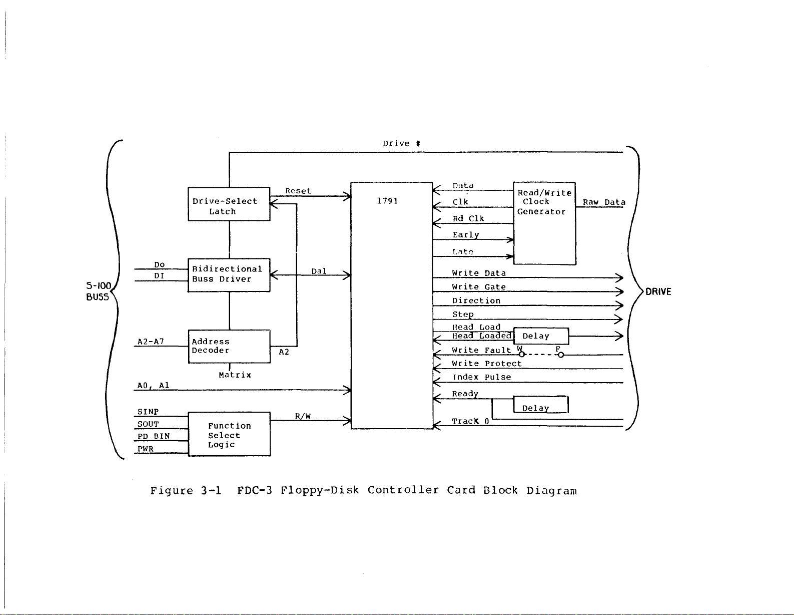
Figure
3-1
FDC-3
Floppy-Disk
Controller
Card
Block
Diagram
SECTION
III
The
an
TEl,
Address
Inc.
Decoder,
Bidirectional
Generator
controller,
3.1
The
basic
(high-order
selected
with
and
ADDRESS
FDC-3
address
on
software-controlled
card
Comparator
decoder.
edge
3.8)
When
Address
or
enables
•
the
1791
Z26
The
CPU
Decoder
FDC-3
Bus
Digital
miscellaneous
DECODER
address
the
FDC-3
device
and
three-row
the
jumper
sends
enables
THEORY
Floppy-Disk
Drive-Select
Buffers,
is
byte
not
card,
to
direct
register
gates
by
five-column
selection
date.
to
the
OF
OPERATION
Controller
crystal-controlled
phase-Locked
logic.
XXOY
to
XXFY
decoded
and
the
Y
accompa~ying
(Section
in
Z24
the
card
and
address
to
receive
Latch,
(hex)
on
FDC-3
is
partly
3.6).
Z25
matrix
described
Lelected
Card
(Figure
Function-Select
loop,
type
where
card),
jumpered
data
form
between
above
or
transmit
Read/Write
xx
0
to
byte
the
Z26
(and
by
the
3-1)
1791
is
"don't-care"
F
is
and
to
the
FDC-3
and
in
jumpers,
data.
contains
Latch,
Clock
MOS
jumper-
partly
proper
address
the
card
Section
LSI
the
3.2
Z30
and
drive
reset.
Data
on
enters
to
the
ignored.
3.3
Ga
tes
condition
3.4
Z28
BIDIRECTIONAL
and
DRIVE-SELECT
gates
in
numbers,
the
the
FDC-3
data
latch
address,
Z24
type
when
LATCH
and
(mini
bus
the
FUNCTION-SELECT LOGIC
inZ9,
Z29
Z24
onboard
are
and
logic
BUS
four-bic
Z25
BUFFERS
Z25
or
(low
order
operating
with
address
decode
to
receive
bidirectional
form
standard),
CPU
an
eight-bit
byte
system
bit
commands
or
transmit
bus
latch
side
with
number,
TEl,
executes
A2
high.
to
the
the
driver/receivers.
for
Inc.
an
OUT
Bits
FDC-3
proper
the
density,
CPU-85
instruction
Al
and
to
data.
selected
and
card)
AO
are
steer
or
3-1
3.5
READ/WRITE
CLOCK
GENERATION
The
Read/Write
Accurately
(single
clocks
This
logic
Write-Data
Digital
3.5.1
R24,
R25,
oscillator
3.5.2
Z12
divides
Z14
enables
drive
4,
8,
signals.
or
3.5.3
separating
density)
for
either
consists
Delay
Phase-Locked
OSCILLATOR
Xl,
and
output
DIVIDERS
the
cne
The
16
MHz--
WRITE-DA'I'A
Clock
or
MFH
recording
of
Generator,
Loop.
two
clocks
AND
16-MHz
of
the
selected
to
the
DELAY
Generator
incoming
mode
(double
mode.
a
crystal-controlled
multiplexer-controlled
sections
the
of
Divider
MULTIPLEXED
oscillator
four
buffers
buffer
Digital
GENERATOR
performs
data
and
density);
Z16
form
log~c.
BUFFER
signal
in
passe~
to
Z13,
the
Phase-Lc'cked
AND
BUFFER
the
clocks
and
Oscillator,
a
16-~Hz
generate
steered
selected
Loop.
dual
function
in
either
(2)
Supplying
oscillator.
Dividers,
Buffers,
2,
4
and
by
density
frequency
FM
of
mode
write
8
MHz.
(1)
and
The
ana
--2,
Z5
delays
as
required
buffers
3.5.4
Zl,
Z2,
circuit
electronics
pulses.
ZIA
and
clock.
transition.
Clock.
ZlB,
Z2B,
the
for
in
Z6,
DIGITAL
Z4,
ZlO,
receives
and
Z2A
synchronize
Z2B
and
and
Write
Data
write
steered
PHASE-LOCKED
211
and
combined
accurately
gates
These
pulses
buffers
signal
one,
precompensation.
by
Early
and
LOOP
Z16
data
form
and
separates
incoming
in
Z10
output
clock
in
Z16
and
Z17
three
Late
a
Digital
clock
signal
Zll
sel~ct
Z14
outputs
transitions
the
transitions
short
and
or
five
enables
from
Phase-Locked
clock
pulses
pulses
Z4
which
the
1791
16-MHz
one
the
from
with
for
output
device
clock
of
1791
from
each
the
loop.
the
the
the
the
clock.
times
four
device.
This
drive
data
FDC-3
input
Read
3-3
 Loading...