

Page 1

4040A
50 MHz PXI Differential
Instrumentation Amplifier
MODEL 4040A
NOTE: This User’s Manual was as current as possible when this product was manufactured. However, products
are constantly being updated and improved. To ensure you have the latest documentation, refer to
www.tegam.com.
10 TEGAM WAY • GENEVA, OHIO 44041 • 440-466-6100 • FAX 440-466-6110 • sales@tegam.com
Instruction Manual
PN# 4040A-840
Publication Date: June 2012
REV. E
Page 2

TABLE OF CONTENTS
TABLE OF CONTENTS
1 INSTRUMENT DESCRIPTION
Instrument Description .............................................................................1-1
Figure 1.1: Block Diagram of the 4040A .................................................1-1
Performance Specifications ........................................................................1-2
Functional Considerations ..........................................................................1-4
Frequency Response Curves ......................................................................1-5
2 PREPARATION FOR USE
Unpacking & Inspection.............................................................................2-1
Safety Information & Precautions ...............................................................2-1
Terms in this Manual ...........................................................................2-1
Terms as Marked on Equipment ............................................................2-1
Grounding the 4040A ...........................................................................2-2
Danger Arising from the Loss of Ground .................................................2-2
Do not Use in Explosive Environments ...................................................2-2
Power Source .....................................................................................2-3
3 OPERATING INSTRUCTIONS
PXI Installation ........................................................................................3-1
Front Panel Description .............................................................................3-2
4 SOFTWARE
5 SERVICE INFORMATION
Cleaning .................................................................................................5-1
Performance Verification Procedure ............................................................5-1
Computer Set-up ................................................................................5-2
CMMR ................................................................................................5-2
Offset Adjustment ...............................................................................5-4
DC Gain .............................................................................................5-6
AC Gain .............................................................................................5-7
Parts Replacement ...................................................................................5-12
Preparation for Calibration or Repair Service ................................................5-12
Expedite Repair and calibration Form ..........................................................5-13
Warranty .................................................................................................5-14
Warranty Limitations ...........................................................................5-14
Statement of Calibration ......................................................................5-14
10 TEGAM WAY • GENEVA, OHIO 44041 • 440-466-6100 • FAX 440-466-6110 • sales@tegam.com
I
Page 3
INSTRUMENT DESCRIPTION
SECTION 1
INSTRUMENT DESCRIPTION
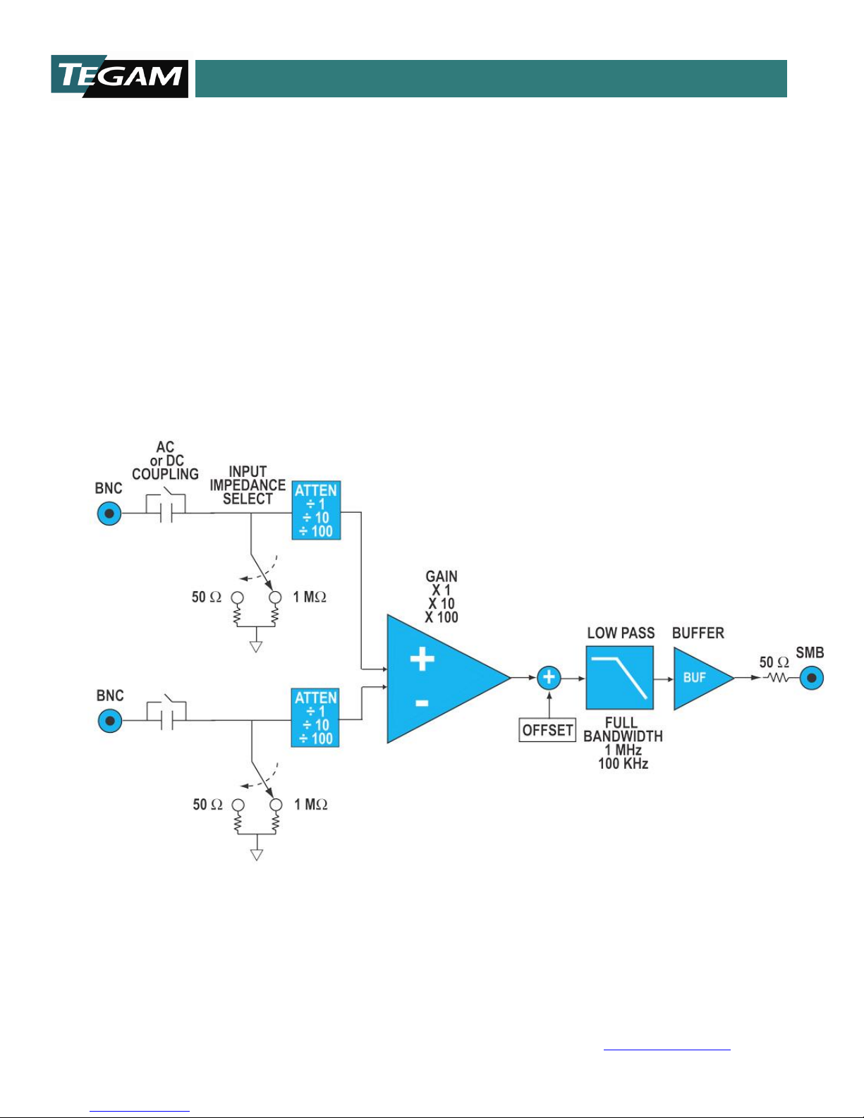
The 4040A is a single channel, differential input amplifier capable of high gain and equally high
attenuation values with a bandwidth from DC-50 MHz. The Model 4040A is capable of operating with
gains of x1, x10, and x100 in conjunction with attenuation by factors of: ÷1, ÷10, and ÷100. These
levels of gain and attenuation may be used in combination to condition a differential input signal so
that it matches the needed input of a low-level device such as a digitizer or oscilloscope. There is a
more in depth explanation contained in the specification section. In addition, the 4040A provides
programmable offset, anti-aliasing filters, input impedance and input coupling. Figure 1.1 is a block
diagram of the 4040A. The 4040A has been specifically designed to take two signals and make a valid
differential measurement by inverting one of the signals and adding the difference, this allows the user
to measure signals not referenced to local ground without compromising safety.
Figure 1.1: Block Diagram of the 4040A
10 TEGAM WAY • GENEVA, OHIO 44041 • 440-466-6100 • FAX 440-466-6110 • sales@tegam.com
1-1
Page 4
INSTRUMENT DESCRIPTION
Net Gain
Input
Attenuation
Internal
Amplifier
Gain
Peak AC Input
Amplitudes
(V) d per
channel
a,b,c,d
Max
Differential
Voltage (V)
w/o clipping
a,b,c,d
Max
Volts to
Chassis
a,b,c
Noise,
Referred to
Input
-3 dB
Bandwidth
÷100
÷100
X1
< 100
< 100
100 V
990 nV/√Hz
20 MHz
÷10
÷10
X1
< 10
< 10
40 V
99 nV/√Hz
20 MHz
÷10
÷100
X10
< 10
< 10
100 V
990 nV/√Hz
50 MHz 1 ÷1
X1
< 1
< 1
4 V
9 nV/√Hz
20 MHz
1
÷10
X10
< 1
< 1
40 V
99 nV/√Hz
50 MHz
1
÷100
X100
< 1
< 1
100 V
990 nV/√Hz
20 MHz
10
÷1
X10
< 0.1
< 0.1
4 V
9 nV/√Hz
50 MHz
10
÷10
X100
< 0.1
< 0.1
40 V
99 nV/√Hz
20 MHz
100
÷1
X100
< 0.01
< 0.01
4 V
9 nV/√Hz
20 MHz
a. DC Coupled, 1 MΩ input
b. AC Coupled, 1 MΩ input: DC + Peak AC not to exceed 100 V; Peak AC component not to exceed table
c. 5 Vrms max into 50 Ω
d. DAC offset adjustment to zero
PERFORMANCE SPECIFICATIONS
The multiple gain and attenuation settings of the 4040A interact to affect the performance in terms of
bandwidth and noise. Table 1.1 shows the various combinations and how these settings modify what
can be expected from the 4040A.
Table 1.1: Various Combination Possibilities of the 4040A
As an example, a total system gain of X1 can be achieved three different ways depending on the signal
requirements through attenuating and amplifying by different amounts. Choosing the best combination
involves trade offs in input amplitude, bandwidth and signal to noise ratio. Noise increases with higher
levels of attenuation because the noise specification is referred to the input. In relative terms the
signal to noise ratio is basically constant.
10 TEGAM WAY • GENEVA, OHIO 44041 • 440-466-6100 • FAX 440-466-6110 • sales@tegam.com
1-2
Page 5

INSTRUMENT DESCRIPTION
Input Specifications Value Clarification
Channels Single Channel Differential Input
Gains 100, 10, 1, 0.1, 0.01
Maximum Voltage Range ±100 V DC + Peak AC
Coupling AC, DC In AC 10 Hz and above
Input Impedance 1 MΩ | | 20 pF, 50 Ω ±1%, Selectable
Input Voltage Range ±100 V For Gain 0.01 @ 1 MΩ Input Impedance
±10 V For Gain 0.1 @ 1 MΩ Input Impedance
±5 V For Gain 0.1 @ 50 Ω Input Impedance
±1 V For Gain 1
±0.1 V For Gain 10
±0.01 V For Gain 100
Connection Type BNC Jacks 50 Ω, Quantity 2
Common Mode Rejection Ratio
(CMRR) 77 dB at 60 Hz For Gain setting of x1, x10 and x100 & Attenuation
(> 50 dB at 1 MHz) setting of ÷1
57 dB at 60 Hz For Attenuation setting of ÷10
37 dB at 60 Hz For Attenuation setting of ÷100
Total Harmonic Distortion <-60 db @ 1 MHz Output 1 Vp-p into 50 Ω
DC Gain Accuracy ± (0.1% |input| + 100 µV) Offset set to 0 for Gain 10, 1, 0.1, 0.01
± (1.5% |input| + 300 µV) Offset set to 0 for Gain 100
(Basic) AC Gain Accuracy ±0.15 dB Attenuation of 1, Gain of 1,
See Figures 1.2, 1.3 and 1.4 for other settings
Over-voltage Protection ±100 V DC + Peak AC
(In Any Range)
Offset Range 0 to ± Full Scale Full Scale output of ±1 V into 50 Ω,
All Gain Ranges
Offset Resolution 38 µV per step 65,535 total DAC steps into 50 Ω
Offset Accuracy ±(0.5% of |Setting| + 300 µV) Referenced to 1 V Range
Temperature Stability ±(0.01% of |rdg| + 40 µV)/°C All Gain Ranges
Noise 9 nV/√Hz CMR=±1 V, Gain 10 and 100
Referred to Input for Frequencies >100 Hz
Rise Time ≤3.5 ns
Output Specifications Value Clarifications
Maximum Output Voltage ±1 V Single Ended into 50 Ω
Connection Type SMB Jack 50 Ω
Output Impedance 50 Ω ±1%
LP Filter, Cutoff Frequency 100 kHz, 1 MHz Single Pole Filter
Bandwidth See Table 1.1
Passband Flatness See Figures 1.2, 1.3 and 1.4 Limits off charts will not exceed ±3 dB for the
for limits Bandwidths listed in Table 1.1
Environmental
Specifications Value
Operating Temperature 0 °C to +45 °C, (32 °F to 113 °F) Ambient
Storage Temperature -20 °C to +50 °C (-4 °F to +122 °F)
Humidity Range <80% RH Non-Condensing
Warm-up Time 30 minutes
10 TEGAM WAY • GENEVA, OHIO 44041 • 440-466-6100 • FAX 440-466-6110 • sales@tegam.com
1-3
Page 6

INSTRUMENT DESCRIPTION
Functional Considerations
Voltage & Current Limitations
In general, the maximum input voltage of the 4040A should not exceed ±100 V (200 Vp-p) when the
input terminator is set to 1 MΩ. However, some settings will produce incorrect results at lower
voltages. This occurs when the input signal or gain setting is too high and causes the output amplifier
to clip the signal. An example of this would be measuring a 10 V signal with the gain set to x100.
Mathematically this results in a 1000 V signal which clearly exceeds the 2 Vp-p rating of the output
amplifier. See Table 1.1 for a table of appropriate input voltages for given combinations of gain and
attenuation. No damage would occur to the 4040A or to a digitizer connected to it if the input range
was exceeded, but the signal would be distorted. A signal in excess of 100 V would cause the onboard
voltage limiting circuitry to activate and also create distortion.
There are other considerations when the 4040A is configured with the 50 Ohm input termination. The
input voltage is limited to a maximum of ±5 Vrms. This is due to the power limitations of the
terminator which is 2 W. To preserve the signal integrity and bandwidth of the amplifier the 50 Ohm
terminator is protected with surface mount single use fuses.
Important: Exceeding the rating of the input in this case requires the 4040A to be returned to the
factory for service.
Frequency Characteristics
The 4040A is capable of amplifying mill-volt level signals with a bandwidth from DC to 50 MHz. Some
combinations of gain and attenuation will limit the bandwidth to 20 MHz. See Table 1.1 for a complete
list of settings and the expected bandwidth. In addition, AC coupling rolls off the low frequencies at 10
Hz.
Two anti-aliasing low pass filters are included and tuned for 100 KHz and 1 MHz. These are first order
filters that roll off at 20 dB per decade.
Offset Adjustment
The 4040A includes a programmable offset adjustment that operates on the signal after the gain
stage. The resolution of the adjustment is 38 µV and can offset the signal ±1 V which is the entire
range of the output amplifier. It is not able to effectively offset a signal that exceeds the input range of
a given gain and attenuation setting.
Selecting Gains and Ranges
The amplitude of the signal being measured is the primary consideration when selecting the
appropriate gain and attenuation settings. As an example: A 100 mV signal that is riding on 42 V can
be effectively measured with an attenuation setting of ÷100 and a gain setting of x10. This is because
the differential operation of the 4040A rejects the 42 V common mode signal and only amplifies the
difference producing an output signal of 1 V. If the signal of interest was the 42 V itself the 4040A
should be configured with an attenuation of ÷100 and a gain of x1 producing an output signal of 0.42
V. The 4040A attenuates the signal prior to amplification.
10 TEGAM WAY • GENEVA, OHIO 44041 • 440-466-6100 • FAX 440-466-6110 • sales@tegam.com
1-4
Page 7
INSTRUMENT DESCRIPTION
Gain Deviation from Nominal (No Attenuation)
(Typical Data and Test Limits)
-0.5
-0.4
-0.3
-0.2
-0.1
0
0.1
0.2
0.3
0.4
0.5
1.0E+03 1.0E+04 1.0E+05 1.0E+06 1.0E+07 1.0E+08
Frequency (Hz)
Gain Error (dB)
1/1 Li mit
10/1 Li mi t
100/1 Li mi t
1/1 POS
1/1 NEG
10/1 POS
10/1 NEG
100/1 POS
100/1 NEG
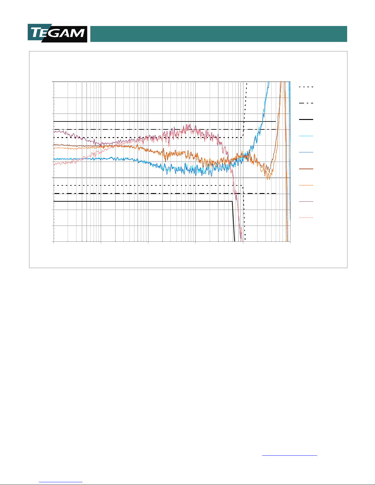
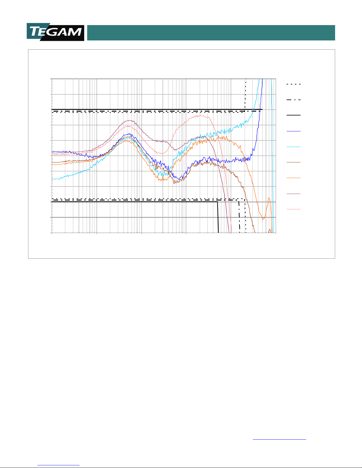
Figure 1.2: Frequency Response Curves
Figure 1.2 depicts the typical frequency response curves from the nominal gain values with no
attenuation applied by the 4040A. The three different black bands, above and below the curves, give
the allowable limits for passband flatness for the different gain/attenuation settings. Individual plots
are given for both the positive and negative inputs of the 4040A for all gain/attenuation settings. For
example, to find the expected passband flatness from 10 kHz to 10 MHz to achieve an inverted gain of
100, the 100/1 NEG plot would be used in conjunction with the solid black limit lines. These lines are
used because the first number is for the gain, and the second number is for attenuation, POS for
positive, and NEG for negative. The expected passband flatness would be ±0.25 dB from 10 kHz to 6
MHz and +0.25 dB to -3 dB from 6 MHz to 10 MHz.
10 TEGAM WAY • GENEVA, OHIO 44041 • 440-466-6100 • FAX 440-466-6110 • sales@tegam.com
1-5
Page 8
INSTRUMENT DESCRIPTION
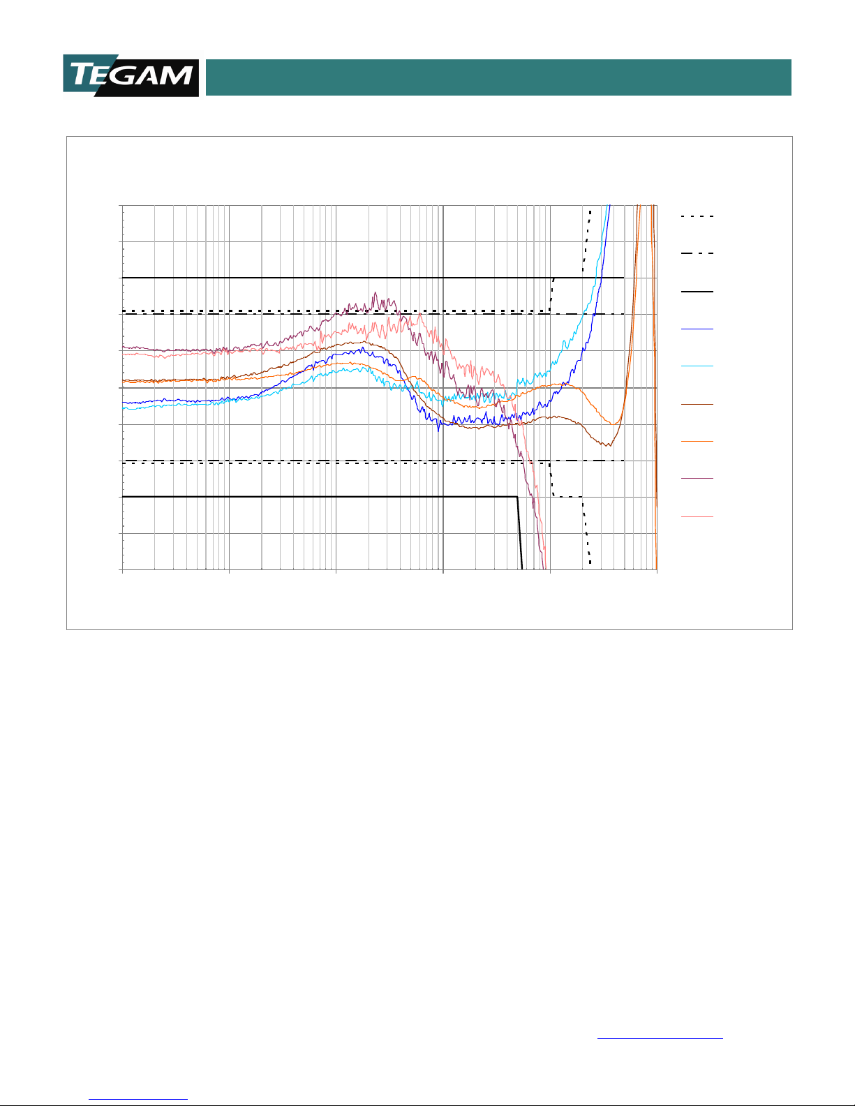
Gain Deviation from Nominal ÷10 Attenuation
(Typical Data and Test Limits)
-0.5
-0.4
-0.3
-0.2
-0.1
0
0.1
0.2
0.3
0.4
0.5
1.0E+03 1.0E+04 1.0E+05 1.0E+06 1.0E+07 1.0E+08
Frequency (Hz)
Gain Error (dB)
1/10 Li mi t
10/10 Li mi t
100/10 Limi t
1/10 POS
1/10 NEG
10/10 POS
10/10 NEG
100/10 POS
100/10 NEG
Figure 1.3 depicts the typical frequency response curves from the nominal gain values with an
attenuation of 10 applied by the 4040A. As with Figure 1.2, the three different black bands, above and
below the curves, give the allowable limits for passband flatness for the different gain/attenuation
settings. Individual plots are given for both the positive and negative inputs of the 4040A for all
gain/attenuation settings. For example, to find the expected passband flatness from 1 kHz to 7 MHz to
achieve an inverted gain of 10, the 100/10 NEG plot would be used in conjunction with the solid black
limit lines. These lines are used because the first number is for the gain, and the second number is for
attenuation, POS for positive, and NEG for negative. The expected passband flatness would be ±0.3 dB
from 1 kHz to 5 MHz and +0.3 dB to -3 dB from 5 MHz to 7 MHz.
Figure 1.3: Frequency Response Curves
10 TEGAM WAY • GENEVA, OHIO 44041 • 440-466-6100 • FAX 440-466-6110 • sales@tegam.com
1-6
Page 9
INSTRUMENT DESCRIPTION
Gain Deviation from Nominal ÷100 Attenuation
(Typical Data and Test Limits)
-0.5
-0.4
-0.3
-0.2
-0.1
0
0.1
0.2
0.3
0.4
0.5
1.0E+03 1.0E+04 1.0E+05 1.0E+06 1.0E+07 1.0E+08
Frequency (Hz)
Gain Error (dB)
1/100 Li mi t
10/100 Limi t
100/100 Limi t
1/100 POS
1/100 NEG
10/100 POS
10/100 NEG
100/100 POS
100/100 NEG
Figure 1.4: Frequency Response Curves
Figure 1.4 depicts the typical frequency response curves from the nominal gain values with an
attenuation of 100 applied by the 4040A. As with Figure 1.2 & 1.3, the three different black bands,
above and below the curves, give the allowable limits for passband flatness for the different
gain/attenuation settings. Individual plots are given for both the positive and negative inputs of the
4040A for all gain/attenuation settings. For example, to find the expected passband flatness from 100
kHz to 25 MHz to achieve a gain of 1, the 100/100 POS plot would be used in conjunction with the
solid black limit lines. These lines are used because the first number is for the gain, and the second
number is for attenuation, POS for positive, and NEG for negative. The expected passband flatness
would be ±0.3 dB from 100 kHz to 5 MHz and +0.3 dB to -3 dB from 5 MHz to 20 MHz. 20 MHz is the
bandwidth limit for the 4040A in this setting. If 25 MHz is needed a setting of 10/10 or 1/1 can be
used as long as the input voltages for those ranges are not exceeded.
10 TEGAM WAY • GENEVA, OHIO 44041 • 440-466-6100 • FAX 440-466-6110 • sales@tegam.com
1-7
Page 10

PREPARATION FOR USE
!
!
This symbol denotes where precautionary information may be found.
!
Attention – Please refer to the instruction manual.
SECTION 2
PREPARATION FOR USE
UNPACKING & INSPECTION
Each TEGAM Model 4040A is put through a series of electrical and mechanical inspections before
shipment to the customer. Upon receipt of your instrument unpack all of the items from the shipping
carton and inspect for any damage that may have occurred during transit. Report any damaged items
to the shipping agent. Retain and use the original packing material for reshipment if necessary.
Upon Receipt, inspect the carton for the following items:
(1) Model 4040A Fast PXI Instrumentation Amplifier
(1) CD including Model 4040 User’s Manual, P/N 4040-901-01A and Software Drivers, P/N 1000019
SAFETY INFORMATION & PRECAUTIONS
The following safety information applies to both operation and service personnel. Safety precautions
and warnings may be found throughout this instruction manual and the equipment. These warnings
may be in the form of a symbol or a written statement. Below is a summary of these precautions.
Terms in This Manual:
“CAUTION” A statement to identify conditions or practices that could result in damage to the
equipment, or other property.
“WARNING” A statement to identify conditions or practices that could result in personal injury or loss
of life.
Terms as Marked on Equipment:
“CAUTION” Indicates a personal injury hazard not immediately accessible as one reads the marking, or
a hazard to property including the equipment itself.
“DANGER” Indicates a personal injury hazard immediately accessible as one reads the marking.
10 TEGAM WAY • GENEVA, OHIO 44041 • 440-466-6100 • FAX 440-466-6110 • sales@tegam.com
2-1
Page 11

PREPARATION FOR USE
!
!
!
!
Precaution
Grounding the Model 4040A
The Model 4040A is grounded through the grounding conductor of the PXI chassis power cord. The
connection shields of all the connectors are also grounded. The proper grounding of the chassis is
essential for safety and for the optimization of the Model 4040A’s operation.
WARNING
To avoid electrical shock or other potential safety hazards, plug the PXI chassis power cord into a
properly wired receptacle before using this instrument.
Use A Common Ground for All Instruments
It is very important that all instruments being used, both internal modules as well as external
instruments share a common ground. If a common ground connection is lost then improper
instrumentation readings may result, also see warning above.
Danger Arising from Loss of Ground
If the connection to ground through the PXI chassis is lost or compromised, a floating potential could
develop in the Model 4040A module. Under these conditions all accessible parts, including insulating
parts such as the front panel could develop a hazardous voltage and put the user at risk.
Do Not Use in Explosive Environments
WARNING: The Model 4040A is not designed for operation in explosive environments.
Do not Operate Unless the 4040A Module is Properly Installed
WARNING: The Model 4040A should be properly seated within an appropriate PXI chassis before use.
All PXI chassis covers and service panels should be in place before operation. Operation with empty
module slots, or removed covers could result in personal injury.
PXI Chassis:
WARNING: The power supply should be plugged in (to establish ground) but switched off before
installing the Model 4040A or any PXI module.
10 TEGAM WAY • GENEVA, OHIO 44041 • 440-466-6100 • FAX 440-466-6110 • sales@tegam.com
2-2
Page 12

PREPARATION FOR USE
!
!
Use Care When Servicing with Power On
Dangerous voltages may exist at several points within the PXI chassis. To avoid personal injury or
damage, avoid touching exposed connections or components while the power is on. Assure that the
power is off and any cables are disconnected when removing or servicing the 4040A amplifier.
Power Source
The Model 4040A is designed to connect to a PXI Chassis and receive all operational power from the
backplane of the chassis. The Model 4040A draws 3.3 volts and 5 volts from the PXI Chassis
backplane. 3.3 DC volts are used for all TTL level functions and 5 VDC operate onboard analog
circuitry. Be aware that higher voltages exist within the PXI Chassis and it is essential that the chassis
is powered off and all cables disconnected when installing or uninstalling any PXI card. A protective
chassis ground connection by way of the grounding conductor in the power cord is essential for safe
operation.
WARNING:
DO NOT MODIFIY any configurations or connections from their original state otherwise safe operation
of this equipment may be compromised.
WARNING:
Always remember to shut off the power and wait at least 15 seconds before disconnecting or
connecting any cables to or from the Model 4040A. Ignoring this warning could result in electric shock.
10 TEGAM WAY • GENEVA, OHIO 44041 • 440-466-6100 • FAX 440-466-6110 • sales@tegam.com
2-3
Page 13

OPERATING INSTRUCTIONS
PXI Empty Slot and Module Guides
CPCI / PXI Connector
Injector / Ejector Handle
Differential Inputs
Output (2 Vp-p Max)
SECTION 3
OPERATING INSTRUCTIONS
PXI Installation
Follow the steps below to install the Model 4040A Fast PXI Instrumentation Amplifier.
1. Make sure the power is off or turn off the power of the PXI chassis.
2. Read the manual supplied with the PXI chassis to determine which slot is available for standard
PXI modules such as the Model 4040A. Slot 1 is usually reserved for use as a hardware controller
for the overall system, or other modular device to enable PXI control.
3. Install the 4040A by inserting the module into a PXI chassis empty slot by placing the card edges
into the front module guides, guides are located on both the top and bottom of the chassis entry
location.
4. Gently apply pressure to further insert the card and finally use the injector/ejector handle on the
4040A to fully insert the card into the chassis.
5. Secure the 4040A to the chassis with the captured screw in the top of the face plate.
Figure 3.1: Installation of the 4040A into a typical multi-slot PXI chassis
10 TEGAM WAY • GENEVA, OHIO 44041 • 440-466-6100 • FAX 440-466-6110 • sales@tegam.com
3-1
Page 14

OPERATING INSTRUCTIONS
Connections
Both of the amplifier’s inputs require standard BNC 50 Ω connections and have an impedance of 1 MΩ
or 50 Ω. The 4040A is compatible with all signals from DC to 50 MHz and 0 to ±100 V. The output is
an SMB jack connector specified as 50 Ω with an output impedance of 50 Ω. For proper performance,
TEGAM recommends interconnection cables made of RG316-DS. RG316-DS accessory cables are
available from TEGAM in various lengths to suit your application or you may purchase them from
standard cable vendors.
Both input BNC shields are grounded to a common ground inside the Model 4040A. The BNC shield is
at the same potential as the PXI chassis ground. Figure 3.2 represents a typical connection from the
4040A to a system under test.
Figure 3.2: Typical Connection
10 TEGAM WAY • GENEVA, OHIO 44041 • 440-466-6100 • FAX 440-466-6110 • sales@tegam.com
3-2
Page 15

SOFTWARE
SECTION 4
SOFTWARE
VISA compliant drivers are available for LabVIEW 8, C++ and Visual Basic. Installation instructions are
contained in the Readme.txt in 4040A DRIVER zip file on the CD that is included with the 4040A. It can
also be downloaded from the website, www.tegam.com.
The 4040A driver installer does not allow customization of the installation path. The setup will create a
Tegam4040 folder in C:\Program Files\National Instruments\LabVIEW 8.2\instr.lib folder. The whole
tegam4040 folder can be copied to the instr.lib folder for later LabVIEW versions. A simple front panel
LabVIEW VI, Tegam4040 - Control [Demo].vi is included in C:\Program Files\National
Instruments\LabVIEW 8.2\instr.lib\Tegam4040\Examples folder that provides control of all of the
4040A’s settings.
10 TEGAM WAY • GENEVA, OHIO 44041 • 440-466-6100 • FAX 440-466-6110 • sales@tegam.com
4-1
Page 16

SERVICE INFORMATION
SECTION 5
SERVICE INFORMATION
CLEANING
AVOID THE USE OF CHEMICAL CLEANING AGENTS WHICH MIGHT
DAMAGE THE UNIT. DO NOT APPLY ANY SOLVENT CONTAINING
KETONES, ESTERS OR HALOGENATED HYDROCARBONS.
Use low-velocity compressed air to blow off the accumulated dust. Hardened dirt can be removed with
a cotton-tipped swab, soft, dry cloth.
VERIFICATION PROCEDURE
Equipment Required:
Network Analyzer: Agilent 4395A or equivalent
5 ½ digit Digital Multimeter (DMM) (Qty 2): Fluke 8840A or equivalent
DC voltage source capable of 10 mV - 10 V with the capability of a switched output, BNC output
PXI Chassis: NI PXI-1033 or equivalent
Computer with required software installed; LabVIEW
Tegam 4040-Control [Demo].vi LabVIEW Application (Provided with the unit)
N-type male to N-type male adapters
N-type male to N-type male patch cable
N-type male to BNC female adapters (Qty 5)
BNC Male to BNC Male Adapter
BNC Female to BNC Female Adapter
BNC to BNC cables 3’ (Qty 3)
50 Ω ± 0.1 Ω BNC feed thru terminators (Qty 2), one to be marked with a red dot.
SMB Female to BNC Female adapter
SMB Male to BNC Female adapters (Qty 2)
Dual Banana jack to BNC Male connector
Dual Banana plug to BNC Female connectors (Qty 2)
N-Type Power-Splitter 50 Ω
Two way splitters (Qty 2)
1000 µF Non-Polarized Filter Cap (Qty 2)
Identical BNC to BNC cables as short as possible (Qty 2)
Special Instructions: UUT designates Unit Under Test.
10 TEGAM WAY • GENEVA, OHIO 44041 • 440-466-6100 • FAX 440-466-6110 • sales@tegam.com
5-1
Page 17

SERVICE INFORMATION
3
2
Computer Set-Up
LabVIEW 4040A Front Panel Control
1. Double click on “Tegam4040A - Control [Demo].vi”.
2. From the Visa Tegam4040 I/O drop down box, select the appropriate slot of the
4040A card.
3. Press the Run Arrow button on the toolbar.
Figure 5.1: Tegam4040A - Control [Demo].vi Front Panel
A. Common Mode Rejection Ratio, Gain of 1
Note: CMRR = (differential gain dB) – (common mode gain dB), the 4395A Network Analyzer will
be displaying the common mode gain dB. The differential gain dB is equal to the gain setting of
the 4040A, example: 4040A set for 20 dB gain (gain of 10), common mode gain must be less
than -60 dB for a CMRR of less than 80 dB.
10 TEGAM WAY • GENEVA, OHIO 44041 • 440-466-6100 • FAX 440-466-6110 • sales@tegam.com
5-2
Page 18

SERVICE INFORMATION
1 3 2
4 5 6
7
8
Figure 5.2: Connections for CMMR
1. Connect the N-type power splitter’s input to the 4395A Network Analyzer’s RF Out,
using an N-type male to male adapter.
2. Connect one end of the N-type power splitter’s output to the 4395A Network
Analyzer’s R, using an N-type patch cable.
3. Connect an N-Type to BNC Female adapter to the remaining end of the N-Type Power-
Splitter.
4. Connect the two identical short BNC to BNC cables to the “+” and “-“ inputs of the
UUT.
5. Connect the BNC “T” to both the identical BNC cables.
6. Connect a 50 Ω load to the BNC “T”.
7. Connect a BNC to BNC cable from the N-type power splitter to the 50 Ω load.
8. Connect a BNC to BNC cable to the A input of the 4395A Network Analyzer.
9. Connect a SMB male to BNC female adapter to the previously connected BNC cable
and the output of the UUT.
10. Change the setting in the Tegam4040A - Control [Demo].vi application as follows:
a) Attenuation of 1
10 TEGAM WAY • GENEVA, OHIO 44041 • 440-466-6100 • FAX 440-466-6110 • sales@tegam.com
5-3
Page 19

SERVICE INFORMATION
11. Change the setting on the 4395A Network Analyzer as follows:
a) Network Analyzer Mode
b) Bandwidth for 10 Hz
c) Start frequency to 50 Hz
d) Stop frequency to 70 Hz
e) Scale Reference to 20 dB/div
f) Source Power to +15 dB
g) Statistics On
12. Measure the common mode gain @ 60 Hz. Tolerance <-80 dB.
13. Change the setting in the Tegam4040A - Control [Demo].vi application as follows:
a) Gain of 10
14. Measure the common mode gain @ 60Hz. Tolerance <-60 dB.
15. Change the setting in the Tegam4040A - Control [Demo].vi application as follows:
a) Gain of 100
16. Measure the common mode gain @ 60 Hz. Tolerance <-40 dB.
17. Disconnect the setup from the UUT.
B. Offset Adjustment of UUT
Note: Do not perform this portion of the procedure until called out by any other section of this
procedure.
1. If no connections are made to the UUT’s output, then:
a) Connect the Dual Banana plug to BNC female adapter into the DMM 1 Input.
Observe Polarity.
b) Connect a 1000 µF Non-Polarized Filter Cap into the side of the previous step’s
connector.
c) Connect a BNC to BNC cable to the dual banana plug in step a.
d) Connect a SMB male to BNC female adapter to the other end of the BNC cable
connected in the previous step.
e) Connect the SMB adapter connected to the DMM 1, to the OUT of the UUT.
2. Verify the DMM 1 is set for DC voltage and Auto Range.
3. Change the “DAC” setting up or down of the “Tegam4040A - Control [Demo].vi”
program until the displayed reading of the 8840A is zero. The reading on the display of
the 8840A must be less than ±0.08 mV for all gains except 40 dB. The reading must
be less than ±0.30 mV for the 40 dB gain setting. One count (hex) is ≈ 76.3 µV
4. Disconnect the 8840A Set-up from the UUT.
1. Meas, Analyzer Type, Network Analyzer
1. Bw/Avg, 1, 0, X1
1. Start, 5, 0, X1
1. Stop, 7, 0, X1
1. Scale Ref, 2, 0, X1
1. Source, 1, 5, X1
1. Utility, Statistics on/off
10 TEGAM WAY • GENEVA, OHIO 44041 • 440-466-6100 • FAX 440-466-6110 • sales@tegam.com
5-4
Page 20

SERVICE INFORMATION
3 4 5
5a 6 8 9 9a
10
C. DC Gain Checks -40 dB, -20 dB & 0 dB
Figure 5.3: Connections for DC Gain
1. Turn off the output of the DC voltage source.
2. Change the setting on the DC voltage source to output 5.00 VDC.
3. Connect a two way BNC connector to the “+” input of the UUT.
4. Connect the Red 50 Ω terminator to one side of the connector in the previous step.
5. Connect a Dual Banana plug to BNC female adapter into the DMM 2 Input. Observe
Polarity.
a) Connect a 1000 µF Non-Polarized Filter Cap into the side of the previous step’s
connector.
6. Connect a BNC to BNC cable in between the DMM 2 and the unused end of the two
way BNC connector on the UUT “+” input.
7. Connect a 50 Ω terminator to the “-“ input of the UUT.
8. Connect a BNC to BNC cable in between the DC voltage source and the Red 50 Ω
terminator.
9. Connect a Dual Banana plug to BNC female adapter into the DMM 1 Input. Observe
Polarity.
a) Connect a 1000 µF Non-Polarized Filter Cap into the side of the previous step’s
connector.
10. Connect a BNC to BNC cable to the adapter connected in the previous step.
11. Connect a SMB male to BNC female adapter to the end of the BNC connected in the
previous step.
12. Connect the cable and SMB adapter to the output of the UUT.
13. Change the setting in the Tegam4040A - Control [Demo].vi application as follows:
a) Attenuation of 100
b) Gain of 1
Note: Do not disconnect any connections from the UUT for the next Step.
Note: Do not touch or move any wires after performing the next step.
10 TEGAM WAY • GENEVA, OHIO 44041 • 440-466-6100 • FAX 440-466-6110 • sales@tegam.com
5-5
Page 21

SERVICE INFORMATION
14. Perform the Offset Adjustment of UUT section at this time skipping any steps that
say to connect or disconnect anything.
15. Press the Offset button on the DMM 2.
16. Turn on the output of the DC voltage source.
17. Measure both the DMMs displayed readings. The DMM 1 is the Voltage Out, and the
DMM 2 is the Voltage In. Calculate the percentage difference by (dividing the voltage
out by 2, divided by the gain setting (0.01,0.1,1,10,100), minus the voltage input),
divided by the voltage input. Tolerance ±0.1%
18. Turn off the output of the DC voltage source.
19. Press the Offset button on the DMM 2.
20. Change the setting in the Tegam4040A - Control [Demo].vi application as follows:
a) Attenuation of 10
21. Repeat steps 14—19.
22. Swap the two connections to the inputs of the UUT. The cables and splitter shall
remain connected to the Red 50 Ω terminator.
23. Repeat steps 13—21.
24. Set the DC voltage source to output 1.00 VDC.
25. Change the setting in the Tegam4040A - Control [Demo].vi application as follows:
a) Attenuation of 1
26. Repeat steps 14—19.
27. Swap the two connections to the inputs of the UUT. The cables and splitter shall
remain connected to the Red 50 Ω terminator.
28. Repeat steps 14—19.
D. DC Gain check 20 dB
1. Set the DC voltage source to output 0.100 VDC.
2. Change the setting in the Tegam4040A - Control [Demo].vi application as follows:
a) Gain of 10
Note: Do not disconnect any connections from the UUT for the next Step.
Note: Do not touch or move any wires after performing the next step.
3. Perform the Offset Adjustment of UUT section at this time skipping any steps that
say to connect or disconnect anything.
4. Press the Offset button on the DMM 2.
5. Turn on the output of the DC voltage source.
6. Measure both the DMMs displayed readings. The DMM 1 is the Voltage Out, and the
DMM 2 is the Voltage In. Calculate the percentage difference by (dividing the voltage
out by 2, divided by the gain setting (0.01,0.1,1,10,100), minus the voltage input),
divided by the voltage input. Tolerance ± 0.1%
7. Turn off the output of the DC voltage source.
8. Press the Offset button on the DMM 2.
9. Swap the two connections to the inputs of the UUT. The cables and splitter shall
remain connected to the Red 50 Ω terminator.
10. Repeat steps 3—8.
E. DC Gain Adjustment 40 dB
1. Set the DC voltage source to output 0.010 VDC.
10 TEGAM WAY • GENEVA, OHIO 44041 • 440-466-6100 • FAX 440-466-6110 • sales@tegam.com
5-6
Page 22

SERVICE INFORMATION
1
2 3 6
8
5
2. Change the setting in the Tegam4040A - Control [Demo].vi application as follows:
a) Gain of 100
Note: Do not disconnect any connections from the UUT for the next Step.
Note: Do not touch or move any wires after performing the next step.
3. Perform the Offset Adjustment of UUT section at this time skipping any steps that
say to connect or disconnect anything.
4. Press the Offset button on the DMM 2.
5. Turn on the output of the DC voltage source.
6. Measure both the DMMs displayed readings. The DMM 1 is the Voltage Out, and the
DMM 2 is the Voltage In. Calculate the percentage difference by (dividing the voltage
out by 2, divided by the gain setting (0.01,0.1,1,10,100), minus the voltage input),
divided by the voltage input. Tolerance ±1.5%
7. Turn off the output of the DC voltage source.
8. Press the Offset button on the DMM 2.
9. Swap the two connections to the inputs of the UUT. The cables and splitter shall
remain connected to the Red 50 Ω terminator.
10. Repeat steps 3—8.
11. Disconnect setup from UUT.
F. Verification of 20 dB & 40 dB Attenuation
10 TEGAM WAY • GENEVA, OHIO 44041 • 440-466-6100 • FAX 440-466-6110 • sales@tegam.com
Figure 5.4: Connections for AC Gain
5-7
Page 23

SERVICE INFORMATION
14
15
1. Connect the N-type power splitter’s input to the 4395A Network Analyzer’s RF Out,
using an N-type male to male adapter.
2. Connect one end of the N-type power splitter’s output to the 4395A Network
Analyzer’s R, using an N-type patch cable.
3. Connect an N-Type to BNC Female adapter to the remaining end of the N-Type Power-
Splitter.
4. Connect two 50 Ω terminators to both inputs of the UUT, the one with Red, on top.
5. Connect a BNC to BNC cable to remaining N-type power splitter.
6. Connect a BNC to BNC cable to the A input of the 4395A Network Analyzer.
7. Connect a SMB male to BNC female adapter to the previously connected BNC cable.
8. Connect the two BNC to BNC cables from the 4395A together using a SMB female to
BNC female adapter.
9. Change the setting in the Tegam4040A - Control [Demo].vi application as follows:
a) Attenuation of 10
b) Gain of 1
10. Repeat the Offset Adjustment of UUT section.
11. Change the setting on the 4395A Network Analyzer as follows:
a) Bandwidth for 100 Hz
1. Bw/Avg, 1, 0, 0, X1
b) Start frequency to 1 kHz
10 TEGAM WAY • GENEVA, OHIO 44041 • 440-466-6100 • FAX 440-466-6110 • sales@tegam.com
Figure 5.5: Connections for AC Gain
5-8
Page 24

SERVICE INFORMATION
c) Stop frequency to 50 MHz
d) Sweep Type to Log Frequency
e) Scale Reference to 0.25 dB/div with a Reference Value of -20 dB
f) Calibrate the system
g) Stop frequency to 10 MHz
12. Disconnect the two SMB adapters from each other.
13. Remove the SMB female to BNC adapter from the BNC cable connected to the power
splitter.
14. Connect the BNC Cable from power splitter to the 50 Ω load of the “+” input of the
UUT.
15. Connect the SMB male adapter end, connected to the A of the 4395A, to the OUT of
the UUT.
16. Verify the final values for the frequency response curve to not exceed -20 dB ±0.2 dB
for the -20 dB and -40 dB ±0.3 dB for the -40 dB settings.
17. Change the setting on the 4395A Network Analyzer as follows:
a) Stop frequency to 50 MHz
18. After the cursor has swept the entire frequency, verify the frequency response curve to
not exceed -20 or -40 dB ±3 dB.
19. Change the setting on the 4395A Network Analyzer as follows:
a) Stop frequency to 10MHz
20. Swap the two loads connected to the inputs of the UUT. The cable shall remain
connected to the Red 50 Ω terminator.
21. Repeat steps 16—19.
22. Change the setting in the Tegam4040A - Control [Demo].vi application as follows:
a) Attenuation of 100
23. Change the setting on the 4395A Network Analyzer as follows:
a) Scale Reference Value of -40 dB
24. Repeat steps 16—19.
25. Swap the two loads connected to the inputs of the UUT. The cable shall remain
connected to the Red 50 Ω terminator.
26. Repeat steps 16—19.
27. Disconnect the cables from the UUT, leaving the loads connected.
G. 0 dB Gain Check
1. Change the setting in the Tegam4040A - Control [Demo].vi application as follows:
a) Attenuation of 1
2. Repeat the Offset Adjustment of UUT section.
3. Connect the two BNC to BNC cables from the 4395A together using a SMB female to
BNC female adapter.
1. Start, 1, k/m
1. Stop, 5, 0, M/µ
1. Sweep, Sweep Type Menu, Log Freq
1. Scale Ref, ., 2, 5, X1, Reference Value, -, 2, 0, X1
1. Cal, Calibration Menu, Response, Thru
2. After the Cursor has swept across the frequency span, “Press ‘Done’ if
finished with Cal” is displayed, press the Done Response button.
1. Stop, 1, 0, M/µ
1. Stop, 5, 0, M/µ
1. Stop, 1, 0, M/µ
1. Scale Ref, Reference Value, -, 4, 0, X1
10 TEGAM WAY • GENEVA, OHIO 44041 • 440-466-6100 • FAX 440-466-6110 • sales@tegam.com
5-9
Page 25

SERVICE INFORMATION
4. Change the setting on the 4395A Network Analyzer as follows:
a) Scale Reference Value of 0 dB
b) Source Power to -4 dB
c) Calibrate the system
5. Disconnect the two SMB adapters from each other.
6. Remove the SMB female to BNC adapter from the BNC cable connected to the power
splitter.
7. Connect the BNC Cable from the power splitter to the Red 50 Ω load connected to the
“+” input of the UUT.
8. Connect the SMB male adapter, connected to the A of the 4395A, end to the OUT of
the UUT.
9. After the cursor has swept the entire frequency, verify the frequency response curve to
not exceed 0 dB ±3 dB.
10. Change the setting on the 4395A Network Analyzer as follows:
a) Stop frequency to 10 MHz
11. Verify the final values for the frequency response curve to not exceed 0 dB ±0.15 dB.
12. Swap the two loads connected to the inputs of the UUT. The cable shall remain
connected to the Red 50 Ω terminator.
13. Verify the final values for the frequency response curve to not exceed 0 dB ±0.15 dB.
14. Change the setting on the 4395A Network Analyzer as follows:
a) Stop frequency to 50 MHz
15. After the cursor has swept the entire frequency, verify the frequency response curve to
not exceed 0 dB ±3 dB.
16. Disconnect the cables from the UUT, leaving the loads connected.
H. 20 dB Gain Check
1. Change the setting in the Tegam4040A - Control [Demo].vi application as follows:
a) Gain of 10
2. Repeat the Offset Adjustment of UUT section.
3. Connect the BNC Cable from the power splitter to the Red 50 Ω load connected to the
“-” input of the UUT.
4. Connect the SMB male adapter, connected to the A of the 4395A, end to the OUT of
the UUT.
5. Change the setting on the 4395A Network Analyzer as follows:
a) Scale Reference Value of 20 dB
6. Verify the final values for the frequency response curve to not exceed 20 dB ±0.2 dB.
7. Swap the two loads connected to the inputs of the UUT. The cable shall remain
connected to the Red 50 Ω terminator.
8. Verify the final values for the frequency response curve to not exceed 20 dB ±0.2 dB.
9. Disconnect the cables from the UUT, leaving the loads connected.
1. Scale Ref, Reference Value, 0, X1
1. Source, -, 4, X1
1. Cal, Calibration Menu, Response, Thru
2. After the Cursor has swept across the frequency span, “Press ‘Done’ if
finished with Cal” is displayed, press the Done Response button.
1. Stop, 1, 0, M/µ
1. Stop, 5, 0, M/µ
1. Scale Ref, Reference Value, 2, 0, X1
10 TEGAM WAY • GENEVA, OHIO 44041 • 440-466-6100 • FAX 440-466-6110 • sales@tegam.com
5-10
Page 26

SERVICE INFORMATION
I. 40 dB Gain Check
1. Change the setting in the Tegam4040A - Control [Demo].vi application as follows:
a) Gain of 100
2. Repeat the Offset Adjustment of UUT section.
3. Connect the two BNC to BNC cables from the 4395A together using a SMB female to
BNC female adapter.
4. Change the setting on the 4395A Network Analyzer as follows:
a) If the memory card with saved settings is available:
b) Scale Reference Value of 40 dB
c) Stop frequency to 20 MHz
d) Source Power to -24 dB
e) Calibrate the system
5. Disconnect the two SMB adapters from each other.
6. Remove the SMB female to BNC adapter from the BNC cable connected to Bbox1.
7. Connect the BNC Cable from the power splitter to the Red 50 Ω load connected to the
“+” input of the UUT.
8. Connect the SMB male adapter, connected to the A of the 4395A, end to the OUT of
the UUT.
9. After the cursor has swept the entire frequency, verify the frequency response curve to
not exceed 40 dB +0.25 dB, -3 dB.
10. Change the setting on the 4395A Network Analyzer as follows:
a) Stop frequency to 6 MHz
11. Verify the final values for the frequency response curve to not exceed 40 dB ±0.25 dB.
12. Swap the two loads connected to the inputs of the UUT. The cable shall remain
connected to the Red 50 Ω terminator.
13. Verify the final values for the frequency response curve to not exceed 40 dB ±0.25 dB.
14. Change the setting on the 4395A Network Analyzer as follows:
a) Stop frequency to 20 MHz
15. After the cursor has swept the entire frequency, verify the frequency response curve to
not exceed 40 dB +0.25 dB, -3 dB.
16. Disconnect the setup.
J. UUT Disconnect
1. Press the Stop button on the “Tegam4040A - Control [Demo].vi” program.
2. Remove any cables that may be still connected to the UUT.
1. Press, RECALL, 4.STA, Skip steps b—d.
1. Scale Ref, Reference Value, 4, 0, X1
1. Stop, 2, 0, M/µ
1. Source, -, 2, 4, X1
1. Cal, Calibration Menu, Response, Thru
2. After the Cursor has swept across the frequency span, “Press ‘Done’ if
finished with Cal” is displayed, press the Done Response button.
1. Stop, 6, M/µ
1. Stop, 2, 0, M/µ
10 TEGAM WAY • GENEVA, OHIO 44041 • 440-466-6100 • FAX 440-466-6110 • sales@tegam.com
5-11
Page 27

SERVICE INFORMATION
Parts Replacement
The Model 4040A has no user-serviceable parts. All onboard parts besides the connectors are surface
mount based (SMT). The 4040A contains multiple levels of failsafe circuitry. As a last resort, four SMT
fuses have been installed which may blow if the 4040A is used outside of its rated operating
constraints. Since all onboard fuses are SMT devices, it is not suggested that they be replaced by the
user. If you suspect that the unit has failed, please contact TEGAM Inc. for an RMA number.
Preparation for Calibration or Repair Service
Once you have verified that a malfunctioning 4040A cannot be solved in the field and the need for
repair and calibration service arises, contact TEGAM customer service to obtain an RMA, (Returned
Material Authorization), number. You can contact TEGAM customer service via the TEGAM website,
www.tegam.com or by calling 440.466.6100 (All Locations) OR 800.666.1010 (United States Only).
The RMA number is unique to your instrument and will help us identify your instrument and to address
the particular service request by you which is assigned to that RMA number. Of even greater
importance is a detailed written description of the problem that should be attached to the instrument.
Many times repair turnaround is unnecessarily delayed due to a lack of repair instructions or of a
detailed description of the problem.
This description should include information such as is the problem intermittent?, when is the problem
most frequent?, has anything changed since the last time the instrument was used?, Etc. Any detailed
information provided to our technicians will assist them in identifying and correcting the problem in the
quickest possible manner. Use the form provided on the next page.
Once this information is prepared, sent it with the instrument and RMA number to our service
department, we will do our part in making sure that you receive the best possible customer service
and turnaround time possible.
10 TEGAM WAY • GENEVA, OHIO 44041 • 440-466-6100 • FAX 440-466-6110 • sales@tegam.com
5-12
Page 28

SERVICE INFORMATION
RMA#:
Instrument Model #:
Serial
Number:
Company:
Technical
Contact:
Phone
Number:
Additional
Contact Info:
Expedite Repair & Calibration Form
Use this form to provide additional repair information and service instructions. The Completion of this
form and including it with your instrument will expedite the processing and repair process.
Repair Instructions
Evaluation Calibration Only Repair Only Repair & Calibration Z540 (Extra Charge)
Detailed Symptoms
Include information such as measurement range, instrument settings, type of components being
tested, is the problem intermittent? When is the problem most frequent?, Has anything changed with
the application since the last time the instrument was used?, etc.
10 TEGAM WAY • GENEVA, OHIO 44041 • 440-466-6100 • FAX 440-466-6110 • sales@tegam.com
5-13
Page 29

SERVICE INFORMATION
Warranty
TEGAM, Inc. warrants this product to be free from defects in material and workmanship for a period of
one year from the date of shipment. During this warranty period, if a product proves to be defective,
TEGAM Inc., at its option, will either repair the defective product without charge for parts and labor, or
exchange any product that proves to be defective.
TEGAM, Inc. warrants the calibration of this product for a period of 6 months from date of shipment.
During this period, TEGAM, Inc. will recalibrate any product, which does not conform to the published
accuracy specifications.
In order to exercise this warranty, TEGAM, Inc., must be notified of the defective product before the
expiration of the warranty period. The customer shall be responsible for packaging and shipping the
product to the designated TEGAM service center with shipping charges prepaid. TEGAM Inc. shall pay
for the return of the product to the customer if the shipment is to a location within the country in
which the TEGAM service center is located. The customer shall be responsible for paying all shipping,
duties, taxes, and additional costs if the product is transported to any other locations. Repaired
products are warranted for the remaining balance of the original warranty, or 90 days, whichever
period is longer.
Warranty Limitations
The TEGAM, Inc. warranty does not apply to defects resulting from unauthorized modification or
misuse of the product or any part. This warranty does not apply to fuses, batteries, or damage to the
instrument caused by battery leakage.
The foregoing warranty of TEGAM is in lieu of all other warranties, expressed or implied. TEGAM
specifically disclaims any implied warranties of merchantability or fitness for a particular purpose. In no
event will TEGAM be liable for special or consequential damages. Purchaser’s sole and exclusive remedy
in the event any item fails to comply with the foregoing express warranty of TEGAM shall be to return
the item to TEGAM; shipping charges prepaid and at the option of TEGAM obtain a replacement item or
a refund of the purchase price.
Statement of Calibration
This instrument has been inspected and tested in accordance with specifications published by TEGAM
Inc. The accuracy and calibration of this instrument are traceable to the National Institute of Standards
and Technology through equipment, which is calibrated at planned intervals by comparison to certified
standards maintained in the laboratories of TEGAM Inc.
Contact Information:
TEGAM INC.
10, TEGAM WAY
GENEVA, OHIO 44041
PH: 440.466.6100
FX: 440.466.6110
CAGE Code: 49374
WEB: http://www.tegam.com
10 TEGAM WAY • GENEVA, OHIO 44041 • 440-466-6100 • FAX 440-466-6110 • sales@tegam.com
5-14
 Loading...