

Page 1
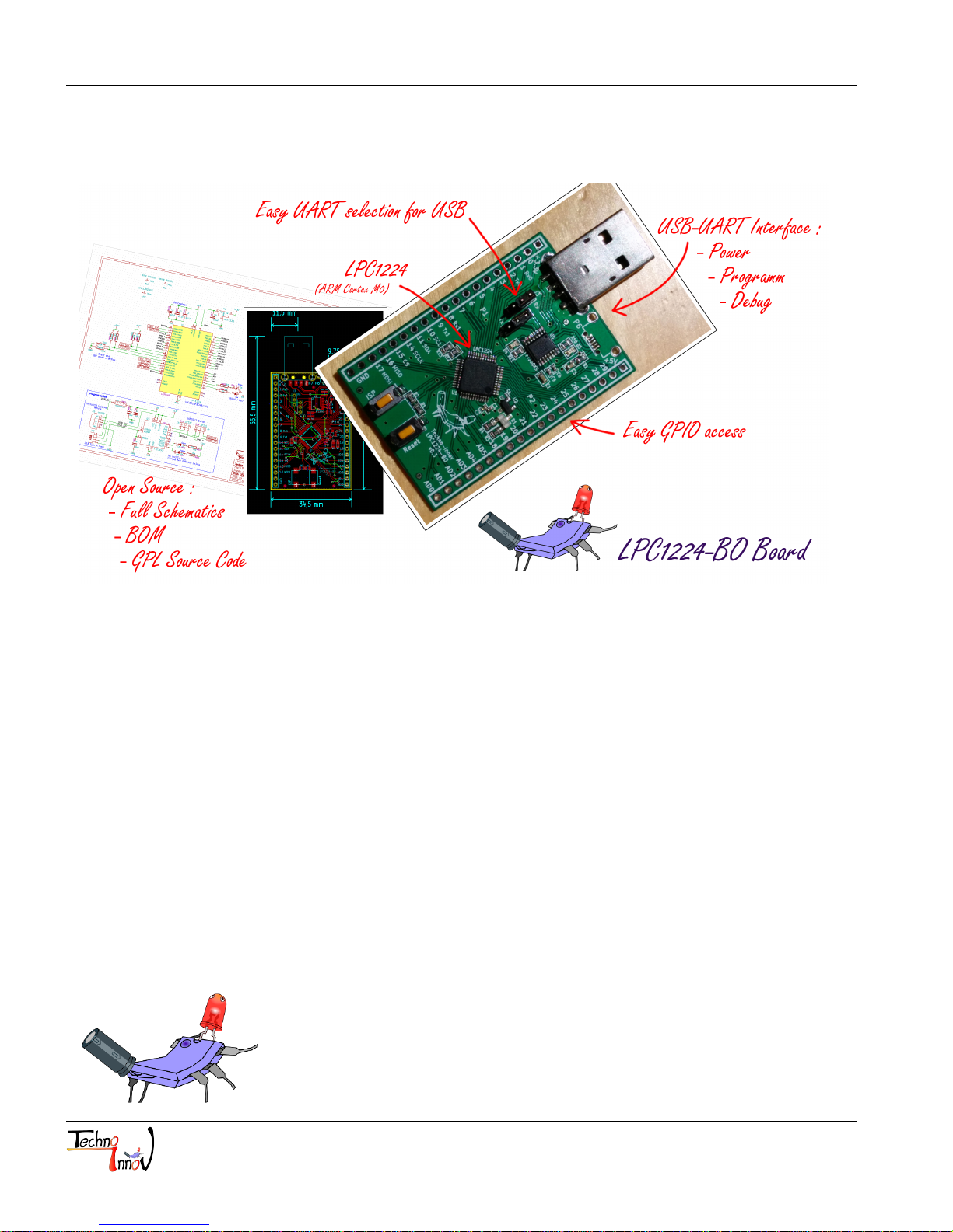
LPC1224_BO_SRM Board v0.3
LPC1224 break-out board
System
Reference Manual
LPC1224_BO_SRM for Board v0.3
September 10, 2015 - Doc rev 0.3b
Author: Nathaël Pajani
Techno-Innov - DomoTab
http://www.techno-innov.fr
page 1 / 22
Page 2
LPC1224_BO_SRM Board v0.3
Table des matières
1 Introduction 4
2 Licenses 4
2.1 Documentation . . . . . . . . . . . . . . . . . . . . . . . . . . . . . . . . . . . . . . . . . . . . . . . . 4
2.2 Hardware . . . . . . . . . . . . . . . . . . . . . . . . . . . . . . . . . . . . . . . . . . . . . . . . . . . 4
2.3 Software . . . . . . . . . . . . . . . . . . . . . . . . . . . . . . . . . . . . . . . . . . . . . . . . . . . . 4
3 Hardware 5
3.1 Dimensions . . . . . . . . . . . . . . . . . . . . . . . . . . . . . . . . . . . . . . . . . . . . . . . . . . 5
3.2 Connectors . . . . . . . . . . . . . . . . . . . . . . . . . . . . . . . . . . . . . . . . . . . . . . . . . . 5
3.2.1 P1 Connector . . . . . . . . . . . . . . . . . . . . . . . . . . . . . . . . . . . . . . . . . . . . . 6
3.2.2 P2 Connector . . . . . . . . . . . . . . . . . . . . . . . . . . . . . . . . . . . . . . . . . . . . . 7
3.2.3 P6 and P7 Connectors . . . . . . . . . . . . . . . . . . . . . . . . . . . . . . . . . . . . . . . . 7
3.3 Jumpers . . . . . . . . . . . . . . . . . . . . . . . . . . . . . . . . . . . . . . . . . . . . . . . . . . . . 8
3.3.1 J3 and J4 jumpers . . . . . . . . . . . . . . . . . . . . . . . . . . . . . . . . . . . . . . . . . . 8
4 Electronics 9
4.1 Micro-controller LPC1224 . . . . . . . . . . . . . . . . . . . . . . . . . . . . . . . . . . . . . . . . . . 9
4.1.1 Internal RAM . . . . . . . . . . . . . . . . . . . . . . . . . . . . . . . . . . . . . . . . . . . . . 10
4.1.2 Internal Flash . . . . . . . . . . . . . . . . . . . . . . . . . . . . . . . . . . . . . . . . . . . . . 10
4.1.3 Communication interfaces . . . . . . . . . . . . . . . . . . . . . . . . . . . . . . . . . . . . . . 10
4.1.4 GPIO . . . . . . . . . . . . . . . . . . . . . . . . . . . . . . . . . . . . . . . . . . . . . . . . . 10
4.1.5 ADC . . . . . . . . . . . . . . . . . . . . . . . . . . . . . . . . . . . . . . . . . . . . . . . . . . 10
4.1.6 Reset and ISP mode . . . . . . . . . . . . . . . . . . . . . . . . . . . . . . . . . . . . . . . . . 11
4.2 I2C . . . . . . . . . . . . . . . . . . . . . . . . . . . . . . . . . . . . . . . . . . . . . . . . . . . . . . . 11
4.3 User Led and Button . . . . . . . . . . . . . . . . . . . . . . . . . . . . . . . . . . . . . . . . . . . . . 11
4.4 USB to UART bridge . . . . . . . . . . . . . . . . . . . . . . . . . . . . . . . . . . . . . . . . . . . . 12
5 Software 13
5.1 Sample Source Code . . . . . . . . . . . . . . . . . . . . . . . . . . . . . . . . . . . . . . . . . . . . . 13
5.1.1 Grab the sources . . . . . . . . . . . . . . . . . . . . . . . . . . . . . . . . . . . . . . . . . . . 13
5.1.2 Sample code content . . . . . . . . . . . . . . . . . . . . . . . . . . . . . . . . . . . . . . . . . 13
5.1.3 Sample code entry point . . . . . . . . . . . . . . . . . . . . . . . . . . . . . . . . . . . . . . . 14
5.2 Building the binary . . . . . . . . . . . . . . . . . . . . . . . . . . . . . . . . . . . . . . . . . . . . . . 14
5.2.1 Get a toolchain . . . . . . . . . . . . . . . . . . . . . . . . . . . . . . . . . . . . . . . . . . . . 14
5.2.2 Build command and options . . . . . . . . . . . . . . . . . . . . . . . . . . . . . . . . . . . . . 15
5.2.3 Build process . . . . . . . . . . . . . . . . . . . . . . . . . . . . . . . . . . . . . . . . . . . . . 15
5.3 Uploading binary on target . . . . . . . . . . . . . . . . . . . . . . . . . . . . . . . . . . . . . . . . . 15
5.3.1 Tools . . . . . . . . . . . . . . . . . . . . . . . . . . . . . . . . . . . . . . . . . . . . . . . . . 15
5.3.2 Connection with target and upload . . . . . . . . . . . . . . . . . . . . . . . . . . . . . . . . . 15
6 Board revisions history 16
6.1 v01 . . . . . . . . . . . . . . . . . . . . . . . . . . . . . . . . . . . . . . . . . . . . . . . . . . . . . . . 16
6.2 v02 . . . . . . . . . . . . . . . . . . . . . . . . . . . . . . . . . . . . . . . . . . . . . . . . . . . . . . . 16
6.3 v03 . . . . . . . . . . . . . . . . . . . . . . . . . . . . . . . . . . . . . . . . . . . . . . . . . . . . . . . 16
7 Annexes 17
Techno-Innov - DomoTab
http://www.techno-innov.fr
page 2 / 22
Page 3
LPC1224_BO_SRM Board v0.3
7.1 Schematics . . . . . . . . . . . . . . . . . . . . . . . . . . . . . . . . . . . . . . . . . . . . . . . . . . 17
7.2 BOM . . . . . . . . . . . . . . . . . . . . . . . . . . . . . . . . . . . . . . . . . . . . . . . . . . . . . . 21
7.2.1 Block version . . . . . . . . . . . . . . . . . . . . . . . . . . . . . . . . . . . . . . . . . . . . . 21
7.2.2 Easy order version . . . . . . . . . . . . . . . . . . . . . . . . . . . . . . . . . . . . . . . . . . 22
7.3 Document revision History . . . . . . . . . . . . . . . . . . . . . . . . . . . . . . . . . . . . . . . . . . 22
7.4 Disclaimer . . . . . . . . . . . . . . . . . . . . . . . . . . . . . . . . . . . . . . . . . . . . . . . . . . . 22
Techno-Innov - DomoTab
http://www.techno-innov.fr
page 3 / 22
Page 4
LPC1224_BO_SRM Board v0.3
1 Introduction
You are reading the System Reference Manual for the LPC1224 break-out board. This manual covers the
board use and design.
The LPC1224 break-out board is an electronics development and prototyping platform using the LPC1224 micro-
controller from NXP1.
The LPC1224 micro-controller has a Cortex-M0 ARM core, a minimum of 32KB of flash memory, 4KB of internal
SRAM, and multiple interfaces.
The board also includes a bi-color user LED (Red / Green), a reset button, an ISP mode select / User button, an
USB-to-UART bridge (used for programming and easy communication with the module), and 34 GPIO available
on 2.54mm pins dispatched for easy use on prototyping boards.
Binaries for the LPC1224 break-out board can be generated using a gcc ARM toolchain and uploaded using the
serial line (over USB thanks to the integrated USB-to-UART bridge) and our lpcprog tool (or similar tools).
The LPC1224 break-out board is designed for users interested in embedded ARM micro-controller development
using free, libre and open source softwares only.
Every information about the design is available and all documentations are freely accessible. You can download the
source files for the LPC1224 break-out board and modify them using KiCad EDA (GPL) according to the license
terms found in the license section. You can create your own LPC1224 break-out board or a modified version.
In this document the LPC1224 break-out board will be referred as the board.
2 Licenses
2.1 Documentation
The present document is under Creative Commons CC BY-SA 3.0 License.
It is written in LATEX and the PDF version is generated using pdflatex.
2.2 Hardware
The LPC1224 break-out board hardware and schematics are under Creative Commons CC BY-SA 3.0 License.
You can produce your own original or modified version of the LPC1224 break-out board, and use it however you
like, even sell it for profit.
2.3 Software
All the software examples created for the LPC1224 break-out board are under GPLv3 License.
The lpcprog tool used to program the module is also under GPLv3 License.
1. http://www.nxp.com/products/microcontrollers/cortex_m0_m0/LPC1224FBD48.html
Techno-Innov - DomoTab
http://www.techno-innov.fr
page 4 / 22
Page 5
LPC1224_BO_SRM Board v0.3
3 Hardware
3.1 Dimensions
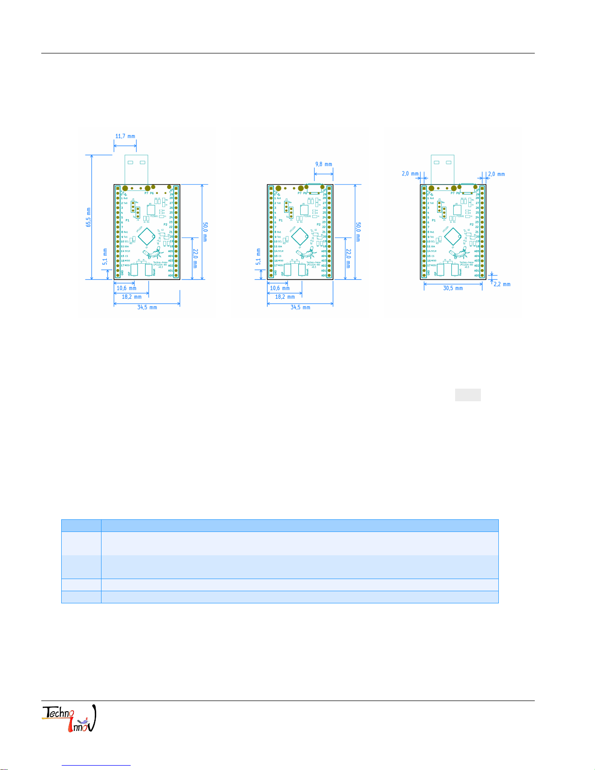
Fig 1 – USB A board type Fig 2 – micro USB board type Fig 3 – Headers (2.54mm)
Figures 1, 2 and 3 give the different dimensions and the position of the main elements (connectors, buttons and
user led) of the module.
The only difference between the "USB A" and the "micro USB board types is the USB connector.
Note : Not all components are shown on each figure for readability. All components but the USB
connector are the same on both board types.
3.2 Connectors
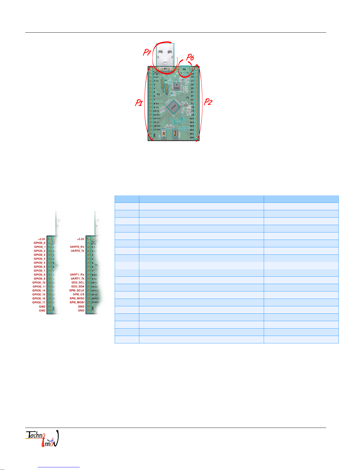
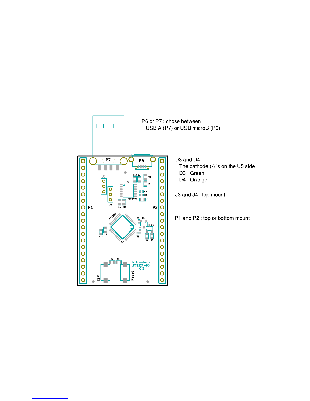
The module has two 2.54mm pitch headers numbered P1 and P2, and one USB connector, either P6 or P7
depending on the board type. Refer to figure 4 for connectors position and to table 1 for a short description.
Detailed description of the signals found on each connector pin follow.
Name Description
P1
P2
P6 USB micro-AB female connector. Available only on micro USB board type.
P7 USB A male connector. Available only on USB A board type.
19 pins, 2.54mm pitch header. Provides +3.3V, ground, UARTS, I2C, SPI, and GPIO from
port 0.
19 pins, 2.54mm pitch header. Provides +5V from USB, ADC, and GPIO from port 0 and
1.
Table 1 – Module Connectors Description
Techno-Innov - DomoTab
http://www.techno-innov.fr
page 5 / 22
Page 6
LPC1224_BO_SRM Board v0.3
Fig 4 – Module Connectors
3.2.1 P1 Connector
Pin # Description LPC Pin
1 +3.3V : +3.3 Volt 2 - LPC pin 15 : PIO0_0
3 Rx0 : LPC UART_0 Receive Data LPC pin 16 : PIO0_1
4 Tx0 : LPC UART_0 Transmit Data LPC pin 17 : PIO0_2
5 - LPC pin 18 : PIO0_3
6 - LPC pin 19 : PIO0_4
7 - LPC pin 20 : PIO0_5
8 - LPC pin 21 : PIO0_6
9 - LPC pin 22 : PIO0_7
10 Rx1 : LPC UART_1 Receive Data LPC pin 23 : PIO0_8
11 Tx1 : LPC UART_1 Transmit Data LPC pin 24 : PIO0_9
12 SCL : Clock for I2C bus LPC pin 25 : PIO0_10
13 SDA : Bidirectional Serial Data for I2C bus LPC pin 26 : PIO0_11
14 SCK : Clock for SPI bus LPC pin 29 : PIO0_14
15 SSEL : Slave Select for SPI bus LPC pin 30 : PIO0_15
16 MISO : Master In Slave Out for SPI bus LPC pin 31 : PIO0_16
Fig 5 – P1 Connector
17 MOSI : Master Out Slave In for SPI bus LPC pin 32 : PIO0_17
18 GND : Ground 19 GND : Ground -
P1 connector is a standard 2.54mm (0.1 inch) pitch header, with 1 row of 19 pins, and can be populated using
either male or female header, and mounted either on top or on bottom of the board.
P1 connector provides access to +3.3V, Ground, UART0, UART1, I2C, SPI, and additional GPIO pins from port
0 of the LPC micro-controller.
Table 2 – P1 Connector Pinout
Techno-Innov - DomoTab
http://www.techno-innov.fr
page 6 / 22
Page 7
LPC1224_BO_SRM Board v0.3
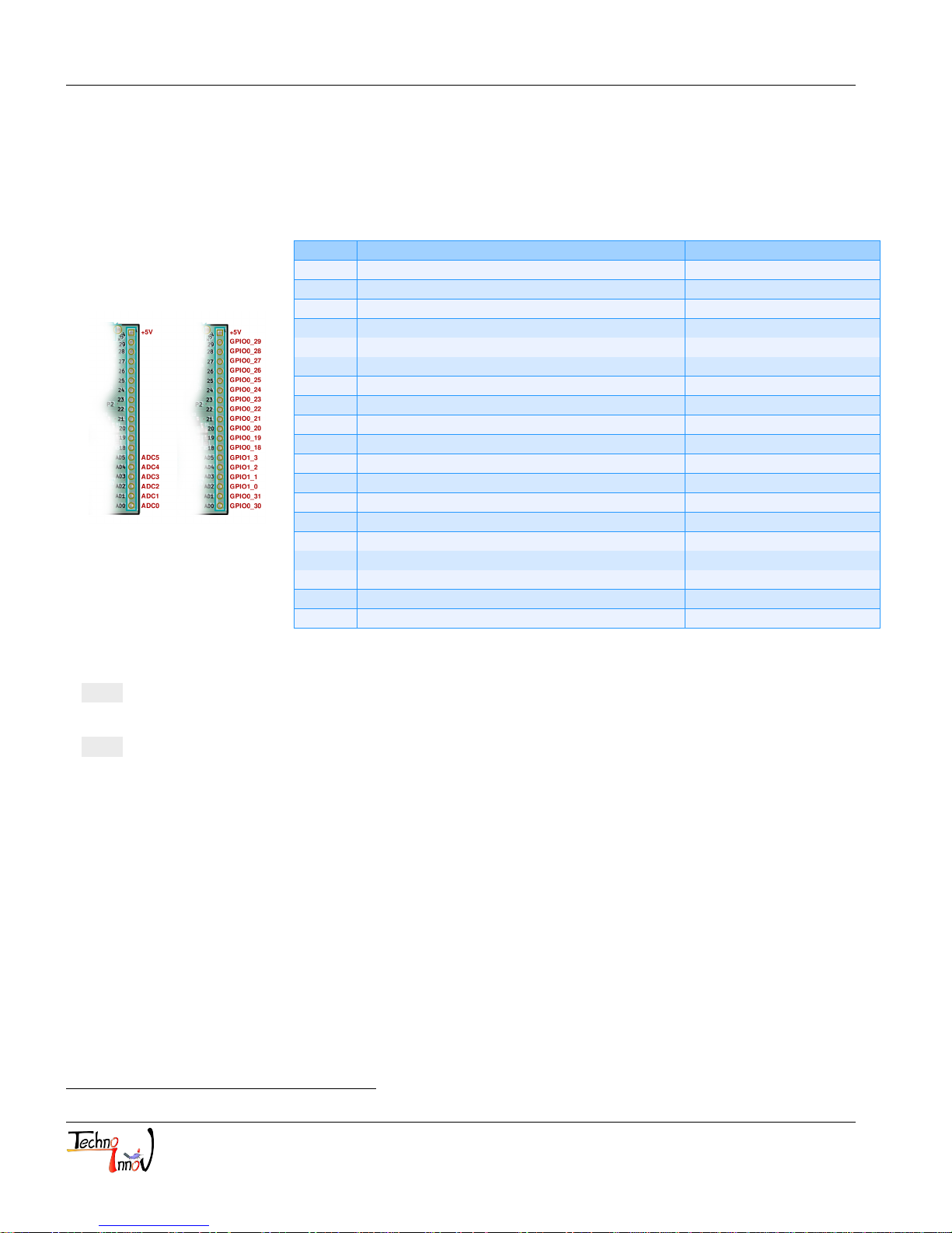
3.2.2 P2 Connector
P2 connector is a standard 2.54mm (0.1 inch) pitch header, with 1 row of 10 pins, and can be populated using
either male or female header, and mounted either on top or on bottom side of the board.
P2 connector provides access to USB +5V power supply, ADC, and GPIO pins from port 0 and 1 of the LPC
micro-controller.
Pin # Description LPC Pin
1 +5V : +5 Volt from USB connector 2 - LPC pin 14 : PIO0_29
3 - LPC pin 13 : PIO0_28
4 - LPC pin 12 : PIO0_27
5 - LPC pin 11 : PIO0_26
6 - LPC pin 10 : PIO0_25
7 - LPC pin 9 : PIO0_24
8 - LPC pin 8 : PIO0_23
9 - LPC pin 7 : PIO0_22
10 - LPC pin 6 : PIO0_21
11 - LPC pin 5 : PIO0_20
12 - LPC pin 4 : PIO0_19
13 - LPC pin 33 : PIO0_18
14 ADC5 LPC pin 39 : PIO1_3
Fig 6 – P2 Connector
15 ADC4 LPC pin 38 : PIO1_2
16 ADC3 LPC pin 37 : PIO1_1
17 ADC2 LPC pin 36 : PIO1_0
18 ADC1 LPC pin 35 : PIO0_31
19 ADC0 LPC pin 34 : PIO0_30
Table 3 – P2 Connector Pinout
Note : Most P2 pins also provide alternate capture or match input functions for 32-bit timers. Refer
to the LPC1224 documentation from NXP for full documentation of the alternate functions.
Note : When the board is not connected to a power source on the USB port the +5V is not present
on pin 1 of P2 connector.
3.2.3 P6 and P7 Connectors
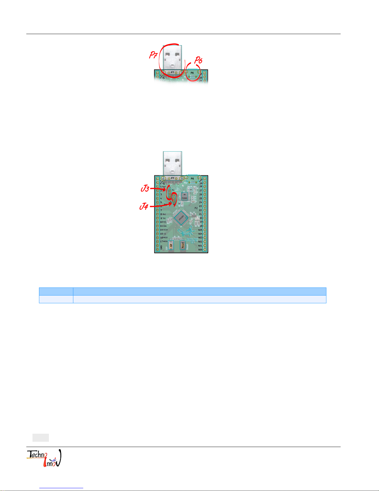
P6 and P7 are one-time choice options. Only one of them is present, depending on the board type. Both are
standard USB connectors. P6 is a female micro-AB port, and P7 is a male USB-A port.
Refer to the Universal Serial Bus (USB)2page on Wikipedia for pinout and more information on the USB bus and
connectors.
2. http://fr.wikipedia.org/wiki/Universal_Serial_Bus
Techno-Innov - DomoTab
http://www.techno-innov.fr
page 7 / 22
Page 8
LPC1224_BO_SRM Board v0.3
Fig 7 – P6 and P7 Connectors
3.3 Jumpers
The module has 2 configuration jumpers, numbered J3 and J4. Jumpers are common to all board types.
Fig 8 – Module Jumpers
Name Description
J3 and J4 Selection between UART0 andUART1 for USB-to-UART bridge.
Table 4 – Module Jumpers Description
3.3.1 J3 and J4 jumpers
J3 and J4 jumpers are used to connect UART0 or UART1 pins to the FTDI FT230XS USB-to-UART bridge.
When the jumpers are on the top two pins for each jumper, then UART0 is connected to the USB-to-UART
bridge. This position must be used for binary upload in ISP mode.
When the jumpers are on the bottom pins for each jumper, then UART1 is connected to the USB-to-UART
bridge.
It is possible to operate the board without jumpers. Then the UAS-to-UART is not connected to the microcontroller.
Note : It is not mandatory for the jumpers to be on the same position on J3 and J4.
Techno-Innov - DomoTab
http://www.techno-innov.fr
page 8 / 22
Page 9
LPC1224_BO_SRM Board v0.3
4 Electronics
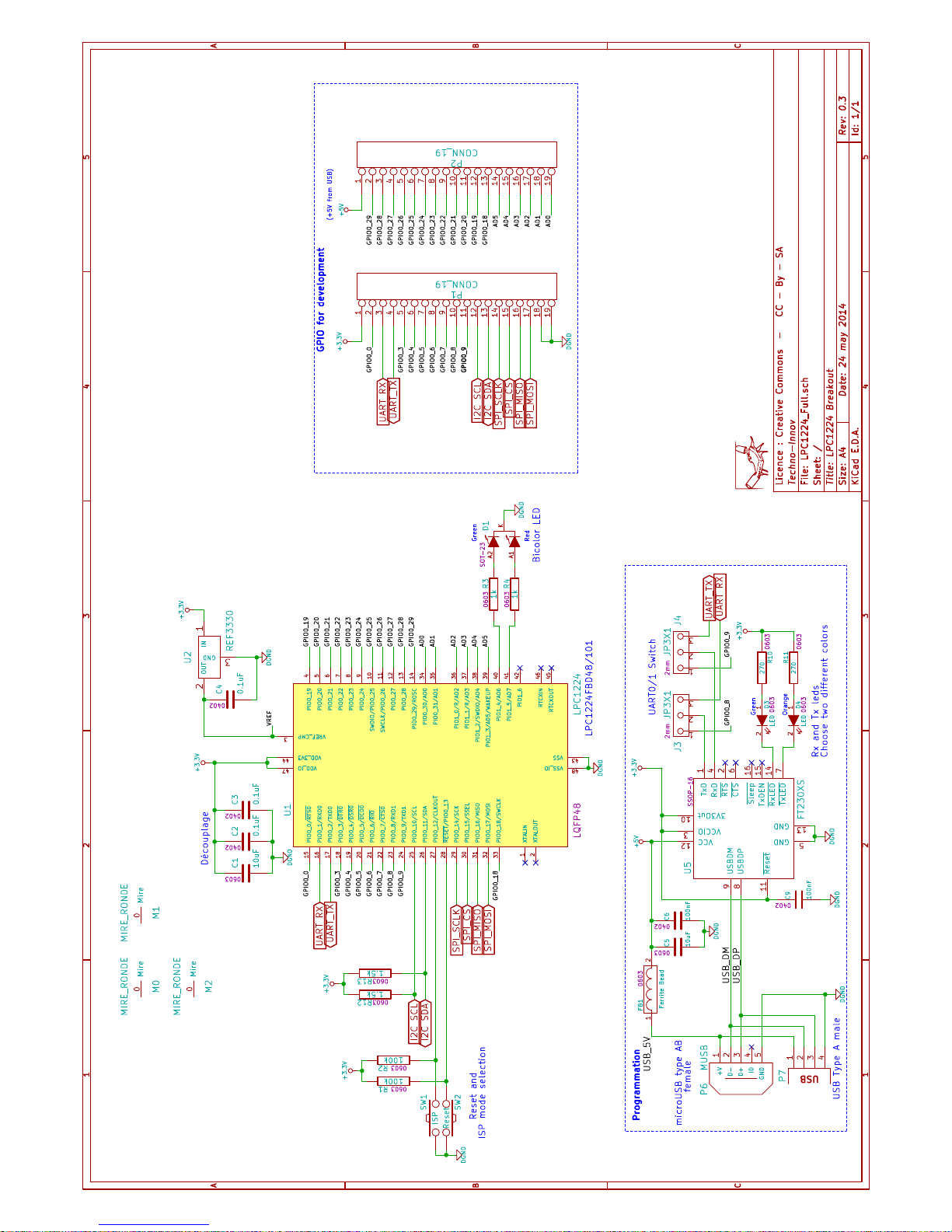
The LPC1224 break-out board has been created using KiCad3EDA software suite for the creation of the schematics and printed circuit boards.
See page 19 in the annexes for the full schematics. The sources for the schematics are available for download from
the module page4on Techno-Innov.fr.
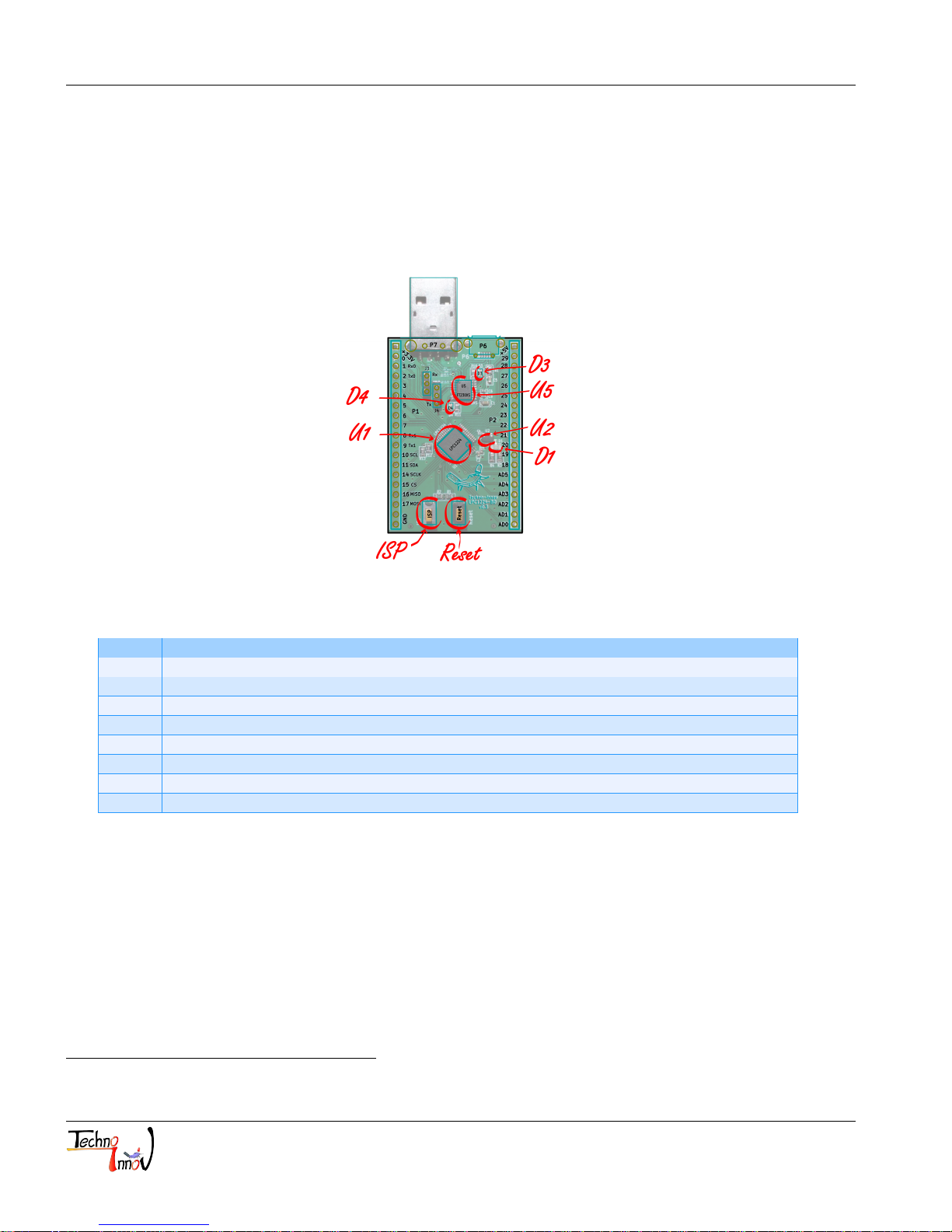
Fig 9 – Module Main Components
Name Description
U1 LPC1224 ARM Cortex-M0 micro-controller.
U2 3.0V LDO reference voltage generator.
U5 FTDI FT230XS USB to UART bridge.
D1 User led, bicolore (red / green).
D3 Green led : FTDI Rx activity.
D4 Orange led : FTDI Tx activity..
Reset Reset button for LPC1224 (SW2).
ISP ISP mode select button for LPC1224 (SW1).
Table 5 – Module Main Components Description
4.1 Micro-controller LPC1224
The module’s micro-controller is a LPC1224 from NXP5. The LPC1224 version used on the module is the
LPC1224FBD48/101. All LPC1224 have an ARM Cortex-M0 core running at up to 45 MHz.
The module uses the internal 12 MHz RC Oscillator as main clock. Its 1% accuracy is suitable for most applications.
3. http://www.kicad-pcb.org/display/KICAD/
4. http://www.techno-innov.fr/technique- lpc1224-bo/
5. http://www.nxp.com/products/microcontrollers/cortex_m0_m0/LPC1224FBD48.html
Techno-Innov - DomoTab
http://www.techno-innov.fr
page 9 / 22
Page 10
LPC1224_BO_SRM Board v0.3
Note : Refer to the LPC1224 documentation from NXP for full list and documentation of the LPC1224
features. Here are only the descriptions of the features used on the module.
4.1.1 Internal RAM
The LPC1224FBD48/101 has 4kB of internal SRAM mapped in one block at address 0x1000 0000.
4.1.2 Internal Flash
The LPC1224FBD48/101 has 32kB of internal FLASH memory, mapped at address 0x0000 0000. The flash memory programming requires no additional hardware thanks to the In-System Programming (ISP) and In-Application
Programming (IAP) on-chip bootloader software.
See section 4.1.6 (Reset and ISP mode) or sections 5.2 (Code Compilation) and 5.3 (Uploading binary on target)
for more information on internal FLASH memory.
4.1.3 Communication interfaces
The module makes use of the following communication interfaces found on the LPC1224 :
• Two UARTs : UART0 and UART1 are connected to P1 header and to the USB to UART bridge through
J3 and J4 jumpers.
UART0 is used for In-System Programming of the LPC1224.
• One I2C bus interface supporting full I2C-bus specification and Fast-mode Plus with a data rate of 1
Mbit/s. I2C is connected to P1 header. See section 4.2 for more information.
• One SSP/SPI controller with FIFO and multi-protocol capabilities. The SPI bus is also connected to P1
header.
4.1.4 GPIO
The module gives access to 34 GPIO pins dispatched on P1 and P2 connectors.
Refer to tables 2 and 3 for details of the signals available on these GPIO and to the LPC1224 documentation
from NXP for full list of features for each GPIO.
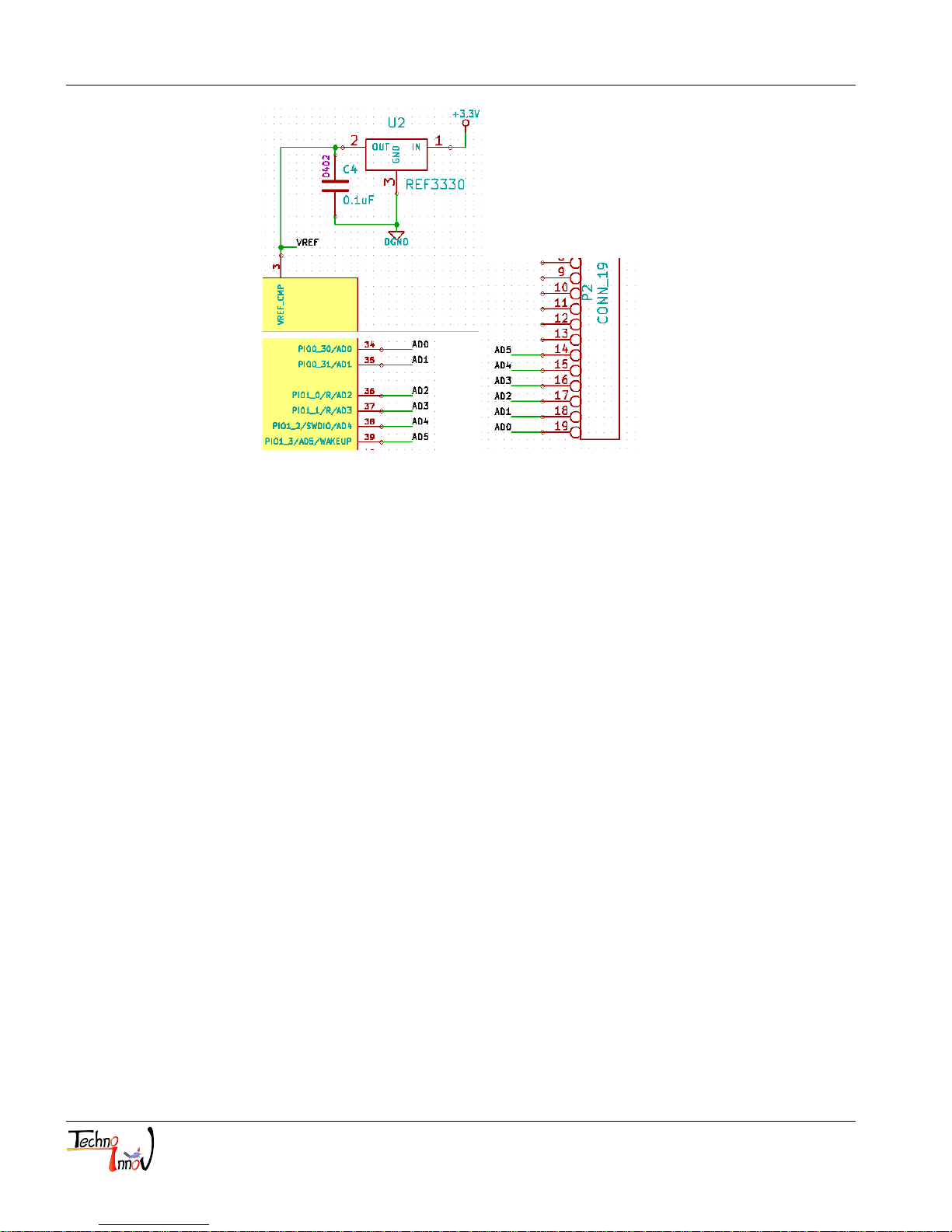
4.1.5 ADC
The last six GPIO pins on P2 connector are inputs channels 0 to 5 for the 10-bit ADC of the LPC1224 micro-
controller.
The internal ADC uses the voltage on the Vref pin as reference voltage for the conversion. The LPC1224 break-out
board integrates a 3.0V reference voltage LDO to provide a stable and accurate Vref to the LPC1224.
Techno-Innov - DomoTab
http://www.techno-innov.fr
page 10 / 22
Page 11
LPC1224_BO_SRM Board v0.3
Fig 10 – ADC Input Pins and Vref
4.1.6 Reset and ISP mode
Reseting the LPC1224 without removing the power can be done with the Reset button (SW2).
To enter In-System Programming (ISP) mode after reset you must hold the ISP button (SW1) when you release
the reset button. The LPC1224 bootloader considers a LOW level on the PIO0_12 pin as an external hardware
request to enter ISP mode and start the ISP command handler. The sampling of the GPIO0_12 pin may take up
to 3ms.
Refer to section 5.3 or to the LPC1224 user manual for more information on ISP mode.
If the ISP button is not held when th Reset button is released (and a valid user code is found in Flash memory)
then the execution is transfered to the user program.
4.2 I2C
The LPC1224 break-out board has no components on the I2C bus, leaving the whole address space available for
the user. The LPC1224 break-out board provides two 1.5kOhms pull-up resistors on both SDA and SCL lines.
4.3 User Led and Button
The module has three leds and two buttons. The two leds connected to the USB to UART bridge (D3 and D4)
and the Reset button have dedicated functions and cannot be assigned other functions.
The remaining led (D1) and button (ISP) can be used as the user wishes.
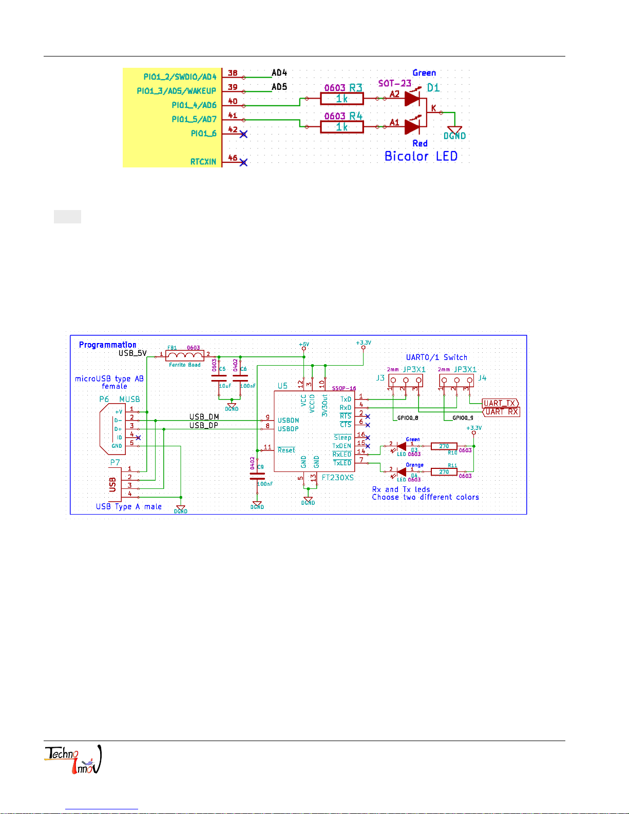
The D1 led is a bi-color red / green led connected to PIO1_4 (pin 40) and PIO1_5 (pin 41). Both can be turned
on at the same time, providing a third color (orange).
Techno-Innov - DomoTab
http://www.techno-innov.fr
page 11 / 22
Page 12
LPC1224_BO_SRM Board v0.3
Fig 11 – User Led
Note : The PIO1_4 and PIO1_5 pins are not PWM capable so it’s not possible to create shades
between red and green without using a lot of processing power.
After reset the ISP button can be used by the user to any purpose. It’s state can be read on pin PIO0_12 (pin
27).
4.4 USB to UART bridge
In order to ease the development process and the use of the module we added a USB to UART bridge on-board.
This bridge is made by a FTDI FT230XS chip. It provides a 3.3V regulated voltage for the module and is well
supported on most operating systems so there is usually no configuration required to use it as a serial line on the
host development system, removing the need of any additional power source or of specific hardware to program the
LPC1224 micro-controller and communicate with the module.
The FTDI chip controls two "activity" leds for Rx (D3, the green one) and Tx (D4, orange one) data over the
serial link.
Removing jumpers J3 and J4 disconnects the USB to UART bridge from the LPC1224 micro-controller.
Fig 12 – USB to UART bridge
Techno-Innov - DomoTab
http://www.techno-innov.fr
page 12 / 22
Page 13
LPC1224_BO_SRM Board v0.3
5 Software
The LPC micro-controller family uses ARM cores, which make them very easy to use. Apart from a few wrappers,
all the code can be written in C and compiled using gcc.
ARM, NXP and other vendors provide sample code, but published under many different licences. The code we
provide for the LPC1224 break-out board is published under the well known GPLv3 licence.
5.1 Sample Source Code
5.1.1 Grab the sources
An example application code can be downloaded from our git repository6using the following clone command :
user@host:˜/sw$ git clone http://gitclone.techno-innov.fr/modules
The LPC1224 break-out board can use the code from the apps/base sub-directory as there are very few
differences between the LPC1224 break-out board and the GPIO Demo module. The only differences are the lack
of EEPROM memory and temperature sensor on the I2C bus and the SPI CS pin which is not used for I2C clock
activation for the EEPROM and thus fully available to the user.
5.1.2 Sample code content
This code provides the micro-controller definitions (Cortex-M0 specific definitions, registers, interrupts ...) and
the routines required to start the micro-controller (bootstrap, vector table, power state, flash, clocks).
At the time of writing it also provides a basic set of library functions and the drivers for the interfaces found
on the module. The list of supported features and interfaces is updated as the development goes on, so read the
README file for the full list of supported features and interfaces.
The code has been split in five parts : core/ , drivers/ , extdrv/ , apps/ and lib/ (with the associated
directories under include/ for the headers) :
• core : Contains all the required parts and system initialisations. Many functions in there are defined as
weak aliases of dummy functions, so the code compiles even if no drivers are used. When these functions are
redefined in the driver code they override the weak definition.
• lib : Contains the implemented parts of the small C library for our code. The micro-controller does not run
a full Linux system, so the gnu libc must not be used, and even a µClibc is much more than what’s required.
Most of the code in these files come from the kernel implementations of libc parts.
• drivers : Contains the drivers for the different interfaces found on the module.
• extdrv : Provides drivers for external components, either on the module (EEPROM, status led, tmp101
temperature sensor), or to be purshased separately and connected to the module.
The number of external parts supported will grow with time. Note that it may not be possible to use all of
them at the same time.
• apps : Provides sample applications for the different modules made by Techno-Innov which demonstrate
either LPC1224 interfaces or external drivers, which can be used as base for your own developments.
Most modules will have their own directory under apps/ . The LPC1224 break-out board uses the base/
6. http://git.techno-innov.fr/?p=modules;a=summary
Techno-Innov - DomoTab
http://www.techno-innov.fr
page 13 / 22
Page 14
LPC1224_BO_SRM Board v0.3
subdirectory, which is common with the GPIO Demo module. Creating a new app is as easy as creating a new
sub-directory under apps/base (with no spaces or special caracters in the name), copying the Makefile
from one of the other apps in your new app directory, and creating your own C source file(s) (maybe starting
with a copy of an existing example).
If you created a new module, you should consider creating a new "module" directory under apps/ with it’s
own sub-directories for specific apps.
5.1.3 Sample code entry point
The main loop is in main.c in function main() , as with any C program, though main() is called by the
bootstrap code ( Reset_Handler() in core/bootstrap.c ) and could have any name.
The calls to the system initialisation routines have been put together in the system_init() function.
SELECTED_FREQ must be set to one of the FREQ_SEL_**MHz defined in include/core/system.h :
• FREQ_SEL_12MHz
• FREQ_SEL_24MHz
• FREQ_SEL_36MHz
• FREQ_SEL_48MHz
• FREQ_SEL_60MHz
Note : The frequency can go up to 60MHz despite what is said in the documentation, but the micro-
controller needs much more power at higher frequencies.
Note : system.h provides two sleep functions ( msleep() and usleep()). These will activate the
systick with a 1ms tick if it has not been done yet.
Note : usleep() may be very approximative for short usleep periods.
The pins used by your application should be configured using either the set_pins() function and pio_config
structures (see common_pins[] in most examples) or the config_gpio() function for each used pin.
5.2 Building the binary
5.2.1 Get a toolchain
Build has been tested using gcc, and only gcc, in the version provided by the Debian project7, but any ARM gcc
toolchain should do.
In order to get the Debian ARM gcc cross-toolchain you must install package gcc-arm-none-eabi .
There’s no need for the related libc package here, the libc does not fit in our micro-controller memory. Instead have
a look at the content of the lib/ directory, and add stuff there.
Alternatively you can download pre-compiled gcc toolchains (many different projects provide their own), or build
your own one using crosstool-ng8or similar projects. For more information on what is a (cross-)toolchain, have a
look at this information page on elinux.org9.
7. http://www.debian.org/
8. http://crosstool-ng.org/
9. http://elinux.org/Toolchains
Techno-Innov - DomoTab
http://www.techno-innov.fr
page 14 / 22
Page 15

LPC1224_BO_SRM Board v0.3
5.2.2 Build command and options
Once done with the toolchain installation (or if you already have one) you should build using the provided
Makefile by running the simple " make " command from any of the apps/base/ sub-directory.
You can also build all apps by running " make " from repository root directory or " make base/my_app " to compile
" my_app " from the apps/base/ sub-directory only. ( base may be replaced by any other module name). NoteYou
may want to change the CROSS_COMPILE variable from the main Makefile (in the repository root directory)
and set it to the prefix of your toolchain.
5.2.3 Build process
The specific information about the target (LPC1224 micro-controller) memory (Flash and RAM) used by the
linker is in the
lpc_link_lpc1224.ld linker script.
The vector table is defined in the core/bootstrap.c file, but the checksum of the first seven entries in the
vector table is left unmodified. This checksum must be computed and placed in the eighth vector entry as the
bootloader needs to find a valid checksum in the eighth entry to consider the user code as valid and transfer
execution to the reset handler (first vector table entry).
This is done by the lpcprog tool before sending the binary to the target.
5.3 Uploading binary on target
5.3.1 Tools
To flash the binary (the one with .bin) to the LPC Flash you can use our lpctools package, packaged for Debian
as of 2014-09-10 and available in jessie or newer versions, or available in the lpctools git repository10.
Lpctools is released under GPLv3 licence.
Clone the repository using :
user@host:˜/sw$ git clone http://gitclone.techno-innov.fr/lpctools
Then build ( make ) the tools.
Note : Other tools may be used but have not been tested. No tools were found to be open source when
we looked for tools to upload the binaries to the micro-controller. You must check that the tool you
chose to use can take care of the checksum computation.
5.3.2 Connection with target and upload
Usual command line to upload a binary to the micro-controller :
10. http://git.techno-innov.fr/lpctools
Techno-Innov - DomoTab
http://www.techno-innov.fr
page 15 / 22
Page 16
LPC1224_BO_SRM Board v0.3
user@host:˜/sw$ lpcprog -d /dev/ttyUSB0 -c flash mod_gpio.bin
Part ID 0x3640c02b found on line 18
Flash now all blank.
Checksum check OK
Flash size : 32768, trying to flash 8 blocks of 1024 bytes : 8192
Writing started, 8 blocks of 1024 bytes ...
user@host:˜/sw$
If you want to get information on the connected device use the id command of lpcprog :
user@host:˜/sw$ lpcprog -d /dev/ttyUSB0 -c id
Part ID 0x3640c02b found on line 18
Part ID is 0x3640c02b
UID: 0x1228f5f5 - 0x4b324307 - 0x08333834 - 0x4d7b2c1a
Boot code version is 1.6
user@host:˜/sw$
Note : The part information definition for each supported micro-controller is in the lpctools package.
See lpctools readme and lpcprog or lpcisp help (-h option) or manpages for more information.
6 Board revisions history
6.1 v01
This board revision has not been sold.
First prototype version, with Rx and Tx crossed for UART1, making it impossible to connect them to USB to
UART bridge.
6.2 v02
This board revision has not been sold.
Added 3.0V LDO voltage regulator for Vref.
6.3 v03
Actual version sold as of writting of this documentation.
Added a 100nF cap to Vref pin.
Techno-Innov - DomoTab
http://www.techno-innov.fr
page 16 / 22
Page 17
LPC1224_BO_SRM Board v0.3
7 Annexes
7.1 Schematics
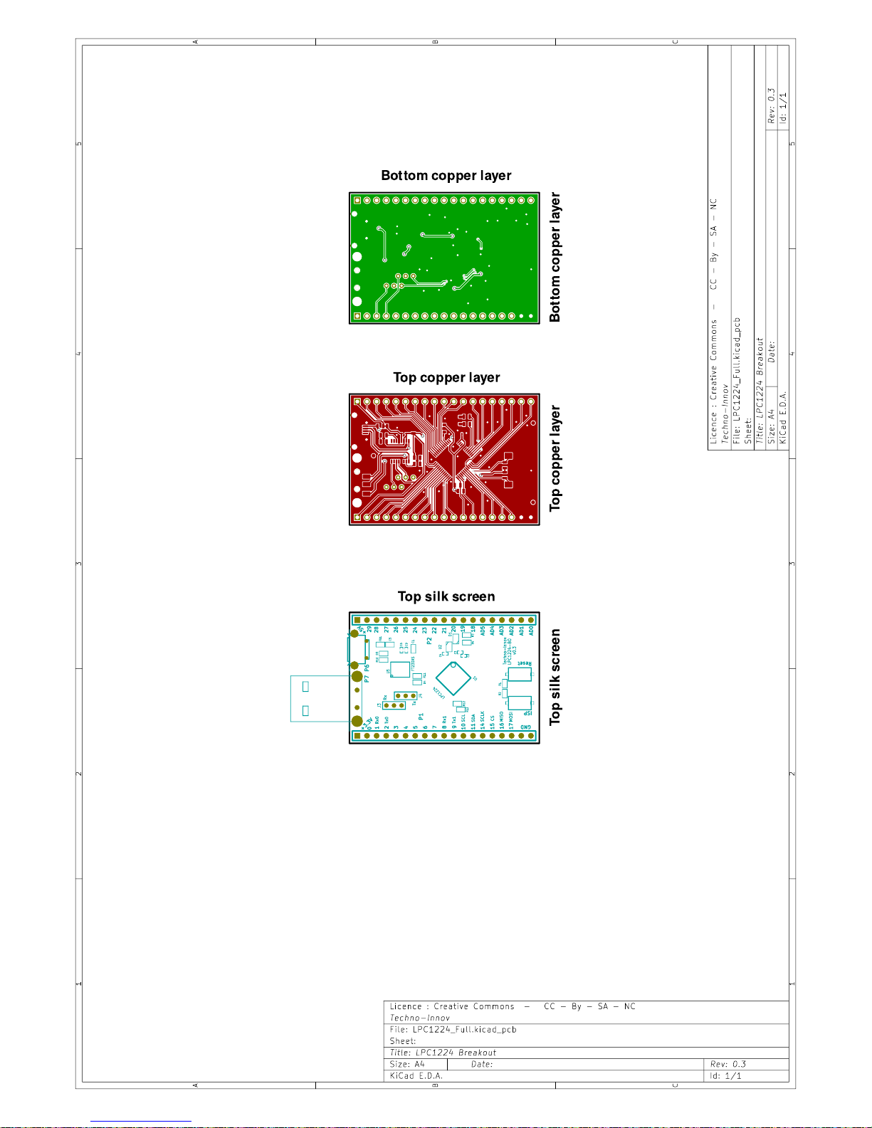
The board schematics and PCB layout have been created using KiCad11EDA software suite. You can download
the sources on the module page12on Techno-Innov.fr.
(See on next pages)
11. http://www.kicad-pcb.org/display/KICAD/
12. http://www.techno-innov.fr/technique- lpc1224-bo/
Techno-Innov - DomoTab
http://www.techno-innov.fr
page 17 / 22
Page 18
1
1
2
2
3
3
4
4
5
5
A A
B B
C C
Date: 24 may 2014
KiCad E.D.A.
Rev: 0.3Size: A4
Id: 1/1
Title: LPC1224 Breakout
File: LPC1224_Full.sch
Sheet: /
Techno-Innov
Licence : Creative Commons - CC - By - SA
GPIO for development
(+5V from USB)
GPIO0_8
+3,3V
DGND
+5V
AD1
AD2
AD3
AD5
AD4
AD0
GPIO0_19
GPIO0_20
GPIO0_21
GPIO0_24
GPIO0_23
GPIO0_22
GPIO0_28
GPIO0_29
GPIO0_27
GPIO0_26
GPIO0_25
GPIO0_0
GPIO0_9
GPIO0_3
GPIO0_6
GPIO0_5
GPIO0_4
Bicolor LED
Rx and Tx leds
Choose two different colors
microUSB type AB
female
USB Type A male
Découplage
Reset and
ISP mode selection
UART0/1 Switch
UART_TX
UART RX
1
2
3
J4
JP3X1
2mm
1
2
3
J3
JP3X1
2mm
R13
1.5k
0603
+3,3V
R12
1.5k
0603
VREF
+3,3V
+5V
AD0
AD4
AD5
AD3
AD2
AD1
GPIO0_4
GPIO0_5
GPIO0_6
GPIO0_9
GPIO0_8
GPIO0_3
GPIO0_0
GPIO0_25
GPIO0_26
GPIO0_27
GPIO0_29
GPIO0_28
GPIO0_22
GPIO0_23
GPIO0_24
GPIO0_21
GPIO0_20
GPIO0_19
XTALIN1XTALOUT
2
VREF_CMP
3
PIO0_194PIO0_205PIO0_216PIO0_227PIO0_238PIO0_24
9
SWDIO/PIO0_25
10
PIO0_5/DCD0
20
PIO0_15/SSEL
30
PIO1_4/AD6
40
SWCLK/PIO0_26
11
PIO0_6/RIO
21
PIO0_16/MISO
31
PIO1_5/AD7
41
PIO0_27
12
PIO0_7/CTS0
22
PIO0_17/MOSI
32
PIO1_6
42
PIO0_28
13
PIO0_8/RXD1
23
PIO0_18/SWCLK
33
VSS
43
PIO0_29/ROSC
14
PIO0_9/TXD1
24
PIO0_30/AD0
34
VDD_3V3
44
PIO0_0/RTS0
15
PIO0_10/SCL
25
PIO0_31/AD1
35
RTCXOUT
45
PIO0_1/RXD0
16
PIO0_11/SDA
26
PIO1_0/R/AD2
36
RTCXIN
46
PIO0_2/TXD0
17
PIO0_12/CLKOUT
27
PIO1_1/R/AD3
37
VDD_IO
47
PIO0_3/DTR0
18
RESET/PIO0_13
28
PIO1_2/SWDIO/AD4
38
VSS_IO
48
PIO0_4/DSR0
19
PIO0_14/SCK
29
PIO1_3/AD5/WAKEUP
39
U1
LPC1224LQFP48
I2C SDA
I2C SCL
Programmation
DGND
+3,3V
DGND
TxD
1
RTS
2
VCCIO
3
RxD
4
GND
5
CTS
6
TxLED
7
USBDP
8
USBDM
9
3V3Out
10
Reset
11
VCC
12
GND
13
RxLED
14
TxDEN
15
Sleep
16
U5
FT230XS
SSOP-16
C5
10uF
0603
C6
100nF
0402
C9
100nF
0402
DGND
1 2
FB1
Ferrite Bead
0603
+V
1D-2D+3ID4
GND
5
P6 MUSB
DGND
R10
270
0603
R11
270
0603
12
D3
LED 0603
+3,3V
12
D4
LED 0603
USB
123
4
P7
C2
0.1uF
0402
C3
0.1uF
0402
R4
1k
0603
R2
100k
0603
R1
100k
0603
SW2
Reset
SW1
ISP
Mire
0
M2
MIRE_RONDE
Mire
0
M1
MIRE_RONDE
Mire
0
M0
MIRE_RONDE
UART RX
UART_TX
LPC1224FBD48/101
+3,3V
SPI_MISO
SPI_CS
SPI_MOSI
SPI_SCLK
DGND
R3
1k
0603
DGND
K
A1
A2
D1
SOT-23
C1
10uF
0603
DGND
DGND
+3,3V
SPI_MOSI
SPI_SCLK
SPI_CS
UART RX
SPI_MISO
UART_TX
I2C SDA
I2C SCL
GPIO0_18
GPIO0_7
GPIO0_7
GPIO0_18
GPIO0_9
123456789
101112131415161718
19
P1
CONN_19
123456789
101112131415161718
19
P2
CONN_19
GPIO0_9GPIO0_8
IN
1
OUT
2
GND
3
U2
REF3330
DGND
USB_5V
USB_DM
USB_DP
Green
Orange
Green
Red
C4
0.1uF
0402
Page 19
Page 20
Page 21
LPC1224_BO_SRM Board v0.3
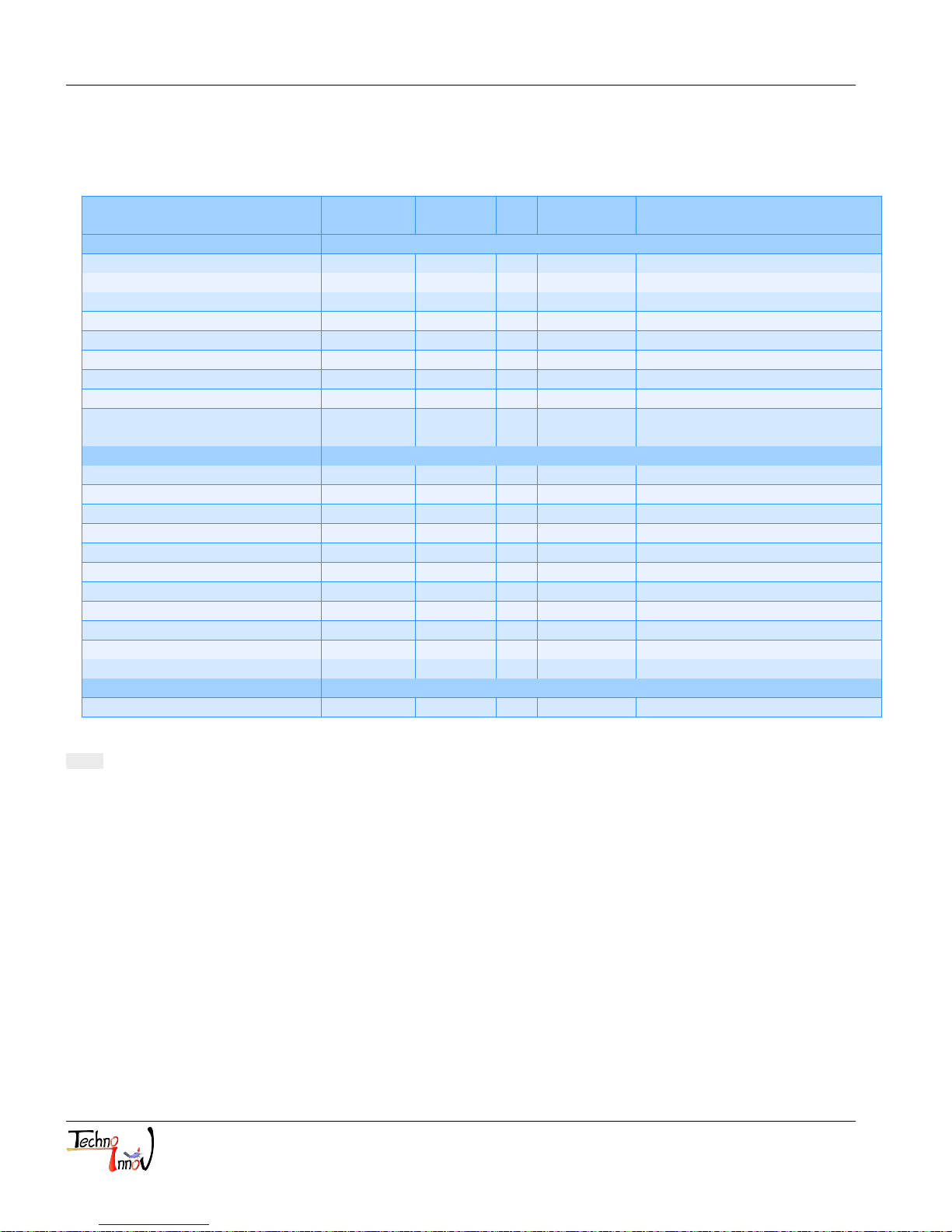
7.2 BOM
7.2.1 Block version
Part Description Ref Module Nb Vendor Vendor ref
Farnell
ref
Micro-controller
LPC1224 U1 LQFP48 1 NXP LPC1224FBD48/101 1862465
Decoupling capacitors 100nF C2, C3, C4 0402 3 Multicomp MCCA000050 1758896
Filter capacitor 10µF C1 0603 1 TDK C1608X5R0J106M 2112705
Pull-Up resistors 100k Ohms R1, R2 0603 2 Multicomp MC0063W06031%100K 9330402
I2C Pull-Up resistors 1,5k Ohms R12, R13 0603 2 Multicomp MC0063W06031%1K5 9330607
Bi-color Led resistors 270 Ohms R3, R4 0603 2 Multicomp MC0063W06031%270R 9330917
SMD Led Red / Green D1 SOT-23 1 Kingbright KM-23ESGW 1142614
SMD switchs SW1, SW2 2 Multicomp DTSM-32S-B 9471898
3.0V Vref U2 SOT-23 1
Texas Instrument
REF3330AIDBZT 1755084
USB Bridge
Led resistors 270 Ohms R10, R11 0603 2 Multicomp MC0063W06031%270R 9330917
Decoupling capacitors 100nF C6, C9 0402 2 Multicomp MCCA000050 1758896
Filter capacitor 10µF C5 0603 1 TDK C1608X5R0J106M 2112705
SMD chip bead FB1 0603 1 TDK MMZ1608R601A 1669700
Rx Led - Green D3 0603 1 Vishay VLMG1300-GS08 2251461
Tx Led - Orange D4 0603 1 Vishay VLMO1300-GS08 2251473
FT230XS USB to UART U5 16SSOP 1 FTDI FT230XS 2081321
Micro-USB type A-B female P6 SMD 1 Molex 47590-0001 1568022
USB Type A male P7 SMD 1 Multicomp MC32605 1696546
Male headers 1x3 J3, J4 2mm 2 Fisher SLY1.085.50G 9729135
Jumpers 2mm black 2 Harwin M22-1900005 510932
GPIO Connectors
Male headers GPIO (2 x 19 pins) P1, P2 2,54mm 2 Fischer SL1.025.36Z 9729038
Table 6 – BOM by functional block
Note : Components used on Board may change for functionnally equivalent references without prior
notice
Techno-Innov - DomoTab
http://www.techno-innov.fr
page 21 / 22
Page 22
LPC1224_BO_SRM Board v0.3
7.2.2 Easy order version
Part Description Ref Module Nb Vendor Vendor ref
LPC1224 U1 LQFP48 1 NXP LPC1224FBD48/101 1862465
FT230XS USB to UART U5 16SSOP 1 FTDI FT230XS 2081321
SMD chip bead FB1 0603 1 TDK MMZ1608R601A 1669700
Decoupling capacitors 100nF
C2, C3,
C4, C6, C9
0402 5 Multicomp MCCA000050 1758896
Filter capacitor 10µF C1, C5 0603 2 TDK C1608X5R0J106M 2112705
Pull-Up resistors 100k Ohms R1, R2 0603 2 Multicomp MC0063W06031%100K 9330402
I2C Pull-Up resistors 1,5k Ohms R12, R13 0603 2 Multicomp MC0063W06031%1K5 9330607
Led resistors 270 Ohms
R3, R4,
R10, R11
0603 4 Multicomp MC0063W06031%270R 9330917
SMD Led Red / Green D1 SOT-23 1 Kingbright KM-23ESGW 1142614
Rx Led - Green D3 0603 1 Vishay VLMG1300-GS08 2251461
Tx Led - Orange D4 0603 1 Vishay VLMO1300-GS08 2251473
SMD switchs SW1, SW2 2 Multicomp DTSM-32S-B 9471898
Micro-USB type A-B female P6 SMD 1 Molex 47590-0001 1568022
USB Type A male P7 SMD 1 Multicomp MC32605 1696546
Male headers 1x3 J3, J4 2mm 2 Fisher SLY1.085.50G 9729135
Jumpers 2mm black 2 Harwin M22-1900005 510932
Male headers GPIO (2 x 19 pins) P1, P2 2,54mm 2 Fischer SL1.025.36Z 9729038
Table 7 – BOM by reference
Note : Components used on Board may change for functionnally equivalent references without prior
notice
Farnell
ref
7.3 Document revision History
Version Date Author Information
0.3a April 12, 2015 Nathaël Pajani Initial revision
0.3b September 10, 2015 Nathaël Pajani
Changes according to code organisation modifications
7.4 Disclaimer
The LPC1224 break-out board is provided "as is" without warranty of any kind, either expressed or implied,
including, but not limited to, the implied warranties of merchantability and fitness for a particular purpose. The
entire risk as to the quality and performance of the LPC1224 break-out board is with you. Should the LPC1224
break-out board prove defective, you assume the cost of all necessary servicing, repair or correction.
Techno-Innov - DomoTab
http://www.techno-innov.fr
page 22 / 22
 Loading...