

Page 1

Navigator
Table Of Contents
file:///E|/_MANUALS/TECHNICS/technics_sl-pd7nasvc_[ET]/NA/SL-PD7/SVC/navigator.html[30/09/2009 12:13:01]
Page 2

Table Of Contents
COVER
1 Safety Precaution
2 Before Repair and Adjustment
3 Handling Precautions For Traverse Deck
4 Precaution of Laser Diode
5 Protection Circuitry
6 Accessories
7 Front Panel Controls
7.1 Front Panel
8 Operation Checks and Main Component Replacement Procedures
8.1 Checking Procedure for each major P.C.B.
9 Self-Diagnostic Display Function
10 Type Illustrations of ICs, Transistors& Diodes
11 Terminal Functions of ICs
11.1 IC701 (AN8885SBE1) Servo Amplifier
11.2 IC702 (MN662790RSC) Servo processor/ Digital signal processor/ Digital filter/ D/A converter
11.3 IC703 (AN8739SBE2) Focus coil/ Tracking coil/ Traverse motor/ Spindle motor driver
11.4 IC401 (C2BBGD000075) Microprocessor
12 Block Diagram
13 Schematic Diagram
14 Printed Circuit Board
15 Troubleshooting Guide
16 Wiring Connection Diagram
17 Parts Location and Replacement Parts List
17.1 CD Loading Mechanism
17.1.1 CD Loading Mechanism Part Location
17.1.2 CD Loading Mechanism Part List
17.2 Cabinet
file:///E|/_MANUALS/TECHNICS/technics_sl-pd7nasvc_[ET]/NA/SL-PD7/SVC/slpd7p.html[30/09/2009 12:13:32]
Page 3

17.2.1 Cabinet Parts Location
17.2.2 Cabinet Parts List
17.3 Electrical Parts List
17.4 Packing Materials& Accessories Parts List
17.5 Packaging
file:///E|/_MANUALS/TECHNICS/technics_sl-pd7nasvc_[ET]/NA/SL-PD7/SVC/slpd7p.html[30/09/2009 12:13:32]
Page 4
Service Manual
TOP NEXT
Order No. MD0102030C1
A2
Compact Disc Changer
SL-PD7
Colour
(K) ... Black Type
P ... U.S.A.
PC ... Canada
TRAVERSE DECK
RAE0152Z-3 Mechanism Series
AUDIO
No. of channels 2 (left and right, stereo)
Frequency response 2-20000 Hz,±1 dB
Output voltage 2V (at 0 dB)
Dynamic range 92 dB
S/N 100 dB
Total harmonic distortion 0.007% (1kHz, 0 dB)
Wow and flutter Below measurable limit
DA converter MASH (1 bit)
Output impedance Approx. 1kO
Load impedance More than 10 kO
PICKUP
Wavelength 780 nm
GENERAL
file:///E|/_MANUALS/TECHNICS/technics_sl-pd7nasvc_[ET]/NA/SL-PD7/SVC/s0000000000.html[30/09/2009 12:14:24]
Page 5
Power supply AC 120 V, 60 Hz
Power consumption 9 W
Dimensions (W x H x D) 430 x 125 x 374 mm
Mass 4.5 kg (9.9 lb.)
Power consumption in standby mode: 1 W
Notes:
1. Specifications are subject to change without notice./Mass and dimensions are approximate.
(16- 15/16” x 4- 29/32” x 14-23/32”)
© 2001 Matsushita Electronics (S) Pte. Ltd. All rights reserved. Unauthorized copying and distribution is a
violation of law.
TOP NEXT
file:///E|/_MANUALS/TECHNICS/technics_sl-pd7nasvc_[ET]/NA/SL-PD7/SVC/s0000000000.html[30/09/2009 12:14:24]
Page 6
1 Safety Precaution
TOP PREVIOUS NEXT
(This “Safety Precaution” is applied only in U.S.A.)
1. Before servicing, unplug the power cord to prevent an electric shock.
2. When replacing parts, use only manufacturer’s recommended components for safety.
3. Check the condition of the power cord. Replace if wear or damage is evident.
4. After servicing, be sure to restore the lead dress, insulation barriers, insulation papers, shields, etc.
5. Before returning the serviced equipment to the customer, be sure to make the following insulation resistance
test to prevent the customer from being exposed to a shock hazard.
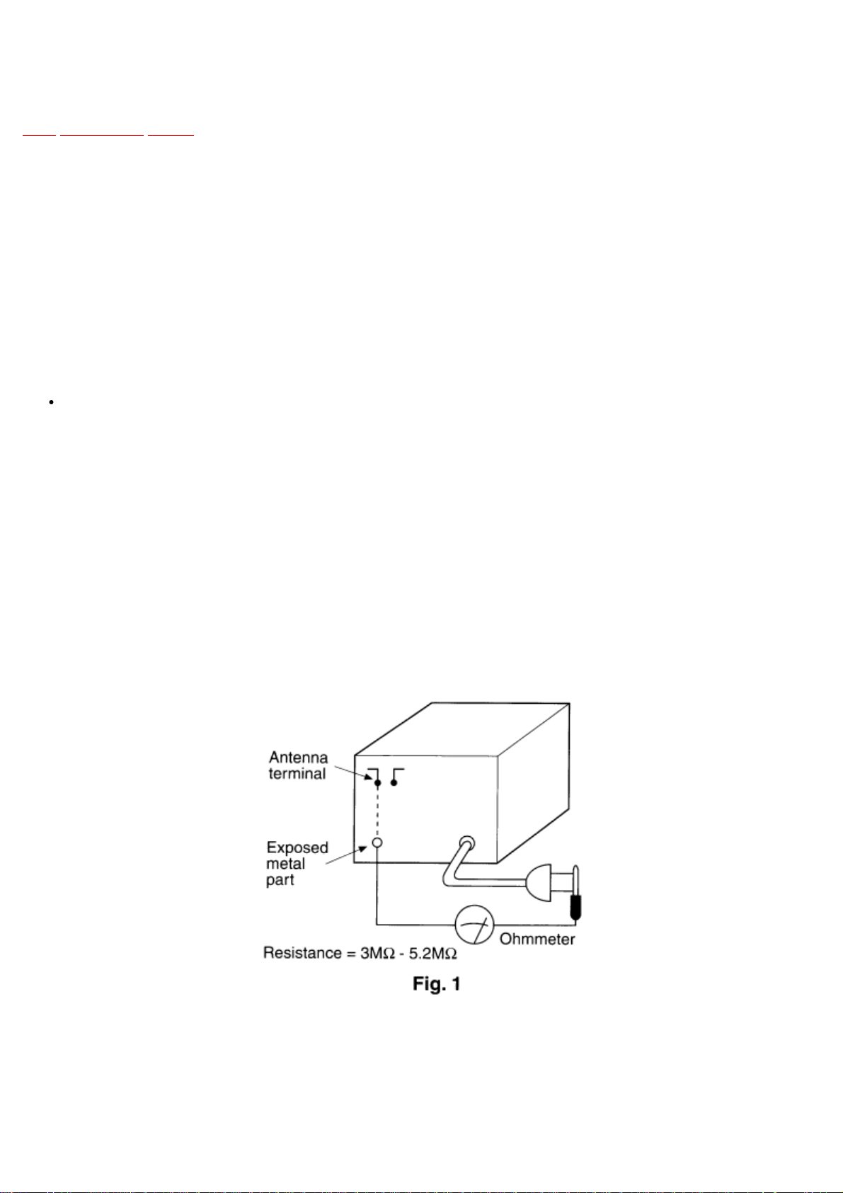
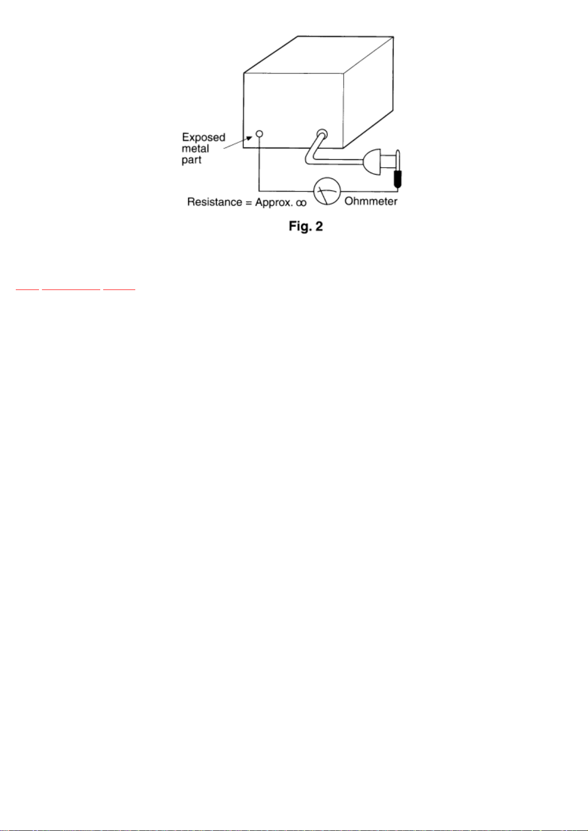
Insulation Resistance Test
1. Unplug the power cord and short the two prongs of the plug with a jumper wire.
2. Turn on the power switch.
3. Measure the resistance value with ohmmeter between the jumper AC plug and each exposed metal cabinet
part, such as screw heads, antenna, control shafts, handle brackets, etc. Equipment with antenna terminals
should read between 3MO and 5.2MO toall exposed parts*. (Fig 1) Equipment without antenna terminals
should read approximately infinity to all exposed parts. (Fig 2)
*Note: Some exposed parts may be isolated from the chassis by design. These will read infinity.
4. If the measurement is outside the specified limits, there is a possibility of a shock hazard. The equipment
should be repaired and rechecked before it is returned to the customer.
file:///E|/_MANUALS/TECHNICS/technics_sl-pd7nasvc_[ET]/NA/SL-PD7/SVC/s0100000000x.html[30/09/2009 12:14:25]
Page 7
TOP PREVIOUS NEXT
file:///E|/_MANUALS/TECHNICS/technics_sl-pd7nasvc_[ET]/NA/SL-PD7/SVC/s0100000000x.html[30/09/2009 12:14:25]
Page 8

2 Before Repair and Adjustment
TOP PREVIOUS NEXT
Disconnect AC power, discharge Power Supply Capacitors C12 through a 10 O, 5 W resistor to ground. DO NOT
SHORT-CIRCUIT DIRECTLY (with a screw driver blade, for instance), as this may destroy solid state devices.
After repairs are completed, restore power gradually using a variac, to avoid over current.
Current consumption at AC 120 V, 50 Hz and 60 Hz in NO SIGNAL mode should be 50~130 mA and 40~80 mA
respectively.
TOP PREVIOUS NEXT
file:///E|/_MANUALS/TECHNICS/technics_sl-pd7nasvc_[ET]/NA/SL-PD7/SVC/s0200000000x.html[30/09/2009 12:14:25]
Page 9
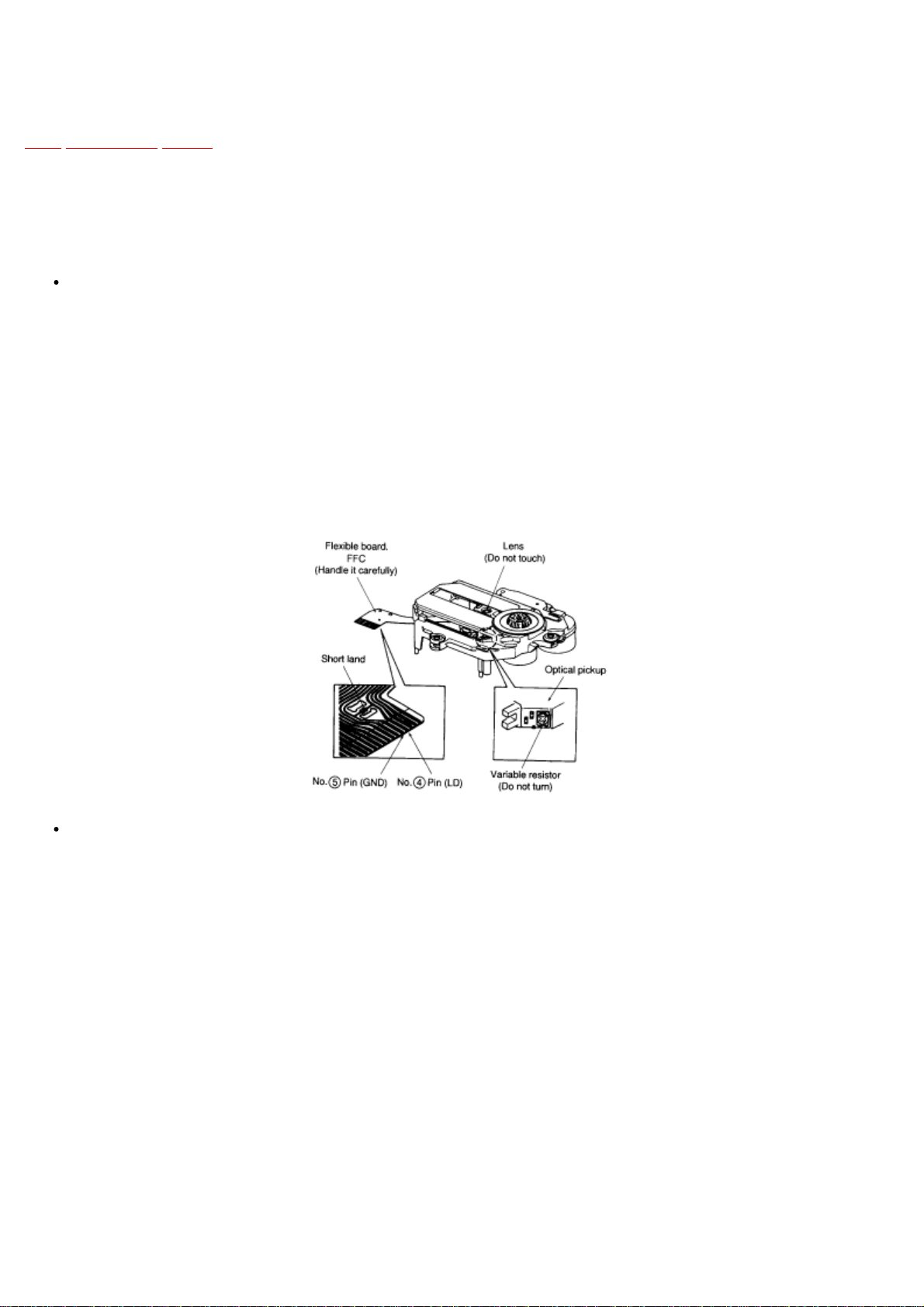
3 Handling Precautions For Traverse Deck
TOP PREVIOUS NEXT
The laser diode in the traverse deck (optical pickup) may break down due to potential difference caused by static
electricity of clothes or human body.
So, be careful of electrostatic breakdown during repair of the traverse deck (optical pickup).
Handling of traverse deck (optical pickup)
1. Do not subject the traverse deck (optical pickup) to static electricity as it is extremely sensitive to electrical
shock.
2. The short land between the No.4(LD) and No.5(GND) pins on the flexible board (FFC) is shorted with a
solder build-up to prevent damage to the laser diode.To connect to the PC board, be sure to open by
removing the solder build-up, and finishthe work quickly.
3. Take care not to apply excessive stress to the flexible board (FFC).
4. Do not turn the variable resistor (laser power adjustment). It has already been adjusted.
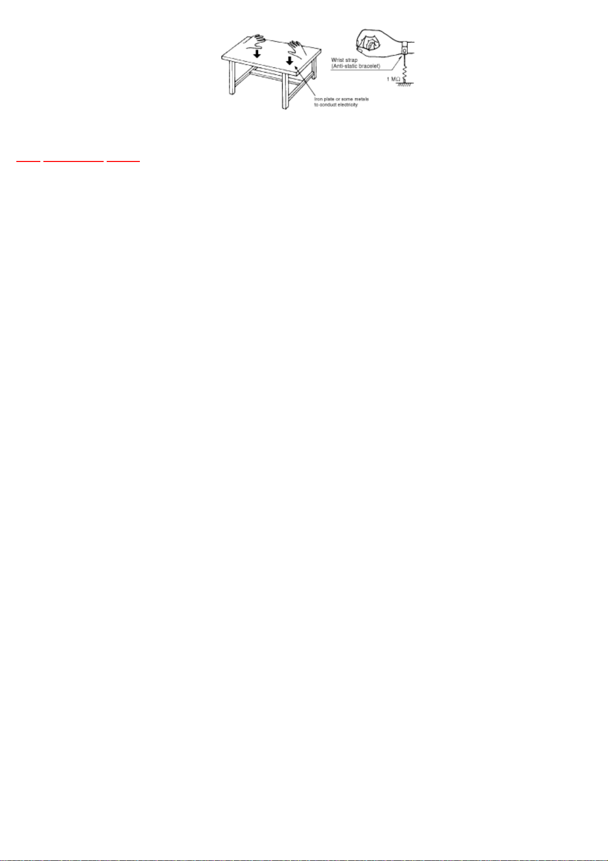
Grounding for electrostatic breakdown prevention
1. Human body grounding
Use the anti-static wrist strap to discharge the static electricity from your body.
2. Work table grounding
Put a conductive material (sheet) or steel sheet on the area where the traverse deck (optical pickup) is
placed, and ground the sheet.
Caution:
The static electricity of your clothes will not be grounded through the wrist strap. So, take care not to let your
clothes touch the traverse deck (optical pickup).
Caution when Replacing the Traverse Deck:
The traverse deck has a short point shorted with solder to protect the laser diode against electrostatics
breakdown. Be sure to remove the solder from the short point before making connections.
file:///E|/_MANUALS/TECHNICS/technics_sl-pd7nasvc_[ET]/NA/SL-PD7/SVC/s0300000000x.html[30/09/2009 12:14:26]
Page 10
TOP PREVIOUS NEXT
file:///E|/_MANUALS/TECHNICS/technics_sl-pd7nasvc_[ET]/NA/SL-PD7/SVC/s0300000000x.html[30/09/2009 12:14:26]
Page 11

4 Precaution of Laser Diode
TOP PREVIOUS NEXT
Caution:
This unit utilizes a class 1 laser. Invisible laser radiation is emitted from the optical pickup lens. When the unit is
turned on:
1. Do not look directly into the pickup lens.
2. Do not use optical instruments to look at the pickup lens.
3. Do not adjust the preset variable resistor on the pickup lens.
4. Do not disassemble the optical pickup unit.
5. If the optical pickup is replaced, use the manufacturer’s specified replacement pickup only.
6. Use of control or adjustments or performance of procedures other than those specified herein may result in
hazardous radiation exposure.
CAUTION!
THIS PRODUCT UTILIZES A LASER.
USE OF CONTROLS OR ADJUSTMENTS OR PERFORMANCE OF PROCEDURES OTHER THAN THOSE
SPECIFIED HEREIN MAY RESULT IN HAZARDOUS RADIATION EXPOSURE.
TOP PREVIOUS NEXT
file:///E|/_MANUALS/TECHNICS/technics_sl-pd7nasvc_[ET]/NA/SL-PD7/SVC/s0400000000x.html[30/09/2009 12:14:26]
Page 12

5 Protection Circuitry
TOP PREVIOUS NEXT
The protection circuitry may have operated if either of the following conditions are noticed:
No sound is heard when the power is turned on.
Stops during a performance.
The function of this circuitry is to prevent circuitry damage if, for example, the positive and negative speaker
connection wires are “shorted”, or if speaker systems with an impedance less than the indicated rated impedance
ofthe amplifier are used.
If this occurs, follow the procedure outlines below:
1. Turn off the power.
2. Determine the cause of the problem and correct it.
3. Turn on the power once again after one minute.
Note:
When the protection circuitry functions, the unit will not operate unless the power is first turned off and then on
again.
TOP PREVIOUS NEXT
file:///E|/_MANUALS/TECHNICS/technics_sl-pd7nasvc_[ET]/NA/SL-PD7/SVC/s0500000000x.html[30/09/2009 12:14:27]
Page 13
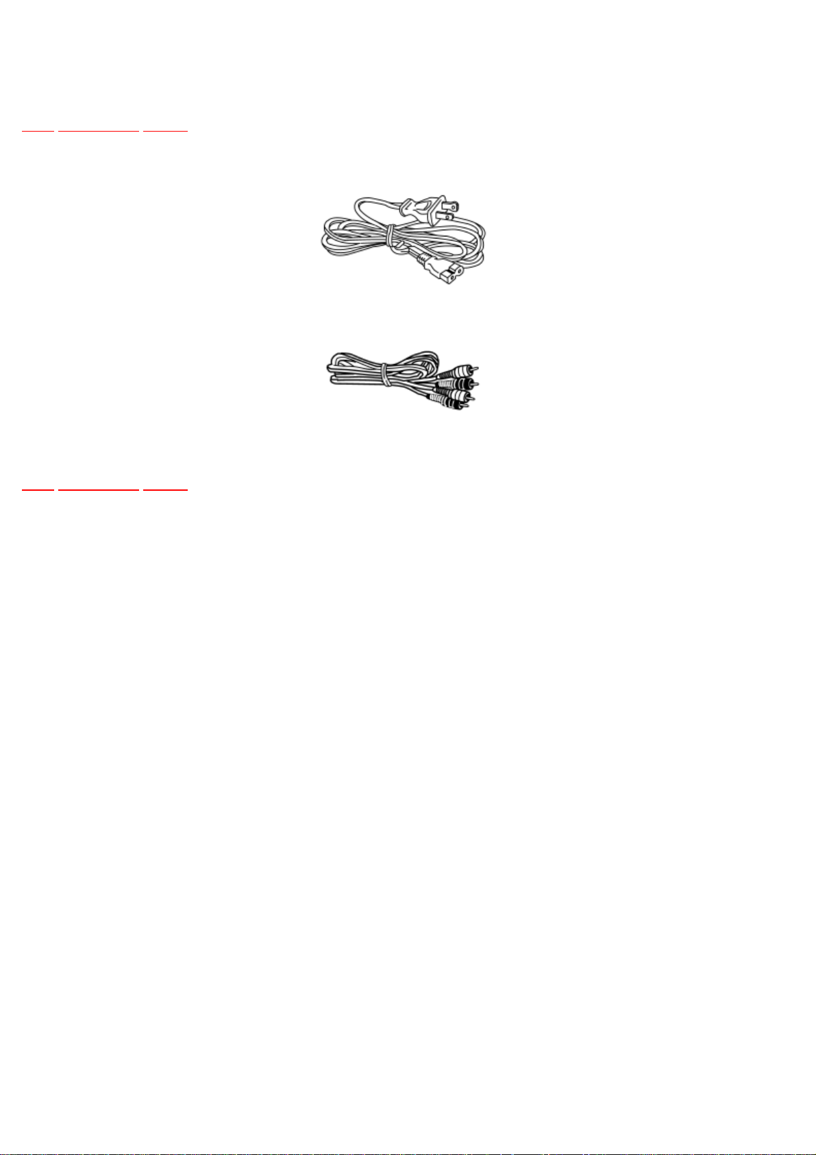
6 Accessories
TOP PREVIOUS NEXT
AC power supply cord... 1 pc.
Stereo connection cable... 1 pc.
TOP PREVIOUS NEXT
file:///E|/_MANUALS/TECHNICS/technics_sl-pd7nasvc_[ET]/NA/SL-PD7/SVC/s0600000000x.html[30/09/2009 12:14:27]
Page 14

7 Front Panel Controls
TOP PREVIOUS NEXT
7.1 Front Panel
TOP PREVIOUS NEXT
file:///E|/_MANUALS/TECHNICS/technics_sl-pd7nasvc_[ET]/NA/SL-PD7/SVC/s0700000000x.html[30/09/2009 12:14:28]
Page 15
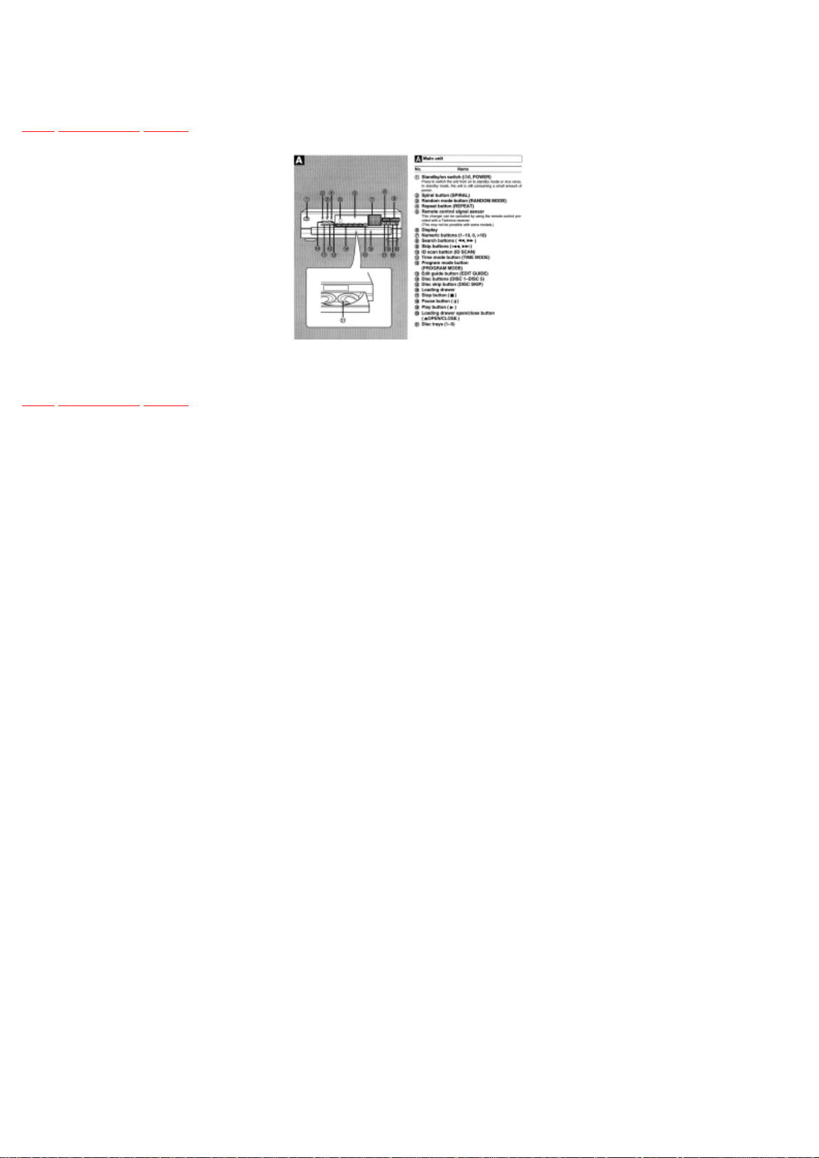
7.1 Front Panel
TOP PREVIOUS NEXT
TOP PREVIOUS NEXT
file:///E|/_MANUALS/TECHNICS/technics_sl-pd7nasvc_[ET]/NA/SL-PD7/SVC/s0701000000.html[30/09/2009 12:14:28]
Page 16

8 Operation Checks and Main Component
Replacement Procedures
TOP PREVIOUS NEXT
“ATTENTION SERVICER”
Some chassis components maybe have sharp edges. Be careful when diassembling and servicing.
1. This section describes procedures for checking the operation of the major printed circuit boards and replacing
the main components.
2. For reassembly after operation checks or replacement, reverse the respective procedures./Special reassembly
procedures are described only when required.
3. Select items from the following index when checks or replacement are required.
Content
Checking Procedure for each major P.C.B.
.................................................................................................................. P.g. 7~9
8.1 Checking Procedure for each major P.C.B.
TOP PREVIOUS NEXT
file:///E|/_MANUALS/TECHNICS/technics_sl-pd7nasvc_[ET]/NA/SL-PD7/SVC/s0800000000x.html[30/09/2009 12:14:29]
Page 17
8.1 Checking Procedure for each major P.C.B.
TOP PREVIOUS NEXT
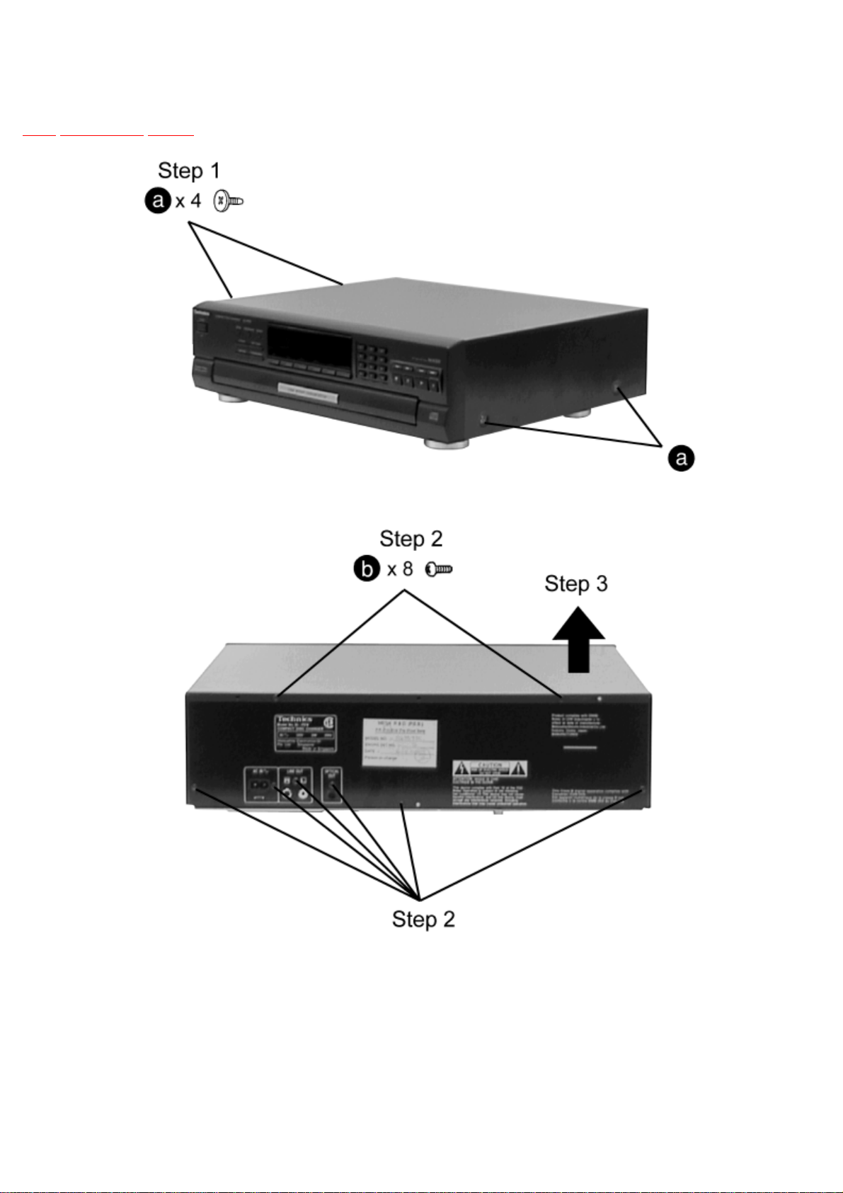
Step 1 Remove all the screws.
Step 3 Remove all the screws and remove top cabinet as shown.
file:///E|/_MANUALS/TECHNICS/technics_sl-pd7nasvc_[ET]/NA/SL-PD7/SVC/s0801000000.html[30/09/2009 12:14:30]
Page 18
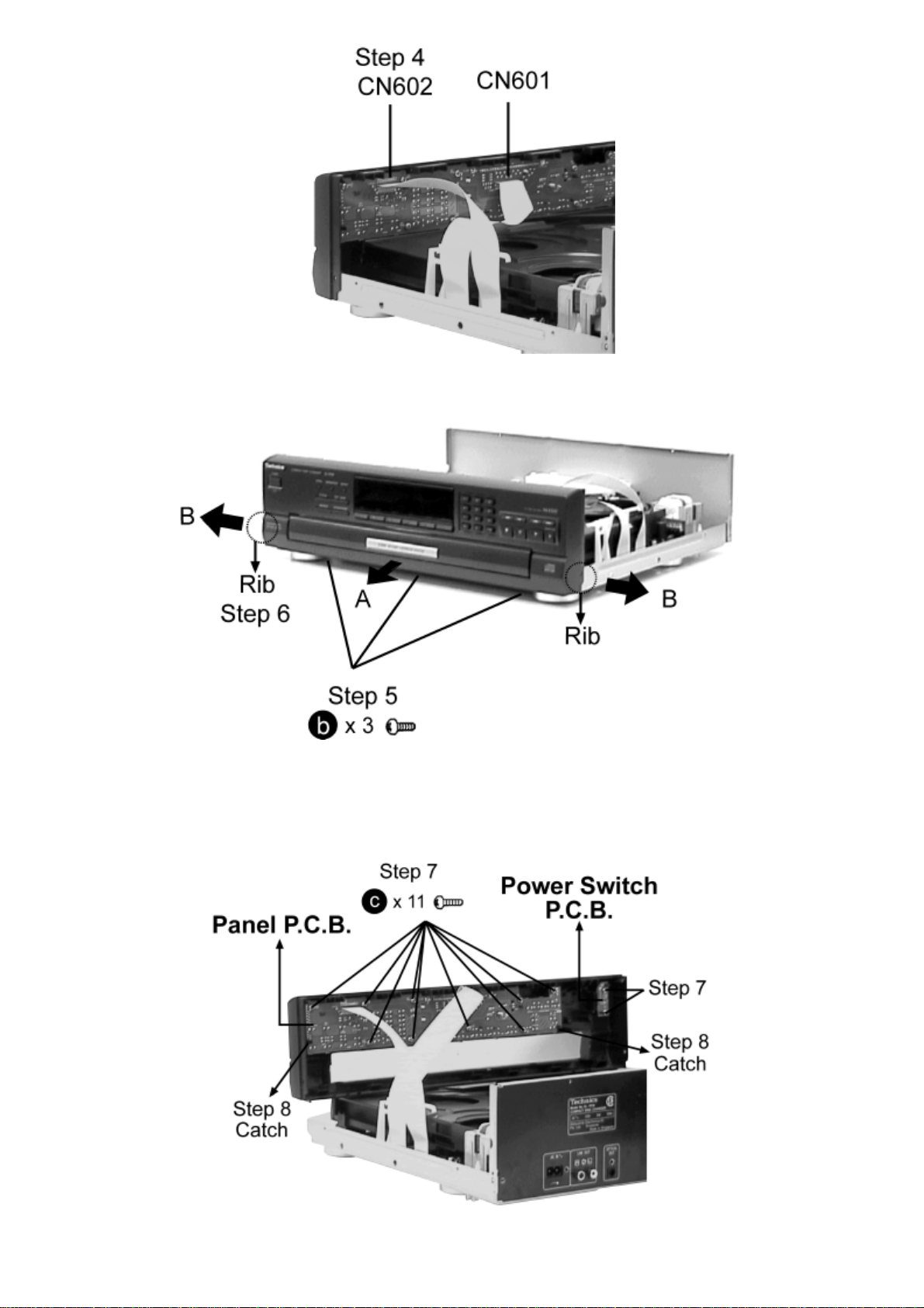
Step 4 Release the connectors CN601 and CN602.
Step 5 Remove all the screws.
Step 6 Pull the front panel in both direction of arrow B to unlock the rib and then remove the front in the direction
of arrow A.
file:///E|/_MANUALS/TECHNICS/technics_sl-pd7nasvc_[ET]/NA/SL-PD7/SVC/s0801000000.html[30/09/2009 12:14:30]
Page 19
Step 7 Remove all the screws.
Step 8 To check Panel P.C.B. component side release both catches.
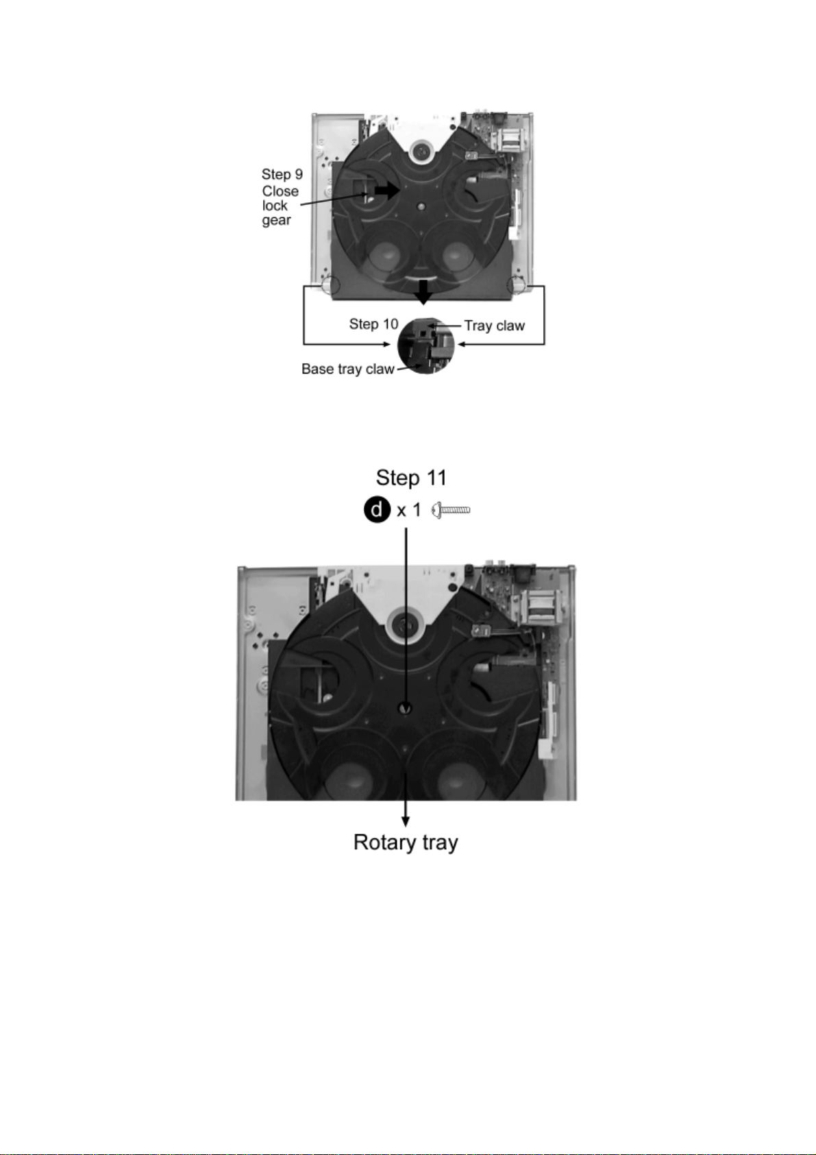
Step 9 Keep the close lock gear pressed in the direction shown, and move the tray in the direction shown.
Step 10 Fit the claw of the tray and the claw of the Base tray guide (left & right side).
Step 11 Remove the screw and the Rotary tray.
file:///E|/_MANUALS/TECHNICS/technics_sl-pd7nasvc_[ET]/NA/SL-PD7/SVC/s0801000000.html[30/09/2009 12:14:30]
Page 20
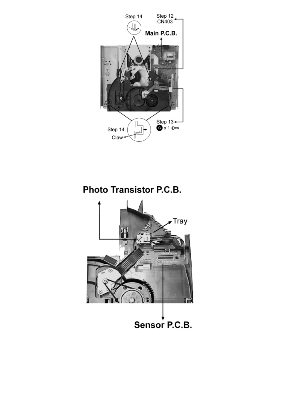
Step 12 Remove the connector CN403.
Step 13 Remove the screw.
Step 14 Pull the claw in the direction shown and remove the tray.
file:///E|/_MANUALS/TECHNICS/technics_sl-pd7nasvc_[ET]/NA/SL-PD7/SVC/s0801000000.html[30/09/2009 12:14:30]
Page 21
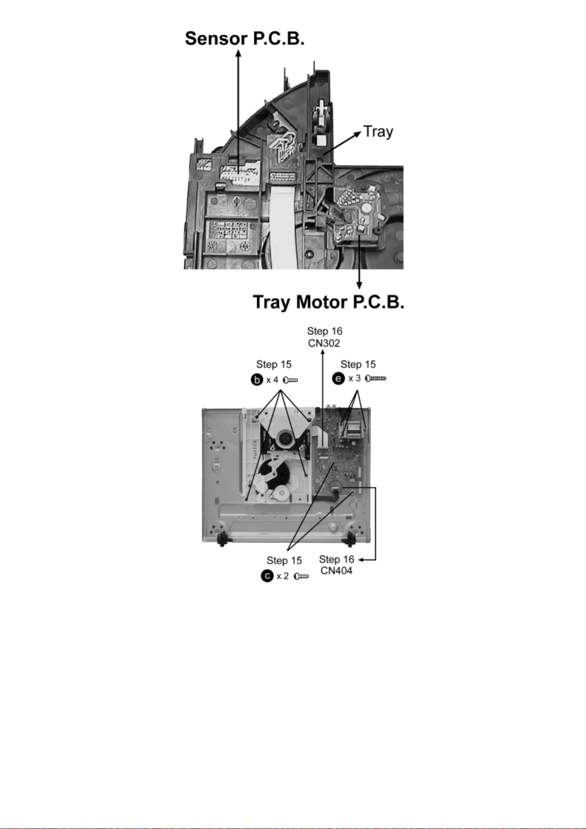
Step 15 Remove all the screws.
Step 16 Release the connectors CN302 and CN404.
file:///E|/_MANUALS/TECHNICS/technics_sl-pd7nasvc_[ET]/NA/SL-PD7/SVC/s0801000000.html[30/09/2009 12:14:30]
Page 22
TOP PREVIOUS NEXT
file:///E|/_MANUALS/TECHNICS/technics_sl-pd7nasvc_[ET]/NA/SL-PD7/SVC/s0801000000.html[30/09/2009 12:14:30]
Page 23
9 Self-Diagnostic Display Function
TOP PREVIOUS NEXT
Self-diagnostic display
This unit is equipped with a self-diagnostic display function which, if a problem occurs, will display an error code correcsponding to the problem.
Use this function when performing maintenance on the unit.
Entering the Self-Diagnostic Mode
1. With no CD loaded in the tray, turn on the unit.
2. Unplug the power cord of the unit, and then plug it back in while pressing the STOP (
), PLAY (
) and DISC 4 buttons together.This will bring up the FL display.
3. Release the above three buttons.
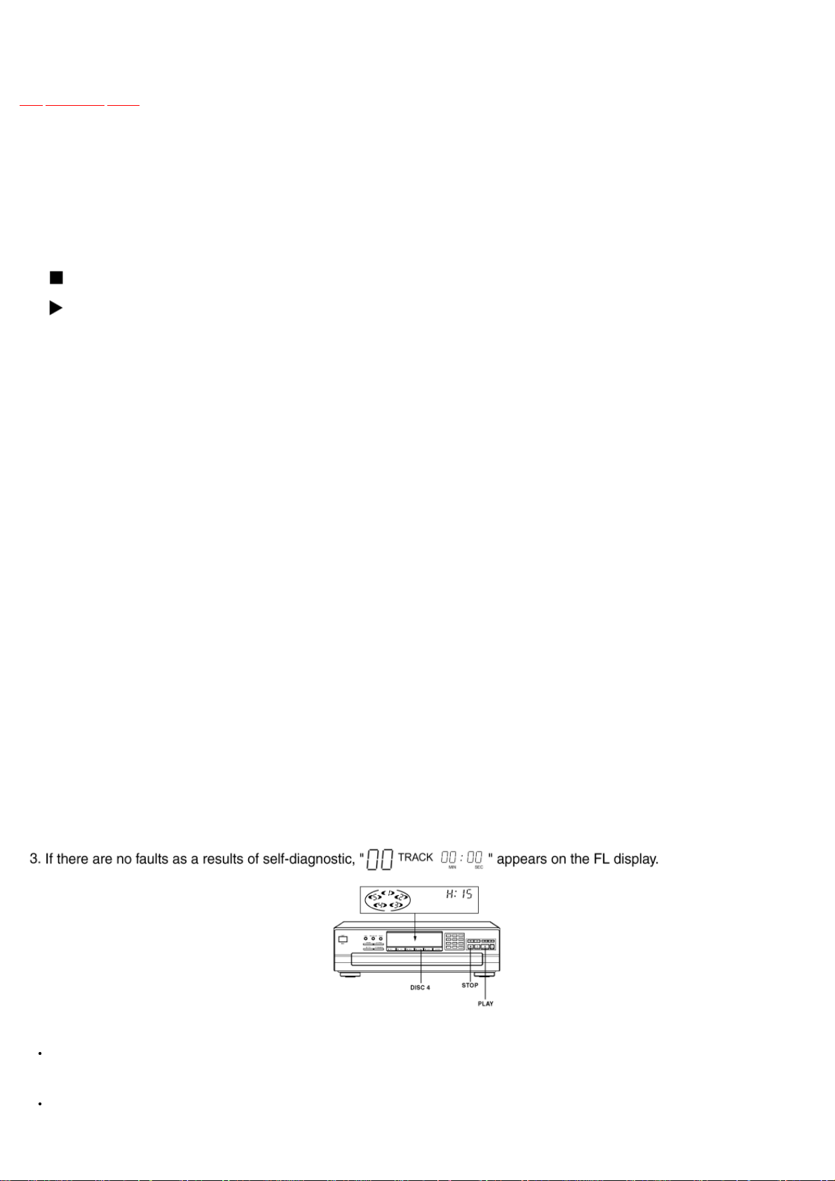
To Display Self-Diagnostics Results
1. When the FL display lights up, the unit automatically repeats an approximately 50-second cycle of the following operations.
START
A. Tray opens. -------- (A)
B. Tray closes. -------- (B)
C. Traverse deck lifts.
D. Tray opens.
E. Tray closes. -------- (B)
F. Traverse deck lower down.
G. Rotary tray turns counter-clockwise two disc slots. -------- (C)
H. Traverse deck lifts once, and then lowers
I. Rotary tray turns clockwise one disc slot. -------- (C)
J. Traverse deck lifts once, and then lowers
K. Rotary tray turns clockwise three disc slots. -------- (C)
L. Traverse deck lifts once, and then lowers
M. Rotary tray turns counter-clockwise one disc slot. -------- (C)
N. Traverse deck lifts once, and then lowers
O. Rotary tray turns counter-clockwise two disc slots./(Repeats from a - o).
2. Self-diagnostic fault results appear on the FL display for approximatelly one second as “H15” at location (A), “H16” at (B) and “H18” at (C), during the
above cycle.
To Return to Normal Display
Press the power button to off the unit, and then turn it on again.
To Display Self-Diagnostics Results Again
Follow steps 1 through 3 of “Entering Self-Diagnostic Mode” above.
file:///E|/_MANUALS/TECHNICS/technics_sl-pd7nasvc_[ET]/NA/SL-PD7/SVC/s0900000000x.html[30/09/2009 12:14:32]
Page 24

To Clear the Display of Self-Diagnostics Results
Turn off the unit to clear the contents of the stored faults results.
Interpretation of error codes
Error
code
H15 CD tray does not open or close when CD tray open/close(
H16
) button is pressed./When the CD open/close (
) button is pressed, the CD tray closes momentarily but then opens again, or opens momentarily and then
closes again.
F18 Faulty rotary turret rotation detection. Example : The turret continues to turn at the inintial position without
stopping.
Problem condition Correction procedure
TOP PREVIOUS NEXT
Faulty loading motor and motor drive IC (IC501), or faulty contact or short-circuit on open/close detect switch, S551. (Check
and replace)
Check the optical sensor (D501) and replace if necessary.
file:///E|/_MANUALS/TECHNICS/technics_sl-pd7nasvc_[ET]/NA/SL-PD7/SVC/s0900000000x.html[30/09/2009 12:14:32]
Page 25

10 Type Illustrations of ICs, Transistors& Diodes
TOP PREVIOUS NEXT
TOP PREVIOUS NEXT
file:///E|/_MANUALS/TECHNICS/technics_sl-pd7nasvc_[ET]/NA/SL-PD7/SVC/s1000000000x.html[30/09/2009 12:14:33]
Page 26

AN8885SBE1 (28p)
3
2
1
1
UPD78044F186 (80p)
MN662790RSC (80p)
1
BA4558FDXE2
8
1
4
BA6247N
5
1
10
BA033T
AN8739SBE2
2SD2037ETA
B
C
E
2SD1862QTV2
B
RSQGP1S53V
Ca
C
E
SG-206S
E
A
Ca
A
2SA1037AKSTX
C
B
E
KRC101MTA MTZJ3R6BTA
E
C
B
2SB1238QRTV2
2SD1859QRTV2
B
C
E
GL380
PT381
Anode
Cathode
A
Ca
2SD2144STA
B
C
E
RVD1SS133TA
A
Anode
Ca
Cathode
B
A
Anode
2SC2785FETA
KRA103MTA
KRC107MTA
C
E
Ca
Cathode
KRC111MTA
MTZJ30BTA
MTZJ5R1BTA
MTZJ5R6BTA
MTZJ6R2CTA
MTJZ6R8CTA
MTJZ9R1BTA
MTZJ9R1CTA
RL1N4003S-P
Ca
Cathode
C
C
E
A
Anode
Page 27

11 Terminal Functions of ICs
TOP PREVIOUS NEXT
11.1 IC701 (AN8885SBE1) Servo Amplifier
11.2 IC702 (MN662790RSC) Servo processor/ Digital signal processor/ Digital filter/ D/A converter
11.3 IC703 (AN8739SBE2) Focus coil/ Tracking coil/ Traverse motor/ Spindle motor driver
11.4 IC401 (C2BBGD000075) Microprocessor
TOP PREVIOUS NEXT
file:///E|/_MANUALS/TECHNICS/technics_sl-pd7nasvc_[ET]/NA/SL-PD7/SVC/s1100000000x.html[30/09/2009 12:14:33]
Page 28

11.1 IC701 (AN8885SBE1) Servo Amplifier
TOP PREVIOUS NEXT
Pin No. Mark I/O Function
1 PDE I Tracking signal input 1
2 PDF I Tracking signal input 2
3 VCC I Power supply
4 PDA I Focus signal input terminal 1
5 PDB I Focus signal input terminal 2
6 LPD I APC amp input
7 LD O APC amp output
8 RF O RFsumming output
9 RFIN I Detector’s input
10 CSBRT I Capacitor for OFTR connection
11 CEA I Capacitor for HPF amp connection
12 BDO O BDO output (“H” : drop out)
13 LDON I APC control
14 GND - Ground
15 /RFDET O NRFDET output (“L” : detection)
16 PDOWN O Power- down input
17 OFTR O OFTR output
18 NC O N.C.
19 ENV O 3T - ENV output
20 NC I N.C.
21 NC I N.C.
22 TEN I TE amp input
23 TEOUT O TE amp output
24 FEOUT O FE amp output
25 FEN I FE amp input
26 VREF O Reference voltage output
27 TBAL I Tracking balance control
28 FBAL I Focus balance control
TOP PREVIOUS NEXT
file:///E|/_MANUALS/TECHNICS/technics_sl-pd7nasvc_[ET]/NA/SL-PD7/SVC/s1101000000.html[30/09/2009 12:14:34]
Page 29

11.2 IC702 (MN662790RSC) Servo processor/ Digital
signal processor/ Digital filter/ D/A converter
TOP PREVIOUS NEXT
Pin
Mark I/O Function
No.
1 BCLK O N.C.
2 LRCK O N.C.
3 SRDATA O N.C.
4 DVDD1 I Power supply input (for digital circuit)
5 DVSS1 I GND (for digital circuit)
6 TX O Digital audio interface signal output (Latches data at first transition)
7 MCLK I Microprocessor command clock signal input
8 MDATA I Microprocessor command data signal input
9 MLD I Microprocessor command load signal input
10 SENSE O Sense signal output (OFT, FESL,MAGEND,NAJEND, POSAD,SFG) (Not used, open)
11 /FLOCK O Focus servo feeding signal output (“L” : Feed)
12 /TLOCK O Tracking servo feeding signal output (“L” : Feed)
13 BLKCK O Sub-code block clock signal output (BLKCKf = 75Hz during normal playback)
14 SQCK I External clock signal input for sub- code Q resistor
15 SUBQ O Sub- code Q code output
16 DMUTE I Muting input (“H” : mute)
17 STAT O Status signal output(CRC,CUE,CLVS,TTSTVP,/FCLV,SQCK)
18 /RST I Reset signal input
19 SMCK O 1/2- diveded clock signal of crystal osscillating at MSEL = “H” (fSMCK = 8.4672 MHz) 1/4 - divided clock signal of crystal oscillating at MSEL = “L”
20 CSEL I Frequency Selection Terminal H = 33.8688 MHz ; L = 16.9344 MHz
21 TRV O N.C
22 TVD O Traverse drive output
23 PC O Spindle motor ON output ("L" : ON)
24 ECM O Spindle motor drive signal output(forced mode output)
25 ECS O Spindle motor drive signal output(servo error signal output)
26 KICK O N.C.
27 TRD O Tracking drive output
28 FOD O Focus drive output
29 VREF I D/A (drive) output (TVD, ECS, TRD, FOD, FBAL, TBAL) Reference voltage input
30 FBAL O Focus balance adjustment output
31 TBAL O Tracking balance adjustment output
32 FE I Focus error signal input (analog input)
33 TE I Tracking error signal input (analog input)
34 RFENV I RF envelope signal input
35 VDET I Vibration detection signal input ("H" :detection)
36 OFT I Off- track signal input ("H" : off track)
37 TRCRS I Track cross signal input
38 /RFDET I RF detection signal input ("L" : detection)
39 BDO I Dropout signal input ("H" : Dropout)
40 LDON O Laser on signal output ("H" : ON)
41 PLLF2 I/O N.C.
42 DSLF2 O Tracking Offset alignment output/DSL Balance Output (DA Output)
43 WVEL O N.C.
44 ARF I RF signal input
(fSMCK = 4.2336MHz)
file:///E|/_MANUALS/TECHNICS/technics_sl-pd7nasvc_[ET]/NA/SL-PD7/SVC/s1102000000.html[30/09/2009 12:14:35]
Page 30

45 IREF I Reference current input
46 DRF I DSL bias terminal (Not used, open)
47 DSLF I/O DSL loop filter terminal
48 PLLF I/O PLL loop filter terminal
49 VCOF I/O VCO loop filter terminal
50 AVDD2 I Power supply input (for analog circuit)
51 AVSS2 I GND (for analog circuit)
52 EFM - EFM signal output
53 PCK - PLL extraction clock output (fPCK = 4.321 MHz during normal playback)
54 VCOF2 I/O VCO Loop filter for 33.8688 MHz conversation terminal for 16.9344 MHz crystal mode, must use other circuit
55 SUBC O Sub-code serial data output
56 SBCK I Clock input for sub- code serial data
57 VSS I GND
58 X1 IN I Crystal oscillating circuit input (f = 16.9344MHz)
59 X2 OUT O Crystal oscillating circuit input (f = 16.9344 MHz)
60 VDD I Power supply input (for oscillating circuit)
61 BYTCK - Byte clock output
62 /CLDCK - Sub - code frame clock signal output (fCLDCK = 7.35 kHz during normal playback)
63 FCLK - Crystal frame clock signal output (fCLK = 7.35 kHz, double = 14.7 kHz)
64 IPFLAG - Interpolation flag output (“H” : Interpolation)
65 FLAG - Flag output
66 CLVS - Spindle servo phase synchronizing signal output ("H" : CLV, "L" : rough servo)
67 CRC - Sub - code CRC checked output (“H’ :OK, “L” :NG)
68 DEMPH - De- emphassis ON signal output (“H” :ON)
69 RESY - Frame re - synchronizing signal output
70 IOSEL I Mode Switching Terminal
71 /TEST I Test input
72 AVDD1 I Power supply input (for analog circuit)
73 OUTL O Left channel audio signal output
74 AVSS1 I GND
75 OUTR O Right channel audio signal output
76 RSEL I RF signal polarity assignment input (at "H" level, RSEL="H", at "L" level, RESL="L")
77 IOVOD I 5V supply input
78 PSEL I Test terminal (connected to Gnd)
79 MSEL I SMCK oscillating frequency designation input (“L”:4.2336 MHz, “H”:8.4672 MHz)
80 SSEL I SUBQ output mode select (“H”:Q - code buffer mode)
TOP PREVIOUS NEXT
file:///E|/_MANUALS/TECHNICS/technics_sl-pd7nasvc_[ET]/NA/SL-PD7/SVC/s1102000000.html[30/09/2009 12:14:35]
Page 31

11.3 IC703 (AN8739SBE2) Focus coil/ Tracking coil/
Traverse motor/ Spindle motor driver
TOP PREVIOUS NEXT
Pin No. Mark I/O Function
1 /RST - RESET output terminal
2 NC - N.C.
3 IN2 I Motor Drive (2) input
4 PC2 I Turntable motor drive signal (“L :ON)
5 NC - N.C.
6 IN1 I Motor driver (1) input
7 NC I N.C.
8 PVCC1 I Power supply (1) for driver
9 PGND1 - Ground connection (1) for driver
10 NC - N.C.
11 D1- O Motor driver (1) reverse- action output
12 D1+ O Motor driver (1) forward-action output
13 D2- O Motor driver (2) reverse- action output
14 D2+ O Motor driver (2) forward-action output
15 D3- O Motor driver (3) reverse- action output
16 D3+ O Motor driver (3) forward-action output
17 D4- O Motor driver (4) reverse- action output
18 D4+ O Motor driver (4) forward-action output
19 NC - N.C.
20 PGND2 - Ground connection (2) for driver
21 PVCC2 I Power supply (2) for driver
22 NC - N.C.
23 VCC I Power supply terminal
24 VREF I Reference voltage input
25 IN4 I Motor driver (4) input
26 IN3 I Motor driver (3) input
27 RSTIN I Reset terminal
28 NC - N.C.
TOP PREVIOUS NEXT
file:///E|/_MANUALS/TECHNICS/technics_sl-pd7nasvc_[ET]/NA/SL-PD7/SVC/s1103000000.html[30/09/2009 12:14:37]
Page 32

11.4 IC401 (C2BBGD000075) Microprocessor
54 SYNCHRO - Not used, open
TOP PREVIOUS NEXT
Pin No. Mark I/O Function
1~7 G7~G1 O Grid signal of FL display
8 VDD - Power supply terminal
9 MCLK O Command clock signal
10 MDATA O Command data signal
11 MLD O Command load signal (“L” LOAD.)
12 SENSE I Sense signal
13 DMUTE O Muting control signal
14 SQCK O Sub-code Q register clock
15 NC - Not connected
16 SUBQ I Sub- code Q data
17 /RESET I Reset signal input
18 ZSENSE - Not used, connected to GND
19 REC.EN I Synchro. rec. control terminal
20 AVSS - GND terminal
21 /RSTSV O Reset signal output
22 OPEN I Open detect terminal
23 DIR O Motor control signal
24 TURN O Motor control signal
25 LOAD O Motor control signal
26 AD3 I Key input 3
27 AD2 I Key input 2
28 AD1 I Key input 1
29 AVDD I Power supply terminal
30 AVREF - Power supply terminal
31 NC - Not used, connected to GND
32 XT2 - Not used, open
33 VSS - GND Terminal
34 X1 I Crystal Osc. Input terminal (4.2336MHz)
35 X2 O Crystal Osc. Output terminal (4.2336MHz)
36 RESETSW O Rest position detect
37 UP/DOWN I Traverse deck up/down fetection input
38 Unused I Not used, connected to GND
39 Unused I Not used, connected to GND
40 Unused I Not used, connected to GND
41 Unused I Not used, connected to GND
42 Unused I Not used, connected to GND
43 PWM O Mechanism control signal (PWM output)
44 POFF I Power OFF detection input
45 POSITION I Rotary tray position detecting sensor input
46 SPEED I Loading motor speed sensor input
47 REMOCON I Remote control sensor input
48 IC - Not used, connected to GND
49 /TLOCK I Optical servo condition (tracking) input
50 /FLOCK I Optical servo condition (focus) input
51 STAT I Status signal (CRC,CUE,CLVS,TTSTOP, FCLV,SQCK)
52 VDD - Power supply terminal (+5V)
53 POWER O Power ON/OFF output terminal
file:///E|/_MANUALS/TECHNICS/technics_sl-pd7nasvc_[ET]/NA/SL-PD7/SVC/s1104000000.html[30/09/2009 12:14:38]
Page 33

55 DISC1 O DISC 1 LED control output
56 DISC2 O DISC 2 LED control output
57 DISC3 O DISC 3 LED control output
58 DISC4 O DISC 4 LED control output
59 DISC5 O DISC 5 LED control output
60 NC I Not used, connected to GND
61 S16 O Segment signal of FL display
62 S15 O Segment signal of FL display
63 S14 O Segment signal of FL display
64 S13 O Segment signal of FL display
65 S12 O Segment signal of FL display
66 S11 O Segment signal of FL display
67 S10 O Segment signal of FL display
68 S9 O Segment signal of FL display
69 S8 O Segment signal of FL display
70 S7 O Segment signal of FL display
71 VPP I Power supply terminal
72 S6 O Segment signal of FL display
73 S5 O Segment signal of FL display
74 S4 O Segment signal of FL display
75 S3 O Segment signal of FL display
76 S2 O Segment signal of FL display
77 S1 O Segment signal of FL display
78 NC I Not used, connected to GND
79 NC I Not used, connected to GND
80 G8 O Grid signal of FL display
TOP PREVIOUS NEXT
file:///E|/_MANUALS/TECHNICS/technics_sl-pd7nasvc_[ET]/NA/SL-PD7/SVC/s1104000000.html[30/09/2009 12:14:38]
Page 34

12 Block Diagram
TOP PREVIOUS NEXT
TOP PREVIOUS NEXT
file:///E|/_MANUALS/TECHNICS/technics_sl-pd7nasvc_[ET]/NA/SL-PD7/SVC/s1200000000x.html[30/09/2009 12:14:40]
Page 35

RF
TRAVERSE
MOTOR
SPINDLE
MOT
OPTICAL PICKUP
SEMICONDUCTOR
+B
PHOTO DETECTOR
EDE
DAC
F F
TRACKING
COIL
T+ T-
M
_
M
_
OR
LASER
POWER DRIVE
C
B
FOCUS
COIL
F-F+
IC703
AN8739SBE2
FOCUS COIL/
TRACKING COIL/
VERSE MOTOR/
TRA
SPINDLE MOTOR DRIVER
D4+
18
D4-
17
D3+
16
TRACKING
D3-
15
D1+
12
TRAVERSE
D1-
11
D2+
14
D2-
13
IC701
AN8885SBE1
SERVO AMP
6
LPD
Q701
LASER
+B
IC702
MN662790RSC
SERVO PROCESSOR/
DIGIT
PROCESSOR/
DIGITAL FILTER/
D/A CONVERTER
RESET
SIGNAL
GEN.
FOCUS
COIL
DRIVE
COIL
DRIVE
MOT
OR
DRIVE
SPINDLE
MOT
DRIVE
LDON
RF
AL SIGNAL
/RST
OR
7
LD
13
LDON
PDA
4
PDB
5
1
PDE
2
PDF
BDO
/RFDET
RFENV
FE
TE
OFT
VREF
TBAL
FBAL
LDON
1
26
IN3
IN4
25
IN1
6
IN2
3
PC2
4
+
-
+B
+B
ARF
44
39
BDO
/RF DET
38
RF ENV
34
FE
32
TE
33
OFT
36
TRCRS
37
VDET
35
VREF
29
TBAL
31
FBAL
30
PLLF2
41
WVEL
43
DSLF2
42
LDON
40
+B
+B
+
F
+
47 48
SYNCHRONIZING
PROTECTION
+B
+B
DSLF
DSL
SERVO
INPUT
POR
CONVER
TRD
28
+B
8
RF
RFIN
-
VCBA
+B
Ech
VCBA
Fch
TBAL
27
TBAL
ARATOR
RAM
ADDRESS
TOR
CLV
SER
VO
SERVO OUTPUT
POR
ECM
TRV23PC
24
Ach
Bch
PLLF
COMP
VCO
DEMODULA
TION
T
SENSE
10 11
+
FBAL
28
FBAL
FREQUENCY
ARATOR
EFM DATA
TOR
16K
SRAM
DETECT
AUTO CUE
SUB-CODE
DEMODULA
CHECK
CHECK
FLOCK
/RST
TLOCK
/RST
Subtracter
PEAK
CRCC
CRCC
OR/
TOR
Subtracter
+B
+B
TEIN
PDOWN
22 23
16
+B
SYNDROME
CALCULA
CIRC
DECODER
INTERPOLATION/
SOFT MUTING/
DIGITAL
ATTENUATION
BLKCK
SQCK
SUBQ
1418 1312 15
SQCK
SUBQ
+B
-
A
+
B
+
+B
+B
PHASE
COMP
SYNCHRONING
INTERPOLA
PROTECTION
T
A/D
GENERA
CONVERTER
SERVO
CPU
D/A
TER
TVD27FOD
KICK
ECS
22
25
2126
RF
.
DET
+
+
-
+B
TEOUT
TE
TION
109
CSBRT
OFTR
DET
BDO
.
DET
+B
21
CONVER
DIGITAL DE-EMPHASIS
DIGITAL FILTER
MASH LOGIC
.
+B
N.C.
S/P
TER
PWM
LOGIC
PWM
LOGIC
MICROMPUTER
INTERF
MDATA
STAT
8 7 9
17
MDATA
STAT
11
TENV
+
DIGITAL AUDIO
INTERF
ACE
MCLK
MCLK
+B
CEA
3
+
+
+
ACE
TIMING
GENERA
PITCH
CONTROL
MLD
MLD
TOR/
ENV
19
OFTR
17
BDO
12
/RFDET
15
FEN
25
FEOUT
24
VCC
3
26
VREF
GND
14
N.C.
18
TX
6
DMUTE
16
X2
59
X1
58
SMCK
19
RSEL
76
29
VREF
OUTL
+
-
73
OUTR
75
+
-
SUBC
55
SBCK
56
5
DVSS1
20
CSEL
78
PSEL
79
NSEL
/CLDCK
62
ENV
OFTR
BDO
/RFDET
FE
+B
+B
JK321
-B
X701
+B
+B
CD SIGNAL
RCH
Page 36

IC11
BA033T
REGULATOR
SIGNAL LINES
CD SIGNAL LINE
JK801
LCH OUT
STAT
Q801(Q802)
Q851,Q852
+B
S701(RESET)
Q475
SWITCH
MUTING
MUTING
IC801
BA4558FDXE2
L.P.F.
FILTER AMP
D801,D802
Q853
+B
MUTING
CD SIGNAL
+B
+B
Q18,Q19
POWER
SUPPL
CONTROL
D16
D42,D43
Y
REGULATOR
CURRENT
CONTROL
Q11,Q12
SWITCH
Q15
Q42
+B
TO FL DISPLAY
8
+B
6
4
5
D11~D14
D51,D52
-B
REGULATOR
IC501
BA6247N
MOTOR DRIVE
& AMP
CONTROL CIRCUIT
PT11
Q31
D21
MOTOR
DRIVE
MOTOR
DRIVE
MOTOR
DRIVE
D31,D32
Q32,Q33
FL DRIVE
M501
(LOADING MOTOR)
10
3
2
+
M
-
-
M
+
POWER TRANSFORMER
M551
(TRAY MOTOR)
JK11
AC INLET
SUBQ
SQCK
/RST
MCLK
MDATA
MLD
Q474
SWITCH
14
21
9
10
11
SQCK
/RST
MCLK
MDATA
MLD
16 51
SQCK
Q501
STAT
45
36
RESTSW
POSITION
D502,D551
UP/DOWN
SPEED
D501
13
+B
DMUTE
53
23
DIR
POWER
UPD78044F186
OPEN
2237,46
S551
Q462
MOTOR
CONTROL
25
24 43
LOAD
TURN
IC401
MICRO-PROCESSOR
G8
G1
S1
1~7,80
(OPEN/CLOSE DET.)
FL601
FL DISPLAY
61~70,72~77
D462
S16
Q461
MOTOR
CONTROL
PWM
KEYOUT1
26~28
KEY MATRIX
KEYOUT6
X401
3534
X1
X2
RESET
17
Q401
RESET
Page 37

13 Schematic Diagram
TOP PREVIOUS NEXT
(All schematic diagrams may be modified at any time with the development of new technology.)
Notes:
The voltage value and waveforms are the reference voltage of this unit measured by DC electronic voltmeter
(high impedance) and oscilloscope on the basis of chassis. Accordingly, there may arise some error in
voltage values and waveformsdepending upon the internal impedance of the tester or the measuring unit.
< > ...FM
( ) ...AM
Importance safety notice:
Components identifed by mark have special characteristics important for safety. Furthermore, special parts
which have purposes of fire-retardant (resistors), high-quality sound (capacitors), low-noise (resistors), etc.
are used. Whenreplacing any of components, be sure to use only manufacturer’s specified parts shown in the
parts list.
Caution!
IC, LSI and VLSI are sensitive to static electricity.
Secondary trouble can be prevented by taking care during repair.
Cover the parts boxes made of plastics with aluminium foil.
Put a conductive mat on the work table.
Ground the soldering iron.
Do not touch the pins of IC, LSI or VLSI with fingers directly.
TOP PREVIOUS NEXT
file:///E|/_MANUALS/TECHNICS/technics_sl-pd7nasvc_[ET]/NA/SL-PD7/SVC/s1300000000x.html[30/09/2009 12:14:40]
Page 38

SCHEMATIC DIAGRAM -1
: +B SIGNAL LINE
CD SERVO CIRCUIT
: CD SIGNAL LINE
OPTICAL PICKUP CIRCUIT
LASER DIODE
6
8
11
C
12
10
5
4
9
2
3
C
C
NBOUT
1
8
GND
GND
2
VCC
NAOUT
3
BIN
VREF
4
AIN
C
7
6
5
C
R701
4.7
3.2V
1
2
3
4
5
6
7
8
9
10
11
12
13
14
15
16
VCC
PDF
PDE
LD
LD GND
GND
NB
GND
NA
VREF
LPD
GND
TT+
FF+
Q701
R750
4.7
0.9V
((2V))
C713
C750
0.1
C751
0.1
0.1
CN701
1
2
3
4
5
6
7
8
9
10
11
12
13
14
15
16
C701
6.3V33
2.7V
((2.3V))
Q701
2SA1037AKSTX
LASER POWER DRIVE
C714
6.3V100
IC701
AN8885SBE1
SER
VO AMP
C712
C711
29
30
C703
6.3V100
C704
0.1
0.1
2700P
C707
C702
0.027
C706
1.6V
1.6V
1.6V
0V((0.2V))
3.2V
2.7V((2.3V))
1
1.6V
3
2
4
876
5
LD
LPD
PDB
PDF
PDA
VCC
PDE
IC701
TEN
TEOUT
FEOUT
TBAL
FEN
VREF
FBAL
24
23 2228
25
26
27
1.6V
1.6V
C747
180P
R744
120K
0.1
C749
2200P
0.1
R708
R707
22K
39K
21
1.6V
1.6V
1.6V
1.6V
1.6V
C710
120P
R702
R705
10K
150K
C742
0.027
R704
R706
1K
0.9V((1.4V))
9
RF
RFIN
NC
NC
20
1K
0V
0.7V
0V((3.1V))
1.6V
1.9V
14
1312
10
11
CEA
BDO
GND
LDON
CSBRT
NC
ENV
OFTR
PDOWN
/RFDET
17
15
19
16
18
0V
1.6V
0V((3.2V))
33
C735
0.1
C734
10V220
14 13 12 11 10
36
SP MOTOR
38
3.3V((3V))
3.3V((3V))
3.3V((3.5V))
D3-
D4-
D3+
D2+
D2-
D1+
3.3V
3.3V((3.5V))
3.7V((3.5V))
C737
0.1
M
M702
C736
0.1
M
M701
TRV MOTOR
3.3V
1915 16 17 18
D4+
NC
NC
D1-
3.7V((4.1V))
IC703
AN8739SBE2
FOCUS COIL/
TRACKING COIL/
VERSE MOTOR/
TRA
SPINDLE MOTOR DRIVE
7.3V
7.3V
29
2120
22 282726
23
GND
NC
GND
NC
7 6 5 4 3 2 1
30
VCC
IN1
PGND2
PGND1
9 8
PVCC2
IC703
PVCC1
35
1.6V
R735
100
1.6V
7.3V
1.6V
1.6V
25
24
VREF
NC
1.6V
IN4
PC2NCIN2
3.2V((0V))
NC
IN3
RSTIN
1.6V
R724
18K
1.6V
R725
390
R715
/RST
C715
2700P
1K
R727
3.9K
R736
100
C752
1000P
R749
4.7K
C738
0.01
R729
3.9K
C739
1500P
R728
3.9K
37
R723
6.8K
R731
6.8K
Page 39

X701
RSXB16M9J02T
C722
10P
R711
82K
C716
820P
SCHEMATIC DIAGRAM - 2
C754
470P
C723
C717
0.1
R714
120
C744
5600P
R709
47K
C721
10P
C718
0.22
10V220
C724
0.1
R712
220
R741
47K
R742
220K
626364 65
61
FCLK
60
VDD
BYTCK
3.2V
/CLDCK
59
X2
OUT
1.5V
58
IN
X1
1.5V
57
VSS
56
SBCK
55
SUBC
54
VCOF2
53
PCK
52
EFM
51
AVSS2
50
AVDD2
3.2V
49
VCOF
48
PLLF
0.5V
DSLF
47
1.6V
46
DRF
1.6V
45
IREF
1V
44
ARF
1.6V
43
WVEL
DSLF2
42
1.5V
PLLF2
41
/RFDET
BDO
LDON
40
39 38 37 36 35 34 33 32 31 30 29 28 27 26 25 24 23 22 21
0V
0V((3.2V))
0V((3.2V))
6667686970
CRC
CLVS
FLAG
IPFLAG
IC702
MN662790RSC
SERVO PROCESSOR
DIGIT
DIGITAL FILTER/
D/A CONVERTER
TRCRS
RFENV
VDET
OFT
0V
: +B SIGNAL LINE
R721
100
C731
6.3V220
C730
0.1
3.2V
2.9V
3.2V
73
71
72
RESY
/TEST
IOSEL
AVDD1
DEMPH
AL SIGNAL PROCESSOR/
VREF
FBAL
TBAL
TE
FE
1.6V
1.6V
1.6V
1.6V
1.6V
1.6V
OUTL
FOD
: CD SIGNAL LINE
20
18
13
23
R717
1K
R718
1K
C733
C732
0.1
6.3V220
3.2V
2.9V
1.5V
1.5V
74
76
75
RSEL
OUTR
AVSS1
TRD
KICK
1.6V
1.6V
3.2V
80
77
78
79
SSEL
PSEL
MSEL
1.6V
PC
3.2V((0V))
SRDATA
DVDD1
DVSS1
MDATA
SENSE
/FLOCK
/TLOCK
BLKCK
SQCK
SUBQ
DMUTE
SMCK
TVD
1.6V
BCLK
LRCK
MCLK
STAT
/RST
CSEL
1
2
3
4
3.2V
5
TX
6
1.6V
7
3.2V
8
0.5V
MLD
9
3.2V
10
11
12
13
0V
14
0V((0.2V))
15
3.2V((3.1V))
16
17
0V((3.1V))
18
3.1V
19
20
TRV
IOVDD
ECM
ECS
1.6V
C725
1000P
C726
1000P
C745
1000P
C727
50V1
C728
50V1
22
21
CN702
Lch OUT
19
A.GND
18
Rch OUT
17
11
10
9
C753
470P
C743
0.1
8
6
7
4
R753
10
3
+3.3V
D.GND
LD SW
+7.5V
P.GND
MCLK
MDATA
MLD
SPEED
BLKCK
SQCK
SUBQ
STAT
/RST
REST SW
17
16
15
14
TX
13
TO
12
MAIN
11
CIRCUIT
10
(CN302) ON
9
SCHEMA
8
7
6
5
4
3
2
1
TIC
DIAGRAM-3
2
TJ
TJ701
S701
REST SW
16
1
15
Page 40

SCHEMATIC DIAGRAM-3
TO
LOADING
OR
MOT
CIRCUIT
(CN551) ON
SCHEMATIC
DIAGRAM-6
TO
SENSOR
CIRCUIT
(CN501) ON
TIC
SCHEMA
DIAGRAM-6
TO
VO
CD SER
CIRCUIT
(CN702) ON
SCHEMATIC
DIAGRAM-2
CN404
CN403
CN302
MAIN CIRCUIT
LH+
6
5
4
3
2
1
14
13
12
11
10
9
8
7
6
5
4
3
2
1
19
18
17
16
15
14
13
12
11
10
9
8
7
6
5
4
3
2
1
LH-
LED
UP/DOWN
DGND
OPEN
P.GND
LH+
LHLOAD
TURN
DIREC
+8.5V
VREF
P.GND
+8.5V
LED
SPEED
POSITION
D.GND
OUTL
AGND
OUTR
3.3V
DGND
LD SW
TX
PVCC (8.0v)
PGND
MCLK
MDATA
MLD
SPEED
BLKCK
SQCK
SUBQ
STAT
/RST
REST_SW
G8
S1
S2
S3
S4
S5
S6
S7
S8
S9
S10
S11
S12
C462
0.01
R462
C301
((0.6V))
R431
((0.7V))
R435
10K
G1
2
1
3
R463
120
R461
220
0.01
10K
Q475
4.7K
R406
4
5
((2.5V))
6
120
((0V))
Q474
Q474, 475
KRC101MTA
SWITCHING
((0V))
R432
4.7K
R433
4.7K
R434
4.7k
((0V))
((-25.06V))
80
((0V))
79
((0V))
78
((-20.44V))
77
((-9.50V))
76
((-9.50V))
75
((-24.13V))
74
((-27.86V))
73
((-24.42V))
72
((-28.02V))
71
((-24.08V))
70
((-13.08V))
69
((-24.08V))
68
((-13.08V))
67
((-16.74V))
66
((-24.09V))
65
4.7K
R407
R447
4.7K
R442 4.7K
4.7K
R443
R444
R445
S3
S4
S1
S2
G8G7G6G5G4G3G2
897
TO
PANEL CIRCUIT
(CN601) ON
SCHEMATIC DIAGRAM-5
D461
((3.64V))
R436
1K
G7
G8
NC
NC
S1
S2
S3
S4
S5
S6
VPP
S7
S8
S9
S10
S11
S12
S13
4.7K
4.7K
S5
64
1413121110
D462
C314
0.01
R429
REST_SW
((-27.43V))
((-27.60V))
2
1
63
((-24.09V))
((-24.30V))
S6
S7S8S9
15
Q461, 462
KRC111MTA
MOTOR CONTROL
((6.83V))
((0V))
Q462
10K
((0V))
((0V))
R427
10K
10K
R430
4.7K
7
13
15
STAT
14
((-24.98V))
((-24.96V))
((-24.96V))
((-24.97V))
((-25.03V))
3
54
G1
G4
G3
G2
G5
G6
S14
S16
S15
DISC5
NC
DISC4
61
62
((0V))
((0V))
((-24V))
((4.99V))
((-23.50V))
4.7K
R440
S11
S12
S10
1918
1716
: +B Signal Line
C461
Q461
10K
((5.03V))
VDD
((0V))
R425
10K
R428
4.7K
((3.94V))
((3.56V))
9876
10
MCLK
((4.89V))
11
MDATA
MLD
R423
((0V))
10K
SENSE
((0V))
10V 47
10
((4.97V))
141312
SQCK
DMUTE
IC401
IC401
UPD78044F186
MICRO-P
STAT
SYNCHRO
VDD
DISC1
DISC2
POWER
DISC3
54
53
52
555657585960
51
((0V))
((0V))
((0V))
((0V))
S13
2120
C406
50V 1
CN401
((5.05V))
((4.98V))
0.01
C405
((2.60V))
STAT
R437
R438 10K
R439 10K
R420
10K
R424
R426
4.7K
((2.50V))
((5.03V))
((0.10V))
((0V))
((5V))
17
1615
NC
SUBQ
/RESET
REC.EN
ZSENSE
PWM
/FLOCKICSPEED
/TLOCK
REMOCON
50
((5V))
((0V))
((0V))
((0V))
((0.13V))
10K
CN402
: -B Signal Line
R422
MCLK
4.7K
4.7K
((0V))
((5V))
201918
AVSS
*
POSITION
((2.80V))
((0.80V))
C421
11
MDATA
MLD
SQCK
SUBQ
((0V))
((5V))
((0V))
2221
24
23
TURN
((0V))
DIR
25
LOAD
OPEN
((5.02V))
26
AD3
/RSTSV
((5.02V))
AD2
27
((5.02V))
AD1
28
((5.02V))
AVDD
29
((5.02V))
30
AVREF
((0V))
NC
31
((5.02V))
XT2
32
((0V))
33
VSS
((2.20V))
34
X1
((2.30V))
35
X2
((5.03V))
REST_SW
36
((5.03V))
37
UP/DOWN
((0V))
38
EE_CS
((0V))
39
EE_CLK
((0V))
EE_DATA
40
NC
NC
POFF
41
4243444546474849
((0V))
((0V))
((0V))
C423
10K
1000P
R421
1000P
+5V
S14
S16
AD3
AD2
GND
AD1
S15
8
4
7 5
9
6
10
TO
PANEL CIRCUIT
(CN602) ON
SCHEMATIC DIAGRAM-5
3
C424
1000P
: CD Signal line
R412 22K
R411 4.7K
10K
1.8K
R410
R409
Q401
2SC2785FETA
RESET
REST_
SW
470
Q401
0.01
R418
C402
100K
((0V))
6.3V 470
C408
C409
R414
C404
R415
100P
0.01
25V 4.7
56K
R416
22K
R417
47K
22K
R419
10k
R413
((5.05V))
C403
50V 1
((0V))
C401
J133
out
GND
in
X401
4.23MHz
4.7K
R402
4.7K
R401
R446
4.7K
C422
1000P
E400
SNE1004-2
C410
C407
0.1
0.1
FL1
FL2
2
1
Page 41

SCHEMATIC DIAGRAM-4
3
D23, 24
MTZJ9R1BTA
Z301
2
((8.62V))
D17
C17
6.3V 100
MTZJ3R6BTA
8
D54
RVD1SS133TA
4
D23
D24
5
9
((-18.85V))
Q32, 33
2SD2144STA
FL DRIVE
RL1N4003S-P
BA033T
REGULATOR
R21
560
RVD1SS133TA
Q32
Q33
3
IC11
D16
IC11
2
((0.02V))
D53
MTZJ5R1BTA
D46
R22
560
6
: +B Signal Line
C801
10V 47
C802
10V 47
1
4.7
R13
1
((3.26V))
D43
RL1N4003S-P
D42
RL1N4003S-P
C42
6.3V 100u
D44
((15.16V))
RVD1SS133TA
((15.24V))
Q12
2SB1238QRTV2
SWITCHING
D47
RVD1SS133TA
R32
((-18.17V))
10K
((-18.84V))
R33
((-18.16V))
10K
C803
16V 10
C804
16V 10
Q15
2SD2037ETA
REGULATOR
Q15
((9.63V))
((8.61V))
((9.27V))
C16
10V 470
D15
MTZJ9R1CTA
Q42
2SD1862QTV2
CURRENT CONTROL
Q42
R42
1
((8.61V))
((6.32V))
D41
MTZJ6R2CTA
Q11
KRC107MTA
SWITCHING
R43
22K
R44
10K
((14.52V))
Q12
((0V))
1000P
((-36.7V))
Q31
((-28.08V))
Q31
2SB1238QRTV2
D34
REGULATOR
MTZJ9R1CTA
R803
R804
C15
((9.67V))
((0V))
10K
47K
C33
((-28.66V))
220K
220K
1000P
R11
180
C43
Q11
1000P
((5V))
R805
8.2k
R806
8.2K
R12
180
((0V))
R41
470
: -B Signal Line
R807
12k
C815
82P
C816
82P
R808
12K
22K
22K
Q853
D21
RL1N4003S-P
C21
35V 100
C22
D22
25V 100
D31
C32
D32
50V 47P
RL1N4003S-P
12K
R31
R34
100
C807
560P
C808
560P
((5V))
C12
C31
C805
((5V))
390P
C806
390P
R852
1K
16V 3300
50V 47
: CD Signal line
JK321
DGND
1 2
1000P
1000P
0.01
1
+5.0V
2
TX
3
JK801
Lch
Rch
0.01
C30
JK11
AC IN
120V
2
60HZ
C322
R819
R820
PT11
C321
0.01
10
47K
C811
R817
47k
R818
C812
10
C11
CN14
5
4
CN11
1
1
6.3V 100
Q801, 802
2SD2144STA
IC801
((8.93V))
((0.01V))
5
8
((0.03V))
7
((0.01V))
6
R811
68K
R809
R810
((5V))
33K
33K
((0.01V))
((0.01V))
IC801
Q852
22K
R812
22K
((0V))
68K
2
1
((0.03V))
4
3
((-8.83V))
((0V))
22K
22k
Q851
D18
RL1N4003S-P
((0V))
11
12
BA4558FDXE2
5.6K
R851
((0V))
((0V))
C20
((0V))
Q18
((5V))
D33
MTZJ30BTA
Q19
R19
220
MUTING
R813
C809
1k
6.3V 47
D801
R815
((0V))
4.7K
D802
((0V))
R816
4.7K
((0V))
C810
R814
1K
6.3V 47
IC801
L.P. FILTER AMP
Q851, 852, 853
KRA103MTA
MUTING
D12
D14
D51, 52
RL1N4003S-P
R51
5.6K
R52
5.6K
CN21
1
1
CN20
1
CN19
1
CN18
1
CN17
50V 0.01u
CN16
1
Q18
2SD1859QRTV2
POWER SUPPLY CONTROL
((0.73V))
Q19
KRC107MTA
POWER SUPPLY CONTROL
((0.86V))
((0V))
Q801
((0V))
Q802
D11, 12, 13, 14
RL1N4003S-P
D11
D13
D51
D52
RTP1K4C030-X
2
11
2
10
9
2
8
2
7
6
2
2
Page 42

SCHEMATIC DIAGRAM-5
PANEL CIRCUIT
5
21
6
:+B Signal Line
FL601
RSL0274-F
1312
1514
11
9
10
87
181716
22
21
20
19
2625
2423
30292827
31
35
34
CN601
S13
1
S12
2
S11
3
S10
4
S9
5
S8
6
S7
7
S6
8
S5
9
TO
S4
10
12
13
14
15
16
17
18
19
20
11
21
S3
S2
S1
G8
G7
G6
G5
G4
G3
G2
G1
MAIN CIRCUIT
(CN401) ON
SCHEMATIC
DIAGRAM-3
R660
68K
S612
STOP
R671
68K
S624
REV SRCH
R680
10K
S634
EDIT GUIDE
R659
22K
0
S611
R670
22K
S623
FWD SRCH
R679
6.8K
S633
ID SCAN
R658
10K
10
S610
R669
10K
S622
REV SKIP
R678
4.7K
S632
TIME MODE
R657
6.8K
9
S609
R668
6.8K
S621
FWD SKIP
R677
2.7K
S631
PROGRAM
R656
4.7K
8
S608
R667
4.7K
S620
OPEN/CLOSE
R676
2.2K
S630
DISC1
R655
2.7K
S607
R666
2.7K
S619
R675
1.8K
S629
7
PLAY
DISC2
R654
2.2K
S606
R665
2.2K
S618
R674
S628
6
PAUSE
1.2K
DISC3
R652
R653
1.8K
1.2K
5
S604
S605
R663
R664
1.2K
1.8K
>10
S616
S617
R6731KR672
S626
S627
DISC4
4
REPEAT
1K
DISC5
R6511KR650
3
S603
R662
1K
S615
RANDOM
S625
DISC SKIP
1K
S602
R661
1K
S614
2
SPIRAL
S601
CN602
FL2
1
FL1
2
STBY
3
+5V
4
TO
GND
5
MAIN CIRCUIT
AD3
(CN402) ON
6
AD2
SCHEMA
DIAGRAM-3
TIC
7
AD1
8
S14
9
S15
10
S16
11
1
POWER
SWITCH
FC601
1
2
NC
3
CIRCUIT
S613
POWER
AD2
POWER
NC
AD3
1
2
3
FC601
Page 43

SCHEMATIC DIAGRAM-6
: +B Signal line
TRAYMOTOR
CIRCUIT
M
M501
D502
RSQGP1S53V
Q501
PT381
PHOTO
TRANSIST
CIRCUIT
SENSOR CIRCUIT
IC501
BA6247N
MOTOR DRIVE
Direction Select Amp Drive
6
9
8
10
0.5V
6
5
4
3
2
1
FC502
NC
3
2
1
FC503
6
5
4
3
2
1
FC502
3
2
1
FC503
8.6V
6.8V
7
5
0V0V0V
D501 GL380
IC501
1
2
3
4
0.5V
0.5V
P.GND
14
LH+
13
LH-
12
LOAD
11
TURN
10
DIREC
9
8
7
NC
6
+8.5V
5
4
3
2
1
CN501
+8.5V
VREF
P.GND
LED
SPEED
POSITION
D.GND
TO
MAIN CIRCUIT
(CN403) on
SCHEMATIC
DIAGRAM-3
OR
LOADING MOTOR
CIRCUIT
M551
M
D551
SG-206S
S551
SWITCH
6
5
4
3
2
1
CN551
LH+
LHLED
UP/DOWN
DGND
OPEN
TO
MAIN CIRCUIT
(CN404) on
SCHEMATIC
DIAGRAM-3
Page 44

14 Printed Circuit Board
TOP PREVIOUS NEXT
TOP PREVIOUS NEXT
file:///E|/_MANUALS/TECHNICS/technics_sl-pd7nasvc_[ET]/NA/SL-PD7/SVC/s1400000000x.html[30/09/2009 12:14:41]
Page 45

ABCDEFG
1
CD SERVO P.C.B (REPX0192E)
(RF)
TP20
C726
R718
80
TP11
TP7
TP6
TP3
J731
R717
1
C733
TP17
TP9
C728
TP25
TP26
C727
TP27
R753
J734
TP24
C745
TP1
C753
CN702
19
17
15
13
11
9
7
5
3
1
TP23
TP22
18
16
14
12
10
8
6
4
2
TP21
C725
C730
C754
C743
TP5
TP4
TP2
C731
R721
J716
C732
J715
TP10
TP8
TP12
2
TP19
TP18
3
4
5
X701
R714
C721
C744
C722
C724
60
61
IC702
20
21
J732
TP36
M702
SPL MOTOR
C717
C723
R731
R723
J721
S701
REST.SW
C738
M
R711
R741
41
40
R735
C703
R709
R712
R742
C718
TP42
C742
TP33
R724
R725
J724
R715
C715
C752
C704
C716
J701
28
C707
R705
R704
R749
R727
C706
14
15
C749
R728
R729
TJ701
TP29
C702
IC701
R702
C710
C747
R744
R706
R707
J728
C739
R736
28
R708
14
C714
1
C711
12
1516
J709
C712
C713
R750
11
13
15
J722
J710
J750
4
56
78
910
R701
J727
J702
J712
12
3
Q701
C750
C701
CN701
C
B
C751
E
(VREF)
6
TP37
M
M701
TRV MOTOR
C736
J704
TP16
TP15
TP38
C737
J707
J708
TP35
IC703
1
14
C735
C734
7
8
9
Page 46

D
R
J
9
J122
1
P
ABCDEFG
1
2
3
4
5
6
MAIN P.C.B. (REPX0249D)
TP11
C321
1
2
3
JK321
D801
R815
2
3
1
C811
JK801
JK11
J121
J120
J118
J114
R817
R818
Q802
B
C
R820
E
R819
Q801
B
C
E
C812
AC IN
120V 60HZ
OUT
OPTICAL
LINE
OUT
TP12
TP2
R816
C322
C809
R813
R814
J211
C810
D802
J301
J321
R811
X
C815
C807
R809
C801
R810
C808
C816
IC801
C806
C805
R807
58
R805
R803
4
1
R804
R812
R808
X
R806
PT11 (POWER TRANSFORMER)
PRIMARY
CN11
CN14
TP4
C803
C804
J220
J145
J601
J143
X
J312
C802
J131
SECONDARY
CN17
CN19
CN18
CN20
C30
CN16
J700
Q15
J503
D15
CN21
TP1
J504
J406
J405
J403
C15
C20
C11
B
X
J113
J505
R11
D17
C17
J308
Z301
C
C16
X
J407
D13
E
J119
TP3
X
X
IC11
C314
J136
D14
Q475
J134
J210
D16
3
2
1
C12
J169
C301
B
C
E
D11
J147
R851
TP5
J408
R13
D12
R435
C21
C22
C32
J112
J106
R41
D52
D51
CN302
18
16
14
12
10
8
6
4
2
R427
B
C
Q851
E
J310
J302
J102
J101
19
17
15
13
11
9
7
5
3
1
Q852
C31
Q18
D41
B
C
E
B
C
E
R852
D21
D22
J205
J149
R431
D31
C43
R42
R52
R51
R434
B
C
E
D32
Q42
J154
B
C
Q474
E
R429
J602
J204
D18
B
C
E
R463
C461
R461
D461
C
EB
J144
R428
J142
J218
J216
R432
Q853
J124
D23
D46
R12
D44
J116
R19
C33
J202
D53
D54
R433
J132
E
R43
D42
D43
R21
C
R44
Q11
B
C
E
C42
Q33
R420
R423
R425
14
13
12
11
10
9
8
Q461
7
6
5
4
3
2
1
CN403
J212
J223
X
B
Q12
D47
C
EB
Q1
C
EB
D33
R34
R31
Q31
J105
J600
B
C
R32
E
TP
J31
J137
R33
J400
T
7
CAUTION
RISK OF ELECTRIC SHOCK
AC VOLTAGE LINE. PLEASE DO NOT
TOUCH THIS P.C.B
8
9
Page 47

HG
5
B
IJKLM
J214
J309
J203
B
C
E
J221
J314
J215
R462
J107
J222
J315
J108
Q32
X
J316
J139
C404
R409
R410
J123
J401
J109
TP7
R415
R414
J156
J300
X
C423
J200
R430
D462
R413
C422
J305
R422
R424
R426
J306
D34
CN402
Q401
X
X
X
C
EB
C403
J129
J208
R419
R416
R402
R401
C408
C409
R417
J307
C421
J111
R437
J201
1
5
2346
TP10
J154
C461
J149
D461
B
C
Q474
E
R431
R429
R434
2
B
C
Q853
E
R852
D21
J124
D22
D31
D32
J602
R12
J205
J116
J204
D18
8
J202
B
C
C43
E
Q42
R42
D53
R52
R51
R463
R461
C
EB
J144
R428
J142
J218
J216
R433
R432
J132
R21
D23
D46
E
R43
D44
R19
C33
D42
D54
D43
R420
R423
R425
Q461
J212
X
C
B
R44
EB
EB
Q11
B
C
E
C42
B
C
E
Q33
13
11
9
7
5
3
1
CN403
J223
D47
C
C
D33
R34
R31
Q31
J600
14
12
10
8
6
4
2
Q12
Q19
R32
J311
J105
J137
D24
R22
R33
J209
J122
J400
J501
R418
7
R421
R446
X
8
J141
R436
9
10
J135
J125
J304
J104
111213
J126
Q462
J206
J115
R443
15
14 16
TP14TP15TP13
R412
B
C
E
C401
C405
J506
C402
R447
17
J313
X401
R444
J133
40
41
R442
R445
J127
321
J217
J800
C406
J100
C410
R438
R439
25
J140
J138
C424
IC401
64
J500
J110
R440
J404
J402
J502
J213
CN404
1
C407
2
3
C462
J303
4
5
6
J207
1
80
R407
65
15
R406
E400
CN401
9111213
5
1
7
6
14161718
234
10
8
24
1921
20
TP8
TP9
TP6
Page 48

ABCDEFG
C
R
2
1
1
2
3
PANEL P.C.B. (REPX0248D)
CN602
15
9111213
1
5
10
J616
3467
8
S624
REV SEARCH
R665
S612
STOPPAUSE
2
S621
FWD SKIP
S620
REV SKIP
R669
R668
PLAYOP/CLOSE
S622
S619
R667
17
1416
J615
J614
S623
FWD SEARCH
R671R670
R666
S618
J620
J621
S606
S609
S617
FL601
5
1
R652
S605
R660
S602
2
5
0
S611
R651
R654R655
S608
R657
S601
1
R650
S604
4
R653
S607
8
10
R659
7
R656R658
S610
S603
3
6
9
>10
J612
J613
J601
S625
DISC
SKIP
R672
S626
DISC 5
J622
J623
J624
10
2
4
POWER SWITCH P.C.B. (REPX0248D)
5
FC601
3
2
1
S613
POWER
6
PHOTO TRANSISTOR
P.C.B. (REPX0096A-N)
1
2
3
Q501
FC503
7
D501
5
4
3
2
CN501
1
2
1
FC502
3
11
13
5
79
101214
4
668
8
SENSOR P.C.B.
(REPX0096A-N)
FC503
321
IC501
110 2
3
456789
J501
9
Page 49

GHI J KL M
J601
FL601
1
S625
R672 R673
DISC
SKIP
5
S626
DISC 5
J622
J623
J624
CN601
1921
20
15
15
14161718
DISC 4
S627
20
789111213
6
10
10
25 30
1
5
3
2
4
S628
R674
DISC 3 DISC 2
R675
J610
35
J611
S629
TRAY MOTOR P.C.B. (REPX0096A-N)
6
5
4
3
2
1
FC502
M501
R676
S630
DISC 1
S634
R664
R663
S615
ID SCAN
R662
S632
TIME MD
R679R680
S633
S614
R661
S616
REPEAT RANDOM MODE SPIRAL
EDIT
GUIDE
S631
R677
PROGRAM
3
2
1
FC601
R678
D502
LOADING MOTOR P.C.B. (REPX0095A-N)
6
5
4
3
2
1
CN551
D551
S551
M551
Page 50

15 Troubleshooting Guide
TOP PREVIOUS NEXT
TOP PREVIOUS NEXT
file:///E|/_MANUALS/TECHNICS/technics_sl-pd7nasvc_[ET]/NA/SL-PD7/SVC/s1500000000x.html[30/09/2009 12:14:42]
Page 51

16 Wiring Connection Diagram
TOP PREVIOUS NEXT
TOP PREVIOUS NEXT
file:///E|/_MANUALS/TECHNICS/technics_sl-pd7nasvc_[ET]/NA/SL-PD7/SVC/s1600000000x.html[30/09/2009 12:14:42]
Page 52

17 Parts Location and Replacement Parts List
TOP PREVIOUS NEXT
Notes:
Important safety notice:
Components identified by mark have special characteristics important for safety.
Furthermore, special parts which have purposes of fire-retardant (resistors), high-quality sound (capacitors),
low-noise (resistors), etc. are used.
When replacing any of these components, be sure to use only manufacturers’s specified parts shown in the
parts list.
The parenthesized indications in the Remarks column specify the areas or color. (Refer to the cover page for
area or color.)
Parts without these indications can be used for all areas.
Capacitor values are in microfarad (µF) unless specified otherwise, P=Pico-farads(pF); Farads.
Resistance values are in ohms, unless specified otherwise, 1K=1,000(ohms).
The marking (RTL) indicates that the Retention Time is limited for this item. After the discontinuation of this
assembly in production, the item will continue to be available for a specific period of time. The retention
period of availabilityis dependant on the type of assembly, and in accordance with the laws govening part
and product retention. After the end of this period, the assembly will no longer be available.
[M] indicates in the Remarks columns indicates parts that are supplied by MESA .
The “(SF)” mark denotes the standard part.
Reference for O/I book languages are as follows :
Ar : Arabic Cf : Canadian French Cz : Czech Da : Danish
Du : Dutch En : English Fr : French Ge : German
It : Italian Ko : Korean Po : Polish Ru : Russian
Sp : Spanish Sw : Swedish Co : Traditional Chinese Cn : Simplified Chinese
17.1 CD Loading Mechanism
17.1.1 CD Loading Mechanism Part Location
17.1.2 CD Loading Mechanism Part List
17.2 Cabinet
17.2.1 Cabinet Parts Location
17.2.2 Cabinet Parts List
17.3 Electrical Parts List
17.4 Packing Materials& Accessories Parts List
17.5 Packaging
file:///E|/_MANUALS/TECHNICS/technics_sl-pd7nasvc_[ET]/NA/SL-PD7/SVC/s1700000000x.html[30/09/2009 12:14:43]
Page 53

TOP PREVIOUS NEXT
file:///E|/_MANUALS/TECHNICS/technics_sl-pd7nasvc_[ET]/NA/SL-PD7/SVC/s1700000000x.html[30/09/2009 12:14:43]
Page 54

17.1 CD Loading Mechanism
TOP PREVIOUS NEXT
17.1.1 CD Loading Mechanism Part Location
17.1.2 CD Loading Mechanism Part List
TOP PREVIOUS NEXT
file:///E|/_MANUALS/TECHNICS/technics_sl-pd7nasvc_[ET]/NA/SL-PD7/SVC/s1701000000.html[30/09/2009 12:14:44]
Page 55

17.1.1 CD Loading Mechanism Part Location
TOP PREVIOUS NEXT
TOP PREVIOUS NEXT
file:///E|/_MANUALS/TECHNICS/technics_sl-pd7nasvc_[ET]/NA/SL-PD7/SVC/s1701010000.html[30/09/2009 12:14:44]
Page 56

file:///E|/_MANUALS/TECHNICS/technics_sl-pd7nasvc_[ET]/NA/SL-PD7/SVC/loading.jpg[30/09/2009 12:56:30]
Page 57

17.1.2 CD Loading Mechanism Part List
TOP PREVIOUS NEXT
Ref. No. Part No. Part Name & Description Remarks
TRAVERSE DECK
301 RDG0270 SPEED REDUCTION GEAR [M]
302 RDG0271 DRIVE GEAR A [M]
303 RDG0272 DRIVE GEAR B [M]
304 RDK0025 DRIVE CAM [M]
305 RDP0050 PULLEY GEAR [M]
306 RFKPLPD667PB LOADING MOTOR ASS’Y [M]
307 RHD26019 SCREW [M]
308 RMG0268-K BELT [M]
309 RML0334 CHANGE LEVER [M]
310 RMM0117 SLIDE PLATE 1 [M]
311 RMM0118-1 SLIDE PLATE 2 [M]
312 RMR0746-W STRENGTHENING PLATE [M]
313 RFKNDCV51CAK MECHA BASE ASS’Y [M]
314 RMX0094 TRAY GUIDE [M]
315 RXQ0346-1 SLIDER ASS’Y [M]
316 XTB3+10JFZ SCREW [M]
358 RAE0152Z-3 TRAVERSE [M]
358-1 SHGD113-1 FLOATING CUSHION [M]
358-10 XQS17+A35FZ TRAVERSE MOTOR SCREW [M]
358-2 SNSD38 TRAVERSE MOTOR ASS’Y [M]
358-3 RAF0150A-4S 50A OPU [M]
358-4 RDG0247 DRIVE GEAR [M]
358-5 RDG0248 RELAY GEAR [M]
358-6 RXQ0339 TRAVERSE MOTOR ASS’Y [M]
358-7 RXQ0304-1 NUT PLATE ASS’Y [M]
358-8 XQN17+CG5 NUT PLATE ASSY SCREW [M]
358-9 XQS2+A3FZ SPINDLE MOTOR SCREW [M]
359 RME0142 FLOATING SPRING A [M]
360 RME0109 FLOATING SPRING B [M]
361 RMR0698-K1 TRAVERSE CHASSIS [M]
362 RMS0123-1 FIXED PIN B [M]
363 XTN2+6G SCREW [M]
364 RMS0350 FIXED PIN A [M]
TOP PREVIOUS NEXT
file:///E|/_MANUALS/TECHNICS/technics_sl-pd7nasvc_[ET]/NA/SL-PD7/SVC/s1701020000.html[30/09/2009 12:14:45]
Page 58

17.2 Cabinet
TOP PREVIOUS NEXT
17.2.1 Cabinet Parts Location
17.2.2 Cabinet Parts List
TOP PREVIOUS NEXT
file:///E|/_MANUALS/TECHNICS/technics_sl-pd7nasvc_[ET]/NA/SL-PD7/SVC/s1702000000.html[30/09/2009 12:14:46]
Page 59

17.2.1 Cabinet Parts Location
TOP PREVIOUS NEXT
TOP PREVIOUS NEXT
file:///E|/_MANUALS/TECHNICS/technics_sl-pd7nasvc_[ET]/NA/SL-PD7/SVC/s1702010000.html[30/09/2009 12:47:57]
Page 60

file:///E|/_MANUALS/TECHNICS/technics_sl-pd7nasvc_[ET]/NA/SL-PD7/SVC/cabpd7p1.jpg[30/09/2009 13:00:04]
Page 61

file:///E|/_MANUALS/TECHNICS/technics_sl-pd7nasvc_[ET]/NA/SL-PD7/SVC/cabpd7p2.jpg[30/09/2009 13:00:09]
Page 62

17.2.2 Cabinet Parts List
47 RMR0334 FIXED PLATE [M]
TOP PREVIOUS NEXT
Ref. No. Part No. Part Name & Description Remarks
1 REEX0112 19P FFC WIRE [M]
2 REEX0113 21P FFC WIRE [M]
3 REEX0117 11P FFC WIRE [M]
4 RDG0267 TRAY REDUCTION GEAR [M]
5 RDG0268-1 CLOSE LOCK GEAR [M]
6 RDG0269-3 OPEN LOCK GEAR [M]
7 RDV0031 BELT [M]
8 RFKPLPD667PA TRAY MOTOR ASS’Y [M]
9 RMN0254-1 LED HOLDER [M]
10 RMN0255-2 SENSOR HOLDER [M]
11 RMN0263 MOTOR HOLDER [M]
12 REZ0648 14P FFC [M]
13 RMR0745E-K1 TRAY BASE [M]
14 RGT0019-2 ROTARY TRAY [M]
15 RHW81001-1 WASHER [M]
16 RMB0365 TRAY SPRING [M]
17 RME0152-3 LOCK GEAR SPRING [M]
18 RMS0123-1 FIXED PIN B [M]
19 XTB3+10G SCREW [M]
20 XTWS3+10S SCREW [M]
21 XWE3D13 WASHER [M]
22 RKM0339-K1 TOP CABINET [M]
23 XTB3+20J SCREW [M]
24 SNE2129-3 SCREW [M]
25 XTB3+8J SCREW [M]
26 RGR0308C-A REAR PANEL [M]P
26 RGR0308C-B REAR PANEL [M]PC
27 RMK0485 BOTTOM CHASSIS [M]
28 RMR0749-W CABLE HOLDER [M]
29 RMR0742-K TRAY BASE GUIDE L [M]
30 RMR0743-K TRAY BASE GUIDE R [M]
31 RMR0765B-H1 TRANSFORMER BASE [M]
32 RHM0001 MAGNET [M]
33 RGBX0007-K CHANGER BADGE [M]
34 RMR0744-W CLAMPER PLATE [M]
35 RMR0624-W2 CLAMPER [M]
36 RMN0185 FL HOLDER [M]
37 RGPX0028H-K FRONT PANEL [M]
38 RGUX0322-K CONTROL BUTTON [M]
39 RYQX0021-K1 PROGRAM BUTTON UNIT [M]
41 XTBS3+8JFZ1 SCREW [M]
42 RGUX0315A-K DISC BUTTON [M]
43 XTBS26+12J SCREW [M]
44 RWJ1806115XX 6P WIRE [M]
45 RMG0200 SHUTTER RUBBER [M]
CABINET AND CHASSIS
file:///E|/_MANUALS/TECHNICS/technics_sl-pd7nasvc_[ET]/NA/SL-PD7/SVC/s1702020000.html[30/09/2009 12:49:08]
Page 63

TOP PREVIOUS NEXT
48 XTB3+10JFZ SCREW [M]
49 RMF0182 TRAY FELT [M]
50 RMR0546-W2 ROLLER [M]
51 RKA0079-A FOOT [M]
52 XTB3+8JFZ SCREW [M]
53 RGB0031-A TECHNICS BADGE [M]
54 RGKX0041-Q DISPLAY WINDOW [M]
file:///E|/_MANUALS/TECHNICS/technics_sl-pd7nasvc_[ET]/NA/SL-PD7/SVC/s1702020000.html[30/09/2009 12:49:08]
Page 64

17.3 Electrical Parts List
TOP PREVIOUS NEXT
Ref. No. Part No. Part Name & Description Remarks
P.C.B.
REPX0192E CD SERVO P.C.B. [M]RTL
REPX0249D MAIN P.C.B. [M]RTL
REPX0248D PANEL P.C.B./POWER SWITCH P.C.B. [M]RTL
REPX0096A-N PHOTO TRANSISTOR P.C.B./SENSOR P.C.B./TRAY MOTOR P.C.B. [M]RTL
REPX0095A-N LOADING MOTOR P.C.B. [M]RTL
INTEGRATED CIRCUITS
IC11 BA033T IC 3.3V REC
IC401 C2BBGD000075 IC MICRO PROCESSOR [M]
IC501 BA6247N IC [M]
IC701 AN8885SBE1 IC RFAMP [M]
IC702 MN662790RSC IC LSI [M]
IC703 AN8739SBE2 IC 4CH DRIVER [M]
IC801 BA4558FDXE2 IC [M]
TRANSISTORS
Q11 KRC107MTA TRANSISTOR [M]
Q12 2SB1238QRTV2 TRANSISTOR [M]
Q15 2SD2037ETA TRANSISTOR
Q18 2SD1859QRTV2 TRANSISTOR
Q19 KRC107MTA TRANSISTOR
Q31 2SB1238QRTV2 TRANSISTOR
Q32 2SD2144STA TRANSISTOR [M]
Q33 2SD2144STA TRANSISTOR [M]
Q42 2SD1862QTV2 TRANSISTOR [M]
Q401 2SC2785FETA TRANSISTOR [M]
Q461 KRC111MTA TRANSISTOR [M]
Q462 KRC111MTA TRANSISTOR [M]
Q474 KRC101MTA TRANSISTOR [M]
Q475 KRC101MTA TRANSISTOR [M]
Q501 PT381 TRANSISTOR [M]
Q701 2SA1037AKSTX TRANSISTOR [M]
Q801 2SD2144STA TRANSISTOR [M]
Q802 2SD2144STA TRANSISTOR [M]
Q851 KRA103MTA TRANSISTOR [M]
Q852 KRC103MTA TRANSISTOR [M]
Q853 KRA103MTA TRANSISTOR [M]
[M]
[M]
[M]
[M]
[M]
DIODES
D11 RL1N4003S-P DIODE
D12 RL1N4003S-P DIODE
file:///E|/_MANUALS/TECHNICS/technics_sl-pd7nasvc_[ET]/NA/SL-PD7/SVC/s1703000000.html[30/09/2009 12:49:21]
[M]
Page 65

[M]
D13 RL1N4003S-P DIODE
D14 RL1N4003S-P DIODE
D15 MTZJ9R1CTA DIODE
D16 RL1N4003S-P DIODE [M]
D17 MTZJ3R6BTA DIODE [M]
D18 RL1N4003S-P DIODE [M]
D21 RL1N4003S-P DIODE [M]
D22 RL1N4003S-P DIODE
D23 MTZJ9R1BTA DIODE [M]
D24 MTZJ9R1BTA DIODE [M]
D31 RL1N4003S-P DIODE
D32 RL1N4003S-P DIODE
D33 MTZJ30BTA DIODE
D34 MTZJ9R1CTA DIODE
D41 MTZJ6R2CTA DIODE
D42 RL1N4003S-P DIODE [M]
D43 RL1N4003S-P DIODE [M]
D44 RVD1SS133TA DIODE [M]
D46 RVD1SS133TA DIODE [M]
D47 RVD1SS133TA DIODE [M]
D51 RVD1SS133TA DIODE [M]
D52 RVD1SS133TA DIODE [M]
D53 MTZJ5R1BTA DIODE
D54 RVD1SS133TA DIODE [M]
D461 MTZJ6R8CTA DIODE [M]
D462 MTZJ5R6BTA DIODE [M]
D501 GL380 DIODE [M]
D502 RSQGP1S53V DIODE [M]
D551 SG-206S DIODE [M]
D801 RVD1SS133TA DIODE [M]
D802 RVD1SS133TA DIODE [M]
[M]
[M]
[M]
[M]
[M]
[M]
[M]
[M]
[M]
[M]
SWITCHES
S551 RSH1A005-1U SWITCH [M]
S601 EVQ21405R SW TRACK 1 [M]
S602 EVQ21405R SW TRACK 2 [M]
S603 EVQ21405R SW TRACK 3 [M]
S604 EVQ21405R SW TRACK 4 [M]
S605 EVQ21405R SW TRACK 5 [M]
S606 EVQ21405R SW TRACK 6 [M]
S607 EVQ21405R SW TRACK 7 [M]
S608 EVQ21405R SW TRACK 8 [M]
S609 EVQ21405R SW TRACK 9 [M]
S610 EVQ21405R SW TRACK 10 [M]
S611 EVQ21405R SW TRACK 0 [M]
S612 EVQ21405R SW STOP [M]
S613 EVQ21405R SW POWER [M]
S614 EVQ21405R SW SPIRAL [M]
S615 EVQ21405R SW RANDOM MODE [M]
file:///E|/_MANUALS/TECHNICS/technics_sl-pd7nasvc_[ET]/NA/SL-PD7/SVC/s1703000000.html[30/09/2009 12:49:21]
Page 66

S616 EVQ21405R SW REPEAT [M]
S617 EVQ21405R SW >10 [M]
S618 EVQ21405R SW PAUSE [M]
S619 EVQ21405R SW PLAY [M]
S620 EVQ21405R SW OPEN/CLOSE [M]
S621 EVQ21405R SW FWD SKIP [M]
S622 EVQ21405R SW REV SKIP [M]
S623 EVQ21405R SW FWD SEARCH [M]
S624 EVQ21405R SW REV SEARCH [M]
S625 EVQ21405R SW DISC SKIP [M]
S626 EVQ21405R SW DISC 5 [M]
S627 EVQ21405R SW DISC 4 [M]
S628 EVQ21405R SW DISC 3 [M]
S629 EVQ21405R SW DISC 2 [M]
S630 EVQ21405R SW DISC 1 [M]
S631 EVQ21405R SW PROGRAM [M]
S632 EVQ21405R SW TIME MODE [M]
S633 EVQ21405R SW 1D SCAN [M]
S634 EVQ21405R SW EDIT GUIDE [M]
S701 RSH1A043-U SW REST [M]
CONNECTORS
CN11 RJS1A1101T1 CONNECTOR [M]
CN14 RJS1A1101T1 CONNECTOR [M]
CN16 RJS1A1101T1 CONNECTOR [M]
CN17 RJS1A1101T1 CONNECTOR [M]
CN18 RJS1A1101T1 CONNECTOR [M]
CN19 RJS1A1101T1 CONNECTOR [M]
CN20 RJS1A1101T1 CONNECTOR [M]
CN21 RJS1A1101T1 CONNECTOR [M]
CN302 RJS1A9419 FFC CONNECTOR [M]
CN401 RJS1A9421 CONNECTOR [M]
CN402 RJS1A9411 11P FFC TOP INSERT [M]
CN403 RJS1A9414 FF CONNECTOR [M]
CN404 RJS1A6606T1 TAPING CONNECTOR [M]
CN501 RJS1A6714-Q 14P CONNECTOR [M]
CN551 RJS2A1506 6P CONNECTOR [M]
CN601 RJS1A6221-1 21P FFC BOTTOM INSER [M]
CN602 RJS1A6211-1 11P FFC BOTTOM INSER [M]
CN701 RJS2A6016 16P FFC CONNECTOR [M]
CN702 RJS1A6719-1Q 19P FFC CONNECTOR [M]
COMPONENT COMBINATION
Z301 BL02RN2R65T2 COIL [M]
OSCILLATORS
X401 RSXY4M23M01T CRYSTAL RESONATOP [M]
X701 RSXB16M9J02T CRYSTAL OSCILLATOR [M]
DISPLAY TUBE
FL601 RSL0274-F FL DISPLAY [M]
file:///E|/_MANUALS/TECHNICS/technics_sl-pd7nasvc_[ET]/NA/SL-PD7/SVC/s1703000000.html[30/09/2009 12:49:21]
Page 67

FUSE HOLDERSS
FC502 RWJ4406087KK 6P FLAT CABLE [M]
FC503 RWJ4403102KK 3P FLAT CABLE [M]
FC601 RWJ1803085KK 3P WIRE [M]
JACKS
JK11 SJSD16-J JK AC INLET
JK321 GP1F32T JK OPTICAL TERMINAL [M]
JK801 RJH3201N-J JK RCA [M]
EARTH TERMINAL
E400 SNE1004-2 EARTH TERMINAL [M]
RESISTORS
R11 ERDS2TJ181T 180 1/4W [M]
R12 ERDS2TJ181T 180 1/4W [M]
R13 ERD2FCVJ4R7T 4.7 1/4W [M]
R19 ERDS2TJ221T 220 1/4W [M]
R21 ERDS1FVJ561T 560 1/2W
R22 ERDS1FVJ561T 560 1/2W
R31 ERDS2TJ123T 12K 1/4W [M]
R32 ERDS2TJ103T 10K 1/4W [M]
R33 ERDS2TJ103T 10K 1/4W [M]
R34 ERDS2TJ101T 100 1/4W [M]
R41 ERDS2TJ471T 470 1/4W [M]
R42 ERDS1FVJ1R0T 1 1/2W
R43 ERDS2TJ223T 22K 1/4W [M]
R44 ERDS2TJ103T 10K 1/4W [M]
R51 ERDS2TJ562T 5.6K 1/4W [M]
R52 ERDS2TJ562T 5.6K 1/4W [M]
R401 ERDS2TJ472T 4.7K 1/4W [M]
R402 ERDS2TJ472T 4.7K 1/4W [M]
R406 ERDS2TJ472T 4.7K 1/4W [M]
R407 ERDS2TJ472T 4.7K 1/4W [M]
R409 ERDS2TJ182T 1.8K 1/4W [M]
R410 ERDS2TJ103T 10K 1/4W [M]
R411 ERDS2TJ472T 4.7K 1/4W [M]
R412 ERDS2TJ223T 22K 1/4W [M]
R413 ERDS2TJ103T 10K 1/4W [M]
R414 ERDS2TJ471T 470 1/4W [M]
R415 ERDS2TJ563T 56K 1/4W [M]
R416 ERDS2TJ473T 47K 1/4W [M]
R417 ERDS2TJ223T 22K 1/4W [M]
R418 ERDS2TJ104T 100K 1/4W [M]
R419 ERDS2TJ223T 22K 1/4W [M]
R420 ERDS2TJ103T 10K 1/4W [M]
R421 ERDS2TJ103T 10K 1/4W [M]
R422 ERDS2TJ472T 4.7K 1/4W [M]
[M]
[M]
[M]
[M]
file:///E|/_MANUALS/TECHNICS/technics_sl-pd7nasvc_[ET]/NA/SL-PD7/SVC/s1703000000.html[30/09/2009 12:49:21]
Page 68

R423 ERDS2TJ103T 10K 1/4W [M]
R424 ERDS2TJ472T 4.7K 1/4W [M]
R425 ERDS2TJ103T 10K 1/4W [M]
R426 ERDS2TJ472T 4.7K 1/4W [M]
R427 ERDS2TJ103T 10K 1/4W [M]
R428 ERDS2TJ472T 4.7K 1/4W [M]
R429 ERDS2TJ103T 10K 1/4W [M]
R430 ERDS2TJ472T 4.7K 1/4W [M]
R431 ERDS2TJ103T 10K 1/4W [M]
R432 ERDS2TJ472T 4.7K 1/4W [M]
R433 ERDS2TJ472T 4.7K 1/4W [M]
R434 ERDS2TJ472T 4.7K 1/4W [M]
R435 ERDS2TJ103T 10K 1/4W [M]
R436 ERDS2TJ102T 1K 1/4W [M]
R437 ERDS2TJ103T 10K 1/4W [M]
R438 ERDS2TJ103T 10K 1/4W [M]
R439 ERDS2TJ103T 10K 1/4W [M]
R440 ERDS2TJ472T 4.7K 1/4W [M]
R442 ERDS2TJ472T 4.7K 1/4W [M]
R443 ERDS2TJ472T 4.7K 1/4W [M]
R444 ERDS2TJ472T 4.7K 1/4W [M]
R445 ERDS2TJ472T 4.7K 1/4W [M]
R446 ERDS2TJ472T 4.7K 1/4W [M]
R447 ERDS2TJ472T 4.7K 1/4W [M]
R461 ERDS2TJ121T 120 1/4W [M]
R462 ERDS2TJ221T 220 1/4W [M]
R463 ERDS2TJ121T 120 1/4W [M]
R650 ERDS2TJ102T 1K 1/4W [M]
R651 ERDS2TJ102T 1K 1/4W [M]
R652 ERDS2TJ122T 1.2K 1/4W [M]
R653 ERDS2TJ182T 1.8K 1/4W [M]
R654 ERDS2TJ222T 2.2K 1/4W [M]
R655 ERDS2TJ272T 2.7K 1/4W [M]
R656 ERDS2TJ472T 4.7K 1/4W [M]
R657 ERDS2TJ682T 6.8K 1/4W [M]
R658 ERDS2TJ103T 10K 1/4W [M]
R659 ERDS2TJ223T 22K 1/4W [M]
R660 ERDS2TJ683T 68K 1/4W [M]
R661 ERDS2TJ102T 1K 1/4W [M]
R662 ERDS2TJ102T 1K 1/4W [M]
R663 ERDS2TJ122T 1.2K 1/4W [M]
R664 ERDS2TJ182T 1.8K 1/4W [M]
R665 ERDS2TJ222T 2.2K 1/4W [M]
R666 ERDS2TJ272T 2.7K 1/4W [M]
R667 ERDS2TJ472T 4.7K 1/4W [M]
R668 ERDS2TJ682T 6.8K 1/4W [M]
R669 ERDS2TJ103T 10K 1/4W [M]
R670 ERDS2TJ223T 22K 1/4W [M]
R671 ERDS2TJ683T 68K 1/4W [M]
R672 ERDS2TJ102T 1K 1/4W [M]
R673 ERDS2TJ102T 1K 1/4W [M]
R674 ERDS2TJ122T 1.2K 1/4W [M]
R675 ERDS2TJ182T 1.8K 1/4W [M]
R676 ERDS2TJ222T 2.2K 1/4W [M]
R677 ERDS2TJ272T 2.7K 1/4W [M]
file:///E|/_MANUALS/TECHNICS/technics_sl-pd7nasvc_[ET]/NA/SL-PD7/SVC/s1703000000.html[30/09/2009 12:49:21]
Page 69

R678 ERDS2TJ472T 4.7K 1/4W [M]
R679 ERDS2TJ682T 6.8K 1/4W [M]
R680 ERDS2TJ103T 10K 1/4W [M]
R701 ERJ3GEYJ4R7V 4.7 1/16W [M]
R702 ERJ3GEYJ103V 10K 1/16W [M]
R704 ERJ3GEYJ102V 1K 1/16W [M]
R705 ERJ3GEYJ154V 150K 1/16W [M]
R706 ERJ3GEYJ102V 1K 1/16W [M]
R707 ERJ3GEYJ393V 39K 1/16W [M]
R708 ERJ3GEYJ223V 22K 1/16W [M]
R709 ERJ3GEYJ473V 47K 1/16W [M]
R711 ERJ3GEYJ823V 82K 1/16W [M]
R712 ERJ3GEYJ221V 220 1/16W [M]
R714 ERJ3GEYJ121V 120 1/16W [M]
R715 ERJ3GEYJ102V 1K 1/16W [M]
R717 ERJ3GEYJ102V 1K 1/16W [M]
R718 ERJ3GEYJ102V 1K 1/16W [M]
R721 ERJ3GEYJ101V 100 1/16W [M]
R723 ERJ3GEYJ682V 6.8K 1/16W [M]
R724 ERJ6GEYJ183V 18K 1/10W [M]
R725 ERJ3GEYJ391V 390 1/16W [M]
R727 ERJ3GEYJ392V 3.9K 1/16W [M]
R728 ERJ3GEYJ392V 3.9K 1/16W [M]
R729 ERJ3GEYJ392V 3.9K 1/16W [M]
R731 ERJ6GEYJ682V 6.8K 1/10W [M]
R735 ERJ6GEYJ101V 100 1/10W [M]
R736 ERJ3GEYJ101V 100 1/16W [M]
R741 ERJ3GEYJ473V 47K 1/16W [M]
R742 ERJ6GEYJ224V 220K 1/10W [M]
R744 ERJ3GEYJ124V 120K 1/16W [M]
R749 ERJ3GEYJ472V 4.7K 1/16W [M]
R750 ERJ6GEYJ4R7V 4.7 1/10W [M]
R753 ERJ3GEYJ100V 10 1/16W [M]
R803 ERDS2TJ224T 220K 1/4W [M]
R804 ERDS2TJ224T 220K 1/4W [M]
R805 ERDS2TJ822T 8.2K 1/4W [M]
R806 ERDS2TJ822T 8.2K 1/4W [M]
R807 ERDS2TJ123T 12K 1/4W [M]
R808 ERDS2TJ123T 12K 1/4W [M]
R809 ERDS2TJ333T 33K 1/4W [M]
R810 ERDS2TJ333T 33K 1/4W [M]
R811 ERDS2TJ683T 68K 1/4W [M]
R812 ERDS2TJ683T 68K 1/4W [M]
R813 ERDS2TJ102T 1K 1/4W [M]
R814 ERDS2TJ102T 1K 1/4W [M]
R815 ERDS2TJ472T 4.7K 1/4W [M]
R816 ERDS2TJ472T 4.7K 1/4W [M]
R817 ERDS2TJ473T 47K 1/4W [M]
R818 ERDS2TJ473T 47K 1/4W [M]
R819 ERDS2TJ100T 10 1/4W [M]
R820 ERDS2TJ100T 10 1/4W [M]
R851 ERDS2TJ562T 5.6K 1/4W [M]
R852 ERDS2TJ102T 1K 1/4W [M]
file:///E|/_MANUALS/TECHNICS/technics_sl-pd7nasvc_[ET]/NA/SL-PD7/SVC/s1703000000.html[30/09/2009 12:49:21]
Page 70

CAPACITORS
C11 ECBT1H103ZF5 0.01 50V [M]
C12 ECEA1CM332E 3300 16V [M]
C15 ECBT1H102KB5 1000P 50V [M]
C16 ECEA1AM471B 470 10V [M]
C17 ECEA0JKA101B 100 6.3V [M]
C20 ECBT1H103ZF5 0.01 50V [M]
C21 RCA1VM101BT 100P 35V [M]
C22 RCA1EM101BT 100P 25V [M]
C30 ECBT1H103ZF5 0.01 50V [M]
C31 RCA1HM470BT 47P 50V [M]
C32 RCA1HM470BT 47P 50V [M]
C33 ECBT1H102KB5 1000P 50V [M]
C42 ECEA0JKA101B 100 6.3V [M]
C43 ECBT1H102KB5 1000P 50V [M]
C301 ECBT1C103NS5 0.01 16V [M]
C314 ECBT1C103NS5 0.01 16V [M]
C321 ECBT1C103MS5 0.01 16V [M]
C322 ECEA0JKA101B 100 6.3V [M]
C401 ECBT1C103NS5 0.01 16V [M]
C402 ECA0JM471B 470 6.3V [M]
C403 ECEA1HKA010B 1 50V [M]
C404 ECEA1EKA4R7B 4.7 25V [M]
C405 ECBT1C103NS5 0.01 16V [M]
C406 ECEA1HKA010B 1 50V [M]
C407 ECBT1H104ZF5 0.1 50V [M]
C408 ECBT1H101KB5 100P 50V [M]
C409 ECBT1H103KB5 0.01 50V [M]
C410 ECBT1H104KB5 0.1 50V [M]
C421 ECBT1H102KB5 1000P 50V [M]
C422 ECBT1H102KB5 1000P 50V [M]
C423 ECBT1H102KB5 1000P 50V [M]
C424 ECBT1H102KB5 1000P 50V [M]
C461 ECEA1AKA470B 47 10V [M]
C462 ECBT1C103NS5 0.01 16V [M]
C701 ECEA0JKA330I 33 6.3V [M]
C702 ECUV1C104KBV 0.1 16V [M]
C703 ECEA0JKA101I 100 6.3V [M]
C704 ECUV1C104KBV 0.1 16V [M]
C706 ECUV1H272KBV 2700P 50V [M]
C707 ECUV1E273KBV 0.027 25V [M]
C710 ECUV1H121KCV 120P 50V [M]
C711 ECUV1C104ZFV 0.1 16V [M]
C712 ECUV1C104ZFV 0.1 16V [M]
C713 ECUV1C104KBV 0.1 16V [M]
C714 ECEA0JKA101I 100 6.3V [M]
C715 ECUV1H272KBV 2700P 50V [M]
C716 ECUV1H821KBN 820P 50V [M]
C717 ECUV1C104ZFV 0.1 16V [M]
C718 ECUV1A224KBV 0.22 10V [M]
C721 ECUV1H100DCV 10P 50V [M]
C722 ECUV1H100DCV 10P 50V [M]
C723 ECEA1AKA221I 220 10V [M]
C724 ECUZ1E104MBN 0.1 25V [M]
file:///E|/_MANUALS/TECHNICS/technics_sl-pd7nasvc_[ET]/NA/SL-PD7/SVC/s1703000000.html[30/09/2009 12:49:21]
Page 71

C725 ECUV1H102KBV 1000P 50V [M]
C726 ECUV1H102KBV 1000P 50V [M]
C727 ECA1HAK010XI 1 50V [M]
C728 ECA1HAK010XI 1 50V [M]
C730 ECUV1C104ZFV 0.1 16V [M]
C731 ECEA0JKA221I 220 6.3V [M]
C732 ECEA0JKA221I 220 6.3V [M]
C733 ECUV1C104KBV 0.1 16V [M]
C734 ECEA1AKA221I 220 10V [M]
C735 ECUZ1E104ZFN 0.1 25V [M]
C736 ECUV1C104ZFV 0.1 16V [M]
C737 ECUV1C104ZFV 0.1 16V [M]
C738 ECUV1H103KBN 0.01 50V [M]
C739 ECUV1H152KBV 1500P 50V [M]
C742 ECUV1E273KBV 0.027 25V [M]
C743 ECUV1C104ZFV 0.1 16V [M]
C744 ECUV1H562KBV 5600P 50V [M]
C745 ECUV1H102KBV 1000P 50V [M]
C747 ECUV1H181KCV 180P 50V [M]
C749 ECUV1H222KBV 2200P 50V [M]
C750 ECUZ1E104MBN 0.1 25V [M]
C751 ECUV1C104KBV 0.1 16V [M]
C752 ECUV1H102KBV 1000P 50V [M]
C753 ECUV1H471KBV 470P 50V [M]
C754 ECUV1H471KBV 470P 50V [M]
C801 ECEA1AKA470B 47 10V [M]
C802 ECEA1AKA470B 47 10V [M]
C803 ECEA1CKA100B 10 16V [M]
C804 ECEA1CKA100B 10 16V [M]
C805 ECCR1H391J5 390P 50V [M]
C806 ECCR1H391J5 390P 50V [M]
C807 ECQP1561JZT 560P 100V [M]
C808 ECQP1561JZT 560P 100V [M]
C809 ECEA0JKA470B 47 6.3V [M]
C810 ECEA0JKA470B 47 6.3V [M]
C811 ECBT1H102KB5 1000P 50V [M]
C812 ECBT1H102KB5 1000P 50V [M]
C815 ECBT1H820KB5 82P 50V [M]
C816 ECBT1H820KB5 82P 50V [M]
CHIP JUMPER
RJ701 ERJ6GEY0R00V 0 1/10W [M]
RJ702 ERJ6GEY0R00V 0 1/10W [M]
RJ704 ERJ6GEY0R00V 0 1/10W [M]
RJ710 ERJ6GEY0R00V 0 1/10W [M]
RJ712 ERJ6GEY0R00V 0 1/10W [M]
RJ713 ERJ6GEY0R00V 0 1/10W [M]
RJ714 ERJ6GEY0R00V 0 1/10W [M]
RJ721 ERJ3GEY0R00V 0 1/16W [M]
RJ722 ERJ3GEY0R00V 0 1/16W [M]
RJ723 ERJ3GEY0R00V 0 1/16W [M]
RJ724 ERJ3GEY0R00V 0 1/16W [M]
RJ725 ERJ3GEY0R00V 0 1/16W [M]
file:///E|/_MANUALS/TECHNICS/technics_sl-pd7nasvc_[ET]/NA/SL-PD7/SVC/s1703000000.html[30/09/2009 12:49:21]
Page 72

RJ726 ERJ3GEY0R00V 0 1/16W [M]
RJ727 ERJ3GEY0R00V 0 1/16W [M]
RJ728 ERJ3GEY0R00V 0 1/16W [M]
RJ729 ERJ3GEY0R00V 0 1/16W [M]
RJ730 ERJ3GEY0R00V 0 1/16W [M]
RJ731 ERJ3GEY0R00V 0 1/16W [M]
RJ732 ERJ3GEY0R00V 0 1/16W [M]
RJ733 ERJ3GEY0R00V 0 1/16W [M]
RJ734 ERJ3GEY0R00V 0 1/16W [M]
RJ735 ERJ3GEY0R00V 0 1/16W [M]
RJ736 ERJ3GEY0R00V 0 1/16W [M]
RJ737 ERJ3GEY0R00V 0 1/16W [M]
RJ738 ERJ3GEY0R00V 0 1/16W [M]
RJ739 ERJ3GEY0R00V 0 1/16W [M]
RJ740 ERJ3GEY0R00V 0 1/16W [M]
RJ741 ERJ3GEY0R00V 0 1/16W [M]
RJ742 ERJ3GEY0R00V 0 1/16W [M]
TEST JUMPER
TJ701 EYF8CU TEST JUMPER [M]
TOP PREVIOUS NEXT
file:///E|/_MANUALS/TECHNICS/technics_sl-pd7nasvc_[ET]/NA/SL-PD7/SVC/s1703000000.html[30/09/2009 12:49:21]
Page 73

17.4 Packing Materials& Accessories Parts List
TOP PREVIOUS NEXT
Ref. No. Part No. Part Name & Description Remarks
PACKING MATERIALS
P1 RPGX0745 PACKING CASE [M]
P2 RPNX0099-2 POLYFOAM (SET) [M]
P3 RPFX0005 MIRAMAT BAG [M]
ACCESSORIES
A1 RJA0065-A AC CORD [M]
A2 RQT5763-P O/I BOOK [M]
A2 RQT5764-C O/I BOOK [M]PC
A3 RJL2P004B08A STEREO CONNECTOR [M]
TOP PREVIOUS NEXT
file:///E|/_MANUALS/TECHNICS/technics_sl-pd7nasvc_[ET]/NA/SL-PD7/SVC/s1704000000.html[30/09/2009 12:49:49]
Page 74

17.5 Packaging
TOP PREVIOUS
TOP PREVIOUS
file:///E|/_MANUALS/TECHNICS/technics_sl-pd7nasvc_[ET]/NA/SL-PD7/SVC/s1705000000.html[30/09/2009 12:49:56]
Page 75

file:///E|/_MANUALS/TECHNICS/technics_sl-pd7nasvc_[ET]/NA/SL-PD7/SVC/packing.jpg[30/09/2009 13:02:27]
 Loading...