

Page 1

ORDER No.AD9907180C2
Mini Disc Deck
SJ-HD501
Mechanism unit: MR3A (RAJ3402) Mechanism Series
Colour
(N)...................Gold Type
Areas
EG...................Europe.
EB...................Great Britain.
This product is option for systems of SC-HD301 and
SC-HD501.
SPECIFICATIONS
1
Page 2

Specifications
•System
Recording
Reading
Sampling
frequency:
Cording system:
Channel:
Frequency
response:
S/N Ratio (PLAY):
Wow and flutter:
•Input
Analog input
(Level/impedance):
Digital input
(Optical in 1,
Optical in 2)
Wavelength:
Minidisc digital audio system
Magnetic field modulation
direct overwrite
Non-contact optical system
with Semiconductor laser
(=780nm)
44.1 kHz
ATRAC
2channel, stereo
10-20000Hz (±0.3dB)
90dB
Below measurable limit
500mV/47k
660nm
ΩΩΩΩ
•Output
Analog output
(Level/impedance):
•General
Dimensions
(WxHxD):
Weight:
Power supply:
Power
consumption:
Notes:
1.Design and specifications are subject to
change without notice.
2.Dimensions and weight are approximate.
3.Total harmonic distortion is measured by the
digital spectrum analyzer.
2.0V/600
196x104x237mm
2.0kg
AC230-240V, 50Hz
12W
ΩΩΩΩ
1
2
Page 3
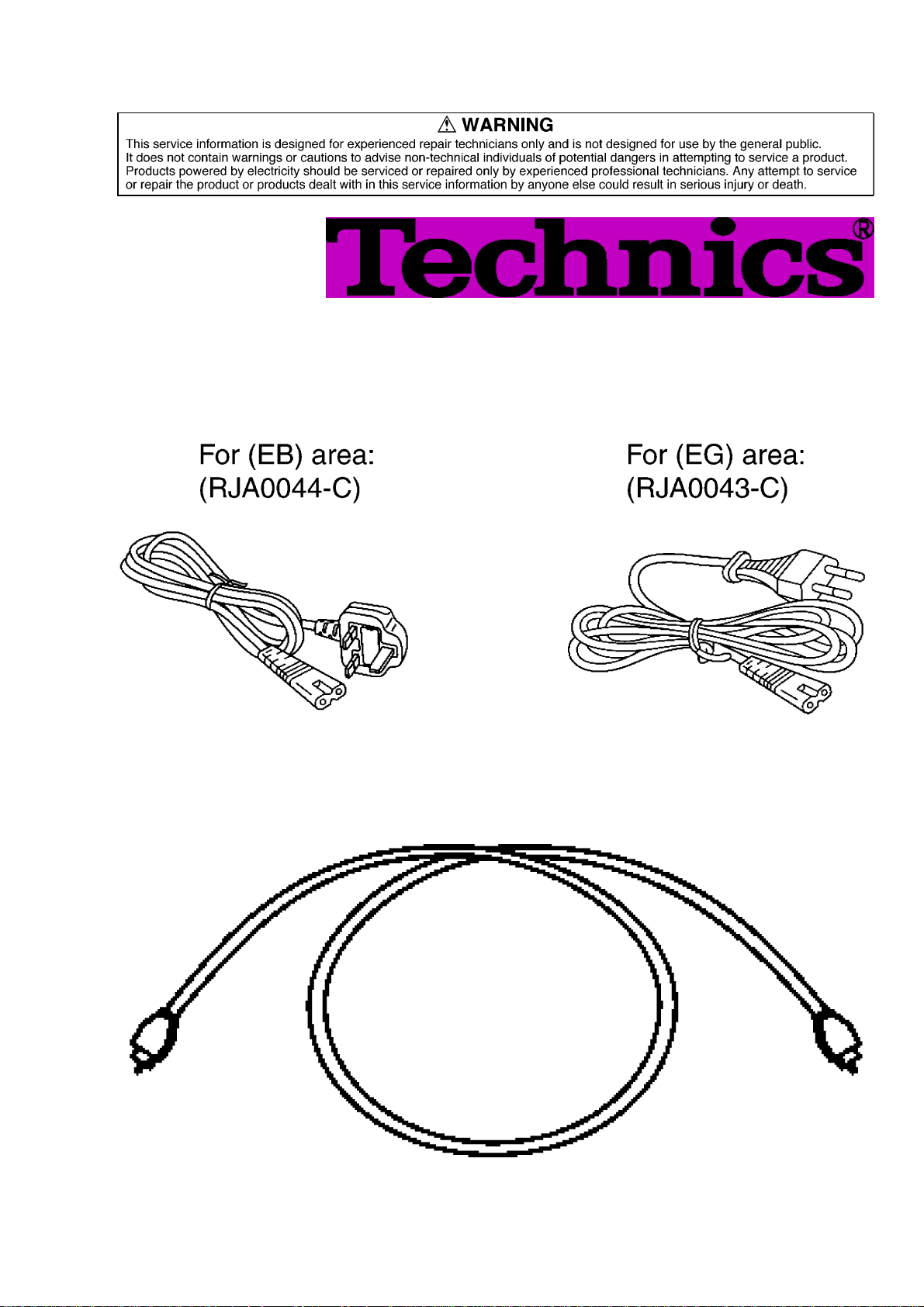
1. Accessories
-
AC power supply cord...............1pc.
-
Optical cable...............1pc.
(RJL1X001B05D)
3
Page 4
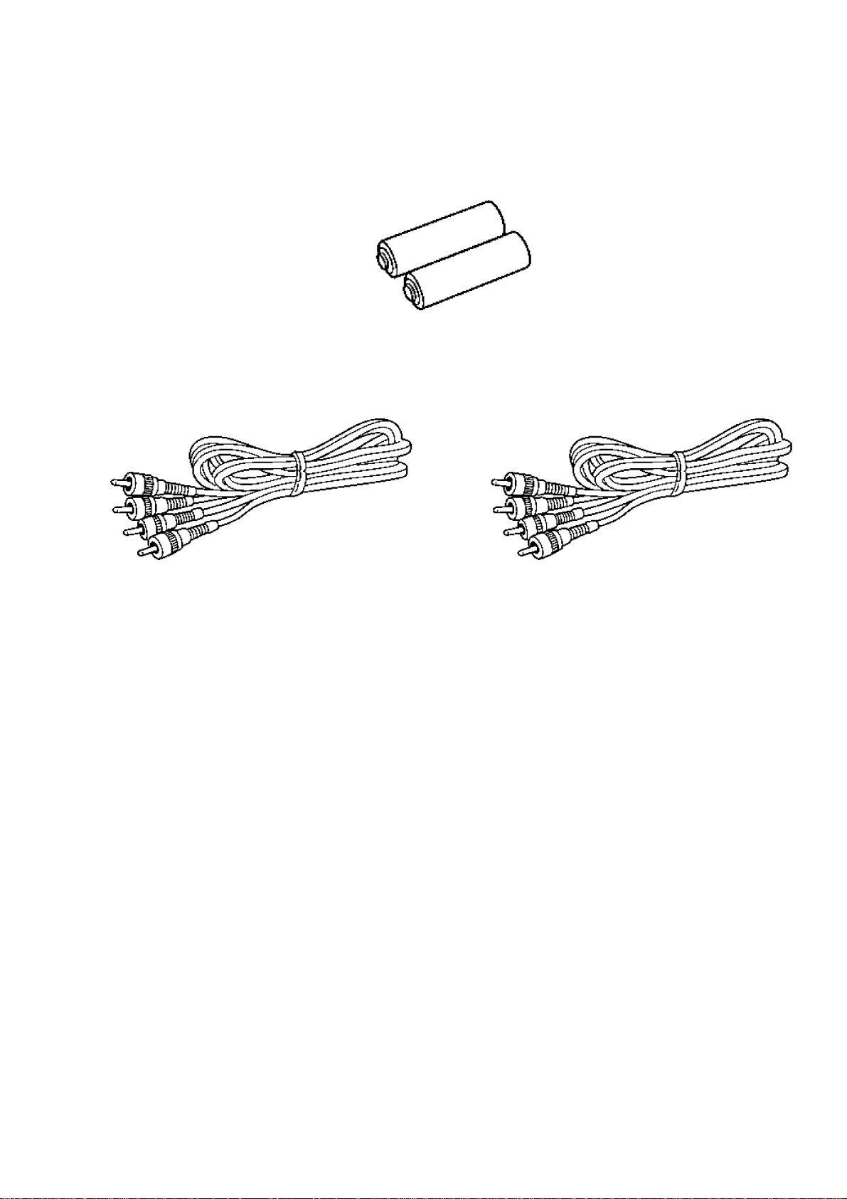
-
Remote control batteries...............2pcs.
[R6/LR6 (AA, UM-3) ]
Note:These are available on sales route.
-
Stereo phono cables...............2pcs.
(RJL2P004B08)
-
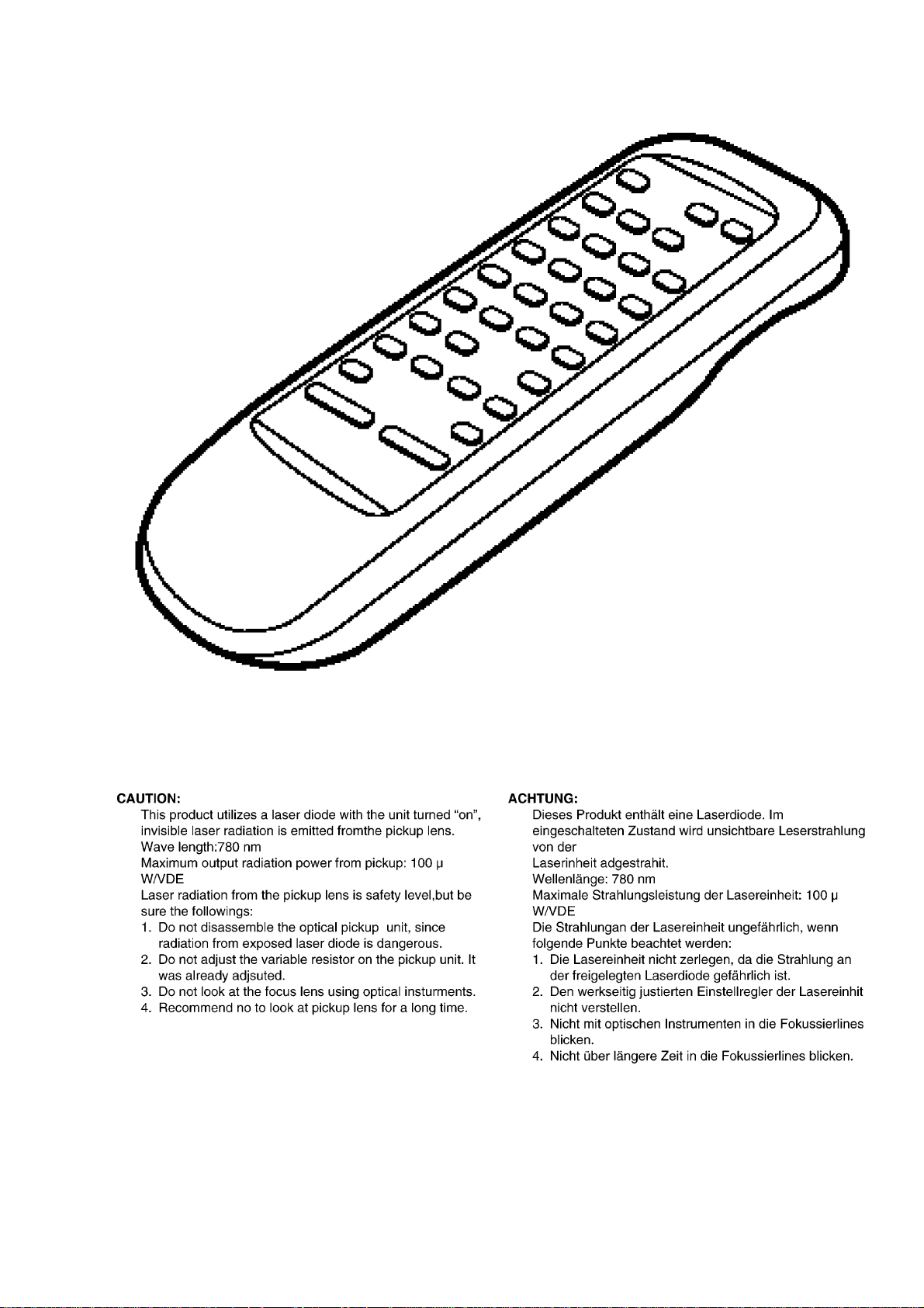
Remote control transmitter...............1pc.
(EUR645272)
4
Page 5
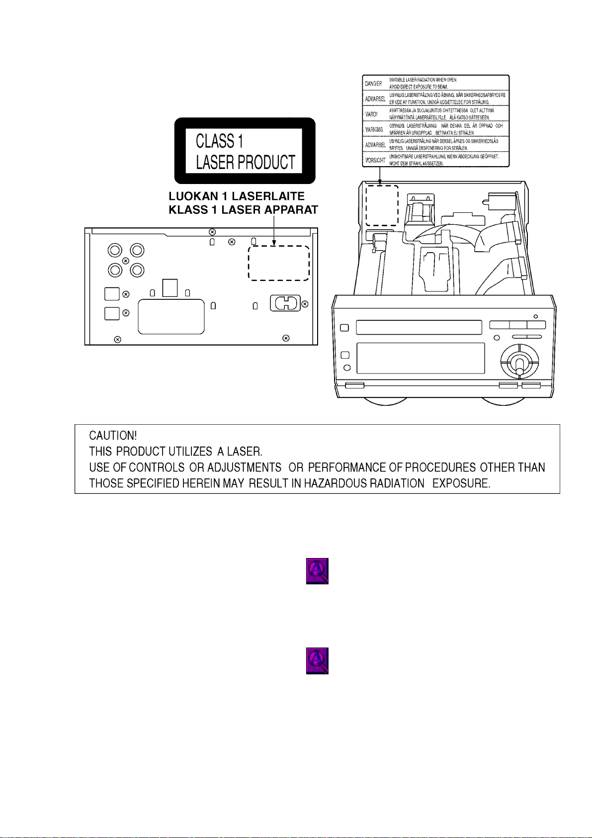
2. Precation of Laser Diode
5
Page 6
3. Caution for AC Main Lead
4. Operating Instructions
5. Handling Precautions for Traverse Deck (MD Unit)
The laser diode in the MD unit (optical pickup) may break down due to potential
difference caused by static electricity of clothes or human body.So, be careful of
6
Page 7
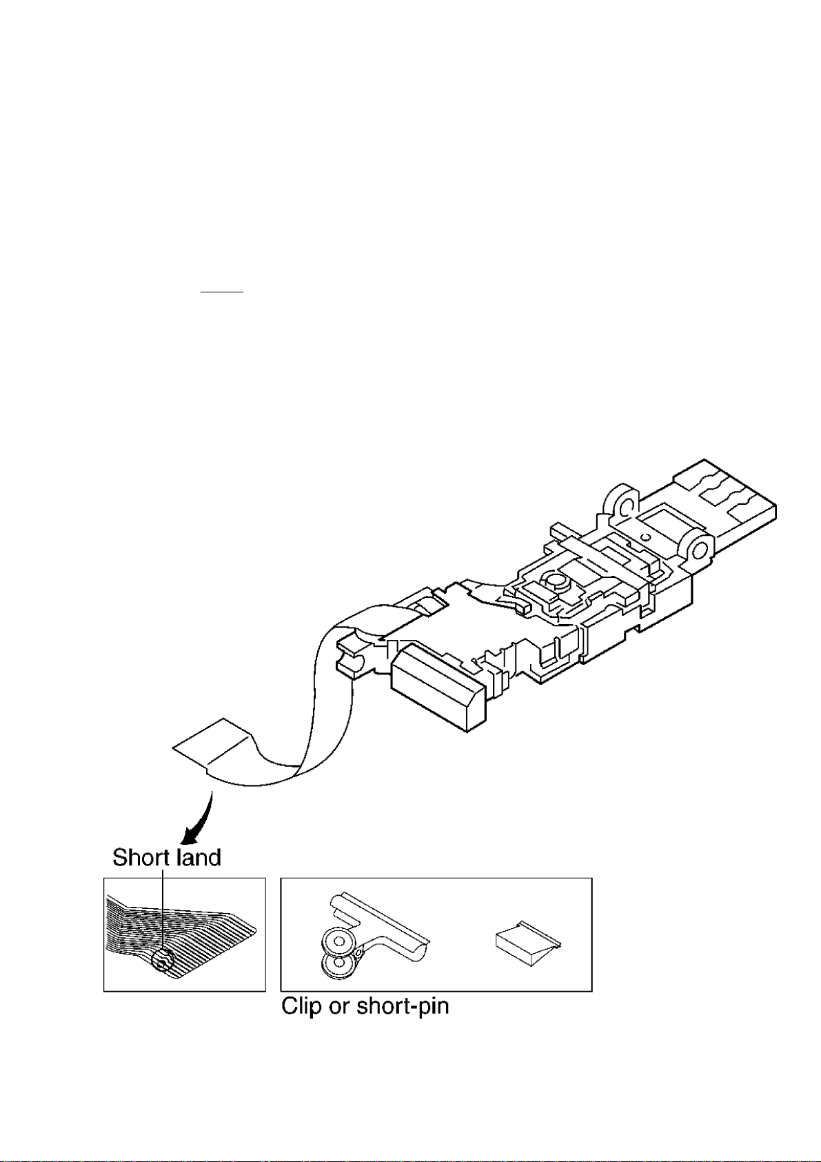
electrostatic breakdown during repair of the MD unit (optical pickup).
5.1. Handling of MD Unit (optical pickup)
1. Do not subject the MD unit (optical pickup) to static electricity as it is extremely
sensitive to electrical shock.
2. The short land between the No. 25 (LD-GND) and No. 24 (LD) pins on the flexible
board is shorted with a solder build-up to prevent damage to the laser diode. (As
shown in
To connect to the PC board, be sure to open by removing the solder build-up, and
finish the work quickly.
3. Take care not to apply excessive stress to the flexible board (FFC).
4. Do not turn the variable resistor (laser power adjustment). It has already been
adjusted.
Fig. 1.)
Fig. 1
7
Page 8
5.2. Grounding for electrostatic breakdown prevention
1. Human body grounding
Use the anti-static wrist strap to discharge the static electricity from your body.
(As shown in
2. Work table grounding
Put a conductive material (sheet) or steel sheet on the area where the optical
pickup is placed, and ground the sheet.
Caution:
The static electricity of your clothes will not be grounded through the wrist strap.
So, take care not to let your clothes touch the traverse deck (optical pickup).
Fig. 2.)
Fig. 2
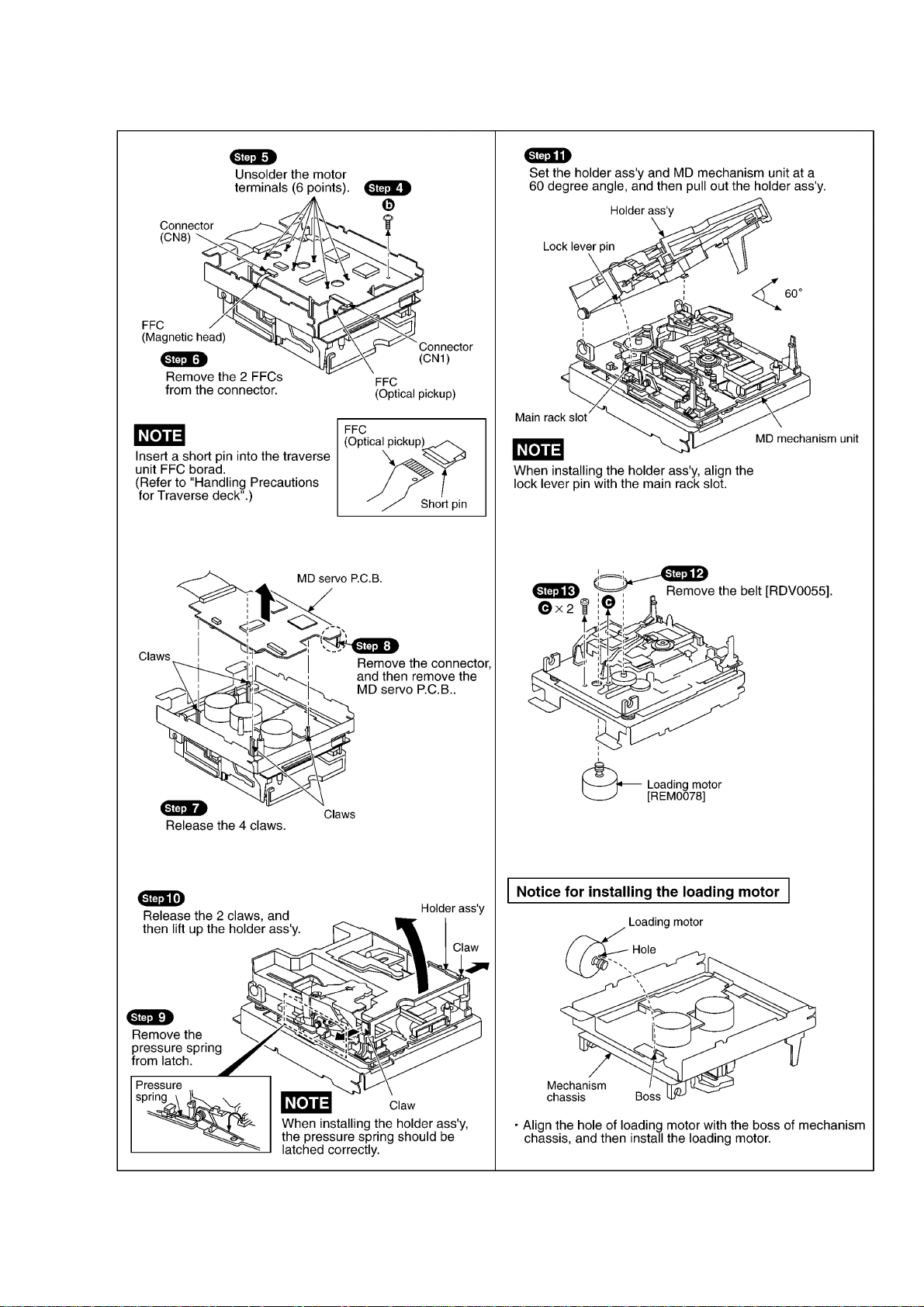
6. Operation Checks and Main Component Replacement
8
Page 9

Procedures
910111213
Page 10

Page 11

Page 12

Page 13
Page 14
14
Page 15

7. Self-Diagnostic Function
This unit is equipped with a self-diagnostic function which, in the event of a
malfunction, automatically display a code indicating the nature of the malfunction.
Use this self-diagnostic function when servicing the unit.
7.1. Switching to the Self-Diagnostic Mode
1. Turn the power on.
2. Press and hold the STOP button for at least 2 seconds, and while still pressing the
STOP button, press the FWD SEARCH button for at least 2 seconds. (Refer to
Fig.1.) The unit enters Self-Diagnostic Mode and is displayed “MD TEST”. Then an
error code is displayed, if any. For details of the error codes, refer to
Fig.2. In the
case of no errors, “
3. If more than one error exists, the display will sequentially show the respective
error codes each time the FWD SEARCH button is pressed.
----” is displayed on FL.
7.2. Canceling the Self-Diagnostic Mode
1. The Self-Diagnostic Mode can be canceled by pressing the POWER button
(POWER) to turn the system off. And then pressing the power button again to turn
it again.
7.3. Clearing the Self-Diagnostic Mode
1. The contents of abnormality display are stored in memory. In order to clear the
memory, continue to press the STOP button for at least 5 seconds while in the
Self-Diagnostic Mode. The memory will clear. Always be sure to clear this memory
after completing repair.
Fig.1
15
Page 16
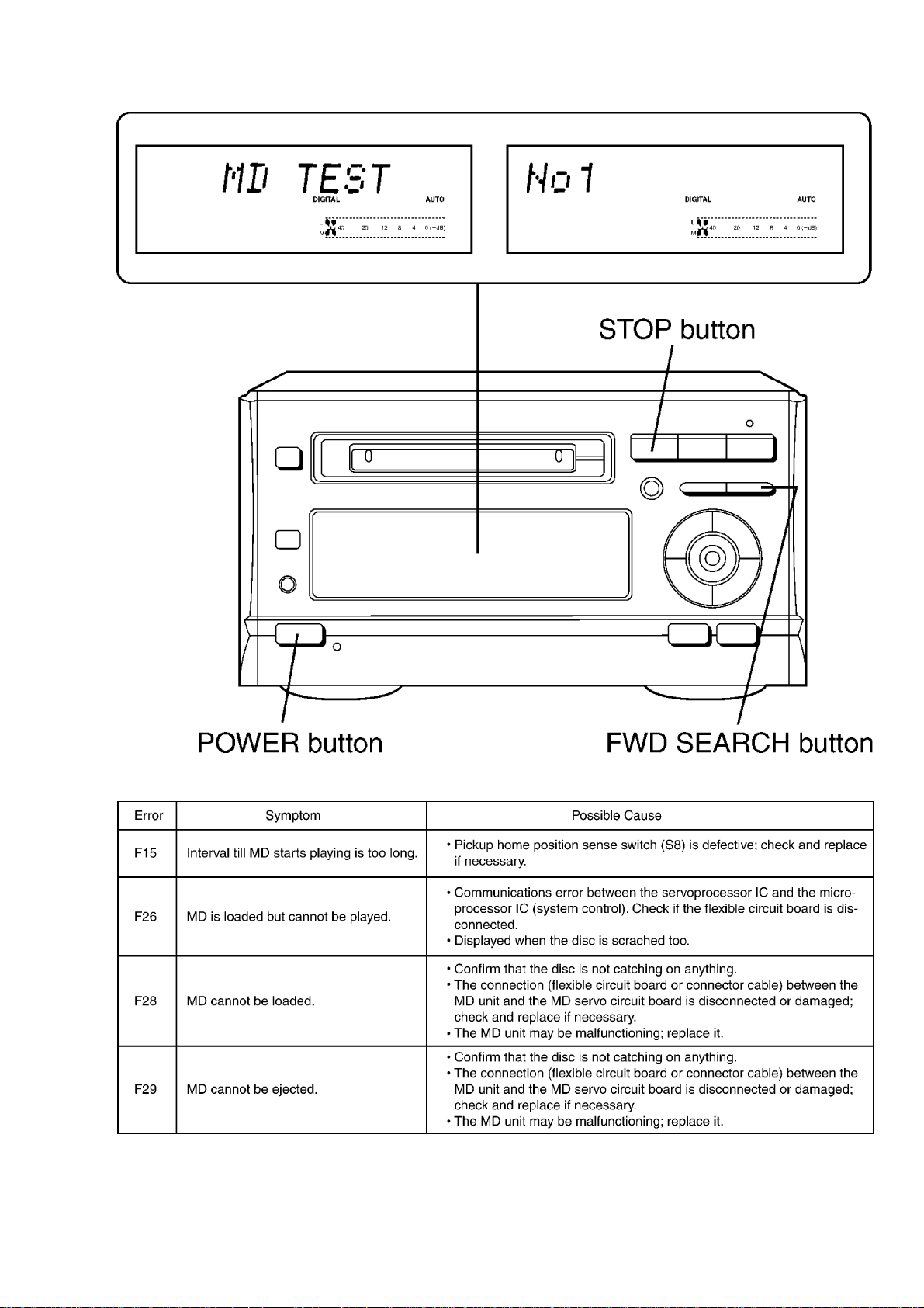
Fig.2
16
Page 17
8. Self Check Function
This unit is equipped with a self check function which can detect a part of
malfunction. Use this function before servicing the unit and check the item as shown
below.
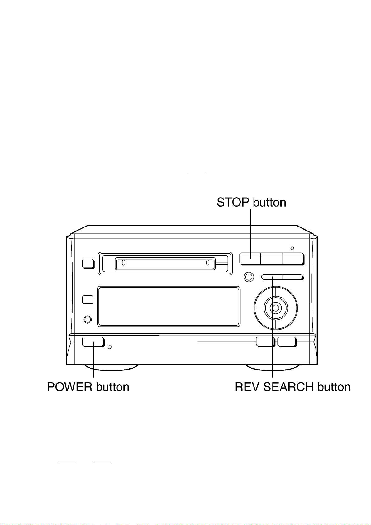
8.1. Setting to the Self Check Function
1. Turn the power on.
2. Press and hold the STOP button for at least 2 seconds, and while still pressing the
STOP button, press the REV. SEARCH button for at least 2 seconds. Then the unit
enters Self Check Function. (Refer to
Fig.3.)
Fig.3
8.2. Checking the operation switches
1. When the unit enters the Self Check Function, the FL display turn off.
2. Press the buttons on the unit except the INPUT SELECTOR button, it displays “-”
mark adapted each buttons.
(
Fig.4 and Fig.5 is shown about a allotment.)
17
Page 18
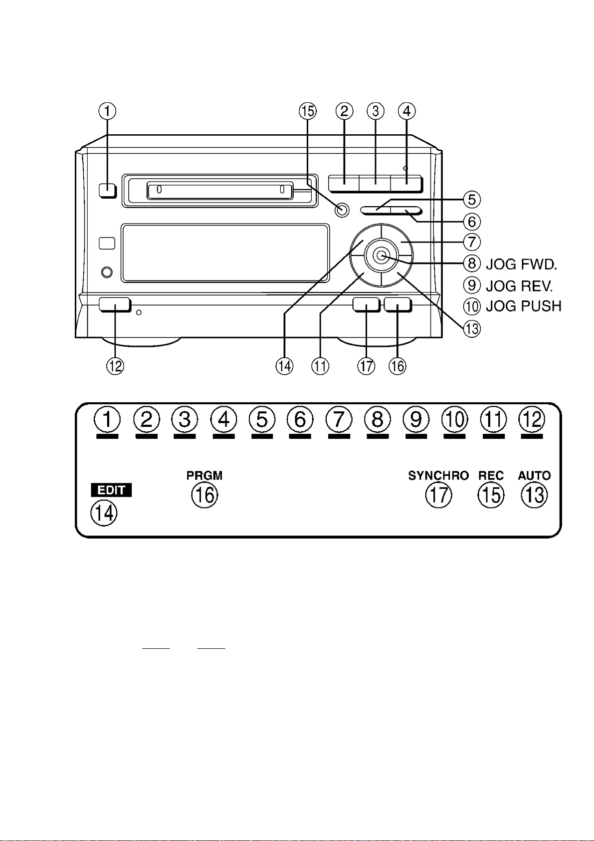
Fig.4
Fig.5
8.3. Checking the FL display
1. Press the INPUT SELECTOR button.
2. All buttons works normally except the POWER button, FL display and LED turns on
and off at 0.5 second interval.
(Refer to
Fig.6 and Fig.7.)
Fig.6
18
Page 19
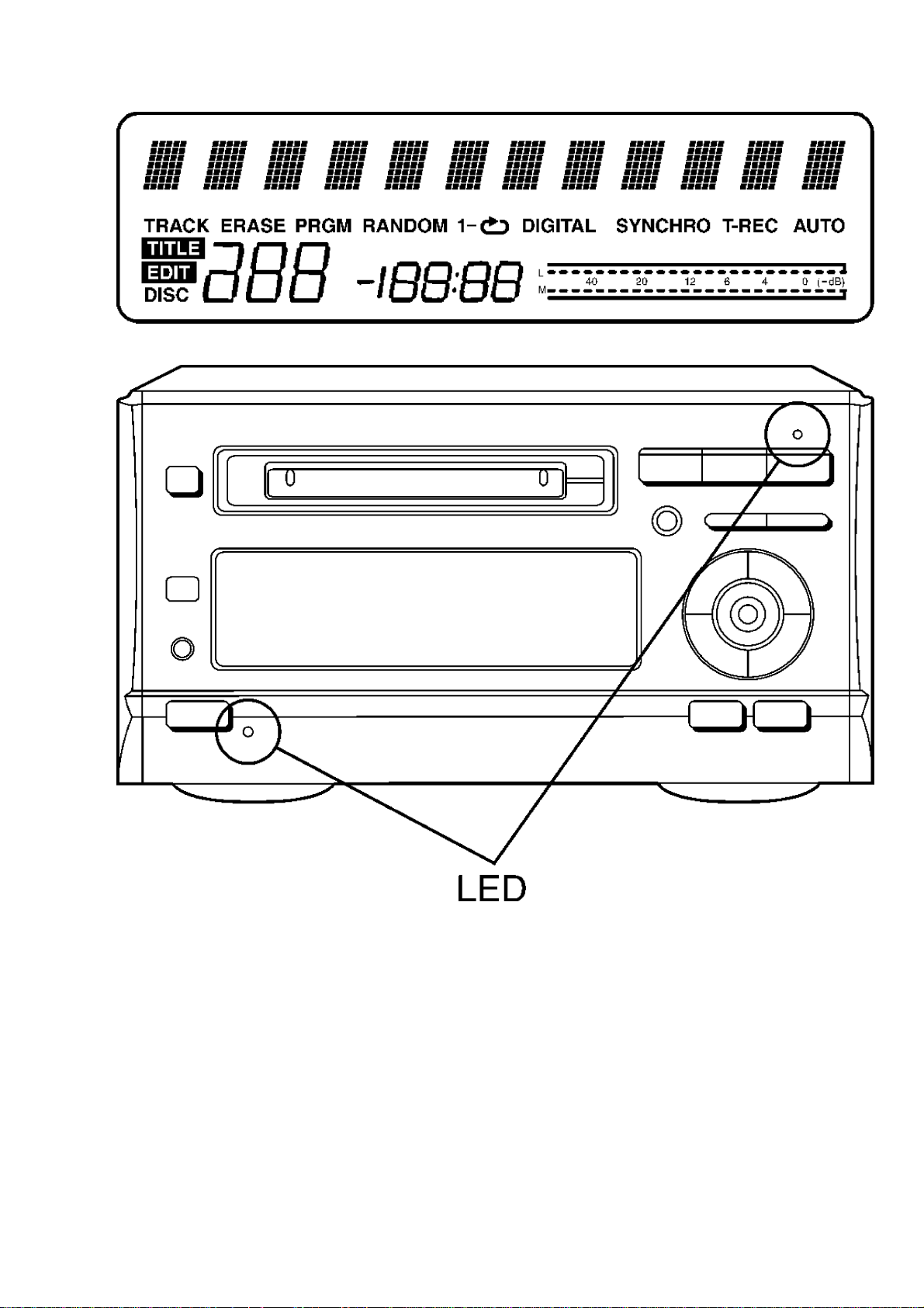
Fig.7
The Self Check Function can be canceled by pressing and holding the STOP
button for at least 2 seconds.
9. Measurements and Adjustments (Laser Power
Adjustment)
Note:
-
If you exchange parts of MD unit when you repair, you must perform the Laser
Power adjustment.
19
Page 20

-
Because this unit uses the optical magnetic recording, the unit outputs over 10
times more laser than a CD player does. In the adjustment mode, the laser is
always being output. Therefore, be especially careful not to look laser beam
directly or to touch the laser beam when adjusting the unit and checking its
operation.
9.1. Necessary Instruments
-
Laser power meter (LE8010) or cartridge type laser power meter
-
Test disc (Pre-mastered disc RFKV0006 or RFKV0014)
-
Recordable disc available on sales route (with music recorded)
-
Insulated driver for adjustment such as a ceramic driver
-
Remote control transmitter
9.2. Set the Unit to the Adjustmint Mode
1. Supply power to the unit.
2. With no MD loaded in the player, simultaneously press the [
[
seconds until “MD TEST” appears in the display. (Refer to
3. At the Self-Diagnostic Mode, press “1” on the player’s remote control. “RAM
LASER” will be displayed to indicate the read power adjustment mode.
FWD. SEARCH] button and hold them both pressed for at least 2
Fig.8
STOP] button and the
Fig.8.)
20
Page 21

Cautions
1. About handling the MD unit
- The magnetic head is a precision unit and is very fragile. Do not deform it.
- Laser diode in the optical pickup may be destroyed by the staticelectricity
generated in your clothes or body. Be especially careful with the static
electricity.
- The optical pickup is structured extremely precisely. Do not subject to the
strong impact or shock. Do not touch the lens.
2. About handling the magnetic head
When replacing the magnetic head, do not tighten the mounting screw (RHD17022)
too firmly. If the screw is tightened too much to deform the resin, the position of
the head is moved, and this affects its recording operation.
Recommended torque for mounting screw: 700 g cm +/- 100 g cm
Reference: This is the same force as using a screwdriver with a 15-mm diameter
grip, you fasten the screw naturally with your thumb and index finger.
3. About the driver for adjusting laser power
Use only insulated driver such as a ceramic driver. With the metal driver, it is not
possible to adjust properly because of the induction noise. Also, if it short-circuits
with the chassis, it may destroy or damage the laser diode.
Recommended driver: VESSEL 9000 1.8 -30 (Ceramic driver)
Cautions on optical pickup:
21
Page 22

-
The optical pickup and the magnetic head are structured precisely; therefore, they
are very fragile. Be careful not to touch them with the edge of the laser power
meter.
-
The sensor of the laser power meter is a very fine part. Be careful not to touch it to
the optical pickup lens.
-
The focus point of the laser reaches to 356°F. Therefore, avoid adjusting using
laser power for a long time because the sensor of the laser power meter may be
burned.
-
Do not allow the write power to even momentarily reach or exceed 5.5 mW. Doing
so will result in damage to the optical pickup.
-
Do not set the unit to the laser power adjustment mode with the MD loaded. Doing
so may result in damage to the MD.
9.3. Adjustment Procedure
Note:
There are two methods of adjusting the player, either by using a laser power meter or
by using a cartridge type laser power meter.
1. EntertheAdjustmentMode.
2. If using a laser power meter, slide open the sensor cover. (Refer to
Fig.9
3. If using a laser power meter, position the sensor directly above the optical pickup.
(Refer to
If using a cartridge type laser power meter, load the cartridge into the MD
Fig.10.)
Fig.9.)
22
Page 23

mechanism. (Refer to Fig.11.)
Caution:
Do not allow the laser power meter to come in contact with either the optical
pickup or the magnetic head.
Fig.10
Fig.11
23
Page 24

4. Confirm that the reading of the laser power meter or cartridge type laser power
meter is within the specified. If it is not within the specified range, adjust by
turning VR1. (Refer to
Specified range (read power): 600
Fig.12.)
µµµµ
W or lower
Fig.12
24
Page 25

Caution:
- Proceeding on to the subsequent adjustment procedure with the read power
exceeding 680
µµµµ
W will result in damage to the optical pickup.
5. Press “2” on the player’s remote control.
“WRITE LASER” will be displayed to indicate the write power adjustment mode.
6. Confirm that the reading of the laser power meter or cartridge type laser power
meter is within the specified range. If it is not within the specified range, adjust by
turning VR1. (Refer to
Fig.12.)
Specified range (write power): 4.8±0.1mW
Caution:
- Do not allow the write power to even momentarily reach or exceed 5.5mW. Doing so
will result in damage to the optical pickup.
7. Press “3” on the player’s remote control.
“ROM LASER” will be displayed to indicate the ROM data confirmation mode.
8. Confirm that the reading of the laser power meter or cartridge type laser power
meter is within the specified range.
Specified range (ROM data laser power): 540-660
µµµµ
W
9. Press “1” on the player’s remote control.
“RAM LASER” will be displayed to indicate the RAM data confirmation.
10. Confirm that the reading of the laser power meter or cartridge type laser meter is
within the specified range.
Specified range (RAM data laser power): 540-660
25
µµµµ
W
Page 26

- If the reading in either step 8 or 10 above is not within the specified range,
first switch off the power, and then reset the unit to the adjustment mode and
repeat the adjustment procedure.
10. Troubleshooting Guide
Please refer to this Troubleshooting Guide when you repair for any troubles of this
unit.
26272829303132
Page 27

Page 28

Page 29

Page 30

Page 31

Page 32

Page 33

33
Page 34

11. Schematic Diagram Notes
11.1. Schemtic Diagram Notes
This schematic diagram may be modified at any time with the development of new
technology.
Notes:
-
S1 : PROTECT det. switch.
34
Page 35

-
S2 : REFLECT det. switch.
-
S3 : LOAD OPEN det. switch.
-
S4 : DISC IN det. switch.
-
S5 : LOAD PLAY/REC det. switch.
-
S6 : LOAD PLAY det. switch.
-
S7 : LOAD TRG det. switch.
-
S8 : Traverse det. switch.
-
S901 : Standby/on ( ) switch.
-
S902 : Input selector (INPUT SELECTOR) switch.
-
S903 : Skip/Search ( ) switch.
-
S904 : Skip/Search ( ) switch.
-
S905 : Edit (EDIT) switch.
-
S906 : Enter (ENTER) switch.
-
S907 : Track mark mode select/character skip (TRACK MARKING/CHARA SKIP).
-
S908 : Display mode select/character (DISP/CHARA).
-
S909 : Eject ( EJECT) switch.
-
S910 : Stop ( ) switch.
-
S911 : Playback/Recording start ( ) switch.
-
S912 : Record ( REC) switch.
-
S913 : Pause ( ) switch.
-
S914 : Synchro-record (SYNCHRO REC) switch.
-
S915 : Playback mode (PLAY MODE) switch.
35
Page 36

-
VR1: Laser power adj. V.R..
-
VR901 : Input level/Jog push set V.R..
-
Indicated voltage values are the standard values for the unit measured by the DC
electronic circuit tester (high-impedance) with the chassis taken as standard.
Therefore, there may exist some errors in the voltage values, depending on the
internal impedance of the DC circuit tester.
No mark: MD STOP
( ): MD play [1kHz, L+R, 0dB]
<>: MD rec. [1kHz, L+R, 0dB]
Important safety notice:
Components identified by
Furthermore, special parts which have purpose of fire-retardant (resistors),
high-quality sound (capacitors), low-noise (resistors), etc. are used. When replacing
any of components, be sure to use only manufacture's specified parts shown in the
parts list.
mark have special characteristics important for safety.
Caution!
IC and LSI are sensitive to static electricity.
Secondary trouble can be prevented by taking care during repair.
Cover the parts boxes made of plastics with aluminum foil.
Ground the soldering iron.
Put a conductive mat on the work table.
Do not touch the legs of IC or LSI with the fingers directly.
Voltage and signal lines
: Positive voltage line
: Playback signal
: Recording signal
11.2. Type Illustration of IC's, Transistors and Diodes
36
Page 37

12. Schematic Diagram
13. Printed Circuit Board
14. Block Diagram
15. Wiring Connection Diagram
16. Terminal Function of IC's
16.1. IC1 (AN8772FHQ) : RF AMP
37
Page 38

Pin
No.
Mark I/O
Division
Function
1 CENVD — D signal det. capacitor
connection terminal
2 LDO O Laser amp output terminal
3 APCPD I Photo diode light quantity
det. input terminal
4 LD IN I Laser amp reverse input
terminal
5 APC REF I APC amp criterion voltage
input terminal
6 TEMP IN I Temperature sensor amp
input terminal
7 TEMP O Temperature sensor amp
output terminal
8 ADIP O ADIP signal output terminal
9 TOFS I Tracking error offset
adjustment terminal
10 TBAL I Tracking ballance
adjustment terminal
11 TE O Tracking error signal
output terminal
12 CRS IN I Track cross input terminal
13 TGAIN I Tracking gain adjustment
input terminal
14 LNP O Lens position signal
output terminal
15 AB GAIN I APP compensation signal
gain adjustment terminal
16 FE O Focus error signal output
terminal
17 AS GAIN I AS gain adjustment
terminal
18 FBAL I Focus ballance adjustment
terminal
19 AS/
MON3T
O AS/3TMON signal output
terminal
20 CEA I 3T envelope det. capacitor
connection terminal
21 BDO/
TRCRS
O BDO/Track cross signal
output terminal
22 CBD O O BDO detection capacitor
connection terminal
23 OFT O O Off track detection signal
output terminal
24 GND — GND terminal
25 OFT IN I Off track detection signal
input terminal
38
Page 39

Pin
No.
26 VCC I Power supply terminal
27
28 NRFLD I Serial command latch
29 RF DATA I Serial command data
30 RFCK I Serial command clock
31
32 OUT RF O EFM signal output terminal
33 CRF
34 EQ IN I EQ input terminal
35 ARFO O RF amp. output terminal
36 SVREF I Reference voltage input
37 VREF O Reference voltage output
38 RF1 I RF1 signal input terminal
39 RF2 I RF2 signal input terminal
40 F1 I F1 signal input terminal
41 F2 I F2 signal input terminal
42 CLPF1 — APP compensation LPF
43 CLPF2 — RF equalizer adjustment
44
~47
48 CENVC — Beam E signal detection
Mark I/O
NRFDET/
OFTR
NRFSTBY
AGC
A
~D
Function
Division
(+3V)
O NRFDET/off track signal
output terminal
signal input terminal
signal input terminal
input terminal
I Standby control signal
input terminal
— RFAGC capacitor
connection terminal
terminal
terminal
capacitor connection
terminal
resistor connection
terminal
I Beam A~D signal input
terminal
capacitor connection
terminal
16.2. IC2 (AN8814SB-E1) : FOCUS/TRACKING COIL,
SPINDLE/TRAVERSE MOTOR DRIVE
39
Page 40

Pin
No.
Mark I/O
Division
Function
1 REG B — 3.3V external transistor
control terminal (Not used,
open)
2 REG M — 3.3V regular output
monitor terminal (Not used,
connected to GND)
3 NC — Not used, open
4 OPO O Op-amp output terminal
5 OP- O Op-amp invert output
terminal
6 OP+ O Op-amp non-invert output
terminal (Not used,
connected to GND)
7 Vcc I Power supply terminal
8 1/2
PVcc2
O 1/2 PVcc output terminal 1
(Connected to GND
through capacitor)
9 PVcc2 I Power supply terminal for
driver
10 PGND2 — GND terminal
11 VO4- O Tracking coil driver output
terminal
12 VO4+ O Tracking coil driver output
terminal
13 VO3- O Focus coil driver output
terminal
14 VO3+ O Focus coil driver output
terminal
15 VO2- O Traverse motor drive
output terminal
16 VO2+ O Traverse motor drive
output terminal
17 VO1- O Spindle motor drive output
terminal
18 VO+ O Spindle motor drive output
terminal
19 PGND — GND terminal
20 PVcc1 I Power supply terminal
21 1/2 PVcc O 1/2 PVcc output terminal 1
(Connected to GND
through capacitor)
22 VREF I Reference voltage input
23 IN1 I Spindle motor drive input
terminal
24 PC1 I Power cut 1 input terminal
25 IN2 I Traverse motor drive input
40
Page 41

terminal
Pin
No.
26 PC2 I Power cut 2 input terminal
27 IN3 I Focus drive input terminal
28 IN4 I Tracking drive input
Mark I/O
Division
Function
terminal
16.3. IC3 (M6616RA1) : ATRAC ENCORDER/DECORDER, SERVO
SIGNAL PROCESSOR
Pin
No.
10 TOFS O Tracking off-set
11 FBAL O Focus balance adjustment
12 TBAL O Tracking balance
13 TGAIN O TE error gain adjustment
14 ASGAIN O Main beam amp gain
15 ABGAIN O APP adjustment output
16
17
Mark I/O
Division
1 ADIP I ADIP FM signal input
terminal
2 LNP I Lens position signal input
terminal
3 FE I Focus error signal input
terminal
4 TE I Tracking error signal input
terminal
5 AS I AS signal input terminal
6 DRMONI I Drive voltage monitor input
terminal
7 BAT I Battery power supply
terminal (Not used,
connected to GND)
8 AMONI — Servo analog monitor
signal output (Not used,
open)
9 VREFI I Reference voltage input
terminal
adjustment output terminal
output terminal
adjustment output terminal
output terminal
adjustment output terminal
terminal
AVDD1
AVSS1
I Power supply terminal
— GND terminal
Function
41
Page 42

Pin
No.
Mark I/O
Division
Function
18 FOD O Focus drive signal output
terminal
19 TRD O Tracking drive signal
output terminal
20 TVD O Traverse motor drive
signal ouutput terminal
21 SPD O Spindle motor drive signal
output terminal
22 SPON O Drive IC spindle ON signal
output terminal
23 TVON O Drive IC traverse ON signal
output terminal
24
DVDD0
I Power supply terminal
25 FG I FG input terminal
26 NRECT O Rec/Play switching signal
output terminal
27 IVDD2 — Power supply terminal for
I/O pad
28 IVDD0 — Power supply terminal for
I/O pad
29 DVss0 — GND terminal
30
~32
33
~42
43
~46
RAD12
~RAD10
RAD9
~RAD0
RDT3
~RDT0
— DRAM address output
terminal (Not used, open)
O DRAM address output
terminal
I/O DRAM data input/output
terminal
47 NRAS O DRAM row address strobe
output terminal
48 NCAS O DRAM culum address
strobe output terminal
49 NWE O DRAM write enable output
terminal
50 NRST I Reset signal input terminal
51 SELAD I MSP/MDA,I/F address
select input terminal (“H”
Address)
52 SSCK I MSP/MDA,I/F clock input
terminal
53 SSDW I MSP/MDA,I/F write data
input terminal
54 SSDR O MSP/MDA,I/F read data
output terminal
55 MDISY O Leader synchronous signal
output
56 SCTSY O ADIP synchronous noise
output terminal
42
Page 43

Pin
No.
Mark I/O
Division
Function
57 SGSYNC O Frame synchronous signal
output terminal
58 DVDD1 I Power supply terminal
59 IVDD1 — Power supply terminal for
I/O pad
60 DVss1 — GND terminal
61 FS384 O 384 Fs output terminal
62 SCL O Bit clock output terminal
63 SWS O Word clock output terminal
64 SDAP O Audio data output terminal
65 SDAR I Audio data input terminal
66 LRCK I CD word clock input
terminal (Connected to
GND)
67 BCK I CD bit clock input terminal
(Connected to GND)
68 DATA I CD data input terminal
(Connected to GND)
69 TX O Digital audio interface
signal output terminal (Not
used, open)
70 RX1 I Digital audio interface
signal 1 input terminal
71 RX2 I Digital audio interface
signal 2 input terminal
72 NREFM — EFM modulation inverted
output (Not used, open)
73 REFM O EFM modulation output
terminal
74 MONI3 — Monitor signal output (Not
used, open)
75 MONI2 — Monitor signal output (Not
used, open)
76 MONI1 — Monitor signal output (Not
used, open)
77 MONI0 — Monitor signal output (Not
used, open)
78 TS3 — Not used, connected to
GND
79 TS2 — Not used, connected to
GND
80 TS1 — Not used, connected to
GND
81 TS0 — Not used, connected to
GND
43
Page 44

Pin
No.
82
83 DVDD2 I Power supply terminal
84 XI I Crystal oscillator input
85 XO O Crystal oscillator output
86 VDss2 — GND terminal
87 RFDAT O RF serial data output
88 RFCK O RF serial clock output
89 NRFLD O RF serial load output
90 TRCRS I Track cross input terminal
91 OFTR I Off-track signal input
92 APCD O Laser power PWM output
93
94 PEFM1 O EFM loop filter output
95 EFMIREF I EFM PLL reference current
96
97 PEFMS I EFM signal input terminal
98
99 AVss0 — GND terminal
100 TEFSEL — Not used, open
Mark I/O
EXSYSCK
EXEFMCK
EFMPLLF
AVDD0
Function
Division
— External system clock
input terminal (Not used,
connected to GND)
terminal (F=16.9344MHz)
terminal (F=16.9344MHz)
terminal
terminal
terminal
terminal
terminal
I External FM clock input
terminal (Not used,
connected to GND through
registor)
terminal
input terminal
O EFM PLL filter output
terminal
I Power supply terminal
16.4. IC10 (MN101D03DAA) : SYSTEM CONTROL
44
Page 45

Pin
No.
Mark I/O
Division
Function
1 DACRST O DAC reset signal output
terminal to IC4 (“L”:Reset)
2 DEO O DE emphasis signal output
terminal to IC4(“L”:DE
emphases)
3 MUTE — AD-DA mute output
terminal (Not used, open)
4 AD RST O Reset signal output
terminal
5
NRFSTBY
O Standby control signal
output terminal
(“L”:Standby)
6 PC O Transistor drive signal
output terminal (“H”:Power
ON)
7 MSP
RST
O MSP reset signal output
terminal (“L”:Reset)
8 LOAD1 O Loading motor drive 1
output terminal
9 LOAD0 O Loading motor drive 0
output terminal
10 NEFMON O Magnetic head current
output terminal
11 TEST01 O Test signal output terminal
(Not used, open)
12 TVSW I Traverse innermost
detection switch signal
input terminal
13 DISC IN I Disc detection switch
signal input terminal
14
REFLECT
I Reflection rate switch
signal input terminal
15 LOAD
SW0
(OPEN)
16 LOAD
SW1
(TRG)
17 LOAD
SW2
(PLAY/REC)
18 LOAD
SW3
(PLAY)
19
PROTECT
I Loading mechanism
position det. Switch 0
signal input terminal
I Loading mechanism
position det. Switch 1
signal input terminal
I Loading mechanism
position det. Switch 2
signal input terminal.
I Loading mechanism
position det. Switch 3
signal input terminal
I Erase prevention switch
signal input terminal
20 MMOD — Connected to GND
45
Page 46

20
MMOD
—
Connected
to
GND
46
Page 47

Pin
No.
Mark I/O
Division
Function
21 RST I Reset signal input terminal
(“L”:Reset)
22 UNIT
TEST
I Test signal input terminal
(Open)
23 CS2 I Test signal input terminal
(Open)
24 SCTSY I Micro computer interrupt
signal input terminal
(SUBQ/ADIP simultaneous
signal)
25 MDISY I Micro computer interrupt
signal input terminal (MD
simultaneous signal)
26 PANEL
REQ
27
~29
LED
OUT1
~LED
I Panel I/F request signal
input terminal
O Drive signal output
terminal to LED DRIVE
(“H”:LED ON)
OUT3
30 TEST02 O Test signal output terminal
(Not used, open)
31
VDD2(3V)
I Power supply terminal
(+3V)
32 OSC1 I Crystal oscillator input
terminal (f=10MHz)
33 OSC2 O Crystal oscillator output
terminal (f=10MHz)
34
V
SS
— GND terminal
35 XI I Not used, connected to
GND
36 XO O Not used, open
37 VSS — GND terminal
38 TEST03 O Test signal output terminal
(Not used, open)
39 EEPCS O EEPROM chip select signal
output terminal (Not used,
open)
40 EEPCK O EEPROM clock signal
output terminal (Not used,
open)
41
EEPDATA
I/O EEPROM data in/output
terminal (Connected to
GND through resistor)
42 TEST04 O Test signal output terminal
43 TEST05
(Not used, open)
44 CFSYNC I ATRACK management
frame simultaneous signal
input terminal
47
Page 48

input
terminal
Pin
No.
Mark I/O
Division
Function
45 TEST06 O Test signal output terminal
(Not used, open)
46 TEST07 I Connected to rec/play
switch signal
47 TOK OK O Not used, open
48 HF ON — Drive signal output
terminal to Q3 (POWER
SUPPLY CONTROL)
49 PANEL
CLK
50 PANEL
I Panel I/F clock input
terminal
I Panel I/F data input terminal
DATA I
51 PANEL
DATA 0
52 PANEL
CS
O Panel I/F data output
terminal
O Panel I/F chip select output
terminal
53 SELAD O Micro computer I/F address
select output terminal
54 SSCLK O Micro computer I/F clock
output terminal
55 SSDR I Micro computer I/F reading
data input terminal
56 SSDW O Micro computer I/F writing
data output terminal
57 LCDCK O LCD clock test signal
output terminal
(Connected to power
supply through resistor)
58 ADRS
TEST
RXD
59 LCD
DATA
O Test signal output terminal
(Connected to power
supply through resistor)
O Test signal output terminal
(Not used, open)
TXD
60 VREF- — Connected to GND
61 TEMP I Temprature sensor amp
input terminal
62 KEY1 I Key input 1 terminal
63 KEY2 I Key input 2 terminal
64 NO
LOAD
I Test signal input terminal
(“L”:Without loading
mechanism) (Open)
65
SRVTEST
I Test signal input terminal
(“L”:Servo test mode)
(Open)
66 LOAD P I Test signal input terminal
(Open)
48
Page 49

Pin
No.
67 TEST
68 SRV
69 VCC 3V I Power supply terminal
70 VCC 5V I Power supply terminal
71
72 SLOCK O Spindle lock test signal
73 TLOCK O Tracking lock signal output
74 FLOCK O Focus lock test signal
75 ERROR O Servo error test signal
76 BUSY O Servo busy test signal
77
78
79
80 SPMWE O SPM take in test signal
Mark I/O
KEY IN
LOAD
SELADDA
SBPRETRY
SRVRETRY
ARDSKIP
Function
Division
I Test signal input terminal
(“L”:Unit key mode) (Open)
I Test signal input terminal
(“L”:Using for servo
primary values EEPROM)
(+3V)
(+5V)
I AD/DA converter select
signal input terminal (Open)
output terminal (Not used,
open)
terminal (“H”:lock) (Not
used, open)
output terminal (“H”:lock)
(Not used, open)
output terminal (Not used,
open)
output terminal (Not used,
open)
O Signal management retry
test signal output terminal
(Not used, open)
O Servo retry test signal
output terminal (Not used,
open)
O Address skip test signal
output terminal (Not used,
open)
output terminal (Not used,
open)
16.5. IC72 (MNV4400-T8T) : 4M DRAM
49
Page 50

Pin
No.
10
~12A1~A3
13 VCC I Power supply terminal
14
~18A4~A8
22 OE I DRAM output enable input
23 CAS I DRAM calam address
24 DO3 I/O DRAM data 3 in/output
25 DO4 I/O DRAM data 4 in/output
26 VSS — GND terminal
Mark I/O
Division
1 DO1 I/O DRAM data 1 in/output
terminal
2 DO2 I/O DRAM data 2 in/output
terminal
3 WE I DRAM light enable input
terminal
4 RAS I DRAM low address strobe
input terminal
5 A9 I DRAM address 9 input
terminal
9 A0 I DRAM address 0 input
terminal
I DRAM address 1~3 input
terminal
I DRAM address 4~8 input
terminal
terminal (Not used,
connected to GND)
strobe input terminal
terminal
terminal
Function
16.6. IC901 (M30218MAA106): FL DRIVE/SYSTEM CONTROL
50
Page 51

Pin
No.
Mark I/O
Division
Function
1 P97 O VR control clock output
terminal
2 P96 O VR control data output
terminal
3 P95 O VR control STB output
terminal
4 P94 O Digital in 1/2 select signal
output terminal (“H”: in 1)
5 P93 I Not used, connected to
GND
6 P92 I Chip select input terminal
7 P91 O Request signal output
terminal
8 P90 O Reset signal output
terminal
9 CNVSS — Flash write signal voltage
(Connected to GND
through resistor)
10 P87 O Power on/off control signal
output terminal
11 P86 — Not used, connected to
GND
12 RESET I Reset signal input terminal
13 XOUT O Clock ceramic oscillator
output terminal (f=10MHz)
14 VSS — GND terminal
15 XIN I Clock ceramic oscillator
output terminal (f=10MHz)
16 VCC I Power supply terminal
17 P85 I AC detect terminal
18 P84 I Remote control data input
terminal
19 P83 I Unit load switch signal
input terminal
20 P82 O Audio mute signal output
terminal
21 P81 O Play LED drive signal
22 P80
output terminal (“L”: LED
on)
23 P77 I Not used, connected to
power supply through
resistor
24 P76 O Communication clock
output terminal
25 P75 I Data input terminal
26 P74 O Data output terminal
51
Page 52

Pin
No.
27
~30
Mark I/O
Division
P73
I Not used, connected to
~P70
Function
power supply through
resistor
31
~34
P47
~P44
— Not used, connected to
power supply through
resistor
35 P43 — Not used, connected to
GND
36 P42 I Model select terminal
37 P41 O FL segment control signal
38 P40
39
~46
47
~62
P37
~P30
P27
~P10
output terminal
63 VCC I Power supply input
terminal
64 P07 O FL segment control signal
output terminal
65 VSS — GND terminal
66
~72
P06
~P00
O FL segment control signal
output terminal
73 P57
74 P56 O Q905 drive signal output
terminal
75 P55 Q904 drive signal output
terminal
76 P54 Q903 drive signal output
terminal
77
~80
81
~88
P53
~P50
P67
~60
O FL grid control signal
output terminal
89 -VP I Power supply input
terminal
90 P107/
AN7
I Not used, connected to
GND
91 P106/
AN6
92 P105/
I Key switch input terminal
AN5
93 P104/
AN4
94
~96
P103/
AN3
— Not used, connected to
GND
~P101/
AN1
52
Page 53

Pin
No.
97 AVSS — GND terminal
98 P100/
99 VREF I Referance voltage input
100 AVCC I Power supply input
Mark I/O
Division
— Not used, connected to
AN0
Function
GND
terminal
terminal
17. Replacement Parts List
Notes:
*Important safety notice:
Components identified by
Funrthermore, special parts which have purposes of fire-retardant (resistors),
high-quality sound (capacitors), low-noise (resistors), etc. are used.
When replacing any of components, be sure to use only manufacture’s specified
parts shown in the parts list.
*Warning: This product uses a laser diode. Refer to caution statements.
*ACHTUNG:Die lasereinheit nicht zerlegen.Die lasereinheit darf nur gegen einc vom
hersteller spezifizierte einheit ausgetauscht werden.
*Capacity values are in microfarads (uF) unless specified otherwise, P=Pico-farads
(pF) F=Farads (F)
*Resistance values are in ohms, unless specified otherwise, 1K=1,000 (OHM),
1M=1,000K (OHM)
*[MAVD] indicates in Remarks colums parts that are supplied by MAVD.
*The marking <RTL> indicates that the Retention Time is limited for this item. After
the discontinuation of this assembly in production, the item will continue to be
available for a specific period of time. The retention period of availability is
dependant on the type of assembly , and in accordance with the laws governing part
and product retention. After the end of this period, the assembly will no longer be
available.
*“<IA>”, “<IB>”, “<IC>”, marks in Remarks indicate languages of instruction
manuals. [<IA> : English, <IB> : German / Italian / French, <IC> : Netherlands / Danish
/ Spanish / Swedish / Polish]
mark have special characteristics important for safety.
53
Page 54

Ref. No.
1 RGK1148-M
2 RGK1149-M SIDE PANEL(R) 1
3 RHD30073-K SCREW 4
4 RKM0326G-S CABINET 1 [MAVD]
5 XTBS3+8JFZ1 SCREW 1
6 REZ1250 FFC(30P) 1 [MAVD]
7 REZ1251 FFC(20P) 1 [MAVD]
8 RKA0076-N3 FOOT 4
8-1 RKA0083-K CUSHION 4
9 XTB3+6G SCREW 4
10 RGK0810-N3 SIDE ORNAMENT(L) 1
11 RGK0811-N3 SIDE ORNAMENT(R) 1
12 RGK0886-1H MD LID 1
13 RGL0345-Q LED INDICATOR 1
14 RGG0139C-S FRONT PANEL 1 [MAVD]
15 RGL0455-Q INDICATOR 1 [MAVD]
16 RGP0573A-S1 SUB PANEL 1 [MAVD]
17 RGU1471A-S BUTTON POWER 1 [MAVD]
18 RGU1472-S BUTTON PLAY 1
19 RGU1473-S BUTTON ENTER 1
20 RGU1474A-S BUTTON DISPLAY MODE 1 [MAVD]
21 RGU1475-S BUTTON EJECT 1
22 RGW0254-S KNOB JOG 1
23 RHD20010 SCREW 2
24 RHD26021 SCREW 5
25 RHN70002 NUT 1
26 RKW0482A-Y FL WINDOW 1
27 RKW0483-Q REMOTE SENSOR WINDOW 1
28 RMB0495 SPRING 1
29 RMG0387A-K RUBBER 1
30 XTBR3+20JFZ SCREW 2
31 XTBS3+8JFZ1 SCREW 12
100 RED0047-1 MAGNETIC HEAD 1
101 RHD17021 SCREW 1
102 RHD17022 SCREW 1
103 RMC0348 THRUST SPRING 1
104 RMC0349 NUT PLATE SPRING 1
105 RML0515 HEAD SIFTER 1
106 RMQ0750 REF BASE 1
107 RMQ0751 NUT PLATE 1
108 RMS0611 MAIN SHAFT 1
109 RXJ0021 DRIVE SHAFT 1
110 RXK0249 MECHANISM CHASSIS 1
110-1 RDV0055 BELT 1
110-2 REM0077 TRAVERSE MOTOR 1
110-3 REM0078 LOADING MOTOR 1
110-4 RMB0548 PRESSURE SPRING 1
110-5 RMQ0752 DETECTOR PIN(1) 1
110-6 RMQ0753 DETECTOR PIN(2) 2
110-7 XQN17+C25FZ SCREW 6
110-8 XYC2+FF105 SCREW 1
111 RAF1700A OPTICAL PICKUP 1
112 XTW2+6S SCREW 1
113 RHD20053 SCREW 4
114 RMB0504 SPRING 4
115 RMG0447-K DAMPER 4
Part No.
Part Name & Description Pcs Remarks
SIDE PANEL(L)
1
54
Page 55

Ref. No.
116 XTN17+6GFZ SCREW 1
117 RMR1118-K2 HOLDER 1
A1 EUR645272 REMOTE CONTROLLER 1 [MAVD]
A1-1 UR64EC1987B BATT.COVER(REMOTE CONT.) 1
A2 RJA0044-C AC POWER SUPPLY CORD 1 (EB)[MAVD]
A2 RJA0043-C AC POWER SUPPLY CORD 1 (EG)
A3 RJL1X001B05D OPTICAL CABLE 1
A4 RJL2P004B08A RCA PIN CORD 2
A5 RQA0117 WARRANTY CARD 1
A6 RQCB0169 SERVICENTER LIST 1
A7 RQT5092-1B INSTRUCTION MANUAL 1 <IA>[MAVD]
A7 RQT5093-D INSTRUCTION MANUAL 1 (EG)<IB>[MAVD]
A7 RQT5094-E INSTRUCTION MANUAL 1 (EG)<IC>[MAVD]
C1 ECUV1H221KBV 50V 220P 1
C4 ECUVNA105ZFV 10V 1U 1
C5 ECUVNA224KBV 10V 0.22U 1
C6 ECUVNA105ZFV 10V 1U 1
C7,8 ECUVNA224KBV 10V 0.22U 2
C11 ECUVNE223KBV 25V 0.022U 1
C12 ECUV0J474KBV 6.3V 0.47U 1
C13 ECUV1C393KBV 16V 0.039U 1
C14 ECUV1H102KBV 50V 1000P 1
C15 ECST0GY106RR 4V 10U 1
C16 ECUV1H181KV 50V 180P 1
C17 ECUV1H332KBV 50V 3300P 1
C18 ECUV1H562KBV 50V 5600P 1
C19 ECUVNC104ZFV 16V 0.1U 1
C20 ECST0GY106RR 4V 10U 1
C21 ECUV1H822KBV 50V 8200P 1
C22 ECUV1H102KBV 50V 1000P 1
C23 ECUVNC104ZFV 16V 0.1U 1
C24 ECUV1H102KBV 50V 1000P 1
C25 ECUV1C393KBV 16V 0.039U 1
C26 ECUV1H472KBV 16V 4700P 1
C28 ECST0GY226RR 4V 22U 1
C29 ECUV1H332KBV 50V 3300P 1
C30 ECUV1E123KBV 25V 0.012U 1
C31,32 ECUV1H102KBV 50V 1000P 2
C33 ECST0GY106RR 4V 10U 1
C34,35 ECUV1H102KBV 50V 1000P 2
C37 ECUV1H181KV 50V 180P 1
C40 ECUVNC104ZFV 16V 0.1U 1
C41 ECEV0JA331P 6.3V 330U 1
C42 ECST0GY106RR 4V 10U 1
C45 ECST0GY106RR 4V 10U 1
C46 ECUVNC104ZFV 16V 0.1U 1
C47 ECUVNA105ZFV 10V 1U 1
C48 ECUVNC104ZFV 16V 0.1U 1
C50 ECUVNC104ZFV 16V 0.1U 1
C51,52 ECUVNA105ZFV 10V 1U 2
C53 ECUV1H332KBV 50V 3300P 1
C55-58 ECUV1H102KBV 50V 1000P 4
Part No.
Part Name & Description Pcs Remarks
55
Page 56

Ref. No.
C59 ECUV1C823KBV 16V 0.082U 1
C60 ECEV1CA100NR 16V 10U 1
C61 ECUVNJ334KBV 63V 0.33U 1
C62 ECUV1H221KBV 50V 220P 1
C64 ECUVNE153KBV 25V 0.015U 1
C65 ECUVNC104KBV 16V 0.1U 1
C66 ECUV1C823KBV 16V 0.082U 1
C67 ECUV1H392KBV 50V 3900P 1
C70 ECUV1E123KBV 25V 0.012U 1
C71-76 ECUVNC104ZFV 16V 0.1U 6
C79,80 ECUVNC104ZFV 16V 0.1U 2
C81 ECUV1H560JCV 50V 56P 1
C82 ECUVNC473KBV 16V 0.047U 1
C83,84 ECUVNC104ZFV 16V 0.1U 2
C85 ECST0GY106RR 4V 10U 1
C86 ECUVNE153KBV 25V 0.015U 1
C87 ECUVNC104ZFV 16V 0.1U 1
C88,89 ECUV1H331KBV 50V 330P 2
C90,91 ECUV1H080DCV 50V 8P 2
C92,93 ECUVNC104ZFV 16V 0.1U 2
C94 ECST0GY475RR 4V 4.7U 1
C95 ECUVNC104ZFV 16V 0.1U 1
C96,97 ECST0GY475RR 4V 4.7U 2
C98 ECUVNC104ZFV 16V 0.1U 1
C99 ECUV1H102KBV 50V 1000P 1
C100 ECUVNC104ZFV 16V 0.1U 1
C101 ECST0GY106RR 4V 10U 1
C102 ECUVNC104ZFV 16V 0.1U 1
C103 ECST0GY106RR 4V 10U 1
C106 ECUV1H102KBV 50V 1000P 1
C110 ECUVNC104ZFV 16V 0.1U 1
C111 ECST0GY106RR 4V 10U 1
C112 ECEV1CA100NR 16V 10U 1
C113 ECUVNC104ZFV 16V 0.1U 1
C114,15 ECUV1H561KBV 50V 560P 2
C117 ECEV0JA331P 6.3V 330U 1
C118 ECUVNA105KBN 10V 1U 1
C119 ECUV1H102KBV 50V 1000P 1
C120 ECUV1H560JCV 50V 56P 1
C121 ECUV1H102KBV 50V 1000P 1
C122 ECUVNA105ZFV 10V 1U 1
C123 ECUVNC104ZFV 16V 0.1U 1
C128 ECUVNC104ZFV 16V 0.1U 1
C129 ECUV1H101JCV 50V 100P 1
C133 ECUVNA105ZFV 10V 1U 1
C134 ECUV1H331KBV 50V 330P 1
C138 ECEV0JA470SR 6.3V 47U 1
C139-42 ECUVNC104ZFV 16V 0.1U 4
C143 ECST0GY106RR 4V 10U 1
C144 ECUVNH103KBV 50V 0.01U 1
C147-49 ECUVNH103KBV 50V 0.01U 3
C154,55 ECUV1H330GCV 50V 33P 2
C301 ECBT1H104ZF5 50V 0.1U 1
C302 ECA1CM103E 16V 1000U 1
C303 ECBT1H104ZF5 50V 0.1U 1
C304-06 ECA1HM101 50V 100U 3
Part No.
Part Name & Description Pcs Remarks
56
Page 57

Ref. No.
C307 ECUV1H102KCN 50V 1000P 1
C308 ECEA1HKA220B 50V 22U 1
C309 ECBT1H104ZF5 50V 0.1U 1
C311,12 ECA1EM471 25V 470U 2
C313,14 ECUVNE104ZFN 25V 0.1U 2
C315,16 ECEA1AKS470 10V 47U 2
C317,18 ECA1AM221B 10V 220U 2
C321 ECUV1E104KBN 25V 0.1U 1
C322 ECEA0JKS101 6.3V 100U 1
C324,25 ECEA0JKS470 6.3V 47U 2
C326 ECUV1E104KBN 25V 0.1U 1
C327 ECEA0JKS101 6.3V 100U 1
C328 ECUV1H103KBN 50V 0.01U 1
C329 ECEA1CKA470B 16V 47U 1
C330 ECEA0JKS101 6.3V 100U 1
C331 ECUV1H103KBN 50V 0.01U 1
C332 ECEA0JKS220 6.3V 22 1
C333 ECEA0JKS101 6.3V 100U 1
C334 ECA0JM102 6.3V 1000U 1
C335 ECEA0JKS470 6.3V 47U 1
C336 ECUVNE104ZFN 25V 0.1U 1
C337 ECUV1H103KBN 50V 0.01U 1
C338,39 ECUVNE104ZFN 25V 0.1U 2
C401,02 ECUVNE104ZFN 25V 0.1U 2
C709-12 ECEA1CKA470B 16V 47U 4
C713,14 ECUV1H102KCN 50V 1000P 2
C715-18 ECUV1H391KCN 50V 390P 4
C719,20 ECEA1CKA470B 16V 47U 2
C721,22 ECUV1H102KCN 50V 1000P 2
C723-26 ECUV1E223ZFN 25V 0.022U 4
C739-42 ECEA1CKA470B 16V 47U 4
C745,46 ECEA1HKS3R3 50V 3.3U 2
C749,50 ECUV1H101JCN 50V 100P 2
C757,58 ECUV1H151JCN 50V 150P 2
C759 ECUVNE104ZFN 25V 0.1U 1
C764,65 ECUVNE104ZFN 25V 0.1U 2
C766,67 ECEA1EKS4R7 25V 4.7U 2
C771-73 ECUV1H101JCN 50V 100P 3
C908 ECEA1AKS221 6.3V 220U 1
C909,10 ECUVNE104ZFN 25V 0.1U 2
C911 ECEA1HKS2R2 50V 2.2U 1
C912,13 ECUVNE104ZFN 25V 0.1U 2
Part No.
Part Name & Description Pcs Remarks
CN1 RJS2A4526T CONNECTOR (26P) 1
CN4 RJS2A4830T CONNECTOR (30P) 1
CN6 RJU113W10M SOCKET(10P) 1
CN8 RJS2A4506T CONNECTOR (6P) 1
CN201-08 RJS1A1101T1 CONNECTOR(1P) 8
CN401 RJS1A6820 CONNECTOR(20P) 1
CN402 RJS2A3330M CONNECTOR(30P) 1
CN403 RJT057W012-1 CONNECTOR(12P) 1
CN404 RJT057W007-1 CONNECTOR(7P) 1
CN901 RJS1A6220-1 CONNECTOR(20P) 1
CP6 RJT113W10M CONNECTOR (10P) 1
CP403 RJU057W012 CONNECTOR(12P) 1
57
Page 58

Ref. No.
CP404 RJU057W007 CONNECTOR(7P) 1
D5,6 SC80209TE12R DIODE 2
D9 MA728TX DIODE 1
D301-07 1D3-E DIODE 7
D308 MA4270H DIODE 1
D309,10 1D3-E DIODE 2
D311,12 MA4091M DIODE 2
D313,14 MA4051M DIODE 2
D315 MA4062M DIODE 1
D316 MA4056M DIODE 1
D317,18 1SS291TA DIODE 2
D319,20 MA110TX DIODE 2
D321 MA4051M DIODE 1
D325,26 MA110TX DIODE 2
D451,52 MA110TX DIODE 2
D711-14 MA110TX DIODE 4
D901 MA110TX DIODE 1
D902 SPR-305MDTF L.E.D. 1
D903 SLR-325VC L.E.D. 1
D904 MA110TX DIODE 1
Part No.
Part Name & Description Pcs Remarks
FL901 RSL0227-F FL DISPLAY 1
IC1 AN8772FHQ IC 1
IC2 AN8814SB-E1 IC 1
IC3 MN66616RA3 IC 1
IC4 AK4518VF-E2 IC 1
IC5 RN5RG33AA-TL IC 1
IC6 TC7W04FTE12L IC 1
IC9 RN5RZ26BA-TR IC 1
IC10 MN101D03DAA1 IC 1
IC11 TC74HCT00AFL IC 1
IC72 MNV4400-T8T IC 1
IC92 LB1830MS-TLM IC 1
IC301,02 BA05ST-V5 IC 2
IC304 S81233SGY-Z IC 1
IC401 TC74HCT7007A IC 1
IC402 TC74HC4050EL IC 1
IC707 BA4560FE2 IC 1
IC709 TC9413AP IC 1 [MAVD]
IC711 BA4560FE2 IC 1
IC901 M30218MAA106 IC 1 [MAVD]
ICP301 SRUN10 IC PROTECTOR 1
JK201 SJS9236 JACK AC INLET 1
JK701 SJF3069-4N JACK LINE PLAY/REC 1
JK703,04 GP1F32R JACK OPTICAL INPUT 2
L1 RLQU100KT-W COIL 1
L2,3 RLQU101KT-W COIL 2
L4-8 RLQU2R2MT-W COIL 5
58
Page 59

L4 8
RLQU2R2MT W
COIL
5
59
Page 60

Ref. No.
L9-12 RLQU100KT-W COIL 4
L13,14 RLQU2R2MT-W COIL 2
L15 RLQU100KT-W COIL 1
L16 RLQU2R2MT-W COIL 1
L17,18 RLQP1R8KT2-Y COIL 2
L201,02 SLQX400-D COIL 2
P1 RPF0139 PROTECTION BAG(F.B.) 1
P2 RPG4525 PACKING CASE 1 [MAVD]
P3 RPN1008 CUSHION 1
P4 RPQ0981 PAD 1 [MAVD]
PCB1 REP2878AB-S POWER P.C.B. 1 <RTL>[MAVD]
PCB2 REP2878AA-S MAIN P.C.B. 1 <RTL>[MAVD]
PCB3 REP2878AC-S OPERATION P.C.B. 1 <RTL>[MAVD]
PCB4 REP2761A-T MD SERVO P.C.B. 1 <RTL>
Q1 2SB1295-6-TB TRANSISTOR 1
Q2 DTC114YETL TRANSISTOR 1
Q3 2SB1462STX TRANSISTOR 1
Q5 2SB1295-6-TB TRANSISTOR 1
Q6 DTC114YETL TRANSISTOR 1
Q10 2SJ278MYTR TRANSISTOR 1
Q11 2SK1764KYTR TRANSISTOR 1
Q13 2SB1121ST-TD TRANSISTOR 1
Q303 2SA1048GR TRANSISTOR 1
Q304 DTA114EUT106 TRANSISTOR 1
Q305 2SD1862QRTV6 TRANSISTOR 1
Q306 2SB1240-P TRANSISTOR 1
Q307 2SD1862QRTV6 TRANSISTOR 1
Q308 2SD2037EFTA TRANSISTOR 1
Q309 DTA114EUT106 TRANSISTOR 1
Q310 DTC114EUT106 TRANSISTOR 1
Q451,52 DTC114EUT106 TRANSISTOR 2
Q453 DTA114EUT106 TRANSISTOR 1
Q454,55 DTA143EUT106 TRANSISTOR 2
Q456 DTC114EUT106 TRANSISTOR 1
Q703-06 2SD1328QRSTX TRANSISTOR 4
Q901 DTA114EUT106 TRANSISTOR 1
Q902-05 DTC114EUT106 TRANSISTOR 4
Q906,07 DTA114EUT106 TRANSISTOR 2
Q913 DTC114EUT106 TRANSISTOR 1
Part No.
Part Name & Description Pcs Remarks
Q301,02
2SD1450S
TRANSISTOR
2
R1 ERJ3GEYJ472V 1/16W 4.7K 1
R2 ERJ3GEYJ102Z 1/16W 1K 1
R3 ERJ3GEYJ472V 1/16W 4.7K 1
R5 ERJ3GEYJ1R0V 1/16W 1 1
60
Page 61

Ref. No.
R6 ERJ3GEYJ472V 1/16W 4.7K 1
R8 ERJ3GEYJ271V 1/16W 270 1
R10 ERJ3GEYJ474V 1/16W 470K 1
R11 ERJ3GEYJ101V 1/16W 100 1
R12 ERJ3GEYJ223V 1/16W 22K 1
R13 ERJ6GEYJ3R3V 1/8W 3.3 1
R14 ERJ3GEYD103V 1/16W 10K 1
R15 ERJ3GEYJ223V 1/16W 22K 1
R16 ERJ3GEYJ104Z 1/16W 100K 1
R17 ERJ3GEYJ223V 1/16W 22K 1
R18 ERJ3GEYJ103Z 1/16W 10K 1
R19 ERJ3GEYJ102Z 1/16W 1K 1
R20 ERJ3GEYJ473V 1/16W 47K 1
R21 ERJ3GEYJ223V 1/16W 22K 1
R22 ERJ3GEY0R00V 1/16W 0 1
R23 ERJ3GEYJ272V 1/16W 2.7K 1
R24 ERJ3GEYJ473V 1/16W 47K 1
R25 ERJ3GEYJ104Z 1/16W 100K 1
R26 ERJ3GEYJ473V 1/16W 47K 1
R28,29 ERJ3GEYJ473V 1/16W 47K 2
R30 ERJ3GEYJ102Z 1/16W 1K 1
R31 ERJ3GEYJ223V 1/16W 22K 1
R32 ERJ3GEYJ473V 1/16W 47K 1
R34 ERJ3GEYJ272V 1/16W 2.7K 1
R35 ERJ3GEYJ183V 1/16W 18K 1
R36 ERJ3GEYJ273V 1/16W 27K 1
R37 ERJ3GEYJ333V 1/16W 33K 1
R38 ERJ3GEYJ223V 1/16W 22K 1
R42 ERJ3GEYJ102Z 1/16W 1K 1
R43 ERJ3GEYJ222V 1/16W 2.2K 1
R44 ERJ3GEYJ223V 1/16W 22K 1
R45 ERJ3GEYJ333V 1/16W 33K 1
R46 ERJ3GEYJ222V 1/16W 2.2K 1
R47 ERJ3GEYJ473V 1/16W 47K 1
R50 ERJ3GEYJ102Z 1/16W 1K 1
R55 ERJ3GEYJ332V 1/16W 3.3K 1
R56 ERJ3GEYJ223V 1/16W 22K 1
R58 ERJ3GEYJ682V 1/16W 6.8K 1
R59 ERJ3GEYJ683V 1/16W 68K 1
R60 ERJ3GEYJ332V 1/16W 3.3K 1
R61,62 ERJ3GEYJ223V 1/16W 22K 2
R63 ERJ3GEYJ103Z 1/16W 10K 1
R64-66 ERJ3GEYJ471V 1/16W 470 3
R67 ERJ3GEYJ102Z 1/16W 1K 1
R70 ERJ3GEYJ102Z 1/16W 1K 1
R71,72 ERJ3GEYJ220V 1/16W 22 2
R73 ERJ3GEYJ393V 1/16W 39K 1
R74 ERJ3GEYJ822V 1/16W 8.2K 1
R75 ERJ3GEYJ223V 1/16W 22K 1
R76 ERJ3GEYJ100V 1/16W 10 1
R77 ERJ3GEYJ223V 1/16W 22K 1
R78-80 ERJ3GEYJ102Z 1/16W 1K 3
R81 ERJ3GEYJ223V 1/16W 22K 1
R82 ERJ3GEYJ473V 1/16W 47K 1
R83 ERJ3GEYJ105V 1/16W 1M 1
R84 ERJ3GEYJ153V 1/16W 15K 1
Part No.
Part Name & Description Pcs Remarks
61
Page 62

Ref. No.
R85 ERJ3GEYJ223V 1/16W 22K 1
R86,87 ERJ3GEYJ102Z 1/16W 1K 2
R89,90 ERJ3GEYJ102Z 1/16W 1K 2
R93 ERJ3GEYJ102Z 1/16W 1K 1
R95 ERJ3GEYJ222V 1/16W 2.2K 1
R98,99 ERJ3GEYJ102Z 1/16W 1K 2
R100 ERJ3GEYJ473V 1/16W 47K 1
R103 ERJ3GEYJ102Z 1/16W 1K 1
R104,05 ERJ3GEYJ272V 1/16W 2.7K 2
R107-10 ERJ3GEYJ102Z 1/16W 1K 4
R111,12 ERJ3GEYJ221V 1/16W 220 2
R114,15 ERJ3GEYJ103Z 1/16W 10K 2
R116,17 ERJ3GEYJ101V 1/16W 100 2
R118 ERJ3GEYJ102Z 1/16W 1K 1
R119,20 ERJ3GEYJ101V 1/16W 100 2
R121,22 ERJ3GEYJ272V 1/16W 2.7K 2
R123 ERJ3GEYJ102Z 1/16W 1K 1
R124,25 ERJ3GEYJ473V 1/16W 47K 2
R130 ERJ3GEYJ272V 1/16W 2.7K 1
R131 ERJ3GEYJ101V 1/16W 100 1
R132 ERJ3GEYJ272V 1/16W 2.7K 1
R134,35 ERJ3GEYJ272V 1/16W 2.7K 2
R137 ERJ3GEYJ103Z 1/16W 10K 1
R145,46 ERJ3GEYJ221V 1/16W 220 2
R147 ERJ3GEYJ102Z 1/16W 1K 1
R174 ERJ3GEYJ103Z 1/16W 10K 1
R201 ERQ16NKWR10E 1/6W 0.1 1
R301,02 ERJ6GEYJ183V 1/10W 18K 2
R303 ERDS2FJ1R2 1/4W 1.2 1
R304,05 ERDS2FJ681 1/4W 680 2
R306 ERD2FCG100 1/4W 10 1
R307 ERDS2FJ332 1/4W 3.3K 1
R308 ERDS2FJ221 1/4W 220 1
R309,10 ERJ6GEYJ103V 1/10W 10K 2
R311,12 ERD2FCJ4R7 1/4W 4.7 2
R313,14 ERDS2FJ681 1/4W 680 2
R315,16 ERDS2FJ271 1/4W 270 2
R317,18 ERDS2FJ102 1/4W 1K 2
R319 ERDS2FJ152 1/4W 1.5K 1
R320 ERDS2FJ101 1/4W 100 1
R321 ERDS2FJ221 1/4W 220 1
R322 ERDS2FJ101 1/4W 100 1
R323,24 ERJ6GEYJ222V 1/10W 2.2K 2
R325 ERJ6GEYJ103V 1/10W 10K 1
R326 ERDS2FJ103 1/4W 10K 1
R327 ERDS2FJ1R2 1/4W 1.2 1
R328 ERJ6GEYJ102Z 1/10W 1K 1
R405 ERJ6GEYJ103V 1/10W 10K 1
R406 ERJ6GEYJ681V 1/10W 680 1
R407 ERJ6GEYJ102Z 1/10W 1K 1
R408 ERJ6GEYJ271V 1/10W 270 1
R409 ERJ6GEYJ681V 1/10W 680 1
R451 ERDS2FJ102 1/4W 1K 1
R452 ERJ6GEYJ103V 1/10W 10K 1
R453 ERJ6GEYJ222V 1/10W 2.2K 1
Part No.
Part Name & Description Pcs Remarks
62
Page 63

Ref. No.
R711,12 ERJ6GEYJ561V 1/10W 560 2
R713,14 ERJ6GEYJ473V 1/10W 47K 2
R715,16 ERJ6GEYJ472V 1/10W 4.7K 2
R717,18 ERJ6GEYJ682V 1/10W 6.8K 2
R719,20 ERJ6GEYJ333V 1/10W 33K 2
R721,22 ERJ6GEYJ683V 1/10W 68K 2
R723,24 ERJ6GEYJ154V 1/10W 150K 2
R725,26 ERJ6GEYJ331V 1/10W 330 2
R727-30 ERJ6GEYJ151V 1/10W 150 4
R731-34 ERJ6GEYJ102Z 1/10W 1K 4
R735,36 ERJ6GEYJ103V 1/10W 10K 2
R737,38 ERJ6GEYJ123V 1/10W 12K 2
R741,42 ERJ6GEYJ273V 1/10W 27K 2
R743-46 ERJ6GEYJ104V 1/10W 100K 4
R749,50 ERJ6GEYJ331V 1/10W 330 2
R751,52 ERJ6GEYJ563V 1/10W 56K 2
R753,54 ERJ6GEYJ103V 1/10W 10K 2
R755,56 ERJ6GEYJ104V 1/10W 100K 2
R757,58 ERJ6GEYJ102Z 1/10W 1K 2
R771-73 ERJ6GEYJ102Z 1/10W 1K 3
R902 ERJ6GEYJ103V 1/10W 10K 1
R903-05 ERJ6GEYJ104V 1/10W 100K 3
R906 ERJ6GEYJ472V 1/10W 4.7K 1
R907 ERJ6GEYJ222V 1/10W 2.2K 1
R908 ERJ6GEYJ332V 1/10W 3.3K 1
R909 ERJ6GEYJ472V 1/10W 4.7K 1
R910,11 ERJ6GEYJ181V 1/19W 180 2
R913 ERJ6GEYJ821V 1/10W 820 1
R914 ERJ6GEYJ102Z 1/10W 1K 1
R915 ERJ6GEYJ122V 1/10W 1.2K 1
R916 ERJ6GEYJ152V 1/10W 1.5K 1
R917 ERJ6GEYJ182V 1/10W 1.8K 1
R918 ERJ6GEYJ821V 1/10W 820 1
R919 ERJ6GEYJ102Z 1/10W 1K 1
R920 ERJ6GEYJ122V 1/10W 1.2K 1
R921 ERJ6GEYJ152V 1/10W 1.5K 1
R922 ERJ6GEYJ182V 1/10W 1.8K 1
R923 ERJ6GEYJ222V 1/10W 2.2K 1
R925 ERJ6GEYJ332V 1/10W 3.3K 1
R928,29 ERJ6GEYJ103V 1/10W 10K 2
R932 ERJ6GEYJ104V 1/10W 100K 1
R933 ERJ6GEYJ101V 1/10W 100 1
R934 ERJ6GEYJ562V 1/10W 5.6K 1
R938 ERJ6GEYJ471V 1/10W 470 1
R941-49 ERJ6GEYJ103V 1/10W 10K 9
R950 ERJ6GEYJ271V 1/10W 270 1
Part No.
Part Name & Description Pcs Remarks
RJ1,2 ERJ6GEY0R00 1/10W 0 2
RJ5-9 ERJ6GEY0R00 1/10W 0 5
RJ31 ERJ6GEY0R00 1/10W 0 1
RJ91-102 ERJ6GEY0R00 1/10W 0 12
S1,2 RSH1A91ZA-A SW PROTECT/REFLECT 2
S3 RSH1A044-1A SW.LOAD OPEN 1
S4 RSH1A91ZA-A SW DISC IN 1
S5,6 RSH1A044-1A SW LOAD PLAY/REC 2
63
Page 64

Ref. No.
S7 RSH1A045-A SW LOAD TRG 1
S8 RSP1A023-A SW,TV 1
S901-15 EVQ21405R SW PUSH 15
T201 RTP1K4B034-V POWER TRANSFORMER 1 [MAVD]
TH1 RRSP33J103CW THERMISTOR 1
VR1 EVM3YSX50B14 VR LASER POWER ADJ. 1
VR901 RRV11B152A-A VR ENCODER 1
X1 RSXY10M0M02T OSCILLATOR 1
X2 RSXC16M9S03T OSCILLATOR 1
X901 EF0MC1005L4 CERALOCK ELEMENT 1 [MAVD]
Z901 RCDGP1U26XD REMOTE SENSOR 1
Z902 EXBZ12E104J COMPONENT COMBINATION 1
Z903 EXBZ8E104J COMPONENT COMBINATION 1
Part No.
Part Name & Description Pcs Remarks
18. Cabinet Parts Location
19. MD Mechanism Parts Location
20. Packaging
Printed in Japan (H990804270 KK/HH)
1
© 1999 Matsushita Electric Industrial Co., Ltd.
All rights reserved. Unauthorized copying and
distribution is a violation of law.
64
Page 65

(For United Kingdom)
(“EB” area code model only)
For your safety, please read the following text carefully.
This appliance is supplied with a moulded three pin
mains plug for your safety and convenience.
A 5-ampere fuse is fitted in this plug.
Should the fuse need to be replaced please ensure
that the replacement fuse has a rating of 5-ampere
and that it is approved by ASTA or BSI to BS1362.
Check for the ASTA mark m or the BSI mark o on
the body of the fuse.
If the plug contains a removable fuse cover you must
ensure that it is refitted when the fuse is replaced.
If you lose the fuse cover the plug must not be used
until a replacement cover is obtained.
A replacement fuse cover can be purchased from
your local dealer.
WARNING: DO NOT CONNECT EITHER WIRE TO
THE EARTH TERMINAL WHICH IS MARKED WITH
THE LETTER E, BY THE EARTH SYMBOL
LOURED GREEN OR GREEN/YELLOW.
THIS PLUG IS NOT WATERPROOFóKEEP DRY.
nn
n OR CO-
nn
Before use
Remove the connector cover.
How to replace the fuse
The location of the fuse differ according to the type of
AC mains plug (figures A and B). Confirm the AC
mains plug fitted and follow the instructions below.
Illustrations may differ from actual AC mains plug.
1. Open the fuse cover with a screwdriver.
Figure A
CAUTION!
IF THE FITTED MOULDED PLUG IS UNSUITABLE FOR THE SOCKET OUTLET IN YOUR
HOME THEN THE FUSE SHOULD BE REMOVED AND THE PLUG CUT OFF AND DISPOSED OF SAFELY.
THERE IS A DANGER OF SEVERE ELECTRICAL SHOCK IF THE CUT OFF PLUG IS INSERTED INTO ANY 13-AMPERE SOCKET.
If a new plug is to be fitted please observe the wiring
code as shown below.
If in any doubt please consult a qualified electrician.
IMPORTANT
The wires in this mains lead are coloured in accordance with the following code:
Blue: Neutral, Brown: Live.
As these colours may not correspond with the coloured
markings identifying the terminals in your plug, proceed
as follows:
The wire which is coloured Blue must be connected to
the terminal which is marked with the letter N or coloured Black or Blue.
The wire which is coloured Brown must be connected
to the terminal which is marked with the letter L or coloured Brown or Red.
Figure B
2. Replace the fuse and close or attach the fuse cover.
Figure A
Figure B
Fuse cover
Fuse
(5 ampere)
Fuse
(5 ampere)
 Loading...