

Page 1
ICC19 CHASSIS TELEVISION SETS:
PRINCIPLES AND MAINTENANCE
50-Hz CHASSIS
100-HzCHASSIS
Code : 3504.93.50 - 07/97 - ICC19 CHASSIS TELEVISION SETS: PRINCIPLES AND MAINTENANCE.
No copying, translation, modification on other use authorized. All rights reserved worldwide. • Tous droits de reproduction, de traduction, d'adaptation et d'exécution réservés pour tous les pays. • Sämtliche Urheberrechte an diesen Texten und Zeichnungen stehen uns zu. Nachdrucke,
Vervielfältigungen - auch auszugsweise - nur mit unserer vorherigen Zustimmung zulässig. Alle Rechte vorbehalten. • I diritti di riproduzione, di traduzione, e esecuzione sono riservati per tutti i paesi. • Derechos de reproduccion, de traduccion, de adaptacion y de ejecucion reservados para todos los paises.
Page 2
MENUS
NAVILIGHT
2
Page 3

Page 4

CONTENTS
GENERAL INFORMATION-----------------------------------------------------------------------------------------3
MANAGEMENT------------------------------------------------------------------------------------------------------- 5
POWER SUPPLY ---------------------------------------------------------------------------------------------------23
TIME BASES------- ------------------------------------------------------------------------------------------------- 57
HIGH FREQUENCIES/MEDIUM FREQUENCY------------------------------------------------------------ 73
SWITCHING --------------------------------------------------------------------------------------------------------- 79
50-HZ VIDEO-------------------------------------------------------------------------------------------------------- 89
100-HZ VIDEO----------------------------------------------------------------------------------------------------- 103
VIDEOTEXT AND OSD ----------------------------------------------------------------------------------------- 125
RGB AMPLIFIERS------------------------------------------------------------------------------------------------ 129
AUDIO PROCESSING ------------------------------------------------------------------------------------------ 133
DOLBY PROLOGIC --------------------------------------------------------------------------------------------- 139
123
Page 5

Page 6

GENERAL INFORMATION
Page 7

4
Page 8

CONTENTS
• IR001 POWER SUPPLY AND OPERATIONAL SIGNALS
• DATA MANAGEMENT
• CONTROLS
• RMICROCONTROLLER/EPROM COMMUNICATION
• BUSES
5
MANAGEMENT
• OTHER CONTROLS
• SWITCH-ON PROCEDURE
• FRONT PANEL LED CONTROL
• OFF/ON TIMING DIAGRAM
• ERROR CODES
• BUS EXPANDER
CENTRE DE
FORMATION TECHNIQUE
5
Page 9
6
IP130
DP130
DP133
CP130
CP141
DP134
IP140
REGULATOR
5V
CP142
+5V
IR001
ST90R92
TDA8139
CR009
CR010
QR001
27MHZ
46
48
9
6
3
49
23
RP147
40ms
1
MC7812
LP020
17
18
13V (L)
VCC
RESET
3v
1
2
3
RESET
CENTRE DE
FORMATION TECHNIQUE
6
Page 10

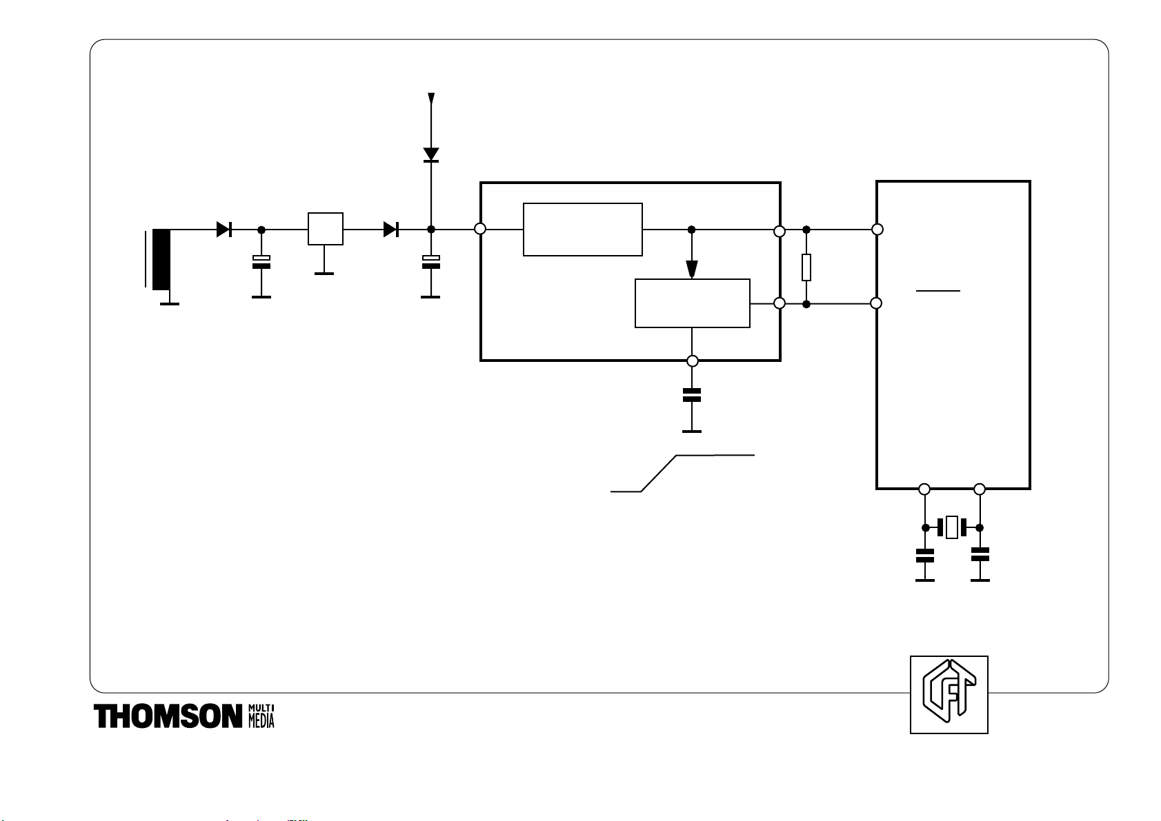
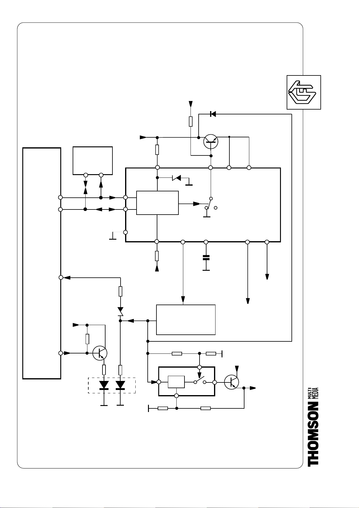
IR001 POWER SUPPLY AND OPERATIONAL SIGNALS
POWER SUPPLY
The power supply to the microcontroller at Pin 23 is active when the IP130
regulator (which produces a 10VSTBY) and the IP140 regulator (which
produces a 5VSTBY from the 10VSTBY) are on Standby. When they are On,
the 13 V (LINE) supply takes over from the 10VSTBY.
CLOCK.
A 27-MHz QR001 quartz stabilises the system clock of the IR001
microcontroller (Pins 46 and 48).
RESET.
CP142, Pin 3 of the IP140 is the Reset capacitor. When the voltage at Pin 9 of
7
the IP140 has reached 5 V, and after a delay of a few milliseconds given by
CP142, Pin 6 of the IP140 goes from 0 to 5 V. Pin 49 of IR001 receives this
Reset signal.
NOTES :
CENTRE DE
FORMATION TECHNIQUE
7
Page 11
RESET
+5VSTBY
RIR
STB-LED
CLAVIER
LDR
AFC
AV1
AV2
MUTE
MUTE C
SAT_ON_DEG
FB_DET
TV OFF
ZOOM
E-FIELD
I2C-1
I2C-2
SND-RESET
INT
BUS M3L
IR001
ST90R92
EEPROM
IR003
IR004
BE_STROB
EPROM
IR002
256 Ko
4 Ko
Expander
RAM
REGISTRES
TIMER
SAFETY
Bus µp
QR001
M-RESET
POWER-FAIL
Alim.
VIDEOTEXT
DEFLECTION
VIDEO MATRIX
PIP MODULE
DOLBY SOUND
TUNER CCT5000
CHROMA 1H / 2H
PSI 2H
MEGATEXT
VIDEO MODULE
100HZ
MODULE
27MHZ
MARK-E-TING
Data
Addresses
DS
46
48
23
51
53
43
42
44
45
62
52
54
27
40
41
49
55
28
63
64
65
25
39
29
33
32
31
34
VIDEO ADJUSTMENT
8
CENTRE DE
FORMATION TECHNIQUE
8
Page 12

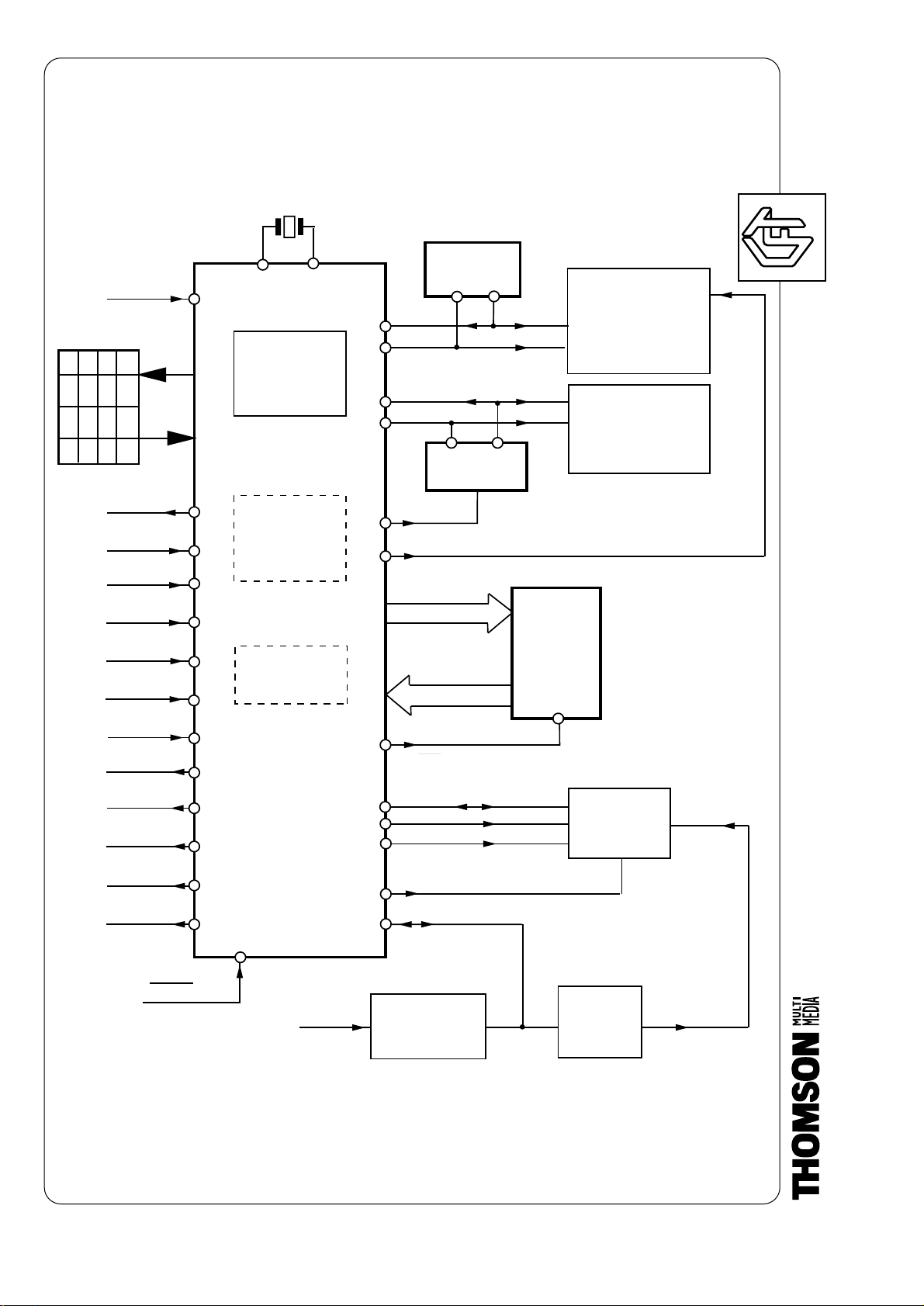
DATA MANAGEMENT
ICC19 chassis are 50-Hz or 100-Hz compatible. They are controlled by an 8bit microcontroller, the ST90R92.
It communicates via an address and data bus with its external program
memory, an EPROM, IR002, with a basic capacity of 256 KB that can be
extended to 1024 KB.
Two I2C buses dialog with the various programmable circuits installed on the
chassis.
In conjunction with IR003 (EEPROM), the I2C1 bus saves the parameters and
settings required by the television set.
It manages the ON/OFF command, the line and frame time base circuits, audio
and video switching, and settings including the USYST voltage.
9
In conjunction with the tuner frequency synthesis, the I2C2 bus controls video
processing and the 100-Hz digital converter.
It also controls an 8-bit IR004 universal register (EXP ANDER), which increases
the number of control ports.
NOTES :
The M3L bus is intended for the TELETEXT module (MEGATEXT version).
The microcontroller analyses and distributes the commands from peripheral
devices, the infrared receiver, the keypad, and the red LED via several input
and output lines.
The INT line is the HALT input of the microcontroller, and the MAIN RESET
output of the TELETEX module.
CENTRE DE
FORMATION TECHNIQUE
9
Page 13
A
B
C
D
58
59
60
53
VOL+
VOL-
PROG+
PROG-
INSTALL
EXIT
MENU
MUTE
INFO
RR
039
RR
040
RR
038
RR037
RR045
RR032
RR033
RR034
RR035
RR044
5VSTBY
5VSTBY
RIR
IR001
KEY OUT
KEY IN
RR924
OPTION
35
36
37
38
10
CENTRE DE
FORMATION TECHNIQUE
10
Page 14

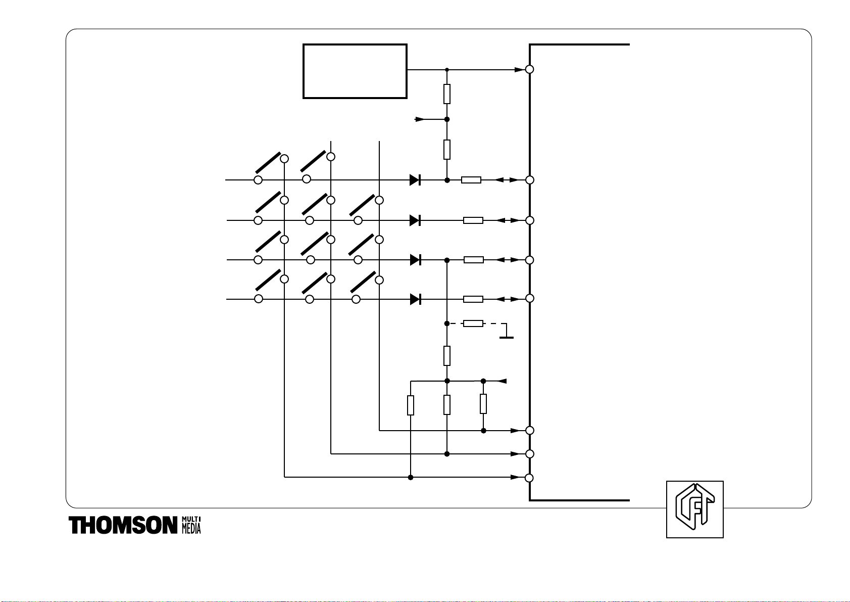
CONTROLS
KEYPAD
The keypad is compatible with previous ICC10/11 chassis. It can support four
to 10 control keys. It is laid out in a matrix of rows and columns.
Pins 58 through 60 are the function inputs. They are at 5 V when idle. Pins 35
through 38, which are labelled A, B, C, and D, are the sweep outputs. Signals
with a period of 20 ms are present on these outputs when idle.
During the initialisation phase, Line C (Pin 36) is connected to the input and
analysed. In this way , an option prediction, determined by Resistor RR924, can
be read.
The four diodes protect the IR001 circuit inputs.
REMOTE CONTROL UNIT
LRemote control function codes (12 bits) arrive at Pin 53 of IR001. They consist
11
of the following:
• Four address bits,
• One call bit,
• Seven function bits, defined by the key pressed.
These codes are repetitive at 80-ms intervals.
NOTES :
CENTRE DE
FORMATION TECHNIQUE
11
Page 15
BS05
BS04
BS01
BS00
15 bits
8 bits
A0 - A14
D0 à D715 à 22
25
24
Data strobe line DS
16
17 à 21
5VSTBY
1 - 32
14
13
3
2
30
31
57
56
1 à12
et
66 à 68
4 à 12
23
25 à 29
13 à15
IR002
EPROM
IR001
µ C
12
CENTRE DE
FORMATION TECHNIQUE
12
Page 16

REMOTE CONTROL UNIT
ADDRESSING
The IR002, memory for the software and default values, is an EPROM with
capacity up to 512 KB or 4 Mbits.
The 8-bit ST90R92 microcontroller has an address bus (A0-A14) limited to 15
bits. This provides addressing of only 32 KB. Page-swapping is therefore
necessary.
Four output port lines (BS00 through BS05) swap the read-only memory for a
selection of 16 pages compatible with the use of an 8-Mbit memory capacity,
i.e. 1024 KB.
DATA
13
Data comprising eight bits, labelled D0 through D7, are sent via the data bus.
To prevent any conflict of addresses with the microcontroller internal RAM, an
enable line, called data-strobe, is activated in the low state when the
microcontroller communicates with its ROM. The rest of the time, the IR002 is
in tri-state to free the data bus.
NOTES :
CENTRE DE
FORMATION TECHNIQUE
13
Page 17
IR004
REGISTER
MC14094
IR003
EEPROM
M24C32
DR104
9,1V
RR
010
RR
011
+5VSTBY 13V L
M3L-CK
M3L-DA
M3L-ENAB
63
64
65
32
31
34
33
29
BE-STROBE
2
SDA
SCL
SDA
SCL
RR055
RR056
+5V
+5VSTBY
RR052RR053
IR001
1
11
8
14
6
3
12
13
16
15
5V
BG_INFO
L1_INFO
I_INFO
IIC2
IIC1
DEGAUSS
NORM
TUNER
VIDEO MODULE
PERITEL
AUDIO
IV001
8
7
5
6
VIDEOTEXT
TR095
µc
PIP
MEGATEXT
RR
012
14
CENTRE DE
FORMATION TECHNIQUE
14
Page 18

BUSES
The IIC1 bus is charged by pull-up resistors connected to the +5VSTBY. It is
active in Standby and On Modes.
It dialogs with the IR003 NVM (M24C32) to store the user parameters.
It distributes its commands to the SCART switching circuits, the Audio Module,
and the sweep and video processor (IV001).
The IIC2 bus, referenced by pull-up resistors connected to the +5V, is active in
On Mode only.
It communicates directly with the PLL built into the tuner. It controls the Video
Module as well as the IR004 expander circuit.
The M3L bus is used in controlling the Teletext or Megatext Module.
BUS EXPANDER
15
Integrated Circuit IR004 (MC14094) is an 8-bit serial/parallel register that
extends the interface capacity of the microcontroller.
It is equipped with a de-serialiser register and an output register. Its BESTROBE (Pin 1) has the function of transferring a service byte to its outputs.
• Pin 6: NORM is used via Transistor TR095 by Integrated Circuit FI II050.
• Pin 11: DEGAUSS. According to chassis option, this output delivers a relay
command pulse to degauss the tube.
• Pin 12: I-INFO adjusts the video level to the I standard.
• Pin 13: L1-INFO is used for switching to Band 1 L'.
• Pin 14: BG-INFO is used to operate filters to reject the neighbouring channel
(31.9 MHz) and to reject FM sound intercarriers (5.5 MHz or 6.5 MHz).
NOTES :
CENTRE DE
FORMATION TECHNIQUE
15
Page 19
40
54
28
52
43
44
45
62
41
27
42
IR01
TV_OFF
RR910
TR102
RR103
MUTE CENTER
MARK_E_TING
MUTE
LDR
RR042
RR043
13V (L)
sensor
AV2 (8)
AV1 (8)
(A/D)
(A/D)
(A/D)
FB_DET
SAT_0N
AFC
DR091
(A/D)
ZOOM /E-FIELD
(PWM)
(A/D)
µC
SAFE
C MUTE
DR090
16
CENTRE DE
FORMATION TECHNIQUE
16
Page 20

OTHER CONTROLS
The function of Pin 27 is to switch the power supply separately from the satellite
tuner.
Pin 40 is used to switch off the television set using a control independent of the
buses. This is very useful in the event of the buses being blocked.
The breathing line is pulled down via Transistor TR102. In addition, this line is
analysed by software to indicate whether the TV is a 100-Hz or 50-Hz model.
This is indicated by RR910 (RR910 = 10K, 4 V at 40 = 100 Hz; RR910 = 0,
0.6 V at 40 = 50 Hz).
Pin 41 has two functions:
• To control the ZOOM Module if the television set is so equipped.
• On the 28" SF and 32" 16/9 modules, it delivers a PWM (pulse width
modulation) signal to compensate for the earth's magnetic field.
Pin 42 informs and analogue-to-digital converter for the AFC (automatic
17
frequency control). It operates in Automatic Programming and Manual Search
Modes.
Pin 43 informs an analogue-to-digital converter. This is used to regulate the
contrast according to the ambient lighting.
Pins 44 and 45 receive slow switching from SCART sockets AV1 and AV2.
They are used to recognise the formats of received images: 4/3 and 16/9.
NOTES
Pin 52 mutes the audio amplifiers. It is active at low level, and is present each
time the TV is switched on or off.
Pin 54 is reserved for the DOLBY SURROUND PROLOGIC function only, to
perform a software cut-off of the TV internal speakers, to free the central
channel. It does not act on the auxiliary external output sockets.
Pin 62 indicates the presence of fast switching from SCART socket AV1.
At Pin 28, the input when the microcontroller is initialised by its pull-up wiring
specifies the size of the read-only memory, IR002, by selecting the number of
pages to swap. It is completed by the wiring of Pins 63 and 61 to the 5VSBY.
CENTRE DE
FORMATION TECHNIQUE
17
Page 21
R
V
VCC1
RV001
TV002
RV002
20
24
44
22
M
V
19
18
65
31
32
IR003
24C32
IR001
REGISTER
INTERFACE BUS
65
M3-ENAB
DATA
CLK
43
I-CUT
38
17
37 25
CV246
DR104
9,1V
RR010
HORIZONTAL
DEFLECTION
TR002
RR031
RR036
RR29
51
REGULATION
CTL
VERTICAL
CTL
Cde
LIGNE
+5vSTBY
10VSTBY
+UVERT
8V
IV001
STV2161/
STV2162
ST90R92
13v
45
34
RV091
RR030
5V
REG.
RP148 RP149
RP142
RP143
TP146
+5V
5,8V
de DP140
2
4
8
7
IP140
DP134
18
CENTRE DE
FORMATION TECHNIQUE
18
Page 22

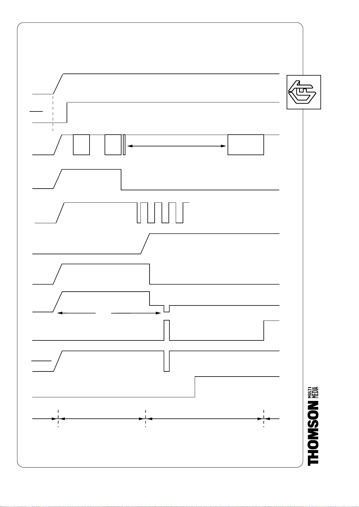
SWITCH-ON PROCEDURE
FRONT PANEL LED CONTROL
The 10VSTBY from the power supply is used. This is limited to 5 V by a Zener
diode inside the IV001, and powers its IIC1 bus interface.
After its power supply , clock, and reset, the IR001 microcontroller manages the
following commands:
• RAM reading,
• I/O configuration of ports,
• Reading EEPROM, IR003. To be programmed, if necessary, using the default
values contained in the IR002 program memory, if it is deprogrammed or
blank.
When an ON command is issued, the IR001 microcontroller initialises IV001
via its IIC1 bus with values stored in the EEPROM (loading of essential
parameters: on, geometry, etc.). Pin 24 on the IV001 is freed, and leads to the
presence of VCC1 = 8 V via TV002. This voltage powers Pins 22 and 44 of the
19
IV001.
The line time base, secondary regulation, and frame time base are gradually
powered up by the slow-starting capacitor, CV246 (Pin 17 of IV001).
The rising of the line 13 V transmitted by DR104 confirms that the On function
is fully established (5V at Pine 65 of IR001). This 13VL also makes it possible
to obtain a +5V via the IP140 regulator.
In Standby Mode, Pin 51 of microcontroller IR001 is in high impedance.
Switching transistor TR002 powers the red LED from the 5 V STBY.
In On Mode, the 13 V from the line time base powers the green LED. This is the
initialisation phase, and results in the indicator lamp glowing orange.
When the warm tube signal, sent by the I2C1 bus to IR001, is detected, Pin 51
of IR001 goes to 0. This blocks TR002 and cuts off the power supply to the red
LED.
The ICUT signal (Pin 43 of IV001) indicates when the tube is warmed up, and
frees the analogue controls. The image and sound appear. Orders routed in
from the outside, e.g. from the keypad or the remote control unit, are then
processed.
CENTRE DE
FORMATION TECHNIQUE
19
Page 23
20
Init.
IV001
40ms
10v STBY
5v STBY
400ms
Reset
IIC1
TV-OFF
H-DRIVE
+13v
+5V
IIC2
M3L
Interrupt
Power
fail
M-Reset
Mute C
Mute
I CUT
OFF to ON CHRONOGRAM
0V
+1,2V
100ms
RED ORANGE GREENOFF
1s
H
DRIVE
ON
4s
100ms
0,5ms
PB
NVM
CENTRE DE
FORMATION TECHNIQUE
20
Page 24
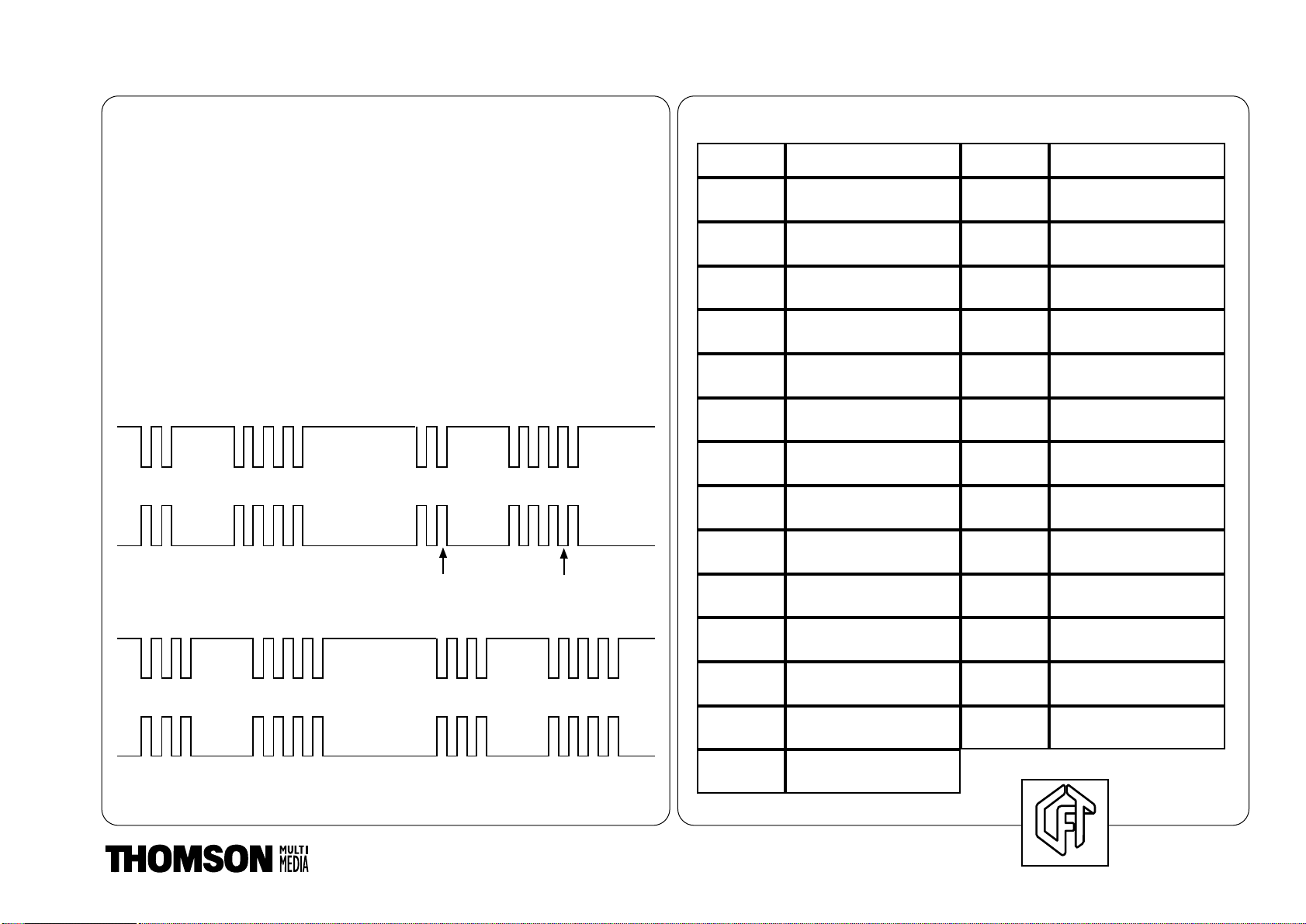
ERROR CODES
LIST OF ERROR CODES
These error codes are displayed by the red LED. They are displayed only if the
management microcontroller is operating.
A maximum of 81 codes (1 1 through 99) can be signalled. These codes consist
of two digits separated by a 0.7-second pause. The error codes are repeated
again and again, with a pause of 1.7 s between error codes.
SIGNAL RATE AT 2 OF BR001
There are four possible waveforms, according to whether the TV remains in
Standby Mode or is switched On, and whether LED pause status is Off, Red,
Orange, or Green.
pause
orange
21
0,7 sec. 1,7 sec.
24
0,7 sec.
0,7 sec.
1,7 sec.
pause
vert
250ms250ms
pause
rouge
1,7 sec.
34
0,7 sec. 1,7 sec.
pause
éteint
vert
orange
éteint
rouge
CODE
11
12
13
14
15
16
17
18
19
21
22
23
24
25
ERROR CODE
ACR MSP3410
ACR MSP3400
ACR DSP56004
ACR STV2161/2162
ACR STV2151ou
TDA9143
ACR DMU0
AUDIO MODULE NOT
DETECTED
ACR TEA6415C
ACR TUNER
IIC1 DATA EARTHED
IIC2 DATA EARTHED
IIC1 CLOCK EARTHED
IIC2 CLOCK EARTHED
SWITCHED 5 V ABSENT
26
27
28
29
31
32
33
34
35
36
37
38
39
ERROR
NO WARM TUBE SIGNAL
AFTER 15 s
STV216X DETECTED A CASE
OF PROTECTION 3 TIMES
MEGATEXT INTERFACE
NOT RESPONDING
MEGATEXT DRAM IS
DEFECTIVE
NO RAM AVAILABLE FOR THE
REQUESTED FUNCTION
TIMER OCCUPIED
ACR STV2165
ACR NVM M24C32
13V ABSENT
NVM ADDRESS NOT
FOUND
INCORRECT NMI LEVEL
(HALT)
M3L BUS IS BLOCKED
MEGATEXT NOT LISTENING
CENTRE DE
FORMATION TECHNIQUE
21
Page 25

22
CENTRE DE
FORMATION TECHNIQUE
22
Page 26

CONTENTS
INTRODUCTION
PRINCIPLE
CHARACTERISTICS
LP020 POWER SUPPLY
INTEGRATED CIRCUIT TEA2261
SECONDARY REGULATION
23
POWER SUPPLY
POWER SUPPLY INTERLOCKS
MAINS POWER CUT DETECTION
CENTRE DE
FORMATION TECHNIQUE
23
Page 27
24
+300V
TP060
220V
LP 070
LP020
14
Safety
2
9
IP060
TEA
2261
16
DP110
10
11
3
DP109
CP060
Usys
CP061
RP061
76
1
8
15
Logic
Processor
DP130
-US
Osc
PWM
Soft start
DP108
Power/
Deflection
safeties
RL81/82
RP054
CP
054
+US
+10V
STBY
GNDS
CP063
RP025
IP130
DP133
+13V
+U
VERT
RL80
+US
-US
+5V
IV001
(STV2161)
(STV2162)
SMPS
SMPS
CP020
Regulation/
Deflection
safeties
10V
Reg.
PFCPFC
(50Hz)
Contr.
(100Hz)
TP025
RP060
RP059
TP027
(Option)
RP065
RP020
CP062
CP064
DP053
DP050
DP
052
12
DP
134
TP161
DP140
IP140
5V
STBY
+5V
TDA8139
MIS
BREATHING
+U13
DP60
CENTRE DE
FORMATION TECHNIQUE
24
Page 28

25
INTRODUCTION
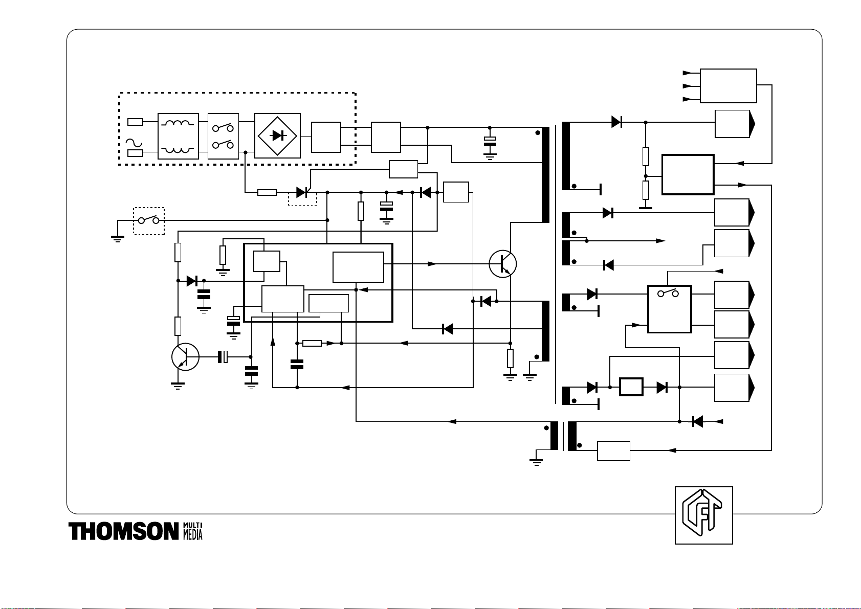
The ICC19 power supply comes in two main versions: one operating at 16
kHz, and the other operating at 32 kHz. The main difference lies in the choice
of components.
PRINCIPLE
IThe power supply is a fixed-frequency flyback-type switching power supply
unit. Two specific regulating loops come into action according to the status
of the TVC.
In Standby Mode, the frequency is determined by an oscillator located on the
primary.
This is also where regulation occurs. To do this, a signal indicating the
overall consumption of the secondaries, picked up on a primary winding, is
used.
In Steady-State Mode, the line frequency synchronises the signal.
Regulation then takes place at the secondary, and is based on stabilising the
voltage USYS applied to the line time base.
CHARACTERISTICS
TMains voltage: 190 to 264 volts.
Secondary voltages:
NOTES :
U SYS 127 to 136 V for 50-Hz chassis.
130 to 142 V for 100-Hz chassis.
+ US approx. +18 V for stereo chassis
approx. +14 V for Dolby chassis.
- US approx. -18 V for stereo chassis
approx. -14 V for Dolby chassis.
UVERT 26 V on 50-Hz chassis
23 V on 100-Hz chassis.
U 7V 6 to 7 V5 according to chassis.
CENTRE DE
FORMATION TECHNIQUE
25
Page 29
220VAC
Um
C1
b
Um
Im
a
-
R
+
C2
L1 D1
n
c
2n
Im
-
R
+
C
Uc
RL
220VAC
26
Um
Uc
Im
Narrow current pulse including
a high harmonic level
Um
Ub
ID1
Im
D1 conduction
level when
T1 is ON
Without PFC
With PFC
T1
Ua
Um
WITHOUT PFC CIRCUIT
WITH PFC CIRCUIT
CENTRE DE
FORMATION TECHNIQUE
26
Page 30

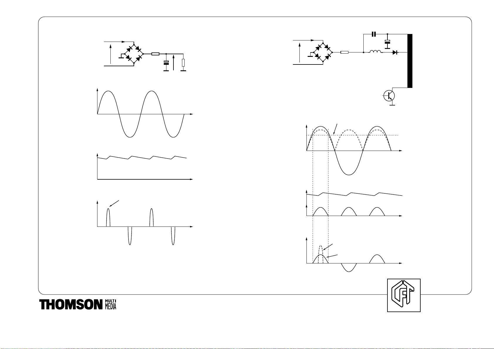
27
LP020 POWER SUPPLY
The new European standard, EN60555-2, limits pollution of the mains
voltage by harmonics. For this purpose, the main primary winding is
connected to the bridge rectifier via a power factor correction circuit.
PRINCIPLE
Harmonics are generated by the filter capacitor charging current.
The narrower the charge pulse, the higher the amplitude of the harmonics
(this occurs with a weak voltage residual and therefore a high capacitor
value).
The layout used for this chassis therefore operates on the principle of
widening these charging current pulses to reduce the amplitude of
harmonics. To do this, a condenser C1 is inserted between the diode bridge
and filter condenser C2 (C1 < < C2). It decouples the dc voltage between
Condenser C2, charged to 300 V, and the diode bridge, providing full-wave
rectification of the mains voltage.
An intermediate tap on the primary winding divides the winding so that when
Transistor T1 conducts, the voltage at Point C is about 2/3 the value of the
voltage at Point B. This, as soon as the rectified mains voltage exceeds this
value (Point A), Diode D1 conducts, and the current is tapped directly off the
diode bridge.
Because of this, a lower load is applied to Capacitor C2 (resulting in a lower
charging current), and the mains voltage takes effect over a longer period.
The current pulse taken from the mains therefore generates a lower level of
harmonics.
NOTES :
CENTRE DE
FORMATION TECHNIQUE
27
Page 31

DP018
DP10
DP12
DP13
DP11
DP16
DP019
CP11
4n7
CP12
4n7
CP15
470n
CP13
CP018
1µ
CP017
470p
CP020
CP019
470p
LP019LP15
RP10
2R7
MIS
CHASSIS
TP060
3/4
1/2
5/6
n
2n
28
CENTRE DE
FORMATION TECHNIQUE
28
Page 32

29
APPLICATION
A filter, CP15, CP018, and LP15, eliminates the mains pollution generated by
the line frequency switching of Diode DP019 (D1).
Diode DP16 protects CP15 (C1) against voltage spikes on the mains.
Diode DP018 limits the collector overvoltage of TP060 (T1) when diode
DP019 is blocked.
NOTES :
CENTRE DE
FORMATION TECHNIQUE
29
Page 33

+
-
+
-
+
-
GENERATOR
"BURST"
SOFT
START
STBY
OSC.
IS
SOFT
+-
STBY
STARTING
TA
SOFTWARE
CONTROL
TB
REGULATION
ORDER
4,5 µA
10 µA
+
-
0,15 V
+
-
+-
POSITIVE
SW
NEGATIVE
SW
TC
0,9 V
0,6 V
2,6 V
OVER VOLTAGE
PROTECTION
LIMITATION
I
INNER
POLARISATION
INNER
REF.
2,5 V
SAFETY
Vcc
+
-
15,7 V
OVER
VOLTAGE
9
11 10
12 8 3 4
13
5
12
GND
6
AMPLIFIER
ERROR
1
2
β
α
3
7
16
Vcc
15
V +
14
2,5v
30
CENTRE DE
FORMATION TECHNIQUE
30
Page 34

31
INTEGRATED CIRCUIT TEA2261
TEA2261 incorporates the various stages required for control and regulation
of a switching power supply unit. It includes the following:
Internal voltage reference and regulation circuit
Error oscillator
Error amplifier
Pulse width modulator (PWM)
Gradual start circuit
Transformer degaussing control
Current limiting threshold detection
Logic management of limits and interlocks
Output stage for direct drive of a bipolar power transistor.
Because of the automatic switching of SALVES Mode in the event of low
consumption, this circuit handles a wide range of regulation tasks, from a few
watts to values in the region of 200 W.
NOTES :
CENTRE DE
FORMATION TECHNIQUE
31
Page 35

32
12V
IP050
RECTIFIER
PFC
FILTER
220VAC
300VDC
LP020
3/4
8
10
9
RP050
10R
DP052
DP053
DP051
CP054
470µ
CP054
470µ
RP030
à
RP032
360k
RP025
33k
CP020
RP029
100k
RP055
15R
CP055
4n7
CP056
47µ
DP050
TP060
CP052
10µ
14
7809
16
+
-
+ Vcc
REF.
2,5 V
15,7 V
I
SIGNAL
RESET
Vcc < 5V5
REGUL.
Vcc INT.
5 V
R1
R2
PROTECTION
OVER VOLTAGE
Vcc
Vcc MAX.
RESET
Safety
V REF.
2,5 V
Vcc OFF
Vcc INT.
5 V
10v3
7v4
15
Output
power
supply
IP060
TEA2261
RP054
CENTRE DE
FORMATION TECHNIQUE
32
Page 36

33
GENERATION OF INTERNAL REFERENCES AND POWER SUPPLIES
The power supply at Pin 16 comes from:
On start-up, half-wave rectification of the mains by the mesh RP025, CP054,
and a diode of the bridge rectifier.
In Standby Mode, winding 9, 8 of LP020 (fly-back mode). 12 V obtained by
rectification (DP050, CP054) is applied to regulator IP050 (7809 applied to
Diode DP051), which supplies 9 V via DP052.
In Steady-State, winding 9, 10 of LP020 (fly-back mode). Rectification by
DP053 supplies a voltage of about 11 V.
Note that in this case Diode DP052 is blocked, and disconnects circuit IP02.
Resistor RP054 delivers the power supply to the final stage (Pin 15), and sets
its maximum current.
The circuit supplies several voltages and service signals according to
changes in the direct current voltage at Pin 16.
As soon as +Vdc reaches approximately 4V5, an internal reference of +2V5
is generated.
For +Vdc £ 5V5, a RESET pulse is produced.
NOTES :
When +Vdc reaches 10V3 (Vdc start), enabling of an internal power supply
Vdc int = 5 V. This stabilised voltage allows the circuit to perform well in a
wide voltage range on Pin 16.
This threshold also triggers the passage to high state of Vdc off, thus
enabling the interlock and limit management logic, and authorising pulse
output from Pin 14 (as long as +Vdc remains higher than +Vdc stop, i.e. 7V4
typ.).
For Vdc of 15V7 typ., passage to high state of Vdc max, and interlocking of
the circuit by the interlock and limit management logic.
CENTRE DE
FORMATION TECHNIQUE
33
Page 37

34
220VAC
CP055
4n7
RP025
33k
TP025
DP027
CP056
47µ
TEA2261
16
IP060
RECTIFIER
FILTER
RP055
15R
PFC
RP028
100k
DP034
DP028
5V1
14
RP030
à
RP032
360k
RP029
100k
300VDC
TP026
RP026
100k
DP052
CP052
10µ
DP053
CP054
470µ
TP060
CP020
RP027
DP051
10k
IP050
12V
7809
DP050
CP054
470µ
3/4
RP050
10R
10
9
LP020
8
RP055
15R
CP055
4n7
220VAC
RP035DP035
CP056
47µ
RP025
33k
TEA2261
16
IP060
RECTIFIER
FILTER
DP054
PFC
14
RP030
à
RP032
360k
RP029
100k
300VDC
DP052
CP052
10µ
DP053
CP054
470µ
TP060
CP020
DP051
IP050
12V
7809
POWER STANBY SWITCHING
LOW POWER SWITCHING
FORMATION TECHNIQUE
CENTRE DE
34
Page 38

OPTIONS
SWITCHING OF START-UP POWER SUPPLY
On 100-Hz chassis, a thyristor (TP025) is added in series with Resistor
RP025.
When mains power is applied, a current from the 300 V via the RP028,
RP030 through 32 resistor network energises the thyristor. The thyristor then
channels the CP054 charging current.
When the power supply starts up, a voltage of 9V6 appears at the output of
Regulator IP050 and saturates Transistor TP026. With its gate then earthed,
the thyristor de-energises the next time the mains alternation is inverted.
This layout reduces the consumption by 0.7 W.
NOTES :
35
LOW-POWER SWITCH
A low-power switch can be connected in series with Resistor RP025 to
replace the classic mains switch.
In operation, this switch connects RP025 via Resistor RP55 to Pin 16 of IP60.
In Off position, this switch switches Pin 16 of IP060 to earth via Resistor
RP035 and Diode DP035.
Zener Diode DP054 limits the voltage to the terminals of CP54 when Off.
CENTRE DE
FORMATION TECHNIQUE
35
Page 39

V REF+Vbe
Q2
Q1
RP061
270k
11
CP060
1n
10
THRESHOLD
COMPARATOR
2 K
Q3
R1
R2
R3
3V33
1V66
LP020
8
10
DP050
RP050
10R
CP051
100µF
RP059
47k
Q1'
DP060
IP050
DP051
CP052
10µ
7809
R4
CP063
4n7
8
RP060
270k
Safety
CP062
10µ
RP062
1M
TP027
Primary
regulation
Self
power supply
IP060
TEA2261
36
CENTRE DE
FORMATION TECHNIQUE
36
Page 40

OSCILLATOR
An oscillator determines the switching frequency of the switching device in
Standby Mode.
It includes the following:
- Current (Q1, Q1', Q2) generator; value of current set by Resistor RP061
(Pin 11).
This current charges Capacitor CP060 (Pin 10).
Threshold detector which analyses the voltage across CP060:
• 1st threshold (2/3 Vdc int. = 3V33 typ.): switching of transistor Q3 and
discharge of CP060 by internal 2 kW resistor.
• 2nd threshold (1/3 Vdc int. = 1V66 typ.): blocking of transistor Q3 and
charging of CP060 by the current generator.
NOTES :
37
The overall result is a sawtooth.
Function of components RP059, RP060, and DP060.
In the start-up phase, because the secondary voltages are low, the time
required to restore the energy is liable to exceed the nominal period of the
oscillator. The oscillator therefore starts up with a low frequency (approx. 5
kHz) due to components RP061 and CP060 only (Diode DP060 is blocked).
With the increase in voltage at the IP050 output, Diode DP060 begins to
conduct, and the current determined by RP060 gradually contributes to an
acceleration of the charging of CP060, thus bringing the oscillator frequency
up to 19 or 20 kHz.
Resistor RP059 is connected to earth via the conduction of transistor TP027,
and contributes to reducing the charging current of Capacitor CP060 and
therefore the frequency of the oscillator in the event of the primary interlock
being triggered (refer to paragraph on interlocks).
CENTRE DE
FORMATION TECHNIQUE
37
Page 41

Threshold
1v5
180µA
9µA
9
+
-
+
PULSES
GENERATOR
1
β
2
CP061
470n
U err
OSC
PWM
U int
α
LP020
6
-
+
ERROR
AMPLIFIER
7
V REF.
2,5V
9
RP066
4k22
RP064
1k
V REF. :
2,5 x 0,9 =
2,25 V
SPECIAL
SOFT
1 ; 0,9
14
TA
IS
Output
Safeties
300V
T onmin
(1µs)
OSC.
TP060
8
DP050
RP050
10R
CP051
100µF
IP050
DP051
7809
CP064
22n
Standby
self power supply
DP061
15
Output
power supply
Safeties
3
Info.
I TP060
RP065
38
CENTRE DE
FORMATION TECHNIQUE
38
Page 42

PRIMARY REGULATION LOOP
This includes an error amplifier that compares a fraction of the image of the
secondaries (Winding 8, 9, RP050, DP050, CP051, RP066, RP064) to an
internal reference.
Resistor RP065 sensitises the primary circuit in Standby Mode.
In Steady State, because the secondary regulations brings the voltage at
Pin 6 to approximately 4V7, the primary regulation is in a constant
overvoltage configuration, and automatically shuts itself off.
A first PWM then compares the error voltage to the sawtooth signal from the
oscillator, to produce a command strobe pulse (signal a).
A second PWM defines the maximum authorised duty cycle (60%) by
comparing the same sawtooth signal to an internal voltage (signal b).
A logical AND operator between these two signals produces the narrowest
strobe pulse.
NOTES :
39
When switching on, and at the beginning of each burst, a soft start is ensured
by controlling the internal voltage and therefore the width of signal b: from
T1 to T2, Capacitor CP061 (Pin 9) is charged by an internal generator
producing a current of 180 µA. There is no signal at the IC output.
At T2, the voltage at the terminals of CP061 reaches 1V5. The charging
current goes to 9 µA. Strobe pulses appear at Pin 14, corresponding to
signal b which is widening (Tb < Ta).
A few milliseconds after T2, the soft start circuit stops limiting strobe pulse
width, and the primary regulation loop becomes established (Ta < Tb).
When the voltage reaches 2V7 typical, it sets the maximum duty cycle
(b = 60%).
The load on CP061 (maximum value 3V1) is returned to 800 mV at the end
of start-up and at the end of each burst.
CENTRE DE
FORMATION TECHNIQUE
39
Page 43

IP060
TEA2261
2
LP070
RP068
1k
Primary
regulator
Soft
Vcc int.
Secondary
regulator
-
+
0V9
-
+
150mV
Vcc ext.
1
500R
RP050
10R
RP069
22k
DP050
LP020
CP068
470p
8
40
CENTRE DE
FORMATION TECHNIQUE
40
Page 44

41
LOGICAL IS STAGE.
During the transition between Standby and Steady State, the two regulation
loops coexist. Because the signals are not synchronous, there is a risk of a
Transistor TP060 command during the energy restoration phase, and of the
interlock being triggered by a current peak.
To avoid this problem, a signal taken from Winding 8, 9 and applied to Pin 1
warns the circuit of this critical phase. All commands are then blocked.
The first negative front (corresponding to the end of energy restoration =
transformer degaussing) enables any new primary or secondary commands.
NOTES :
CENTRE DE
FORMATION TECHNIQUE
41
Page 45

42
-
+
-
+
+
Tc
_
Q
R
S
2v6
CP063
4n7
8
45 µA
10µA
Q1
_
Q1
S
R
B1
_
Q2
Q2
B2
S
R
Vcc
off
Tb
1st level
2nd level
0V6
0V9
15V7
Vref
2V5
(10V3, 7V4)
5V int
3
16
RP020
0R1
TP060
Vcc Max
RESET
-
+
CP062
10µ
RP062
1M
RP059
47k
RP060
270k
RP067
1k
RP063
7
RP065
-
+
6
14
RESET
Vcc < 5V5
+Vcc
CP056
47µ
LP020
RP025
33k
220V
RP055
15R
8
DP050
IP050
DP053
7809
TP027
10
DP052
CP054
470µ
OSC
CP060
1n
10
DP060
Primary
regulation
RP066
CENTRE DE
FORMATION TECHNIQUE
42
Page 46

43
AINTERLOCK ACTIVATION AND MANAGEMENT
The TEA2261 has a strobed current interlock at Pin 3 and an interlock related
to the power supply voltage at Pin 16.
An image of the current is collected at the terminals of emitter resistor RP020,
and applied to Pin 3 of TEA2261. The following two thresholds apply:
1ST THRESHOLD INTERLOCK
When the voltage at Pin 3 reaches the first threshold, 0.6 V , TP060 is blocked
until the next Tb pulse (bit-by-bit limitation). During this time, CP063 is
charged by a current of 45 - 10 = 35 µA.
When this phenomenon is repetitive, the charge on CP063 reached 2V6 and
triggers an RS-bistable circuit which permanently disables control of TP060.
A main reset is then necessary to re-start the circuit (Vdc 5V5).
2ND THRESHOLD INTERLOCK
In the event of a major overload (short circuit on USYS), a second threshold
is reached (0V9). Control of TP060 is permanently disabled. A main reset is
then necessary to re-start the circuit (V Pin 16 5V5).
VOLTAGE INTERLOCK
A voltage above 15V7 on Pin 16 blocks TP060. A main reset is then
necessary to re-start the circuit (V Pin 16 5V5).
SPECIFIC FEATURES OF ICC19 CHASSIS
NOTES :
Because the primary interlock is calibrated for U SYS at steady state, the
sensitivity of this stage has been increased in Standby Mode to detect faults
on the other secondaries.
For this purpose, a resistor, RP065, is added between the error amplifier
output of the primary loop (Pin 7 of IP060) and the interlock input (Pin 3).
When capacitor CP063 reaches 0.6 V, Transistor TP027 conducts and
reduces the charging current of Capacitor CP060 (RP059), which reduces
the frequency of the Standby oscillator.
CENTRE DE
FORMATION TECHNIQUE
43
Page 47

RP54
RP028
RP030 à 32
460k
RP029
100k
CP022
470p
CP023
2n2
DP022
FUF
4005
3/4
RP022
100R
5/6
LP020
CP112
RP112
1k2
18
LP
112
DP110
DP112
MUR
1100E
DP113
+
USYS
CP110
100µ
44
IP060
TEA2261
15
14
12/
13
LP040
RP040
22R
DP040
2V7
CP040
470µ
CP041
1n
RP042
4k7
DP041
BAT42
RP041
47R
TP060
LP042
CP042
1n
RP050
0R10
CP021
150p
CENTRE DE
FORMATION TECHNIQUE
44
Page 48

TP060 ENVIRONMENT
OUTPUT STAGE
The output stage of the TEA2261 consists of a push-pull.
It supplies the basic current for control of TP060, and then channels the
reverse locking current caused by the discharging of CP040.
In the conduction phase, Resistor RP054 limits the polarisation current.
TP060 SWITCHING CIRCUITS
Resistors RP029 through RP032 pre-charge CP040 as soon as power is
switched on, to ensure an adequate reverse locking current during the startup phase and at the beginning of each burst. Self-induction coil LP040 sets
the dl/dt of the control current reversal.
NOTES :
45
The circuit DP022, CP023, RP022 slows the rise in collector voltage of
TP060 when it is blocked, to ensure minimum dissipation through switching,
and to limit the overvoltage peak. To do this, it is assisted by the secondary
assembly DP113, LP112, RP112, CP112, and DP112.
CENTRE DE
FORMATION TECHNIQUE
45
Page 49

46
LP020
16
13
17
18
15
14
12
18
DP140
DP130
DP110
DP108
DP109
+U7V
IP130
1
7812
2
GNDS
IP140
TDA8139
DP133
3
DP
134
Usys
+US
-US
+U13
+5V
5V
STBY
+U
VERT
+10V
STBY
+13V
Voltage
+USYS
+UVERT
+US
-US
+U7V
+USYS
+UVERT
+US
-US
+U7V
+USYS
+UVERT
+US
-US
+U7V
+USYS
+UVERT
+US
-US
+U7V
Black screen
sound mute
131,3V
26,1V
18,4V
-18,1V
7,7V
137,3V
26,0V
14,1V
-14,0V
7,52V
134,2V
22,7V
18,6V
-18,4V
5,95V
134,2V
23,5V
13,5V
-13,6V
6,05V
White screen
maxi. sound
50Hz stéréo
131,2V
26,5V
16,8V
-15,1V
7,87V
50Hz dolby
137,2V
26,3V
12,7V
-12,8V
7,68V
100Hz stéréo
133,9V
22,8V
15,2V
-15,2V
5,8V
100Hz dolby
133,9V
23,4V
11,1V
-11,5V
5,78V
Standby
190V
85,3V
15,1V
10,5V
-10,3V
6,7V
91,6V
14,9V
7,7V
-7,6V
8,5V
108,2V
13,9V
11,1V
-11,0V
6,8V
104,4V
13,9V
8,9V
-9,0V
7,2V
Standby
230V
86,7V
15,0V
10,6V
-10,3V
6,9V
91,3V
14,8V
7,7V
-7,6V
8,5V
109,6V
14,0V
11,3V
-11,1V
6,8V
105,9V
14,0V
9,0V
-9,1V
7,2V
CENTRE DE
FORMATION TECHNIQUE
46
Page 50

SECONDARY VOLTAGES
The secondary windings produce five direct voltages:
+USYS which can be between 127 and 140 volts, according to chassis, and
according to the winding connector selected (19 through 22 via jumpers
JP914 through 917).
+US and -US, symmetric power supplies with specific earth distributed to the
audio stage via a cable (from BP120).
+UVERT, vertical stage power supply voltage. Also applied to the regulator
circuit, IP30, and causes the polarisation of the base of TV002 (IV001 power
supply).
+U7V, voltage supplying the switched 5 V.
In Standby Mode, the 10VSTBY is produced by Regulator IP130 and Diode
DP133. In Steady State, the 13 V from the EHT takes over via Diode DP134.
NOTES :
47
The switched 5 V is obtained at Pin 8 of IP140 (switched by voltage +U13,
Pin 4) on 50-Hz stereo chassis, while a transistor, TP146, handles this
regulation task for 50-Hz Dolby and 100-Hz chassis (see illustrations below).
CENTRE DE
FORMATION TECHNIQUE
47
Page 51

VOLTAGES ELABORATION + 5 VSTBY AND + 5 V (50 Hz Stéréo VERSION)
LP020
CP143
470µF
DP130
DP134
DL041
DP133
IP130
IP140
TDA8139
DP140
CP130
2200µF
CP131
10µF
CP141
2,2µF
1
2
9
7
8
4
VI1
VI2
VO1
VO2
5V
Reg
Prog.
Dis
12V
RP148
18 k
RP149
4k7
CP144
10µF
RP143
2k32
RP142
2k21
CL045
470µF
CL042
1000µF
LL045
LL008
(THT)
10
12
RL040
0R27
ZL041
CP140
4700µF
JP911JP910
12
13
17
18
+ 5 V
STBY
+ 5 V
10 V
STBY
+ 13V
+U13
+U
VERT
48
CENTRE DE
FORMATION TECHNIQUE
48
Page 52

LP020
CP143
470µF
DL041
IP140
TDA8139
DP140
2
7
8
4
VI2
VO2
Reg
Prog.
Dis
RP148
18 k
RP149
4k7
RP143
2k32
RP142
2k21
CL045
470µF
CL042
1000µF
LL045
LL008
(THT)
10
12
RL040
0R27
ZL041
CP140
4700µF
CP146
10µF
TP146
VOLTAGE ELABORATION + 5 V (50 Hz Dolby / 100 Hz VERSION)
+ 5 V
+ 13V
+U13
49
CENTRE DE
FORMATION TECHNIQUE
49
Page 53

50
+10V
STBY
IP060
TEA2261
2
14
U SYS
300V
3/4
5/6
LP020
TP060
19/20/21/22
18
DP110
CP110
RL081/82
RL080
TP161
LP070
RV241
4k7
RP160
2k2
IV001
STV2161/2162
37
31
VCC1
IR001
ST90R92
VCC1
RP162
2k2
RP068
1k
RP138
10k
RP139
82k
RV242
1k
CV243
470p
CV242
470n
CV241
100p
RP161
330R
SMPS
CV246
220n
18/
19
//
31/32
17
CSOFT
SMPS IN
Régulation
Sécurité
BREATHING
22
28
33
RV213
(CL030/038)
DP160
RP163
2k2
Sécurités
Alimentation
Bases de temps
H REF
I2C1
13
DP140
TP162
fl
CENTRE DE
FORMATION TECHNIQUE
50
Page 54

51
SECONDARY REGULATION
This mode is adopted as soon as Steady-State Mode begins. It regulates
voltage USYS.
A fraction of USYS, tapped off by divider bridge RL082, RL081, and RL080,
is applied to Pin 31 of IV001 (SMPS IN).
This information is compared to an internal reference whose value can be
adjusted according to operating mode (USYS adjusted in 64 steps within a
16-V range).
A strobe signal at line frequency with a variable duty cycle is available on
Pin 37 (SMPS OUT).
This signal is applied to galvanic isolating transformer LP070 via Transistor
TP161.
A soft start circuit is associated with the production of the command strobe
signal. (CV246, Pin 17; when power is applied to circuit IV001, it is charged
to 5V5 in 900 ms.
The network RV242, CV242, CV243 limits the pass band of the entire
regulating loop to 300 Hz.
On 100-Hz chassis, Transistor TP162 controls transformer degaussing.
In the event of irregularities on the secondaries or in the time bases,
the interlock circuit forces the BREATHING line to low state (Pin 28 of IV001).
The regulating and time base commands are then stopped. If the error
persists after two more start-up attempts by IV001, the TV goes into Standby
Mode.
NOTES :
CENTRE DE
FORMATION TECHNIQUE
51
Page 55

LP40
DP40
CP40
DP133
IP130
12V
VCC1
IP140
Deflection
safeties
SAFE
TP060
LP060 DP110
DP109
DP140
DP130
USYS
TP129
TP190
TP175
TP170
TV002
TP161
VCC1
+ 5V
+U13
+U
VERT
+U
VERT
+10V
STBY
+5V
STBY
+US
-US
IP060
14
2
6
37
LP070
RP068
RP066
RP064
RP067RP065
RP063
DP050
RP050
10R
+10V
STBY
DP108
RP172
10k
RP191
4k7
RP192
100k
RP190
5k6
DP178
DP190
DP179
RP177
RP176
4k7
IV001
RP171
22k
RP193
4k7
RP170
10k
RP175
1K
CP171
22µ
RP129
10k
RP127
100k
RP128
2k2
RP130
0R10
CP126
100µ
RP126
2k2
DP
126
JL004
100R
RP179
22k
CP179
47µ
DP175
3
2
1
IR001
TR102
RR910
RR103
1k
RV
003
RV001
RP160
RP162
40
28
12/22/442324
37
SMPS
OUT
28
4
RP149
RP148
RP161
TV_OFF
CP170
4n7
52
CENTRE DE
FORMATION TECHNIQUE
52
Page 56

53
POWER SUPPLY INTERLOCKS
Overloads and short circuits are detected by analysing the primary current in
the emitter resistor of TP060 (input at Pin 3 of circuit IP060).
The sensitivity of this stage was increased in Standby Mode to detect errors in
the low-voltage secondaries (RP065, TP027, and RP059). For this reason,
when an incident occurs in Steady State on a secondary other than U SYS, it
is necessary to go to Standby Mode to trigger the interlock.
- An overload or short circuit on voltages +U VERT or +10 V STBY leads to
power supply VCC1 of the regulation and sweep circuit (IV001) disappearing.
- An overload or short circuit on +US causes TP190 and TP170 to conduct.
This forces the breathing interlock input of the regulation and sweep circuit
(IV001) to be triggered by a low level.
- An overload or short circuit on -US causes DP190 and TP170 to conduct,
and triggers the IV001 interlock.
In the event that external speakers with too low an impedance value are
connected (Dolby versions), or when incidents occur on the +5 V, simply shut
off the sweep to remove the overload:
- Excessive current in Resistor RP130 causes TP129 and TP170 to conduct,
and triggers the IV001 interlock (audio mute).
- A short circuit on the +5 V blocks TP175 through the action of DP178, and
causes TP170 to conduct (see sweep interlocks), causing the IV001 interlock
to trigger and the +13 V to disappear.
NOTES :
CENTRE DE
FORMATION TECHNIQUE
53
Page 57

DP
151
DP134
DP133
IP130
CP130
2200µF
CP131
10µF
CP141
2,2mF
19
5V
12V
CP144
10µF
17
18
+U
VERT
IP140
TDA8139
+U13
10 V
STBY
+ 5 V
STBY
+ 5 V
STBY
DP
152
RP156
1k
RP157
RP158
68k
CP151
220n
CP152
220n
RP159
330k
RP150
10k
RP151
12k
RP152
2k2
RP165
120k
RP164
100k
RP167
10k
RP145
10k
DP130
TP145
TP167
TR105
TR106
TP166
TP150
TP152
TR091
RP166
1k
RP144
1k
RR107
1k8
RR106
470
RP144
1k8
RR098
22k
RR099
10k
RR084
1k
RR085
100R
RR089
100R
RR091
4k7
POWER_FAIL
RR093
4k7
CR085
10n
DR
090
DR091
55 54 52
IR001
CP150
22n
CR092
100p
INT
MUTEMUTE C
M RESET
MUTE
C MUTE
54
CENTRE DE
FORMATION TECHNIQUE
54
Page 58

55
DETECTION OF MAINS POWER FAILURE
In the event of mains power failure, the microcontroller must be informed
promptly so that the data in the NVM (IR003) can be saved, and to avoid a
plop in the speakers (sound mute).
To do this, POWER FAIL has a rising edge in the event of mains power failure
in ON Mode, and a falling edge in the event of mains power failure in Standby
Mode.
The signal is received by the management circuit via the INTERRUPTION
input at Pin 55. Transistor TR091 produces a low mute level when the
phenomenon occurs in ON Mode.
The negative voltage rectified in Forward Mode by Diodes DP151/152 is an
image of the mains voltage. It blocks TP152 in ON Mode. TP150 and TP145
are blocked. TP167 is saturated, and the POWER FAIL line has a low level.
When the mains falls below 160 Vac, TP152, TP150, and TP145 conduct,
TP167 generates a rising edge on the POWER FAIL line by blocking off.
In Standby Mode, because voltage +UVERT goes from 23-26 V to 14 V, the
RP150/151 network saturates TP150, TP145 conducts and blocks TP167,
and the POWER FAIL line has a high level.
When mains power breaks down, the decrease in 10VSTBY saturates TP166
and TP167, and the POWER FAIL line has a falling edge.
NOTES :
CENTRE DE
FORMATION TECHNIQUE
55
Page 59

56
CENTRE DE
FORMATION TECHNIQUE
56
Page 60

CONTENTS
INTRODUCTION
PRODUCTION OF H-DRIVE COMMAND IN STV2161
SPECIFIC FEATURES OF STV2162
DRIVER STAGE
EHT AND LINE POWER
EW STAGE
57
TIME BASES
FRAME SWEEP
TIME BASE INTERLOCKS
CENTRE DE
FORMATION TECHNIQUE
57
Page 61

Regulator
HVCO
2MHz
Horiz. PLL
Horiz.
soft
Ph.1
Separator
Synchro
Ph.2
Alignement
Driver
LL008
SAFETY
Breathing
+10V
STBY
RL001
3k3
VCC1
RV222
680k
+10V
STBY
Soft
start
Frame
+ U
VERT
SSC
35
V BLK
HFLY
BLK
BG
Multiplexer
control
36
SMPS
I2C
IX900
TEA
6415C
15
RX950
RX951
TX950
Chroma
Module
RV202
150R
RV203
150R
CV201
680n
RV201
180R
16
TV002
TIP122
RV001
110k
24 22 23 44/12
RV003
24k9
21
CV207
4n7
CV206
1µ
CV246
220n
CV213
47p
CL211
470p
CL039
27n
CL038
27n
CL030
1n9
CV216
470p
CV222
22n
RV216
330R
JL004
100R
RV213
4k7
RL214
2k7
RV206
18k
TP170
TL062
Power
supply
and
deflection
safeties
ON/
OFF
18 19 33 17
H FLY
38
28
TL030
V SYNC
IV01
+13V
LI
DL134
STV2161
58
CENTRE DE
FORMATION TECHNIQUE
58
Page 62

INTRODUCTION
Time base commands are produced by the IV001 video processor:
STV2161 for the 50-Hz chassis.
STV2162 for the 1006Hz chassis.
Apart from the difference in frequency, the difference between these two
circuits is in the internal oscillator, which is used constantly in the STV2161,
but only for start-up in the STV2162 (an external 27-MHz signal then takes
over).
In Standby Mode, only the I2C interface of IV001 is powered. This allows the
microcontroller to manage start-up by freeing the transistor regulating control
TV002 (Pin 24), which then supplies the main power supply voltage to the
VCC1 circuit.
PRODUCTION OF H-DRIVE COMMAND IN STV2161
NOTES :
59
A VCO (sawtooth signal generator) operates at 2 MHz. It calls on a reference
current supplied by Resistor RV003 (Pin 23). Its free frequency can be
adjusted in 125-Hz steps in the 15,500-15,750 Hz range according to
operating mode.
The video signal is applied to the synchronisation separation stage by Pin 16
(SYNC-IN).
The resulting signal is brought to the first phase detector which generates an
error voltage on filter RV206, CV206, CV207 (Pin 21).
A HORIZONTAL-LOGIC stage then divides the frequency from the
automatically controlled VCO to apply it to the second phase detector.
The second phase detector also receives the HFLY line return (Pin 33). This
is where the horizontal phase adjustment takes effect; this also takes place
via Operating Mode.
A signal shaping stage increases the H-DRIVE signal on the open-collector
output (Pin 38). On start-up, this signal appears with a duration of 5 µs typ.
(low level), and then widens to 38 µs as the charging of CV246 progresses
(related to the soft start, Pin 17).
CENTRE DE
FORMATION TECHNIQUE
59
Page 63

Regulator
Ph.2
Alignement
Driver
LL008
SAFETY
Breathing
+10V
STBY
RL001
3k3
VCC1
RV222
680k
+10V
STBY
Soft
start
Trame
+ U
VERT
SSC
35
V BLK
HFLY
BLK
BG
Multiplexer
control
36
SMPS
I2C
6
TV002
TIP122
RV001
110k
24 22 23 44/12
RV003
24k9
21
CV207
220p
CV206
220n
CV246
220n
CV213
47p
CL211
470p
CL039
27n
CL038
27n
CL030
1n9
CV216
470p
CV222
22n
RV216
330R
JL004
100R
RV213
4k7
RL214
2k7
RV206
270k
TP170
TL062
Power
supply
and
deflection
safeties
ON/
OFF
18 19 33 17
H FLY
38
28
TL030
V SYNC
8
7
SLPF
Start
oscillator
HDFL
VDFL
LDFL
Frame
BV011
10
8
9
Up
Convertor
CV247
220p
13
Horizontal
counter
IV01
+13V
LI
DL134
STV 2162
60
CENTRE DE
FORMATION TECHNIQUE
60
Page 64

61
SPECIFIC FEATURES OF STV2162
For the STV2162, the separation of synchronisation pulses has already been
performed by circuit TDA9143 of the video module (50/100 Hz). This module
supplies line and frame synchronisation signals, after conversion, with
a clock:
VDFL Pin 6 of IV001, 64-µs square signal for a period of 10 ms.
HDFL Pin 7 of IV001, positive 2.2-µs pulse for a period of 32 µs.
LDFL Pin 8 of IV001, 27-MHz clock with amplitude 2Vpp.
The STV2162 incorporates an oscillator whose frequency depends on a
reference current (RV003, Pin 23) and regulation handled by Operating Mode
(free frequency).
This oscillator starts up the line time base, and is then synchronised by the
HDFL pulses.
After division, a counter then supplies a frequency of 31250 Hz, which is
applied to the second phase detector. This operates in exactly the same way
as in the STV2161.
The HDRIVE command is available on Pin 38. This gives a 2.9-µs active low
level on start-up (soft start via CV246), and then 19 µs at steady state.
NOTES :
CENTRE DE
FORMATION TECHNIQUE
61
Page 65

62
+10V
STBY
IV001
RV216
330Ω
38
H
DRIVE
RL001
3k3
RL002
3k3
RL003
2k2
RL004
RL013
RL015
CV216
470p
CL002
560p
CL001
1000µ
CL008
4n7
CL004
10µ
CL005
CL003
220p
TL001
BC847
TL005
MPS750
DL003
(*)
DL004
(*)
LL006
3µ3
CL006
27p
TL004
MPSW01R
RL014
RL016
RL017
RL018
TL030
LL001
(*) only for chassis 50Hz
DL001
CENTRE DE
FORMATION TECHNIQUE
62
Page 66

63
DRIVER STAGE
At the IV001 circuit output, the H DRIVE command goes through a low-pass
filter that reduces interference caused by steep edges (RV216/CV216).
The line transistor command is issued via a driver transformer operating in
Forward Mode. A positive or negative current constantly passes through its
primary.
To do this, the base of the LL001 primary relies on a positive voltage of
about 8 V (Capacitor CL005 charging) related to the duty cycle of the
H DRIVE command.
Driver Transistor TL001 is switched by this signal, and controls push-pull
TL004/TL005.
The differences between the 100-Hz chassis and the 50-Hz chassis are the
value of Resistor RL013 (10R for the 50-Hz version, and 4R7 for the 100-Hz
version), and the driver transformer, which has a lower leakage inductance
for the 100-Hz model (basic reverse current of TL030 goes to -4 A (-2 A for
the 50-Hz model)).
In the event of a collector/emitter short circuit in TL004, Diodes DL003 and
DL004 can be used to short-circuit the driver transformer primary also, which
triggers the BREATHING input by sweep stop. From then on, TL005
constantly conducts, and causes the rapid destruction of RL013.
NOTES :
CENTRE DE
FORMATION TECHNIQUE
63
Page 67

64
TL030
DL041
CL038
//
CL039
DL043
HTR1
+U
SYS
HTR2
+U
SYS
LL032
LL029
LL031
DL032
DL030
CL031
CL032
RL030
DH
DL057
DL157
DL046
11
10
9
5
2
3
12
ZL041
RL040
0R27
CL041
CL042
1000µ
CL045
470µ
LL045
+
U13
LL043
RL043
2R2
CL043
CL044
100µ
RL045
100k
+
13V
+ U
VFB
LL046
RL046 + RL048
CL146
CL046
10µ
+ U
Vidéo
LL047
RL047
47R
1
DL050
DL052
DL051
BREATHING
BEAM INFO
PKS
RL051
RL052
+
RL053
RL044
//
RL050
LL008
CL052
10n
LL084
CL084 RL084
LL037
RL124 à RL127
RL134 à RL137
CL037
CL034
LL034
CL036
DL
034
DL
036
RL037
1k
safety
circuit
CL030
CL057
100n
RL155
47R
E/W
4
6
VCC
1
RL092
DL092
7
8
TEMP
ABL
CENTRE DE
FORMATION TECHNIQUE
64
Page 68

65
EHT AND LINE POWER
The primary of LL008, which is powered by voltage +USYS, is associated
with line power transistor TL030 and diode modulator DL030, DL032, CL031,
CL032.
These switching elements also channel the current from the horizontal
deflector connected in series with the capacitor of S, CL037, and linearity
self-induction coil LL037.
A damper circuit connected in parallel with the capacitor of S suppresses the
oscillations that are generated whenever the beam current varies at high
speed.
For flat-screen tubes, resonating circuit LL034, CL034, which is tuned to
double the line frequency, provides dynamic correction of S.
The following are picked up on the secondaries of LL008:
- Pins 2 and 3: a 27-Vpp pulse to heat up the filament, for 50-Hz tubes, or a
45-Vpp pulse for 100-Hz tubes.
- Pin 5: 500-Vpp negative trigger pulse which supplies a voltage +U VIDEO
(200 V) after rectification in Forward Mode (DL046).
- Pin 9: 400-Vpp negative trigger pulse which supplies a voltage +UVFB
(52 V) after rectification in Forward Mode (DL043).
- Pin 10: 120-Vpp negative trigger pulse which supplies 13 V after
rectification in Forward Mode (DL041).
- Pin 11: 35-Vpp positive trigger pulse which supplies an EHT control voltage
of 29 V after rectification in Flyback Mode (50-Hz chassis only). For 100-Hz
chassis, this signal is obtained from capacitance bridge CL030, CL038,
CL039 via DL157.
- Pin 1: The image of the instantaneous beam current, BEAM INFO and
BREATHING (12 V for If = 0).
NOTES :
CENTRE DE
FORMATION TECHNIQUE
65
Page 69

VCC
1
RL020
RL024
-
+
PARABLE
GENERATOR
E/W
VERTICAL
SIGNAL
GENERATOR
+U
SYS
LL008
RL052
+
RL053
RL044
//
RL050
1
DL023
CL023
RL023
RL025
470R
RL026
30
32
CL028
RL027
470R
CL027
1n
EW BACK
EW DRIVE
RL129
CL029
LL029
DL030
DL032
CL031
CL032
BEAM INFO
IV001
66
CENTRE DE
FORMATION TECHNIQUE
66
Page 70

67
EW STAGE
Circuit IV001 incorporates the E/W parabolic signal generator which is
synchronised by the vertical ramp generator.
Adjustments are therefore made via Operating Mode, and are routed via
Bus I2C.
An amplifier also incorporated in IV001 delivers an EW DRIVE command in
the form of a current on Pin 32. This is applied to the Darlington transistor.
It takes energy from the modulator via self-induction coil LL029.
The general negative feedback and the operating point are supplied by
network RL026, RL025, RL020, RL024, and VCC1. They correspond to the
EW BACK signal on Pin 30. On the 50-Hz chassis, there is also a dynamic
pulse width correction, performed by network DL023, CL023 and the BEAM
INFO signal.
NOTES :
CENTRE DE
FORMATION TECHNIQUE
67
Page 71

68
-
+
DV
RF015
RF012RF013
RF023
4R7
RF024
4R7
RF025
RV232
100R
RV231
100R
CV232
1n
CV231
1n
CF002
RV233
1k
RF002
DF
002
DF
001
RF003
2k7
RF007
10k
FRAME DR
25
DF007
15V
+ U
VERT
CF029
470µ
CF031
100n
62
3
5
4
1
7
DF033
DF031
CF027
100n
+ U
VFB
DF011
RF011
1R5
RF020
RF036
1k
DF028
CF028
1µ
CF011
470n
CF021
100n
CF015
2200µ
+
13V
IF001
TDA8177F
SENSEP
SENSEM
VERTICAL
SIGNAL
GENERATOR
PLL
SOFT H
SOFT V
CV234
33n
262729
C
VERT
DEFLECTION
AND
POWER SUPPLY
SAFETIES
28
SAFETY
bus
I2C
IV001
JL004
100R
RV222
270k
CV222
3n3
+U
SYS
LL008
RL052
+
RL053
RL044
//
RL050
1
TP170
RL051
BREATHING
+
FORMATION TECHNIQUE
CENTRE DE
68
Page 72

69
FRAME SWEEP
Two circuits are involved in the frame sweep.
IV001 (STV2161 or STV2162) produces a frame sawtooth signal.
IF001 (TDA8177F) amplifies this signal, and delivers the current to the frame
deflector.
Video scanning processor IV001 includes a vertical ramp generator that uses
Capacitor CV234 (Pin 29).
The amplitude of this ramp is adjusted according to the BREATHING signal
applied to Pin 28 (dynamic height correction):
V Pin 28 = 8 V (VCC1) no correction
V Pin 28 = 1V5 maximum correction (5%)
This input is multiplexed with the interlock circuit so that, for a voltage below
1 V, the sweep and power supply commands disappear (TP 170 saturated).
Linearity and amplitude correction are also provided by IV001. They can be
adjusted via Bus I2C in Operating Mode.
An integrated op-amp delivers the FRAME DR signal on Pin 25. It receives
the ac negative feedback (SENSEP, Pin 26) and dc negative feedback
(SENSEM, Pin 27) signals. Its operating point is set by an internal dc framing
voltage which is adjustable in Operating Mode.
Circuit TDA8177F receives the previous command on its Pin 1. It is polarised
by bridge RF007/RF003 and Zener DF007.
Voltages +UVERT (Pins 2 and 6) and +UVFB (Pin 3) power this circuit.
The output at Pin 5 supplies current to the deflector. Resistors RF012,
RF013, and RF023 through RF025 develop an image of the current at their
terminals for the negative feedback (SENSEP).
NOTES :
This stage is monitored by the interlock circuit. To do this, the signal picked
up from the deflector is rectified by the cell DF028, RF036, and CF028. A fall
in the voltage obtained triggers conduction of TP170 and produces a level
below 1 V on the BREATHING pin of IV001 (Pin 28). The result of this is to
stop sweeps and secondary regulation (see section on interlocks).
CENTRE DE
FORMATION TECHNIQUE
69
Page 73

VCC1
SAFE
TP175
TP170
TV002
VCC
1
+10V
STBY
RP172
10k
DP179
RP177
22k
RP176
4k7
IV001
RP171
22k
RP170
10k
RP175
1K
CP171
22µ
JL004
100R
RP179
22k
CP179
47µ
DP175
IR001
TR102
RR910
RR103
1k
40
28
24
37
SMPS
OUT
TV_OFF
CP170
4n7
38
DL057
+
VCC
1
CL038
//
CL039
25
FRAME
DR
DL041
IX001
+ 9V
REG
HTR1
+U
SYS
H
DRIVE
TL01
TL004/005
LL01
TL030
HTR2
DH
TL063
RL073
1k
-
+
FRAME
DR
IF001
DV
CL062
1n
9V
REG
DF028
RF036
1k
CF028
1µ
DL071
11/24/33V
RL071
43k
RL171
13k
RL072
1k
DL072
RL070
27k
DL070
BEAM_INFO
RL149
1k
RL146
470R
RL147
2k2
DL147 DL148
11
CL148
470n
CL073
1µ
RL051
BREATHING
VCC
1
RV221
120k
RV223
270k
DL221
RV222
270k
CV222
3n3
TL062
RL056
10k
RL160
1k
RL058
10k5
RL063
5k23
CL063
1n
2
3
CL061
1n
RL065
100R
RL067/68/69
3 * 3k3
RL066
DL066
47V
5V
DP178
RL055
1k
RL054
8k2
DL060
3V3
RL064
10k
CL066
1n
DL157
CL030
RL155
47R
CL057
100n
RL057
CL067
IL062
TL082
5
6
7
DL30
DL32
CL
031
CL
032
1
Power supply
safeties
(+ US, - US)
BREATHING
IL062
TL082
U
PROT
13V
70
CENTRE DE
FORMATION TECHNIQUE
70
Page 74

71
TIME BASE INTERLOCKS
The interlock circuit detects short circuits in the line voltages or sweeps,
disconnection of the deflectors, or racing of the beam current or EHT voltage.
The frame deflector signal supplies a voltage that polarises Zener Diode
DL071 and saturates Transistor TP175 via the SAFE line. Transistor TP170
is therefore blocked.
The following irregularities force a low level on the SAFE line, thus freeing the
charge from CP171 and saturating TP170.
- Frame error by DL071,
- Error on 9 volts REG (from +U13) by DL072 or 5 volts (from the power
supply, IP140) by DP178,
- Filament error on 100-Hz tubes by DL147/148,
- Racing of beam current by DL070 (I > 3 mA),
- Increased line return value on diode modulator by Zener Diode DL066
and TL063,
- Line deflector disconnection. This is detected through a decrease in
voltage UPROT (11 on LL008, DL157 (50-Hz chassis), CL030/38/39,
DL157 (100-Hz chassis)) and a high level at 7 on IL062 (saturation of
TL063).
Using TR102, the microcontroller can force the interlock via the SAFE line.
Two time constants delay the action of TP170 (CP179/RP179 and
CP171/RP172).
NOTES :
The EHT voltage image is also controlled by the UPROT signal. In the event
of an increase in EHT voltage (35 to 40 V according to chassis), Output 1 of
IL062 goes to high state and saturates Transistor TL062.
With the BREATHING input forced to the low level, IV001 shuts off its power
supply and blocks the secondary regulation and sweep commands.
If the error persists after two re-start attempts (three interlock triggerings), the
television reconfigures itself in Standby Mode and displays an error code.
CENTRE DE
FORMATION TECHNIQUE
71
Page 75

72
CENTRE DE
FORMATION TECHNIQUE
72
Page 76

CONTENTS
• CTT5000T TUNER
• INTERMEDIATE FREQUENCY
73
HIGH FREQUENCY
INTERMEDIATE FREQUENCY
CENTRE DE
FORMATION TECHNIQUE
73
Page 77

74
1
4
5
6
7
9
11
RH010
RH007
RH008
DH001
5V
5V
CAG
CL2
DA2
USYS
FI
From 19 to
II050
From 33/34
to IR001
to TI020
From
Power supply
33V
T U N E R
CENTRE DE
FORMATION TECHNIQUE
74
Page 78

CTT5000T TUNER
The CTT5000T tuner is equipped with a frequency synthesiser. It covers the
following frequency bands:
• Band 1: 48.25 MHz to 112.25 MHz
• Band 3: 119.25 MHz to 399.25 MHz
• Bands 4 and 5: 407.25 MHz to 863.25 MHz
The following table gives information about the pins of this tuner.
NOTES :
75
PIN
1
4
5
6/7
9
11
COMMENT
HF AGC input
CL2
IIC2 BUS
DA2
5 V
33 V
IF output
CENTRE DE
FORMATION TECHNIQUE
75
Page 79

76
4k7
RI003
10R
RI001
15k
RI005
180R
RI004
330R
RI050
27R
RI023
820R
RI021
1k8
RI020
15R
RI022
4k7
RI040
4k7
RI042
2k7
RI041
2k7
RI043
47R
RI025
1k
RI024
220R
RI053
3k3
RI054
1k
RI055
1n
CI072
15k
RI006
BH001*3
47R
RI076
1k5
RI031
330R
RI070
22k
RI077
1k
RI078
22k
RI079
BH001*2
15k
RI008
15k
RI007
47R
RI026
BH001*1
4n7
CI022
5k6
RI058
0R
RI065
1k5
RI083
6k8
RI082
180R
RI084
6k8
RI059
6k8
RI061
5k6
RI056
3k3
RI074
3k3
RI075
2k7
RI073
2k7
RI072
27R
RI071
4n7
CI078
100n
CI050
100n
CI008
4n7
CI045
4n7
CI052
100n
CI071
15p
CI009
6p8
CI003
6p8
CI005
100n
CI053
4p7
CI004
5p6
CI002
1n
CI001
10n
CI020
1n
CI0401nCI041
1n
CI021
4n7
CI056
39p
CI055
4n7
CI063
1u
CI032
4n7
CI077
27p
CI007
56p
CI010
22n
CI011
4n7
CI051
680n
CI048
68p
CI066
120p
CI064
4n7
CI065
4n7
CI073
4n7
CI074
BA782S
DI040
TI020
BF799
JI910
BCR141N
TI045
Vi SIF
n.c.
Muten.c.
n.c.
n.c.
n.c.
Vo AF
LSWI
CBL
TAGC
Vo QSS
Vo vid
Vi vid
AFC
VCO1
VCO2
CVP/2
GND
CVAGC
Vp
INSWI
Vi SIF
Vo CVBS
STD
CSAGC
TPLL
TADJ
Vi VIF
Vi VIF
Vi VIF
Vi VIF
TDA9811/V3
II050
2u2
CI060
GND
O2O1I2
I1
OFWK9453M
FI020
BCR141N
TI040
BA782S
DI001
100n
CI046
82R
RI039
1k8
RI038
BA782S
DI041
BA782S
DI051
BA782S
DI002
JI928
TI070
BC848B
BA782S
DI070
BA782S
DI071
u33
LI020
22k
PI050
68R
RI035
JI906
47p
CH009
GND
O2O1I2
I1
OFWK3954M
FI010
GND
O2O1I2
I1
38M9
FI015
JI901
2u2
CI061
47u
CI062
22u
CI031
2u2
CI054
6u8
LI053
6,5MHz
QI070
FI040
FI030
4n7
CI070
BCR141N
TI050
6u8
LI070
10n
CI030
2k2
PI030
BCR141N
TI010
BH001*4
BH001*5
BH001*6
BH001*7
BH001*8
BH001*9
BH001*10
BH001*11
1k
RH001
1n
CH001
22p
CH002
2k7
RH002
22p
CH003
100R
RH003
40,4MHz
FI001
15k
RH010
22u
CH010
4n7
CI033
31,9MHz
FI002
100n
CH004
100n
CH005
12k
RH007
4u7
CH007
33V
DH001
1n
CH006
0R
RI051
0R0
JI915
68R
RI045
RH004
0R
4u7
CH008
470R
RI027
6MHz
QI053
470R
RI037
1k8
RI032
BCR141N
TI033
47u
LH004
BC848B
TI031
15R
RI019
TI030
BC858B
22k
RI029
1k5
RI034
2k2
PI035
BC848B
TI032
22k
RI028
BCR141N
TI034
1k
RI033
12k
RH008
AFC
SIF
L1_INFO
AGC
AGC
IIC_DA_2
T1_CVBS
AM_AF
USYS
BG_INFO
+5V
+5V
+5V
I_INFO
IIC_CL_2
NORM
GND_IF
(P)
L
BG
IF
+30V
+5V
+5V
DA
CL
AGC
NH001
CTT5000
(P)
(R)
(R)
(H)
1110987654321
PLL
OSC
MIX
IF
B1
B2
B3
(X)
(H)
(P)
(P)
(A)
(A)
17
(R)
(R)
(R)
(R)
(R)
31 30 29 28 27 26 25 24 23 22 21 20 19 18
15141312111098765432
68p
1
2
3
68p
5
5
4
4
3
3
2
2
1
1
32
161
542
1
3
FORMATION TECHNIQUE
CENTRE DE
76
Page 80

77
INTERMEDIATE FREQUENCY
Created using three surface wave filters and an integrated circuit:
• FI010, two-sided Nyquist filter for picture selectivity in L' Band 3, L, D, K,
and I (38.9 MHz) and L' Band 1 (33.9 MHz).
• FI015, for picture selectivity in B and G.
• FI020, switchable filter, for sound selectivity in L' Band 3, L, D, K, I, B, and
G (32.4 MHz), and L' Band 1 (40.4 MHz).
• II050, TDA9811.
After leaving the tuner, the IF signal passes through two traps (40.4 MHz, out
of operation in Band 1 L', and 31.9 MHz, in operation in B/G), is amplified by
TI020, and informs Circuit II050 via the selectivities. The picture IF is injected
at 1/2 and at 3/4 of II050. The sound IF is injected at 31/32 of II050.
Transistors TI040 and TI045 and Diodes DI040 and DI041 select the audio
selectivity (DI040 passes in Band 1 L').
Integrated Circuit II050 performs the following functions:
• Picture IF amplification and demodulation (FI030 is used),
• FM sound and NICAM amplification,
• IF and HF AGC.
The demodulated video signal is available on Output 21 of II050. It passes
through the FM audio intercarrier trap (FI040, 5.5 and 6.5 MHz) and is
reinjected at 22 on II050. After amplification, this video signal is output at 10
of II050. It passes through the FM audio intercarrier trap (QI053, 6 MHz), and
is sent to the switching stage via PI035, TI032, TI030, or PI030, TI031, TI030.
The NICAM and FM audio intercarriers are available on Output 20 of II050.
They are amplified by TI070 via Switching Diodes DI070 (NICAM 5.85 MHz)
and DI071 (FM), and are sent to the demodulation stage (MSP3410).
The HF AGC voltage is available on Output 19 of II050. PI050 adjusts it.
PI035 adjusts the video level for L, L'.
PI030 adjusts the video level for B, G, D, K, and I.
TI033 and RI032 attenuate the video level for I.
The demodulated audio signal (from AM) is available on Output 12 of II050.
CENTRE DE
FORMATION TECHNIQUE
77
Page 81

78
CENTRE DE
FORMATION TECHNIQUE
78
Page 82

79
CONTENTS
• VIDEO SWITCHING
• AUDIO SWITCHING
• RGB SWITCHING
SWITCHING
CENTRE DE
FORMATION TECHNIQUE
79
Page 83

19
15
3
20
16
10
8
6
2
1
19153
20
10
862
1 19153
20
10
862
1
TX620
à
TX622
AMPLI
TX650
à
TX652
AMPLI
TX505
ES
RX403
RX330
RX406
RX331
BX400
BX500
4
2
5
1513
17 11 9 19
12
17 15BX002
BX001
2065318 1011
18 17 16 14 15 13
TX965
EF
TX955
EF
TX960
EF
TX950
EF
TX920
EF
TX910
EF
FI
IX900
12
61719
BV011
BV021
AV2
AV1
AV3
from front panel sockets sat.
Y/V
V
C
C
Y/V
Y/V
Y/V
Y/VC C Y/V
V
Y/V C2 C1Y/V2 Y/V1 Y/V
to vidéo module
2
4
DA1
CL1
7
7
TX830
à
TX833
8
BX803
IR - LINK
RX803
RX801
RX802
45
61
44
32
31
AV1- 8
AV2- 8
EXT- LINK
IR001
SCI MODULE
MAIN
BOARD
80
CENTRE DE
FORMATION TECHNIQUE
80
Page 84

VIDEO SWITCHING
Integrated Circuit IX900 performs the switching of eight input sources
(VIDEO or Y/C) to six outputs. Microcontroller IR001 controls this switching
via Bus IIC1.
The values of the voltages from Pins 8 of the SCART connectors, arriving at
Pins 44 and 45 of Microcontroller IR001, indicate whether the source is 4/3
or 16/9:
FUNCTION
TV
INPUT
20 of IX900
OUTPUT
13 of IX900
15 of IX900
16 of IX900
18 of IX900
81
• 1.7 V < V < 3 V = 16/9 source
• 3.6 V < V < 5 V = 4/3 source
The table opposite summarises the video switching.
AV1
AV2
AV3
11 of IX900
20 of IX900
5 of IX900
1 of IX900
20 of IX900
15 of IX900
16 of IX900
18 of IX900
13 of IX900
13 of IX900
15 of IX900
16 of IX900
15 of IX900
16 of IX900
13 of IX900
18 of IX900
CENTRE DE
FORMATION TECHNIQUE
81
Page 85

3
8
6
2
1
3
862
1 3
862
1
13
BX401
from front panel sockets
RX737
RX733
RX736
RX732
2
5
7
6
84
2 124 5
7BX002
BX700
BX001
44
45
IR001
AV1
AV2
AV3
BS01
10
2
8
7
BS02
BA002BA001
BS11
31
57
10511 4
BS02
BA002
SIF
AM - AF
58 55 50 49 33 34 47 46 36 37 53 52
9
10
CL1
DA1
31
32
2
3
BA001
BS01
28 29 25 26
35
17
53
71
IS60
AMPLI
IS01
ADAPT.
15 13
BS02
1
3
BS03
to headphone socketsto ampli and hps
BS04
IS40
GDGDDG
DDDDDGGGGG
SCI MODULE
AUDIO
MODULE
MAIN
BOARD
82
CENTRE DE
FORMATION TECHNIQUE
82
Page 86

AUDIO SWITCHING
This switching takes place in the audio processor, IS40 (MSP3410).
This audio processor is controlled by Microprocessor IR001 via Bus IIC1.
The following table summarises the audio switching:
NOTES :
83
FUNCTION
TV
AV1
AV2
AV3
INPUT
55 of IS40
or
55 / 58 of IS40
or
58 of IS40
52 / 53 of IS40
55 / 58 of IS40
49 / 50 of IS40
46 / 47 of IS40
OUTPUT
25 / 26 of IS40
28 / 29 of IS40
33 / 34 of IS40
36 / 37 of IS40
25 / 26 of IS40
28 / 29 of IS40
33 / 34 of IS40
36 / 37 of IS40
25 / 26 of IS40
28 / 29 of IS40
36 / 37 of IS40
25 / 26 of IS40
28 / 29 of IS40
36 / 37 of IS40
55 / 58 of IS40
33 / 34 of IS40
CENTRE DE
FORMATION TECHNIQUE
83
Page 87

3
8
6
2
1
3
862
1 3
862
1
13
BX401
from front panel sockets
RX737
RX733
RX736
RX732
2
5
7
6
84
2 124 5
7BX002
BX700
BX001
44
45
IR001
AV1
AV2
AV3
BS001
10
2
8
7
BS002
BA002BA001
BS009
31
57
10511 4
BS002
BA002
SIF
AM - AF
25 28 33 34 51 50 36 37 48 47 30 31
9
8
CL1
DA1
31
32
2
3
BA001
BS001
57 56 60 59
53
71
IS220
AMPLI
15 13
BS002
1
3
BS003
to headphone socketsto ampli and hps
IS150
GDGD
DG GDGDDGGD
SCI MODULE
AUDIO
MODULE
MAIN
BOARD
84
CENTRE DE
FORMATION TECHNIQUE
84
Page 88

AUDIO SWITCHING (DOLBY PROLOGIC)
This switching takes place in the audio processor, IS150 (MSP3410).
This audio processor is controlled by Microprocessor IR001 via Bus IIC1.
The following table summarises the audio switching:
NOTES :
85
FUNCTION INPUT
28 of IS150
or
TV
28 / 25 of IS150
or
25 of IS150
30 / 31 of IS150
AV1
28 / 25 of IS150
33 / 34 of IS150
AV2
36 / 37 of IS150
AV3
OUTPUT
59 / 60 of IS150
56 / 57 of IS150
50 / 51 of IS150
47 / 48 of IS150
59 / 60 of IS150
56 / 57 of IS150
50 / 51 of IS150
47 / 48 of IS150
59 / 60 of IS150
56 / 57 of IS150
47 / 48 of IS150
59 / 60 of IS150
56 / 57 of IS150
47 / 48 of IS150
28 / 25 of IS150
50/51 of IS150
CENTRE DE
FORMATION TECHNIQUE
85
Page 89

86
15
11
7
20
16
8
13
12
10
7
9
9
8
7
6
15
21
14
13
12
20
19
18
8
44
62
TV601
RV615
9VM
RV614
TV600
RV612
BV006
BV011
BX001
IV001
IV601
IR001
50Hz
VERSION
100Hz
VERSION
VIDEO MODULE
SCI MODULE
MAIN BOARD
R
V
B
FB
FB DET
CENTRE DE
FORMATION TECHNIQUE
86
Page 90

87
RGB SWITCHING
RGB and FB signals from SCART connector AV1 are sent to:
• The video processor, IV001, for a 50-Hz television set.
• The demodulator, IV601, for a 100-Hz television set.
DETECTING A FAST SWITCH, FB (100-Hz MODEL)
The microcontroller must be informed of the presence of a fast switch to
perform all switching of TV interfaces (RGB switching, mode display and
inlay). The fast switch can, however, be in pulse form. This is what happens
for inlays. The fast switch occurs only when characters need to be displayed
on screen. The microcontroller cannot constantly test for presence of a fast
switch; it does so periodically , at the rate allowed by its software. This is why
the appearance of a fast switch must be stored in memory. This is the
function of TV600 or TV601, whose layout is equivalent to a pseudo-thyristor.
APPLICA TION:
• Pin 16 = 0 -> TV600/TV601 blocked -> input Pin 62 of Microcontroller
IR001 = 4.5 V. The microcontroller interprets this as absence of fast
switching.
• Pin 16 = 1.5 V -> TV600/TV601 saturated -> Pin 62 of microcontroller =
0.8 V. The microcontroller identifies the presence of a fast switch.
NOTES :
If the fast switch disappears, Pin 16 = 0. Pin 62 of the microcontroller remains
at 0.8 V, because the thyristor effect keeps TV600 and TV601 saturated.
This is a memory effect that allows the sequence to be completed.
As has already been mentioned, the microcontroller performs cyclical
resetting of Pin 62, which inhibits the thyristor effect. A few seconds after the
fast switch disappears from Pin 16, Pin 62 of the microcontroller goes to 0,
the thyristor effect disappears, 5 V at Pin 62. The microcontroller can detect
a new fast switch at Pin 16.
CENTRE DE
FORMATION TECHNIQUE
87
Page 91

88
CENTRE DE
FORMATION TECHNIQUE
88
Page 92

CONTENTS
• GENERAL INFORMATION
• IC001, STV2151
• GROUP DELAY COMPENSATION
• IV001, STV2161
89
50Hz
VIDEO PROCESSING
CENTRE DE
FORMATION TECHNIQUE
89
Page 93

SUBCARRIER
TRAP
PAL/SECAM/NTSC
IDENTIFICATION
PAL/SECAM/NTSC
DEMODULATION
Y DELAY
R-Y/B-Y TRANSITION
RVB PROCESS
SWITCHING
RVB MATRIX
CRT
CUT-OFF SERVO
BEAM LIMITER
BRIGHTNESS
CONTRAST
SATURATION
IC001
IV001
24
22
V/Y
C
20
6
7
Y
4
3
2
42
41
40
R
V
B
6 to 9
RVB,FB
50,46 to 48
RVB,FB
Y
R-Y
B-Y
TC002/003/004/008/041
DELAY
COMPENSATION
(APX) CONTRAST
COMPENSATION
Y TRANSITION
90
CENTRE DE
FORMATION TECHNIQUE
90
Page 94

91
GENERAL INFORMATION
Two integrated circuits, controlled via Bus I2C, are used for video processing.
IC001, STV2151. This performs:
- Rejection of colour subcarriers,
- Identification of colour: PAL/SECAM/NTSC,
- Demodulation of colour: PAL/SECAM/NTSC.
IV001, STV2161. This performs:
- Luminance delay,
- Improvement of R-Y and B-Y transitions,
- Dematrixing of Teletext/OSD/SCART RGBs into Y, R-Y, and B-Y,
- Switching of Y, R-Y, and B-Y,
- Light, contrast, and saturation commands,
- Automatic contrast compensation (APX),
- Beam lock,
- RGB matrixing,
- Automatic control of tube cutoffs.
NOTES :
CENTRE DE
FORMATION TECHNIQUE
91
Page 95

IC001
AGC
OSCILLATOR
ϕ
O / 90°
IDENT.
B-Y
IDENT.
R-Y
BUS
INTERFACE
SOFT
IDENT.
REFERANCE
and
REGULATION
22
24
17 25
23
5
4
29
9
8
18
12
13
19
27
28
30
CVBS
SVHS
RC021
CC011
LC001
RC002
CC003
RC003
CC002
D
CK
DC001
RC024
TC001
RC010
RC011
9VREG
RC007
CC012
CC013
RC001
CC05CC004
QC001
4,43MHz
QC002
3,58MHz
V/Y
C
I. REF.
V. REF.
ID1 ID3
8,8V 7,7V 7V
3,85V
1,1V
0,5Vc/c
0,4Vcc
0,15Vcc
PAL
SECAM
T=20ms
0,9Vcc
0,9Vcc
ID2
4V
SECAM: 0,8Vcc
PAL: 70mVcc
21
92
CENTRE DE
FORMATION TECHNIQUE
92
Page 96

IC001, STV2151
25 IC01
ID1 ( B )
23 IC01
ID3 (+R )
STANDARD
93
POWER SUPPLY
9VREG is the IC001 power source. Through a regulator built into IC001 and
power Transistor TC001, it powers the IC001 (Pin 18) with a typical voltage
of 7.7 V. Resistor RC007 sets the reference current required for this
regulation.
Diode DC001 brings this voltage down to a typical value of 7 V , which powers
the internal logic circuits of the IC001.
A reference voltage value of 3.85 V typical (VCC/2) is obtained from the
regulation stage.
IDENTIFICATION
During a colour standard search phase, IC001 is configured in P AL, SECAM,
and then NTSC successively, until the standard is identified (four frames
each).
The SECAM colour standard is identified by the frequency demodulation of
the subcarrier bursts.
The PAL/NTSC colour standards are identified by the amplitude
demodulation of the bursts.
The dc voltages obtained are memorised in Capacitors CC002 and CC003
(Pins 23 and 25), and supply the identification criteria.
3.8V
4.85V
5.15V
5.25V
3.8V
2.75V
2.85V
3.75V
NO BURSTS
PAL
SECAM
NTSC
CENTRE DE
FORMATION TECHNIQUE
93
Page 97

IC001
AGC
OSCILLATOR
ϕ
O / 90°
BUS
INTERFACE
22
24
17
5
4
19
27
28
30
CVBS
SVHS
RC021
CC011
LC001
D
CK
RC001
CC005CC004
QC001
4,43MHz
QC002
3,58MHz
V/Y
C
V. REF.
3,85V
4V
0,5Vcc
0,4Vcc
0,15Vcc
PAL
SECAM
T=20ms
0,9Vcc
0,9Vcc
CLAMP
CVBS
SVHS
26
20
2
1
16
15
6
7
10
DEMOD.
R-Y
DEMOD.
B-Y
PLL
6MHz
DETECTOR
COLOR
CONTROL
D
E
L
A
Y
6
4
µ
s
D
E
L
A
Y
6
4
µ
s
++
CC006
CC019
CC014
CC020
CC015
RC006
RC005
SSC
R-Y
B-Y
V/Y
to 19
BC011
to 17
BC011
to TC002
to 6
BC011
to 5
BC011
to 2
BC011
FH
0,3Vcc
4,4V
0,95Vcc
1,1Vcc
2,9V
3V
3V
2,9V
20ms
40ms
3,5V
3,5V
PINS 1, 2, 15, 16 :
- SECAM SIGNALS ON
- PAL/NTSC SIGNAL OFF (0)
4V
1,8V
1V
12µs
4µs
1,4ms
SECAM:0,8Vcc
PAL:70mVcc
94
94
CENTRE DE
FORMATION TECHNIQUE
Page 98

DEMODULATION
GROUP DELAY COMPENSATION
95
The video or luminance signal from the SCART switching part arrives at 24
of IC001. The separate colour from the SCART switching part arrives at 22
of IC001.
In IC001, the separate colour or video signals are sent to the input colour filter
(bell or band pass). The tuning of this filter is automatically adjusted by a PLL
loop. In PAL and NTSC, the PLL reference signal comes from the 4.43 MHz
or 3.58 MHz oscillator, and the filter is tuned at every frame flyback.
In SECAM, the PLL reference signal comes from the B-Y = 4.25 MHz
demodulator. A capacitor internal to IC001 is switched to reach 4.286 MHz.
This filter is tuned at every frame flyback.
The signals are then directed to the R-Y and B-Y demodulators via an AGC.
In P AL and NTSC, there are two synchronous demodulators controlled by the
4.43-MHz or 3.58-MHz oscillator. In SECAM, there are two FM
demodulators. The central demodulation frequencies (4.25 and 4.406 MHz)
are produced from PLL using the 4.43 MHz oscillator as reference. Locking
of the PLL of the B-Y demodulator occurs every two frame flybacks, in
alternation with the tuning of the bell filter. Locking of the PLL of the R-Y
demodulator occurs every frame flyback. The error voltages of these PLLs
are present in CC014 for the B-Y, and in CC019 for the R-Y.
Capacitors CC015 and CC020 deaccentuate the SECAM B-Y and R-Y.
The R-Y and B-Y obtained travel through the delayed channel and the adder
before becoming available on Outputs 6 and 7 of IC001. The delay lines
(CCD) are controlled from a 6-MHz PLL. The line synchronisation, obtained
from Super Sand Castle, is used as reference for this PLL.
This circuit compensates for the delay in the video signal high frequencies
(CVBS) by delaying the low frequencies using the subcarrier trap built into the
IC001. This circuit is out of operation in SVHS.
20
TC002
Y
LC002
CC035
RETARD
TC008
ES
TC003
LC003
CC036
RETARD
TC004
ES
vers 4
de BC011
IC001
TC041
14
CVBS: 0
SVHS: 6V
The IC001 also has the subcarrier traps required to pick up the luminance on
Pin 20. These traps are also tuned by a PLL controlled by the 4.43-MHz or
3.58-MHz oscillator.
CENTRE DE
FORMATION TECHNIQUE
95
Page 99

MATRIX
BLACK
LEVAL
SEPARATION
SEPARATION
BRIGHT.
CONTR.
SATURAT.
CLAMP SWITCHING
BUS
INTERFACE
BEAM
LIMITER
CUT-OFF
4
2
3
Y
R-Y
B-Y
DCK
1918
34
39 43
40
41
42
44
48
47
46509
6
7
8
RV092
TB18
RB16
RB17
RB18
13V
CV103
DV104
CV102
DV101
6,8V
RV101
RL052
RL053
USYS
RL044
RL050
CL052
1
TTHT
IV001
8V
R
V B FB1 FB
PERITEL 1
OSD
VIDEOTEXT
R
R
V
V
B
B
from
BC011
to
CRT
CATHODE
R
V
B
4
3
1
7
10
13
6
11
14
IB01
TV063
EF
TV073
EF
TV083
EF
ABL
CTI DELAY
EDGES
IMPROVMEN
T
CORING
PEAKING
BLACK
EXTENSION
WHITE
EXTENSION
54 55 56 53 52 51
APX
49
RV052
DV108
DL051
DL052
DL050
20V
TV108
PKS
ICUT
96
CENTRE DE
FORMATION TECHNIQUE
96
Page 100

97
IV001, STV2161
LUMINANCE PROCESSING
The luminance signal is injected at 2 of IV001, and passes through the
following stages:
• Programmable delay line, with amount of delay set by the MANAGEMENT
microcontroller via Bus IIC.
• EDGE REPLACEMENT circuit that improves the signal edges without
creating overshoots.
• CORING and PEAKING circuit that improves signal transitions without
increasing noise.
• BLACK STRETCH circuit that increases contrast in a picture with only a
few small dark areas.
• WHITE STRETCH circuit that increases the average light value in a picture
with a few bright areas.
After this processing, the luminance signal is available on Output 56 of IV001.
CHROMINANCE PROCESSING
Colour difference signals B-Y and R-Y are injected at 2 and 3 of IV001, and
pass through the COLOR TRANSIENT IMPROVEMENT circuit before
becoming available on Outputs 55 and 54 of IV001.
NOTES :
CENTRE DE
FORMATION TECHNIQUE
97
 Loading...