

Page 1

PICO-PI-IMX7
REV B1
NXP i.MX7
April 5, 2017
Page 2

PICO-PI-IMX7 HARDWARE MANUAL – REV B1 – APR 5 2017
TABLE OF CONTENTS
1. PICO-PI-IMX7 Product Overview ........................................................................................................ 3
1.1. PICO-IMX7 WiFi+Bluetooth 4.0(HS) System no Module Overview ............................................. 4
1.2. PICO-PI-IMX7 Carrier Baseboard Overview ................................................................................ 5
2. Core Components ............................................................................................................................... 6
2.1. NXP i.MX7 ARM Cortex-A7 + Cortex-M4 Processor ................................................................... 6
2.2. Power Management IC (NXP PF3000) ........................................................................................ 7
2.2.1. NXP PF3000 Reset Signal .................................................................................................... 7
2.3. Memory ......................................................................................................................................... 9
2.4. eMMC Storage ............................................................................................................................. 9
2.5. WiFi/Bluetooth SIP Module ........................................................................................................ 10
3. PICO-PI-IMX7 Interfaces and Connectors ........................................................................................ 13
3.1. Power Input Connector ............................................................................................................... 13
3.2. System RESET Button ............................................................................................................... 13
3.3. Gigabit Ethernet .......................................................................................................................... 14
3.4. Audio Interface ........................................................................................................................... 15
3.5. Universal Serial Bus (USB) Host Interface ................................................................................. 16
3.6. Universal Serial Bus (USB) OTG Interface ................................................................................ 16
3.7. Debug Interface .......................................................................................................................... 17
3.8. Serial Boot or eMMC Boot Control Pins ..................................................................................... 18
3.9. Expansion Header Pins .............................................................................................................. 19
3.10. Display and Touch Connector .................................................................................................. 22
3.11. MIPI Connector ......................................................................................................................... 25
4. PICO Compute Module Pin Assignment ........................................................................................... 27
5. Disclaimer and Important Notice ....................................................................................................... 35
6. Schematics ........................................................................................................................................ 36
Page 2 of 38
Page 3

PICO-PI-IMX7 HARDWARE MANUAL – REV B1 – APR 5 2017
1. PICO-PI-IMX7 Product Overview
The PICO-PI-IMX7 is a 2 board development board consisting of a WiFi+Bluetooth 4.0(HS) System
no Module and a carrier baseboard and optimized for the Internet-of-Things (IoT).
Product operating temperature 60℃.
Figure 1 - PICO-PI-IMX7 IC Identification and Overview
Figure 2 - PICO-PI-IMX7 Connector Overview
Page 3 of 38
Page 4

PICO-PI-IMX7 HARDWARE MANUAL – REV B1 – APR 5 2017
Figure 3 – PICO-PI-IMX7 Bottom Side Connector Overview
1.1. PICO-IMX7 WiFi+Bluetooth 4.0(HS) System no Module Overview
The PICO-IMX7 WiFi+Bluetooth 4.0(HS) System no Module (PICO-IMX7-EMMC) has 3 Hirose highspeed 70 pin board-to-board connectors and integrates the NXP i.MX7, Memory, eMMC, Power
Management IC (PMIC) and WiFi / Bluetooth on the module.
Figure 4 - PICO-IMX7 WiFi+Bluetooth 4.0(HS) System no Module
Page 4 of 38
Page 5

PICO-PI-IMX7 HARDWARE MANUAL – REV B1 – APR 5 2017
Figure 5 - PICO-IMX7 WiFi+Bluetooth 4.0(HS) System no Module Block Diagram Overview
Figure 6 - PICO-IMX7 WiFi+Bluetooth 4.0(HS) System no Module Dimensions
1.2. PICO-PI-IMX7 Carrier Baseboard Overview
The PICO-PI-IMX7 Carrier Baseboard (PICO-PI-GL) has 3 Hirose high-speed 70 pin board-to-board
connectors that connect to the WiFi+Bluetooth 4.0(HS) System no Module and provides the real-world
interfaces such as audio, network, USB and a large number of signals on the various pin headers.
Figure 7 - PICO-PI-GL Carrier Board
Page 5 of 38
Page 6

PICO-PI-IMX7 HARDWARE MANUAL – REV B1 – APR 5 2017
2. Core Components
2.1. NXP i.MX7 ARM Cortex-A7 + Cortex-M4 Processor
The i.MX7 is an ultra-efficient processor family with featuring NXP’s advanced implementation of the
ARM Cortex® -A7+M4 core, which operates at speeds of up to 1 Ghz.
The device is composed of the following major subsystems:
o Upto Two ARM Cortex-A7 Cores (with TrustZone® technology)
o Up to 1GHz operation frequency
o 32 KByte L1 Instruction Cache, 32 KByte L1 Data Cache
o Private Timer and Watchdog
o NEON MPE coprocessor
One ARM Cortex-M4 Core dedicated for real-time tasks, with the following features:
o 200MHz operation frequency
o MPU, FPU
o 16 KByte instruction cache, 16 KByte data cache
o 64 KByte TCM (tightly-coupled memory)
Cryptographic acceleration and assurance module, containing cryptographic and hash
engines supporting DPA (differential power analysis) protection, 32 KB secure RAM, and true
and pseudo random number generator (NIST certified)
PXP—PiXel processing pipeline for imagine resize, rotation, overlay and CSC. Offloading key
pixel processing operations are required to support the display applications
Figure 8 - NXP i.MX7 Processor Blocks
Page 6 of 38
Page 7

PICO-PI-IMX7 HARDWARE MANUAL – REV B1 – APR 5 2017
CPU
BALL
CPU PAD
NAME
Pinmux (mode)
Signal
V
I/O
Description
D12
SAI1_RX
C
I2C4_SDA
SDA
3V3
I/O
I2C bus data line
C12
SAI1_RX
FS
I2C4_SCL
SCL
3V3
I/O
I2C bus clock line
AB8
PMIC_ON
_REQ
PMIC_ON_REQ
PWRON
3V3
I
PMIC Power ON/OFF
Input from processor
E10
SAI1_MC
LK
GPIO6_IO18
INT
3V3
I
PMIC Interrupt Signal
R6
POR_B
POR_B
RESETBMC
U
3V3
I
PMIC Reset Signal
AC7
PMIC_ST
BY_REQ
PMIC_STBY_RE
Q
STANDBY
3V3
I
PMIC Standby Input
Signal
CPU
BALL
CPU PAD
NAME
Pinmux (mode)
Signal
V
I/O
Description
N1
GPIO1_IO00
WDOG1_WDOG
RESET
3V3
I
Connected to the
PWRON signal of PMIC
Connector
Signal
V
I/O
Description
E1_36
RESET
1V8
I
Connected to the PWRON signal
2.2. Power Management IC (NXP PF3000)
The PICO-IMX7 has on onboard NXP PF3000 power management integrated circuit (PMIC) that
features a configurable architecture supporting the numerous outputs with various current ratings as
well as programmable voltage and sequencing required by the components on the PICO-IMX7
module.
Table 1 - PMIC Signal Description
2.2.1. NXP PF3000 Reset Signal
To perform a hard-reset of the PICO-IMX7 a software reset signal can be implemented.
Table 2 - PMIC Reset Signal Description
To perform a hard-reset of the PICO-IMX7 an external circuit (for example a button or external
watchdog IC) can be integrated on the carrier board.
Table 3 - PMIC Reset Signal Description
Page 7 of 38
Page 8

PICO-PI-IMX7 HARDWARE MANUAL – REV B1 – APR 5 2017
Figure 9 – RESET Button Location
Page 8 of 38
Page 9

PICO-PI-IMX7 HARDWARE MANUAL – REV B1 – APR 5 2017
CPU
BALL
CPU PAD NAME
Signal
V
I/O
Description
B2
SD3_DATA0
eMMC_DATA0
3V3
I/O
MMC/SDIO Data bit 0
A2
SD3_DATA1
eMMC_DATA1
3V3
I/O
MMC/SDIO Data bit 1
G2
SD3_DATA2
eMMC_DATA2
3V3
I/O
MMC/SDIO Data bit 2
F1
SD3_DATA3
eMMC_DATA3
3V3
I/O
MMC/SDIO Data bit 3
F2
SD3_DATA4
eMMC_DATA4
3V3
I/O
MMC/SDIO Data bit 4
E2
SD3_DATA5
eMMC_DATA5
3V3
I/O
MMC/SDIO Data bit 5
C2
SD3_DATA6
eMMC_DATA6
3V3
I/O
MMC/SDIO Data bit 6
B1
SD3_DATA7
eMMC_DATA7
3V3
I/O
MMC/SDIO Data bit 7
E1
SD3_CMD
eMMC_CMD
3V3
I/O
MMC/SDIO Command
C1
SD3_CLK
eMMC_CLK
3V3
O
MMC/SDIO Clock
2.3. Memory
The PICO-IMX7 integrates Double Data Rate III (DDR3) Synchronous DRAM in a single (16 bit)
channel configuration.
The following memory chips have been validated and tested on the PICO-IMX7 Compute Module:
SKHynix
Samsung
ISSI
Micron
2.4. eMMC Storage
The PICO-IMX7 can be ordered with onboard eMMC storage in different configurations and capacity.
The onboard eMMC device is connected on the SD3 pins of the i.MX7 processor in an 8 bit width
configuration.
The following eMMC chips have been validated and tested on the PICO-IMX7 WiFi+Bluetooth 4.0(HS)
System no Module:
Sandisk iNAND
Kingston eMMC
Micron eMMC
Table 4 - eMMC Signal Description
Page 9 of 38
Page 10

PICO-PI-IMX7 HARDWARE MANUAL – REV B1 – APR 5 2017
2.5. WiFi/Bluetooth SIP Module
The SIP module radio architecture & high integration MAC/BB chip provide excellent sensitivity with
rich system performance.
In addition to WEP 64/128, WPA and TKIP, AES, CCX is supported to provide the latest security
requirement on your network.
The SiP module is designed to operate with a single antenna for WiFi and Bluetooth to be connected
to the u.FL connector available on the PICO-IMX7.
Matching antenna’s are available with all distributors. “SKU : ANT-P150-A1380-45D-2450-BK
Figure 10 - PICO-IMX7 WiFi Module and Antenna Location
Page 10 of 38
Page 11

PICO-PI-IMX7 HARDWARE MANUAL – REV B1 – APR 5 2017
i.MX7
BALL
PAD NAME
Signal
I/O
Description
E4
SD2_DATA0
SD2_DATA_0
I/O
MMC/SDIO Data bit 0
E5
SD2_DATA1
SD2_DATA_1
I/O
MMC/SDIO Data bit 1
F5
SD2_DATA2
SD2_DATA_2
I/O
MMC/SDIO Data bit 2
E6
SD2_DATA3
SD2_DATA_3
I/O
MMC/SDIO Data bit 3
F6
SD2_CMD
SD2_CMD
I/O
MMC/SDIO Command
E3
SD2_CLK
SD2_CLK
I/O
MMC/SDIO Clock
H5
ECSPI1_SS0
GPIO4_IO19
O
Host wake up. Signal from the module
to the host indicating that the module
requires Attention.
• Asserted: Host device must wake-up
or remain awake.
• Deserted: Host device may sleep
when sleep criteria are met.
The polarity of this signal is software
configurable and can be asserted high
or low.
H3
ECSPI1_SCLK
GPIO4_IO16
O
WiFi device wake-up: Signal from the
host to the module indicating that the
host requires attention.
• Asserted: WiFi device must wake-up
or remain awake.
• Deserted: WiFi device may sleep
when sleep criteria are met.
The polarity of this signal is software
configurable and can be asserted high
or low.
Table 5 - WiFi Signal Description
Page 11 of 38
Page 12

PICO-PI-IMX7 HARDWARE MANUAL – REV B1 – APR 5 2017
i.MX7
BALL
PAD NAME
Signal
I/O
Description
G6
ECSPI2_MOSI
UART7_TXD
O
Bluetooth UART Serial Input. Serial
data input for the HCI UART Interface
J5
ECSPI2_SCLK
UART7_RXD
I
Bluetooth UART Serial Output. Serial
data output for the HCI UART Interface.
J6
EIM_ECSPI2_SS0
UART7_CTS
I/O
Bluetooth UART Clear to Send. Activelow clear-to-send signal for the HCI
UART interface.
H6
ECSPI2_MISO
UART7_RTS
I/O
Bluetooth UART Request to Send.
Active-low request-to-send signal for the
HCI UART interface.
E9
SAI2_RXD
AUD2_RXD
I
Integrated Interchip Sound (I2S) channel
receive data line
E8
SAI2_TXD
AUD2_TXD
O
Integrated Interchip Sound (I2S) channel
transmit data line
D8
SAI2_TXC
AUD2_TXC
O
Integrated Interchip Sound (I2S) channel
word clock signal
D9
SAI2_TXFS
AUD2_TXFS
O
Integrated Interchip Sound (I2S) channel
frame synchronization signal
H4
ECSPI1_MISO
GPIO4_IO18
O
Low asserting reset for BT core
G3
SD2_RESET_B
GPIO5_IO11
I
Host UART wake up. Signal from the
module to the host indicating that the
module requires Attention.
• Asserted: Host device must wake-up
or remain awake.
• Deserted: Host device may sleep
when sleep criteria are met.
The polarity of this signal is software
configurable and can be asserted high
or low.
G5
ECSPI1_MOSI
GPIO4_IO17
O
Bluetooth device wake-up: Signal from
the host to the module indicating that
the host requires attention.
• Asserted: Bluetooth device must
wake-up or remain awake.
• Deserted: Bluetooth device may sleep
when sleep criteria are met.
The polarity of this signal is software
configurable and can be asserted high
or low.
Table 6 - Bluetooth Signal Description
Page 12 of 38
Page 13

PICO-PI-IMX7 HARDWARE MANUAL – REV B1 – APR 5 2017
3. PICO-PI-IMX7 Interfaces and Connectors
3.1. Power Input Connector
The PICO-PI-IMX7 can be easily powered over the USB Type-C cable.
Operating Voltage:5Vdc
Figure 11 – PICO-PI-IMX7 USB Type-C Location
3.2. System RESET Button
Figure 12 – PICO-PI-IMX7 Reset Button Location
Page 13 of 38
Page 14

PICO-PI-IMX7 HARDWARE MANUAL – REV B1 – APR 5 2017
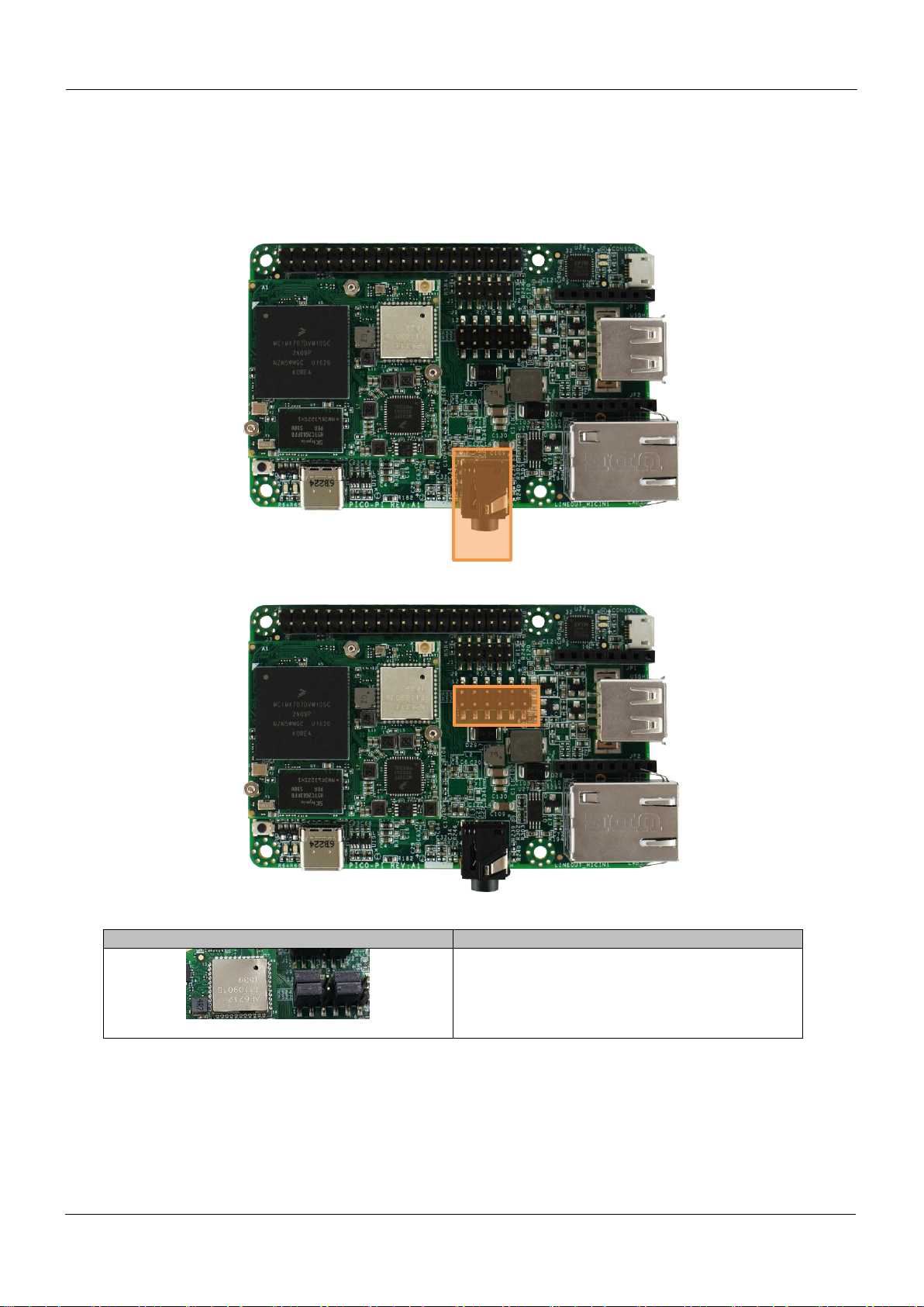
3.3. Gigabit Ethernet
The PICO-PI-IMX7 features a Gigabit Ethernet MAC compliant with the IEEE802.3-2002 standard.
Figure 13 - PICO-PI-IMX7 RJ-45 Network Connector Location
Page 14 of 38
Page 15
PICO-PI-IMX7 HARDWARE MANUAL – REV B1 – APR 5 2017
Detail
Description
Default Audio Selection is as below picture and
uses the primary I2S channel.
Please select the jumpers as the picture.
3.4. Audio Interface
The PICO-PI-IMX7 comes with an Audio jack which is compliant with the CTIA standard. A standard
mobile phone headset will work.
Figure 14 - PICO-PI-IMX7 Audio Jack Location
Figure 15 - PICO-PI-IMX7 Audio I2S Signal Location
Page 15 of 38
Page 16

PICO-PI-IMX7 HARDWARE MANUAL – REV B1 – APR 5 2017
3.5. Universal Serial Bus (USB) Host Interface
The PICO-PI-IMX7 features a standard USB 2.0 Host Connector.
Figure 16 - PICO-PI-IMX7 USB HOST Connector Location
3.6. Universal Serial Bus (USB) OTG Interface
The PICO-PI-IMX7 incorporates a single USB Host/OTG controller which also function as the system
power input.
The signals are routed to a USB Type-C connector.
Figure 17- PICO-PI-IMX7 USB OTG Type-C Connector Location
Page 16 of 38
Page 17

PICO-PI-IMX7 HARDWARE MANUAL – REV B1 – APR 5 2017
3.7. Debug Interface
The PICO-PI-IMX7 serial debug interface can be easily connected with a micro-USB cable.
The debug interface can be found on the PICO-PI-IMX7 at the following physical location and in
software can be accessed over UART5.
Figure 18 – PICO-PI-IMX7 Serial Debug Location
Page 17 of 38
Page 18

PICO-PI-IMX7 HARDWARE MANUAL – REV B1 – APR 5 2017
Boot from eMMC
Serial Boot Loader
3.8. Serial Boot or eMMC Boot Control Pins
The PICO-PI-IMX7 has a number of pins to override the default boot media (eMMC) and enter in
Serial Boot Loader mode.
Figure 19 - PICO-PI-IMX7 Boot Control Pins
Page 18 of 38
Page 19

PICO-PI-IMX7 HARDWARE MANUAL – REV B1 – APR 5 2017
PIN
Signal
V
I/O
Description
JP1_1
NC
Not Connected
JP1_2
RESET
3V3
I
Reset power signal
JP1_3
NC
Not Connected
JP1_4
ECSPI_SCLK
3V3
O
Serial Peripheral Interface clock signal
JP1_5
ECSPI_MISO
3V3
I
Serial Peripheral Interface master input slave
output signal
JP1_6
ECSPI_MOSI
3V3
O
Serial Peripheral Interface master output slave
input signal
JP1_7
3V3 Power
3V3
P
3V3 Power
JP1_8
GND
P Ground
PIN
Signal
V
I/O
Description
JP2_1
PWM7OUT
3V3
I/O
General Purpose Input Output with PWM control
JP2_2
GPIO
3V3
I/O
General Purpose Input Output
JP2_3
UART_RX
3V3
I
Universal Asynchronous Receive Transmit receive
data signal
JP2_4
UART_TXD
3V3
O
Universal Asynchronous Receive Transmit
transmit data signal
JP2_5
I2C_SCL
3V3
I/O
I2C bus clock line
JP2_6
I2C_SDA
3V3
I/O
I2C bus data line
JP2_7
5V Power
5V
P
5V Power
JP2_8
GND
P Ground
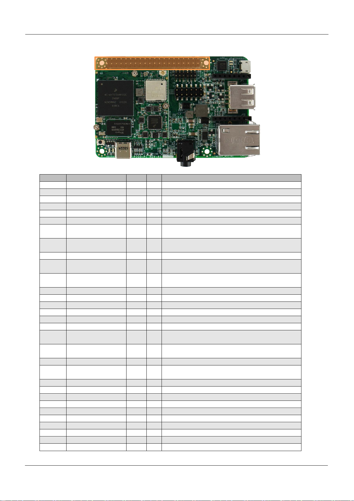
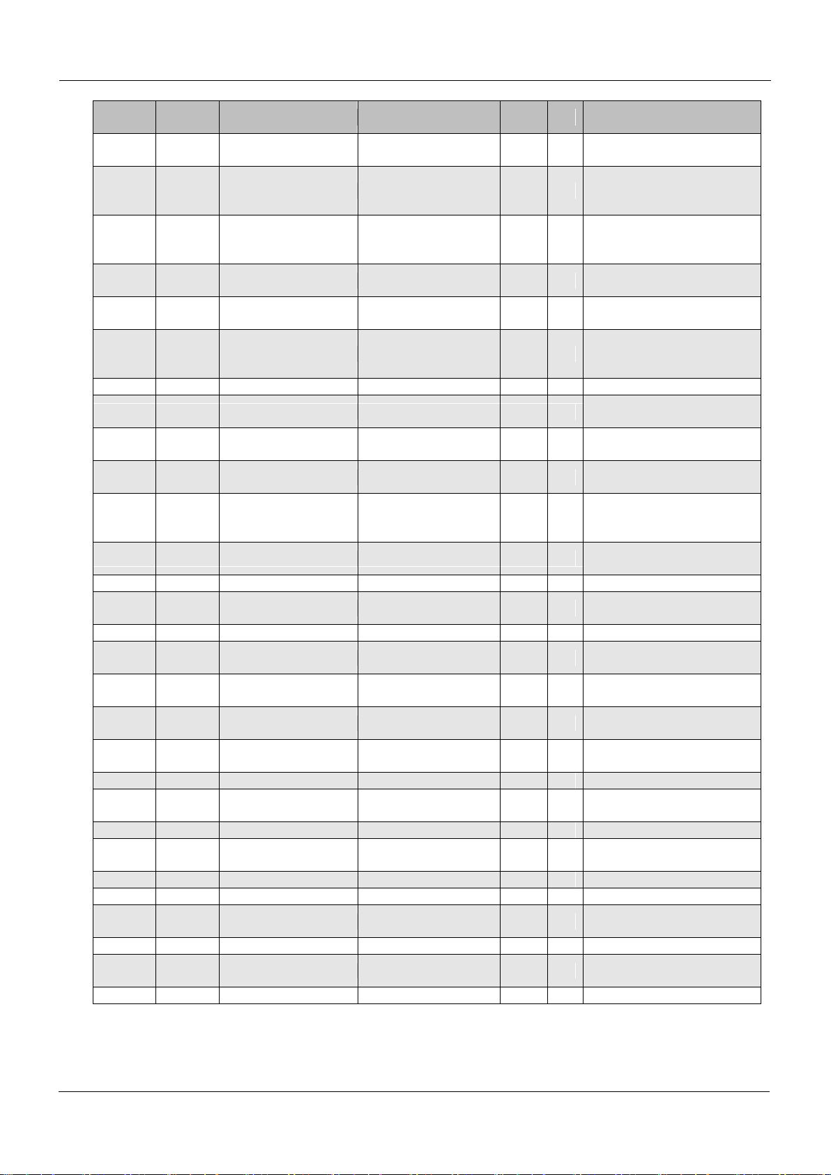
3.9. Expansion Header Pins
The PICO-PI-IMX7 has a number of expansion headers that can be used to connect sensors, motors,
and external devices.
Figure 20 - PICO-PI-IMX7 Mikrobus Header Location
Page 19 of 38
Page 20
PICO-PI-IMX7 HARDWARE MANUAL – REV B1 – APR 5 2017
PIN
Signal
V
I/O
Description
JP8_1
3V3 Power
3V3
P
3V3 Power
JP8_2
5V Power
5V
P
5V Power
JP8_3
I2C_SDA
3V3
I/O
I2C bus data line
JP8_4
5V Power
5V
P
5V Power
JP8_5
I2C_SCL
3V3
I/O
I2C bus clock line
JP8_6
GND
P Ground
JP8_7
UART_RTS
3V3
O
Universal Asynchronous Receive Transmit
request to send signal
JP8_8
UART_TXD
3V3
O
Universal Asynchronous Receive Transmit
transmit data signal
JP8_9
GND
P Ground
JP8_10
UART_RXD
3V3
I
Universal Asynchronous Receive Transmit receive
data signal
JP8_11
UART_CTS
3V3
O
Universal Asynchronous Receive Transmit clear to
send signal
JP8_12
PWM_OUT
3V3
I/O
General Purpose Input Output with PWM control
JP8_13
GPIO
3V3
I/O
General Purpose Input Output
JP8_14
GND
P Ground
JP8_15
NC
Not Connected
JP8_16
CAN_TX
3V3
I/O
CAN (controller Area Network) transmit signal
JP8_17
3V3 Power
3V3
P
3V3 Power
JP8_18
CAN_RX
3V3
I/O
CAN (controller Area
Network) receive signal
JP8_19
ECSPI_MOSI
3V3
O
Serial Peripheral Interface master output slave
input signal
JP8_20
GND
P Ground
JP8_21
ECSPI_MISO
3V3
I
Serial Peripheral Interface master input slave
output signal
JP8_22
NC
Not Connected
JP8_23
ECSPI_SCLK
3V3
O
Serial Peripheral Interface clock signal
JP8_24
NC
Not Connected
JP8_25
GND
P Ground
JP8_26
ECSPI_SS0
3V3
I/O
Serial Peripheral Interface Chip Select 1 signal
JP8_27
I2C_SDA
3V3
I/O
I2C bus data line
JP8_28
I2C_SCL
3V3
I/O
I2C bus clock line
JP8_29
GPIO
3V3
I/O
General Purpose Input Output
JP8_30
GND
P Ground
JP8_31
GPIO
3V3
I/O
General Purpose Input Output
Figure 21 - PICO-PI-IMX7 Expansion Header Location
Page 20 of 38
Page 21

PICO-PI-IMX7 HARDWARE MANUAL – REV B1 – APR 5 2017
JP8_32
GPIO
3V3
I/O
General Purpose Input Output
JP8_33
PWM_OUT
3V3
I/O
General Purpose Input Output with PWM control
JP8_34
GND
P Ground
JP8_35
GPIO
3V3
I/O
General Purpose Input Output
JP8_36
GPIO
3V3
I/O
General Purpose Input Output
JP8_37
GPIO
3V3
I/O
General Purpose Input Output
JP8_38
CAN_TX
3V3
I/O
CAN (controller Area Network) transmit signal
JP8_39
GND
P Ground
JP8_40
CAN_RX
3V3
I/O
CAN (controller Area Network) receive signal
Page 21 of 38
Page 22

PICO-PI-IMX7 HARDWARE MANUAL – REV B1 – APR 5 2017
Manufacturer
Partnumber
Description
TechNexion
TDP0500T800480PCAP
5 INCH 800 x 480 PCAP MULTI TOUCH LCD
PANEL INCLUDING TOUCH CABLE
TechNexion
TDP0700T800480PCAP
7 INCH 800 x 480 PCAP MULTI TOUCH LCD
PANEL INCLUDING TOUCH CABLE
5 INCH
7 INCH
1 – 8 : ON
2 – 7 : OFF
3 – 6 : ON
4 – 5 : OFF
1 – 8 : ON
2 – 7 : ON
3 – 6 : ON
4 – 5 : OFF
3.10. Display and Touch Connector
The PICO-PI-IMX7 features a Touch and RGB TTL Display interface that can be connected directly to
a multi-touch 24-bit LCD panel.
The following LCD displays have been tested:
Figure 22 - PICO-PI-IMX7 LCD Display FPC Connector Location
Page 22 of 38
Page 23

PICO-PI-IMX7 HARDWARE MANUAL – REV B1 – APR 5 2017
PIN
Signal
V
I/O
Description
LCD1_1
VLED+
21V7
LED Backlight Voltage
LCD1_2
VLED+
21V7
LED Backlight Voltage
LCD1_3
VLED-
GND
P
Ground
LCD1_4
VLED-
GND
P
Ground
LCD1_5
GND
P Ground
LCD1_6
VCOM
4V09
Common Voltage
LCD1_7
DVDD
3V3
Power for Digital Circuit
LCD1_8
MODE
3V3
DE/SYNC mode select
LCD1_9
LCDIF_ENABLE
3V3
O
LCD dot enable pin
signal
LCD1_10
LCDIF_VSYNC
3V3
O
LCD Vertical
Synchronization
LCD1_11
LCDIF_HSYNC
3V3
O
LCD Horizontal
Synchronization
LCD1_12
LCDIF_DATA7
3V3
O
LCD Pixel Data bit 7
LCD1_13
LCDIF_DATA6
3V3
O
LCD Pixel Data bit 6
LCD1_14
LCDIF_DATA5
3V3
O
LCD Pixel Data bit 5
LCD1_15
LCDIF_DATA4
3V3
O
LCD Pixel Data bit 4
LCD1_16
LCDIF_DATA3
3V3
O
LCD Pixel Data bit 3
LCD1_17
LCDIF_DATA2
3V3
O
LCD Pixel Data bit 2
LCD1_18
LCDIF_DATA1
3V3
O
LCD Pixel Data bit 1
LCD1_19
LCDIF_DATA0
3V3
O
LCD Pixel Data bit 0
LCD1_20
LCDIF_DATA15
3V3
O
LCD Pixel Data bit 15
LCD1_21
LCDIF_DATA14
3V3
O
LCD Pixel Data bit 14
LCD1_22
LCDIF_DATA13
3V3
O
LCD Pixel Data bit 13
LCD1_23
LCDIF_DATA12
3V3
O
LCD Pixel Data bit 12
LCD1_24
LCDIF_DATA11
3V3
O
LCD Pixel Data bit 11
LCD1_25
LCDIF_DATA10
3V3
O
LCD Pixel Data bit 10
LCD1_26
LCDIF_DATA9
3V3
O
LCD Pixel Data bit 9
LCD1_27
LCDIF_DATA8
3V3
O
LCD Pixel Data bit 8
LCD1_28
LCDIF_DATA23
3V3
O
LCD Pixel Data bit 23
LCD1_29
LCDIF_DATA22
3V3
O
LCD Pixel Data bit 22
LCD1_30
LCDIF_DATA21
3V3
O
LCD Pixel Data bit 21
LCD1_31
LCDIF_DATA20
3V3
O
LCD Pixel Data bit 20
LCD1_32
LCDIF_DATA19
3V3
O
LCD Pixel Data bit 19
LCD1_33
LCDIF_DATA18
3V3
O
LCD Pixel Data bit 18
LCD1_34
LCDIF_DATA17
3V3
O
LCD Pixel Data bit 17
LCD1_35
LCDIF_DATA16
3V3
O
LCD Pixel Data bit 16
LCD1_36
GND
P Ground
LCD1_37
LCDIF_CLK
3V3
O
LCD Pixel Clock
LCD1_38
GND
P Ground
LCD1_39
L/R
3V3
I
Left / Right Selection
LCD1_40
U/D
3V3
I
Up / Down Selection
LCD1_41
VGH
16V0
P
Gate ON Voltage
LCD1_42
VGL
-6V0
P
Gate OFF Voltage
LCD1_43
AVDD
10V4
P
Power for Analog Circuit
LCD1_44
RESET
3V3
I
Reset power signal
LCD1_45
NC
Not Connected
LCD1_46
VCOM
3V3
I
Common voltage
LCD1_47
DITHB
3V3
I
Dithering function
LCD1_48
GND
P Ground
LCD1_49
NC
Not Connected
LCD1_50
NC
Not Connected
Page 23 of 38
Page 24

PICO-PI-IMX7 HARDWARE MANUAL – REV B1 – APR 5 2017
PIN
Signal
V
I/O
Description
TOUCH_1
I2C1_SDA
3V3
I/O
I2C bus data line
TOUCH_2
I2C1_SCL
3V3
I/O
I2C bus clock line
TOUCH_3
3V3 Power
3V3
P
3V3 Power
TOUCH_4
GPIO4_IO29
3V3
I/O
General Purpose Input
Output
TOUCH_5
GPIO4_IO24
3V3
I/O
General Purpose Input
Output
TOUCH_6
GND
P Ground
Figure 23 - PICO-PI-IMX7 Touch Panel Connector Location
Page 24 of 38
Page 25

PICO-PI-IMX7 HARDWARE MANUAL – REV B1 – APR 5 2017
Manufacturer
Partnumber
Description
TechNexion
CAM-OV5645
5MP OMNIVISION CAMERA MODULE WITH
20CM FPC CABLE
3.11. MIPI Connector
The PICO-PI-IMX7 features a MIPI CSI and MIPI DSI connector to connect to MIPI devices.
The following Camera modules have been tested:
Figure 24 - PICO-PI-IMX7 Touch Panel Connector Location
Page 25 of 38
Page 26

PICO-PI-IMX7 HARDWARE MANUAL – REV B1 – APR 5 2017
PIN
Signal
V
I/O
Description
CAM_1
CSI_CLK0P
CMOS
2.5V
I
MIPI Camera Serial Interface clock pair positive
signal
CAM_2
CSI_CLK0M
CMOS
2.5V
I
MIPI Camera Serial Interface clock pair negative
signal
CAM_3
GND
GND
P
Ground
CAM_4
CSI_D0P
CMOS
2.5V
I
MIPI Camera Serial Interface data pair 0 positive
signal
CAM_5
CSI_D0M
CMOS
2.5V
I
MIPI Camera Serial Interface data pair 0
negative signal
CAM_6
GND
GND
P
Ground
CAM_7
CSI_D1P
CMOS
2.5V
I
MIPI Camera Serial Interface data pair 1 positive
signal
CAM_8
CSI_D1M
CMOS
2.5V
I
MIPI Camera Serial Interface data pair 1
negative signal
CAM_9
GND
GND
P
Ground
CAM_10
CSI_D2P
CMOS
2.5V
I
MIPI Camera Serial Interface data pair 2 positive
signal
CAM_11
CSI_D2M
CMOS
2.5V
I
MIPI Camera Serial Interface data pair 2
negative signal
CAM_12
GND
GND
P
Ground
CAM_13
CSI_D3P
CMOS
2.5V
I
MIPI Camera Serial Interface data pair 3 positive
signal
CAM_14
CSI_D3M
CMOS
2.5V
I
MIPI Camera Serial Interface data pair 3
negative signal
CAM_15
GND
GND
P
Ground
CAM_16
DSI_D1P
O
MIPI Display Serial Interface data pair 1 positive
signal
CAM_17
DSI_D1M
O
MIPI Camera Serial Interface data pair 1
negative signal
CAM_18
GND
GND
P
Ground
CAM_19
DSI_D0P
CMOS
2.5V
O
MIPI Display Serial Interface data pair 0 positive
signal
CAM_20
DSI_D0M
CMOS
2.5V
O
MIPI Camera Serial Interface data pair 0
negative signal
CAM_21
GND
GND
P
Ground
CAM_22
DSI_CLK0P
CMOS
2.5V
O
MIPI Display Serial Interface clock pair positive
signal
CAM_23
DSI_CLK0M
CMOS
2.5V
O
MIPI Camera Serial Interface clock pair negative
signal
CAM_24
GND
GND
P
Ground
CAM_25
I2C_SCL
CMOS
3.3V
I/O
I2C bus clock line
CAM_26
I2C_SDA
CMOS
3.3V
I/O
I2C bus data line
CAM_27
3.3V
P
Power Supply 3.3VDC
CAM_28
3.3V
P
Power Supply 3.3VDC
CAM_29
GPIO
CMOS
3.3V
I/O
General Purpose Input Output
CAM_30
GPIO
CMOS
3.3V
I/O
General Purpose Input Output
CAM_31
GPIO
CMOS
3.3V
I/O
General Purpose Input Output
CAM_32
VCC
5V P Power Supply 5VDC ± 5%
CAM_33
VCC
5V P Power Supply 5VDC ± 5%
Page 26 of 38
Page 27

PICO-PI-IMX7 HARDWARE MANUAL – REV B1 – APR 5 2017
PIN
CPU
BALL
CPU PAD NAME
Signal
V
I/O
Description
E1_1
GND
P Ground
E1_2
VSYS
P
System input power (4.0
to 5.25V)
E1_3
B7
USB_OTG1_ID
USB_OTG1_ID
3V3
I
USB OTG ID Pin
E1_4
VSYS
P
System input power (4.0
to 5.25V)
E1_5
GND
P Ground
E1_6
VSYS
P
System input power (4.0
to 5.25V)
E1_7
N5
CLK_32K_OUT
CLK_32K_OUT
3V3
E1_8
3V3 P
System 3.3V Output
E1_9
GND
P Ground
E1_10
3V3 P
System 3.3V Output
E1_11
GND
P Ground
E1_12
1V8 P
System 1.8V Output
(same as E1 connector
I/O voltage levels)
E1_13
GND
P Ground
E1_14
VSYS
P
System input power (4.0
to 5.25V)
E1_15
GND
P Ground
E1_16
B8
USB_OTG1_DP
USB_OTG1_DP
3V3
I/O
Universal Serial Bus
differential pair positive
signal
E1
X1
X2
4. PICO Compute Module Pin Assignment
The PICO-IMX7 has three 70-pin Hirose board to board connectors.
Page 27 of 38
Page 28
PICO-PI-IMX7 HARDWARE MANUAL – REV B1 – APR 5 2017
PIN
CPU
BALL
CPU PAD NAME
Signal
V
I/O
Description
E1_17
AC8
ONOFF
ONOFF
3V3
I
Power ON button input
signal
E1_18
A8
USB_OTG1_DN
USB_OTG1_DN
3V3
I/O
Universal Serial Bus
differential pair negative
signal
E1_19
M1
UART3_RXD
USB_OTG1_OC
1V8
I
Over current detect input
pin to monitor USB power
over current
E1_20
C8
USB_OTG1_VBUS
USB_OTG1_VBUS
5V
I/O
Universal Serial Bus
power
E1_21
M2
UART3_TXD
USB_OTG1_PWR
1V8
O
Universal Serial Bus
power enable
E1_22
L1
I2C4_SCL
UART5_RXD
1V8
I
Universal Asynchronous
Receive Transmit receive
data signal
E1_23
VCC_RTC
3V3
P
RTC Power
E1_24
P20
EPDC1_DATA00
GPIO2_IO00
1V8
I/O
General Purpose Input
Output
E1_25
M21
EPDC_D06
GPIO2_IO06
1V8
I/O
General Purpose Input
Output
E1_26
P21
EPDC1_D01
GPIO2_IO01
1V8
I/O
General Purpose Input
Output
E1_27
L2
I2C4_SDA
UART5_TXD
1V8
O
Universal Asynchronous
Receive Transmit transmit
data signal
E1_28
N20
EPDC1_D02
GPIO2_IO02
1V8
I/O
General Purpose Input
Output
E1_29
NC
Not Connected
E1_30
N21
EPDC1_D03
GPIO2_IO03
1V8
I/O
General Purpose Input
Output
E1_31
NC
Not Connected
E1_32
N22
EPDC1_D04
GPIO2_IO04
1V8
I/O
General Purpose Input
Output
E1_33
R1
GPIO1_IO08
PWM1_OUT
1V8
O
General Purpose Input
Output with PWM control
E1_34
M20
EPDC1_D05
GPIO2_IO05
1V8
I/O
General Purpose Input
Output
E1_35
R2
GPIO1_IO09
PWM2_OUT
1V8
O
General Purpose Input
Output with PWM control
E1_36
PMIC
RESET
RESET
1V8
I
Reset power signal
E1_37
R5
GPIO1_IO10
PWM3_OUT
1V8
O
General Purpose Input
Output with PWM control
E1_38
NC
Not Connected
E1_39
T1
GPIO1_IO11
PWM4_OUT
1V8
O
General Purpose Input
Output with PWM control
E1_40
NC
Not Connected
E1_41
L3
UART1_RXD
I2C1_SCL
1V8
I/O
I2C bus clock line
E1_42
L22
EPDC1_D12
GPIO2_IO12
1V8
I/O
General Purpose Input
Output
E1_43
L4
UART1_TXD
I2C1_SDA
1V8
I/O
I2C bus data line
E1_44
L21
EPDC1_D13
GPIO2_IO13
1V8
I/O
General Purpose Input
Output
E1_45
L5
UART2_RXD
I2C2_SCL
1V8
I/O
I2C bus clock line
Page 28 of 38
Page 29

PICO-PI-IMX7 HARDWARE MANUAL – REV B1 – APR 5 2017
PIN
CPU
BALL
CPU PAD NAME
Signal
V
I/O
Description
E1_46
L25
EPDC1_DATA09
UART6_TX_DATA
1V8
O
Universal Asynchronous
Receive Transmit transmit
data signal
E1_47
L6
UART2_TXD
I2C2_SDA
1V8
I/O
I2C bus data line
E1_48
M22
EPDC1_D07
GPIO2_IO07
1V8
I/O
General Purpose Input
Output
E1_49
NC
Not Connected
E1_50
D16
ENET1_TX_CLK
SAI1_RX_DATA
1V8
I
Integrated Interchip
Sound (I2S) channel
receive data line
E1_51
M6
UART3_CTS
ECSPI1_SS0
1V8
O
Serial Peripheral Interface
Chip Select Signal
E1_52
D15
ENET1_RX_CLK
SAI1_TX_BCLK
1V8
O
Integrated Interchip
Sound (I2S) channel word
clock signal
E1_53
K3
I2C2_SDA
ECSPI3_SS0
1V8
O
Serial Peripheral Interface
Chip Select signal
E1_54
E19
ENET1_CRS
SAI1_TX_SYNC
1V8
I/O
Integrated Interchip
Sound (I2S) channel
frame synchronization
signal
E1_55
K2
I2C2_SCL
ECSPI3_SCLK
1V8
I/O
Serial Peripheral Interface
clock signal
E1_56
D19
ENET1_COL
SAI1_TX_DATA
1V8
O
Integrated Interchip
Sound (I2S) channel
transmit data line
E1_57
K1
I2C1_SDA
ECSPI3_MOSI
1V8
I/O
Serial Peripheral Interface
master output slave input
signal
E1_58
B5
SD1_CLK
SD1_CLK
1V8
I/O
MMC/SDIO Clock
E1_59
J2
I2C1_SCL
ECSPI3_MISO
1V8
I/O
Serial Peripheral Interface
master input slave output
signal
E1_60
C6
SD1_CD_B
SD1_CD_B
1V8
I
SD Card detect input
(Active low)
E1_61
M23
EPDC1_DATA08
UART6_RX_DATA
1V8
I
Universal Asynchronous
Receive Transmit receive
data signal
E1_62
C5
SD1_CMD
SD1_CMD
1V8
I/O
MMC/SDIO Command
E1_63
L24
EPDC1_DATA10
UART6_RTS_B
1V8
I
Universal Asynchronous
Receive Transmit request
to send signal
E1_64
A4
SD1_DATA2
SD1_DATA2
1V8
I/O
MMC/SDIO Data bit 2
E1_65
L23
EPDC1_DATA11
UART6_CTS_B
1V8
O
Universal Asynchronous
Receive Transmit clear to
send signal
E1_66
A5
SD1_DATA0
SD1_DATA0
1V8
I/O
MMC/SDIO Data bit 0
E1_67
NC
Not Connected
E1_68
D5
SD1_DATA3
SD1_DATA3
1V8
I/O
MMC/SDIO Data bit 3
E1_69
NC
Not Connected
E1_70
D6
SD1_DATA1
SD1_DATA1
1V8
I/O
MMC/SDIO Data bit 1
Page 29 of 38
Page 30

PICO-PI-IMX7 HARDWARE MANUAL – REV B1 – APR 5 2017
PIN
CPU
BALL
CPU PAD NAME
Signal
V
I/O
Description
X1_1
GND
P Ground
X1_2
GND
P Ground
X1_3
NC
Not Connected
X1_4
NC
Not Connected
X1_5
NC
Not Connected
X1_6
NC
Not Connected
X1_7
GND
P Ground
X1_8
G23
LCD1_DATA23
LCD_DATA23
3V3
O
LCD Pixel Data bit 23
X1_9
NC
Not Connected
X1_10
D25
LCD1_DATA22
LCD_DATA22
3V3
O
LCD Pixel Data bit 22
X1_11
NC
Not Connected
X1_12
E24
LCD1_DATA21
LCD_DATA21
3V3
O
LCD Pixel Data bit 21
X1_13
GND
P Ground
X1_14
C25
LCD1_DATA20
LCD_DATA20
3V3
O
LCD Pixel Data bit 20
X1_15
NC
Not Connected
X1_16
D24
LCD1_DATA19
LCD_DATA19
3V3
O
LCD Pixel Data bit 19
X1_17
NC
Not Connected
X1_18
E23
LCD1_DATA18
LCD_DATA18
3V3
O
LCD Pixel Data bit 18
X1_19
GND
P Ground
X1_20
G21
LCD1_DATA17
LCD_DATA17
3V3
O
LCD Pixel Data bit 17
X1_21
NC
Not Connected
X1_22
B25
LCD1_DATA16
LCD_DATA16
3V3
O
LCD Pixel Data bit 16
X1_23
NC
Not Connected
X1_24
C24
LCD1_DATA15
LCD_DATA15
3V3
O
LCD Pixel Data bit 15
X1_25
GND
P Ground
X1_26
D23
LCD1_DATA14
LCD_DATA14
3V3
O
LCD Pixel Data bit 14
X1_27
NC
Not Connected
X1_28
E22
LCD1_DATA13
LCD_DATA13
3V3
O
LCD Pixel Data bit 13
X1_29
NC
Not Connected
X1_30
F21
LCD1_DATA12
LCD_DATA12
3V3
O
LCD Pixel Data bit 12
X1_31
GND
P Ground
X1_32
G20
LCD1_DATA11
LCD_DATA11
3V3
O
LCD Pixel Data bit 11
X1_33
C3
SD2_WP
ENET1_MDC
3V3
Management data
clock reference
X1_34
B24
LCD1_DATA10
LCD_DATA10
3V3
O
LCD Pixel Data bit 10
X1_35
D3
SD2_CD_B
ENET1_MDIO
3V3
Management data
X1_36
C23
LCD1_DATA09
LCD_DATA09
3V3
O
LCD Pixel Data bit 9
X1_37
G1
SD3_RESET_B
GPIO6_IO11
3V3
Ethernet reset
X1_38
E21
LCD1_DATA08
LCD_DATA08
3V3
O
LCD Pixel Data bit 8
X1_39
J1
SD3_STROBE
GPIO6_IO10
3V3
Ethernet interrupt
output
X1_40
F20
LCD1_DATA07
LCD_DATA07
3V3
O
LCD Pixel Data bit 7
X1_41
N2
GPIO1_IO01
CCM_ENET_REF_CLK3
3V3
Synchronous Ethernet
recovered clock
X1_42
A24
LCD1_DATA06
LCD_DATA06
3V3
O
LCD Pixel Data bit 6
X1_43
E16
ENET1_TX_CTL
RGMII1_TX_CTL
1V8
O
RGMII transmit enable
X1_44
B23
LCD1_DATA05
LCD_DATA05
3V3
O
LCD Pixel Data bit 5
X1_45
E15
ENET1_RX_CTL
RGMII1_RX_CTL
1V8
I
RGMII receive data
valid
X1_46
C22
LCD1_DATA04
LCD_DATA04
3V3
O
LCD Pixel Data bit 4
Page 30 of 38
Page 31

PICO-PI-IMX7 HARDWARE MANUAL – REV B1 – APR 5 2017
PIN
CPU
BALL
CPU PAD NAME
Signal
V
I/O
Description
X1_47
GND
P Ground
X1_48
A23
LCD1_DATA03
LCD_DATA03
3V3
O
LCD Pixel Data bit 3
X1_49
F16
ENET1_TXC
RGMII1_TXC
1V8
O
RGMII transmit clock
X1_50
B22
LCD1_DATA02
LCD_DATA02
3V3
O
LCD Pixel Data bit 2
X1_51
F17
ENET1_TDATA0
RGMII1_TD0
1V8
O
RGMII transmit data 0
X1_52
A22
LCD1_DATA01
LCD_DATA01
3V3
O
LCD Pixel Data bit 1
X1_53
E17
ENET1_TDATA1
RGMII1_TD1
1V8
O
RGMII transmit data 1
X1_54
D21
LCD1_DATA00
LCD_DATA00
3V3
O
LCD Pixel Data bit 0
X1_55
E18
ENET1_TDATA2
RGMII1_TD2
1V8
O
RGMII transmit data 2
X1_56
C21
LCD1_RESET
LCD_RS
3V3
O
LCD backlight
enable/disable
X1_57
D18
ENET1_TDATA3
RGMII1_TD3
1V8
O
RGMII transmit data 3
X1_58
E25
LCD1_HSYNC
LCD_HSYNC
3V3
O
LCD Horizontal
Synchronization
X1_59
GND
P Ground
X1_60
F25
LCD1_ENABLE
LCD_ENABLE
3V3
O
LCD dot enable pin
signal
X1_61
F15
ENET1_RXC
RGMII1_RXC
1V8
I
RGMII receive clock
X1_62
F24
LCD1_VSYNC
LCD_VSYNC
3V3
O
LCD Vertical
Synchronization
X1_63
E14
ENET1_RDATA0
RGMII1_RD0
1V8
I
RGMII transmit data 0
X1_64
E20
LCD1_CLK
LCD_CLK
3V3
O
LCD Pixel Clock
X1_65
F14
ENET1_RDATA1
RGMII1_RD1
1V8
I
RGMII receive data 1
X1_66
T1
GPIO1_IO11
PWM4_OUT
3V3
O
LCD Backlight brightness
Control
X1_67
D13
ENET1_RDATA2
RGMII1_RD2
1V8
I
RGMII receive data 2
X1_68
P2
GPIO1_IO06
GPIO1_IO06
3V3
O
LCD Voltage On
X1_69
E13
ENET1_RDATA3
RGMII1_RD3
1V8
I
RGMII receive data 3
X1_70
GND
P Ground
Page 31 of 38
Page 32

PICO-PI-IMX7 HARDWARE MANUAL – REV B1 – APR 5 2017
PIN
CPU
BALL
CPU PAD NAME
Signal
V
I/O
Description
X2_1
GND
P Ground
X2_2
GND
P Ground
X2_3
G20
BT_CFG11
BT_CFG11
1V8
I
Boot Select pin
X2_4
NC
Not Connected
X2_5
C22
BT_CFG4
BT_CFG4
1V8
I
Boot Select pin
X2_6
NC
Not Connected
X2_7
F21
BT_CFG12
BT_CFG12
1V8
I
Boot Select pin
X2_8
GND
P Ground
X2_9
E22
BT_CFG13
BT_CFG13
1V8
I
Boot Select pin
X2_10
NC
Not Connected
X2_11
GND
P Ground
X2_12
NC
Not Connected
X2_13
C12
SAI1_RXFS
I2C4_SCL
3V3
I/O
I2C bus clock line
X2_14
GND
P Ground
X2_15
D12
SAI1_RXC
I2C4_SDA
3V3
I/O
I2C bus data line
X2_16
NC
Not Connected
X2_17
GND
P Ground
X2_18
NC
Not Connected
X2_19
C11
SAI1_TXC
FLEXCAN1_TX
3V3
O
CAN (controller Area
Network) transmit signal
X2_20
GND
P Ground
X2_21
E12
SAI1_RXD
FLEXCAN1_RX
3V3
I
CAN (controller Area
Network) receive signal
X2_22
NC
Not Connected
X2_23
GND
P Ground
X2_24
NC
Not Connected
X2_25
E11
SAI1_TXD
FLEXCAN2_TX
3V3
O
CAN (controller Area
Network) transmit signal
X2_26
GND
P Ground
X2_27
D11
SAI1_TXFS
FLEXCAN2_RX
3V3
I
CAN (controller Area
Network) receive signal
X2_28
NC
Not Connected
X2_29
GND
P Ground
X2_30
NC
Not Connected
X2_31
A15
MIPI_CSI_CLK_N
2V5
I
MIPI Camera Serial
Interface clock pair
negative signal
X2_32
GND
P Ground
X2_33
B15
MIPI_CSI_CLK_P
2V5
I
MIPI Camera Serial
Interface clock pair
positive signal
X2_34
NC
Not Connected
X2_35
A16
MIPI_CSI_D0_N
2V5
I
MIPI Camera Serial
Interface data pair 0
negative signal
X2_36
NC
Not Connected
X2_37
B16
MIPI_CSI_D0_P
2V5
I
MIPI Camera Serial
Interface data pair 0
positive signal
X2_38
GND
P Ground
X2_39
B14
MIPI_CSI_D1_P
2V5
I
MIPI Camera Serial
Interface data pair 1
positive signal
X2_40
NC
Not Connected
Page 32 of 38
Page 33

PICO-PI-IMX7 HARDWARE MANUAL – REV B1 – APR 5 2017
PIN
CPU
BALL
CPU PAD NAME
Signal
V
I/O
Description
X2_41
A14
MIPI_CSI_D1_N
2V5
I
MIPI Camera Serial
Interface data pair 1
negative signal
X2_42
NC
Not Connected
X2_43
NC
Not Connected
X2_44
GND
P Ground
X2_45
NC
Not Connected
X2_46
A10
USB_OTG2_DN
3V3
I/O
Universal Serial Bus
differential pair negative
signal
X2_47
NC
Not Connected
X2_48
B10
USB_OTG2_DP
3V3
I/O
Universal Serial Bus
differential pair positive
signal
X2_49
NC
Not Connected
X2_50
C10
USB_OTG2_VBUS
5V
I/O
Universal Serial Bus
power
X2_51
GND
P Ground
X2_52
M5
UART3_RTS
USB_OTG2_OC
3V3
I
Active low input, to inform
USB overcurrent condition
(low = overcurrent
detected)
X2_53
B20
MIPI_DSI_D0_P
2V5
O
MIPI Display Serial
Interface data pair 0
positive signal
X2_54
GND
P Ground
X2_55
A20
MIPI_DSI_D0_N
2V5
O
MIPI Display Serial
Interface data pair 0
negative signal
X2_56
AB10
PCIE_REFCLKOUT_P
2V5
O
PCI Express clock
differential pair positive
signal
X2_57
B18
MIPI_DSI_D1_P
2V5
O
MIPI Display Serial
Interface data pair 1
positive signal
X2_58
AC10
PCIE_REFCLKOUT_N
2V5
O
PCI Express clock
differential pair negative
signal
X2_59
A18
MIPI_DSI_D1_N
2V5
O
MIPI Display Serial
Interface data pair 1
negative signal
X2_60
GND
P Ground
X2_61
A19
MIPI_DSI_CLK_N
2V5
O
MIPI Display Serial
Interface clock pair
negative signal
X2_62
AB11
PCIE_TX_P
2V5
O
PCI Express Transmit
output differential pair
positive signal
X2_63
B19
MIPI_DSI_CLK_P
2V5
O
MIPI Display Serial
Interface clock pair
positive signal
X2_64
AC11
PCIE_TX_N
2V5
O
PCI Express Transmit
output differential pair
negative signal
X2_65
P1
GPIO1_IO05
GPIO1_IO05
3V3
I/O
General Purpose Input
Output
Page 33 of 38
Page 34

PICO-PI-IMX7 HARDWARE MANUAL – REV B1 – APR 5 2017
PIN
CPU
BALL
CPU PAD NAME
Signal
V
I/O
Description
X2_66
GND
P Ground
X2_67
N6
GPIO1_IO04
GPIO1_IO04
3V3
I/O
General Purpose Input
Output
X2_68
AD11
PCIE_RX_P
2V5
I
PCI Express Receive
input differential pair
positive signal
X2_69
N3
GPIO1_IO02
GPIO1_IO02
3V3
I/O
General Purpose Input
Output
X2_70
AE11
PCIE_RX_N
2V5
I
PCI Express Receive
input differential pair
negative signal
Page 34 of 38
Page 35

PICO-PI-IMX7 HARDWARE MANUAL – REV B1 – APR 5 2017
5. Disclaimer and Important Notice
Wandboard.org reserve the right to make corrections, modifications, enhancements, improvements,
and other changes to its products and services at any time and to discontinue any product or service
without notice. Customers should obtain the latest relevant information before placing orders and
should verify that such information is current and complete. All products are sold subject to
Wandboard.org terms and conditions of sale supplied at the time of order acknowledgment.
Wandboard.org warrants performance of its hardware products to the specifications applicable at the
time of sale in accordance with Wandboard.org standard warranty. Testing and other quality control
techniques are used to the extent Wandboard.org deems necessary to support this warranty. Except
where mandated by government requirements, testing of all parameters of each product is not
necessarily performed.
Wandboard.org assumes no liability for applications assistance or customer product design.
Customers are responsible for their products and applications using Wandboard.org components. To
minimize the risks associated with customer products and applications, customers should provide
adequate design and operating safeguards.
Wandboard.org does not warrant or represent that any license, either express or implied, is granted
under any Wandboard.org patent right, copyright, mask work right, or other Wandboard.org
intellectual property right relating to any combination, machine, or process in which Wandboard.org
products or services are used. Information published by Wandboard.org regarding third-party products
or services does not constitute a license from Wandboard.org to use such products or services or a
warranty or endorsement thereof. Use of such information may require a license from a third party
under the patents or other intellectual property of the third party, or a license from Wandboard.org
under the patents or other intellectual property of Wandboard.org.
Wandboard.org products are not authorized for use in safety-critical applications (such as life support)
where a failure of the Wandboard.org product would reasonably be expected to cause severe
personal injury or death, unless officers of the parties have executed an agreement specifically
governing such use. Buyers represent that they have all necessary expertise in the safety and
regulatory ramifications of their applications, and acknowledge and agree that they are solely
responsible for all legal, regulatory and safety-related requirements concerning their products and any
use of Wandboard.org products in such safety-critical applications, notwithstanding any applicationsrelated information or support that may be provided by Wandboard.org. Further, Buyers must fully
indemnify Wandboard.org and its representatives against any damages arising out of the use of
Wandboard.org products in such safety-critical applications.
Wandboard.org products are neither designed nor intended for use in military/aerospace applications
or environments unless the Wandboard.org products are specifically designated by Wandboard.org
as military grade or "enhanced plastic." Only products designated by Wandboard.org as military-grade
meet military specifications. Buyers acknowledge and agree that any such use of Wandboard.org
products which Wandboard.org has not designated as military-grade is solely at the Buyer's risk, and
that they are solely responsible for compliance with all legal and regulatory requirements in
connection with such use.
Wandboard.org products are neither designed nor intended for use in automotive applications or
environments unless the specific Wandboard.org products are designated by Wandboard.org as
compliant with ISO/TS 16949 requirements. Buyers acknowledge and agree that, if they use any nondesignated products in automotive applications, Wandboard.org will not be responsible for any failure
to meet such requirements.
Page 35 of 38
Page 36

PICO-PI-IMX7 HARDWARE MANUAL – REV B1 – APR 5 2017
6. Schematics
WANDBOARD DESIGN AND DISCLAIMER
These design materials referred to in this document are *NOT SUPPORTED* and DO NOT constitute
a reference design. "Community" support is available via resources at Wandboard.org forums.
THERE IS NO WARRANTY FOR THE DESIGN MATERIALS, TO THE EXTENT PERMITTED BY
APPLICABLE LAW. EXCEPT WHEN OTHERWISE STATED IN WRITING THE COPYRIGHT
HOLDERS AND/OR OTHER PARTIES PROVIDE THE DESIGN MATERIALS "AS IS" WITHOUT
WARRANTY OF ANY KIND, EITHER EXPRESSED OR IMPLIED, INCLUDING, BUT NOT LIMITED
TO, THE IMPLIED WARRANTIES OF MERCHANTABILITY AND FITNESS FOR A PARTICULAR
PURPOSE.THE ENTIRE RISK AS TO THE QUALITY AND PERFORMANCEOF THE DESIGN
MATERIALS IS WITH YOU. SHOULD THE DESIGN MATERIALS PROVE DEFECTIVE, YOU
ASSUME THE COST OF ALL NECESSARY SERVICING, REPAIR OR CORRECTION.
This board was designed as an evaluation and development tool. It was not designed with any other
application in mind. As such, these design materials may or may not be suitable for any other
purposes. If used, the design material becomes your responsibility as to whether or not it meets your
specific needs or your specific applications and may require changes to meet your requirements.
On the following pages, you will find the schematics of the PICO-IMX7 Compute Module and the
PICO-PI Carrier Baseboard.
Components marked with -x are not populated.
Page 36 of 38
Page 37

PICO-PI-IMX7 HARDWARE MANUAL – REV B1 – APR 5 2017
15.19
This device complies with Part 15 of the FCC Rules. Operation is subject to the following two
conditions: (1) this
device may not cause harmful interference, and (2) this device must accept any interference received,
including interference that may cause undesired operation.
15.105
This equipment has been tested and found to comply with the limits for a Class B digital device,
pursuant to part 15 of the FCC Rules. These limits are designed to provide reasonable protection
against harmful interference in a residential installation. This equipment generates, uses and can
radiate radio frequency energy and, if not installed and used in accordance with the instructions, may
cause harmful interference to radio communications. However, there is no guarantee that interference
will not occur in a particular installation. If this equipment does cause harmful interference to radio or
television reception, which can be determined by turning the equipment off and on, the user is
encouraged to try to correct the interference by one or more of the following measures:
—Reorient or relocate the receiving antenna.
—Increase the separation between the equipment and receiver.
—Connect the equipment into an outlet on a circuit different from that to which the receiver is
connected.
—Consult the dealer or an experienced radio/TV technician for help.
15.21
Any changes or modifications not expressly approved by the party responsible for compliance
could void the authority to operate
equipment.
This device and its antenna must not be co-located or operating in conjunction with any other
antenna or transmitter.
End-users and installers must be provided with antenna installation instructions and
transmitter operating conditions for satisfying RF
exposure compliance.
For product available in the USA/Canada market, only channel 1~11 can be operated.
Selection of other channels is not possible
FCC RF Radiation Exposure Statement:
Mobile Device
This equipment complies with FCC radiation exposure limits set forth for an uncontrolled
environment. This equipment should be installed and operated with minimum distance 20cm between
the radiator & your body.
Module
This module is intended for OEM integrator. The OEM integrator is still responsible for the FCC
compliance requirement of the end product, which integrates this module. 20cm minimum distance
has to be able to be maintained between the antenna and the users for the host this module is
integrated into. Under such configuration, the FCC radiation exposure limits set forth for an
population/uncontrolled environment can be satisfied.
Any changes or modifications not expressly approved by the manufacturer could void the user's
authority to operate this equipment.
USERS MANUAL OF THE END PRODUCT:
In the users manual of the end product, the end user has to be informed to keep at least 20cm
separation with the antenna while this end product is installed and operated. The end user has to be
informed that the FCC radio-frequency exposure guidelines for an uncontrolled environment can be
satisfied. The end user has to also be informed that any changes or modifications not expressly
approved by the manufacturer could void the user's authority to operate this equipment.
If the size of the end product is smaller than 8x10cm, then additional FCC part 15.19 statement is
required to be available in the users manual: This device complies with Part 15 of FCC rules.
Operation is subject to the following two conditions: (1) this device may not cause harmful interference
Page 37 of 38
Page 38

PICO-PI-IMX7 HARDWARE MANUAL – REV B1 – APR 5 2017
and (2) this device must accept any interference received, including interference that may cause
undesired operation.
LABEL OF THE END PRODUCT:
The final end product must be labeled in a visible area with the following " Contains TX FCC ID:
2AKZA-PICOIMX7. If the size of the end product is larger than 8x10cm, then the following FCC part
15.19 statement has to also be available on the label: This device complies with Part 15 of FCC rules.
Operation is subject to the following two conditions: (1) this device may not cause harmful interference
and (2) this device must accept any interference received, including interference that may cause
undesired operation.
Page 38 of 38
 Loading...