

Page 1
PICO-PI-IMX6UL
NXP i.MX6Ultralite
February 24, 2017
Page 2

PICO-PI-IMX6UL HARDWARE MANUAL – VER 1.00 – FEB 24 2017
Page 2 of 44
TABLE OF CONTENTS
1. PICO-PI-IMX6UL Product Overview ................................................................................................... 3
1.1. PICO-IMX6 System -on-Module Overview ................................................................................... 4
1.2. PICO-PI-IMX6UL Carrier Baseboard Overview ........................................................................... 5
2. Core Components ............................................................................................................................... 6
2.1. NXP i.MX6Ultralite Cortex-A7 Processor ..................................................................................... 6
2.2. NXP PF3000 Power Management IC (PMIC) .............................................................................. 7
2.3. Memory (SKHynix) ....................................................................................................................... 8
2.4. eMMC Storage (Kingston) ............................................................................................................ 8
2.5. Broadcom BCM4343W WiFi/Bluetooth SiP Module ..................................................................... 9
3. PICO-PI-IMX6UL Interfaces and Connectors ................................................................................... 12
3.1. Power Input Connector ............................................................................................................... 12
3.2. System RESET Button ............................................................................................................... 12
3.3. Fast Ethernet .............................................................................................................................. 13
3.4. Audio Interface ........................................................................................................................... 14
3.5. Universal Serial Bus (USB) Host Interface ................................................................................. 15
3.6. Universal Serial Bus (USB) OTG Interface ................................................................................ 15
3.7. Debug Interface .......................................................................................................................... 16
3.8. Serial Boot or eMMC Boot Control Pins ..................................................................................... 17
3.9. Expansion Header Pins .............................................................................................................. 18
3.10. Display and Touch Connector .................................................................................................. 21
4. Booting up the PICO-PI-IMX6UL ...................................................................................................... 24
4.1.1. Overview .................................................................................................................................. 24
4.1.2 i.MX6UL boot process details ................................................................................................... 24
4.1.3 Changing PICO-PI-IMX6UL boot mode ................................................................................... 24
4.1.4 Preparing a bootable software image ....................................................................................... 26
4.1.4.1 Procedure overview ........................................................................................................... 26
4.1.4.2 eMMC boot overview ......................................................................................................... 26
4.1.4.3 Preparing an OS image ..................................................................................................... 26
4.1.4.4 Creating the image file from a block device ....................................................................... 27
4.2. Programming PICO-PI-IMX6UL using a Windows host ............................................................. 28
4.2.1. Preparing the setup ............................................................................................................. 28
4.2.2. Using sb_loader ................................................................................................................... 29
4.2.3. Using WinDiskImager to flash the eMMC ............................................................................ 31
4.3. Programming PICO-PI-IMX6UL eMMC using a Linux host ....................................................... 32
4.3.1. Using imx_usb tool and flashing the eMMC ........................................................................ 32
4.3.2. Copying files to eMMC without an image file ....................................................................... 32
5. PICO-IMX6 Com pute Module Pin Assignm ent ................................................................................ 33
6. PICO-IMX6 Com pute Module Pinm ux Overview ............................................................................. 40
7. Disclaimer and Important Notice ....................................................................................................... 43
8. FCC Statement .... ............................................................................................................................. 44
Page 3
PICO-PI-IMX6UL HARDWARE MANUAL – VER 1.00 – FEB 24 2017
Page 3 of 44
1. PICO-PI-IMX6UL Product Overview
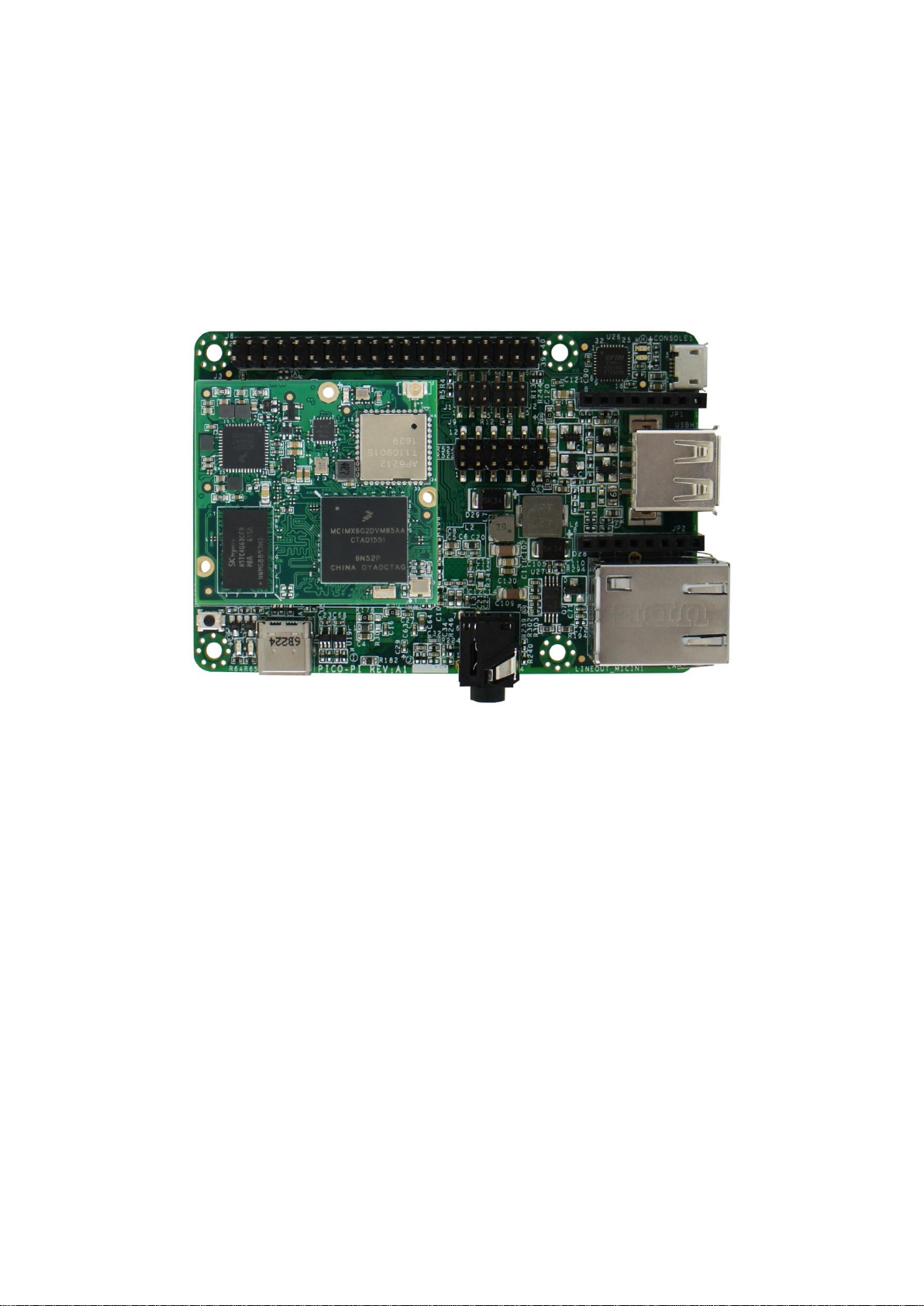
The PICO-PI-IMX6UL is a 2 board developm ent board consisting of a System -on-Module and a
carrier baseboard and optim ized for the Internet-of-Things (IoT).
Product operating temperature 60 C.
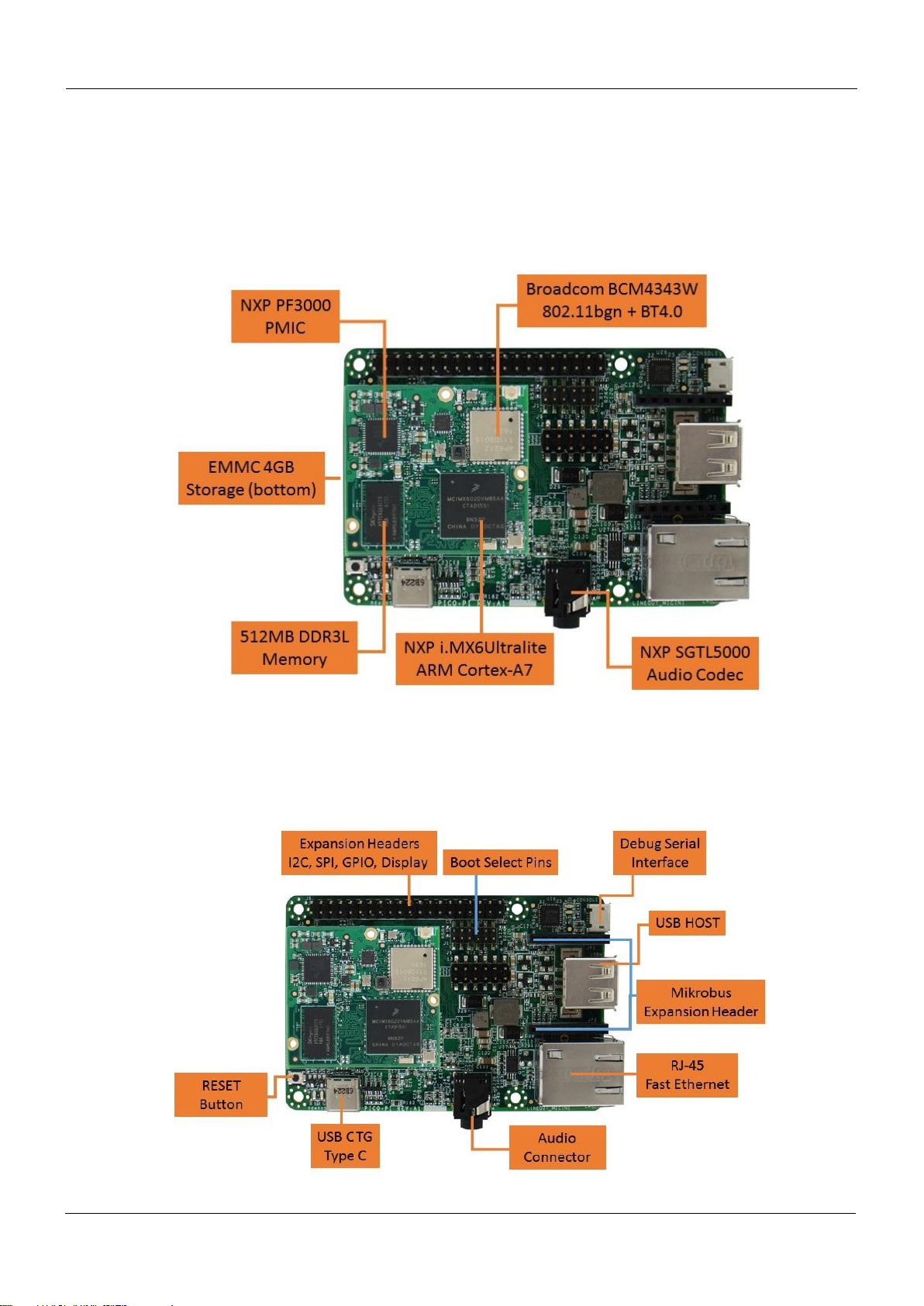
Figure 1 - PICO-PI-IM X6UL IC Identification and Overview
Figure 2 - PICO-PI-IMX6UL Connector Overview
Page 4

PICO-PI-IMX6UL HARDWARE MANUAL – VER 1.00 – FEB 24 2017
(PMIC) and WiFi / Bluetooth on the
module.
Figure 3 – PICO-PI-IMX6UL Bottom Side Connector Overview
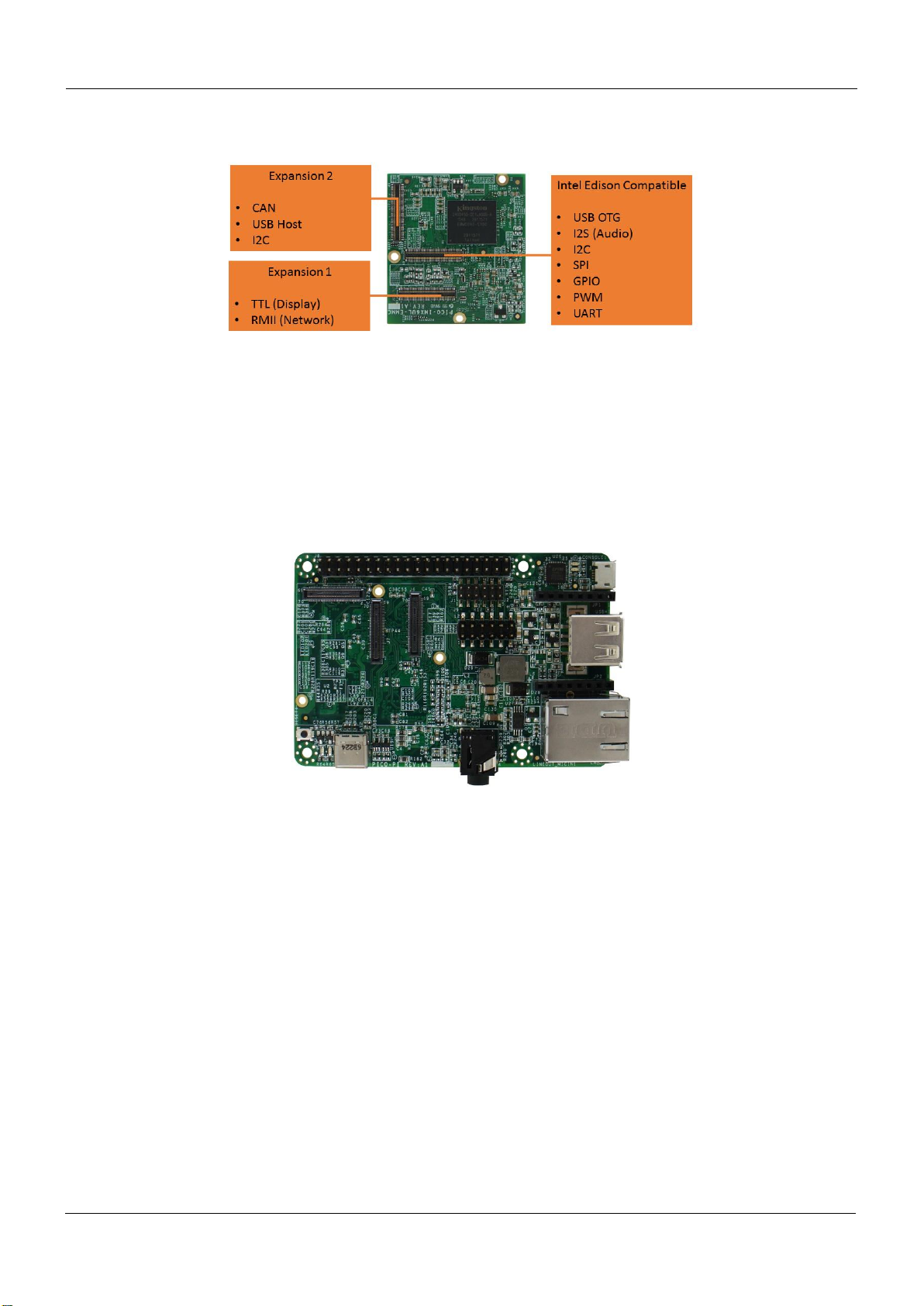
1.1. PICO-IMX6 System-on-Module Overview
The PICO-IMX6 System-on-Module (PICO-IMX6UL-EMMC) has 3 Hirose high-speed 70 pin boardto-board connectors and integrates the NXP i.MX6Ultralite, Memory, eMMC, Power Management IC
Figure 4 - PICO-IMX6 System-on-Module
Page 4 of 44
Page 5
PICO-PI-IMX6UL HARDWARE MANUAL – VER 1.00 – FEB 24 2017
Page 5 of 44
Figure 5 - PICO-IM X6 System-on-M odule Signal Overview
1.2. PICO-PI-IMX6UL Carrier Baseboard Overview
The PICO-PI-IMX6UL Carrier Baseboard (PICO-PI-FL) has 3 Hirose high-speed 70 pin board-toboard connectors that connect to the System-on-Module and provides the real-world interfaces such
as audio, network, USB and a large number of signals on the various pin headers.
Figure 6 - PICO-PI-FL Carrier Board
Page 6
PICO-PI-IMX6UL HARDWARE MANUAL – VER 1.00 – FEB 24 2017
Page 6 of 44
2. Core Components
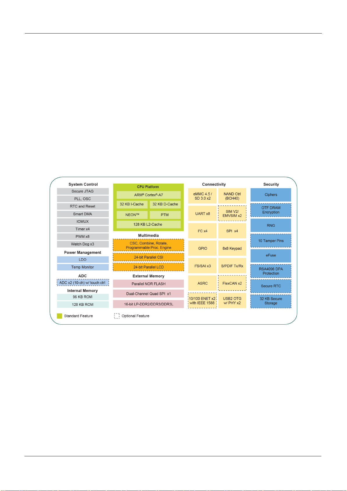
2.1. NXP i.MX6Ultralite Cortex-A7 Processor
The i.MX 6UltraLite is an ultra-efficient processor family with featuring Freescale’s advanced
implementation of the single ARM Cortex®-A7 core, which operates at speeds of up to 528 MHz.
The device is composed of the following major subsystems:
o Single-core ARM Cortex-A7 MPCore™ Platform
o 32 KBytes L1 Instruction Cache
o 32 KBytes L1 Data Cache
o Private Timer and Watchdog
o TrustZone support
o Cortex-A7 NEON MPE (Media Processing Engine) Co-processor
PXP—PiXel Processing Pipeline for imagine resize, rotation, overlay and CSC. Offloading key
pixel processing operations are required to support the LCD display applications.
Figure 7 - NXP i.MX6Ultralite Processor Blocks
Page 7
PICO-PI-IMX6UL HARDWARE MANUAL – VER 1.00 – FEB 24 2017
Page 7 of 44
2.2. NXP PF3000 Power Management IC (PMIC)
The PICO-IMX6 has on onboard NXP PF3000 power m anagem ent integrated circuit (PMIC) that
features a configurable architecture supporting the numerous outputs with various current ratings as
well as programm able voltage and sequencing required b y the com ponents on the PICO-IMX6Compute Module.
To perform a hard-reset of the PICO-IMX6 a software reset signal can be im plem ented.
CPU
BALL
CPU PAD
NAME
Pinmux (mode)
Signal
V
I/O
Description
E9
LCD_RESET
lcdif.RESET
(mode0)
RESET
3V3
I
Connected to the
PWRON signal of PMIC
The PICO-IMX6 Com pute Module as well has an RESET signal routed on connector E1_36 this
pin is connected to the RESET Button on the PICO-PI-IMX6UL. Simply pressing this button will
RESET the PICO-PI-IMX6.
Connector
Signal
V
I/O
Description
E1_36
RESET
3V3
I
Connected to the PWRON signal of PMIC on the PICO
Compute Module.
Connected to the RESET Button on the PICO-PIIMX6UL.
Figure 8 – PICO-PI-IMX6UL Reset Button Location
Page 8

PICO-PI-IMX6UL HARDWARE MANUAL – VER 1.00 – FEB 24 2017
Page 8 of 44
2.3. Memory (SKHynix)
The PICO-IMX6 integrates 512MB (4Gbit) Double Data Rate III (DDR3) S ynchronous DRAM in a
single (16 bit) channel configuration.
SK Hynix 4Gbit low power Double Data Rate III (DDR3L) Synchronous DRAM, ideally suited for the
main memory applications which requires large memory density, high bandwidth and low power
operation at 1.35V.
More information can be retrieved from SKHynix.
2.4. eMMC Storage (Kingston)
The PICO-IMX6 onboard 4GB eMMC device is connected on the SD1 pins of the i.MX6Ultralite
processor in an 8 bit width configuration.
Kingston e•MMC™ products follow the JEDEC e•MMC™ 4.5 standard. It is an ideal universal storage
solutions for many electronic devices, including smartphones, tablet PCs, PDAs, eBook readers,
digital cameras, recorders, MP3, MP4 players, electronic learning products, digital TVs and set-top
boxes. E•MMC™ encloses the MLC NAND and e•MMC™ controller inside as one JEDEC standard
package, providing a standard interface to the host. The e•MMC™ controller directly manages NAND
flash, including ECC, wear-leveling, IOPS optimization and read sensing.
The Kingston NAND Device is fully compatible with the JEDEC Standard Specification No.JESD84B45.
More information can be retrieved from Kingston.
Page 9

PICO-PI-IMX6UL HARDWARE MANUAL – VER 1.00 – FEB 24 2017
Page 9 of 44
2.5. Broadcom BCM4343W WiFi/Bluetooth SiP Module
The PICO-IMX6 com es with an onboard W iFI/Bluetooth SIP m odule. T he 802.11bgn + BT SiP
module is a small sized BGA mounted module that provides full function of 802.11bgn and Bluetooth
class 4.0 +HS
The small size & low profile physical design make it easier for system design to enable high
performance wireless connectivity without space constrain. The low power consumption and excellent
radio performance make it the best solution for OEM customers who require embedded Wi-Fi +
Bluetooth features.
The SIP module is based on Broadcom BCM4343W chipset which is a WiFi + BT SOC. The Radio
architecture & high integration MAC/BB chip provide excellent sensitivity with rich system
performance.
In addition to WEP 64/128, WPA and TKIP, AES, CCX is supported to provide the latest security
requirement on your network.
The SiP module is designed to operate with a single antenna for WiFi and Bluetooth to be connected
to the u.FL connector (separate purchase, SKU: “WBANTENNAKIT”)
Figure 9 - PICO-PI-IMX6UL WiFi / Bluetooth Module and Antenna Connector Location
Page 10

PICO-PI-IMX6UL HARDWARE MANUAL – VER 1.00 – FEB 24 2017
Page 10 of 44
Table 1 - WiFi Signal Description
CPU
BALL
PAD NAME
Pinmux
(mode)
Signal
I/O
Description
D7
NAND_DATA00
usdhc2.DATA0
(mode1)
SDIO_D0
I/O
MMC/SDIO Data bit 0
B7
NAND_DATA01
usdhc2.DATA1
(mode1)
SDIO_D1
I/O
MMC/SDIO Data bit 1
A7
NAND_DATA02
usdhc2.DATA2
(mode1)
SDIO_D2
I/O
MMC/SDIO Data bit 2
D6
NAND_DATA03
usdhc2.DATA3
(mode1)
SDIO_D3
I/O
MMC/SDIO Data bit 3
C8
NAND_WE_B
usdhc2.CMD
(mode1)
SDIO_CMD
I/O
MMC/SDIO Command
D8
NAND_RE_B
usdhc2.CLK
(mode1)
SDIO_CLK
I/O
MMC/SDIO Clock
C6
NAND_DATA04
gpio4.IO[6]
(mode5)
WL_HOST_WAKE
O
General purpose interface
pin. This pin is highimpedance on power up
and reset. Subsequently, it
becomes an input or output
through software control.
This pin has a
programmable weak pullup/down.
A6
NAND_DATA06
gpio4.IO[8]
(mode5)
WL_REG_ON
I
Used by PMU (OR-gated
with BT_REG_ON) to
power up or power down
internal BCM4339
regulators used by the
WLAN section. This pin is
also a low-asserting reset
for WLAN only
(Bluetooth is not affected
by this pin).
Page 11

PICO-PI-IMX6UL HARDWARE MANUAL – VER 1.00 – FEB 24 2017
Page 11 of 44
Table 2 - Bluetooth Signal Description
CPU
BALL
PAD NAME
Pinmux
(mode)
Signal
I/O
Description
M16
GPIO1_IO04
uart5.TX
(mode8)
BT_UART_RXD
I
Bluetooth UART Serial
Input. Serial data input for
the HCI UART Interface
M17
GPIO1_IO05
uart5.RX
(mode8)
BT_UART_TXD
O
Bluetooth UART Serial
Output. Serial data output
for the HCI UART
Interface.
M15
GPIO1_IO09
uart5.CTS_B
(mode8)
BT_UART_CTS
I/O
Bluetooth UART Clear to
Send. Active-low clear-tosend signal for the HCI
UART interface.
N17
GPIO1_IO08
uart5.RTS_B
(mode8)
BT_UART_RTS
I/O
Bluetooth UART Request
to Send. Active-low
request-to-send signal for
the HCI UART interface.
N14
JTAG_TRST_B
sai2.TX_DATA
(mode2)
BT_PCM_IN
I
PCM data input
M14
JTAG_TCK
sai2.RX_DATA
(mode2)
BT_PCM_OUT
O
PCM data output
N16
JTAG_TDI
sai2.TX_BCLK
(mode2)
BT_PCM_CLK
I/O
PCM clock
N15
JTAG_TDO
sai2.TX_SYNC
(mode2)
BT_PCB_SYNC
I/O
PCM sync signal
N9
SNVS_TAMPER8
gpio5.IO[8]
(mode5)
BT_WAKE
I
Bluetooth device wake-up:
Signal from the host to the
module indicating that the
host requires attention.
• Asserted: Bluetooth
device must wake-up or
remain awake.
• Deserted: Bluetooth
device may sleep when
sleep criteria are met.
The polarity of this signal
is software configurable
and can be asserted high
or low.
R6
SNVS_TAMPER9
gpio5.IO[9]
(mode5)
BT_RST_N
I
Low asserting reset for BT
core
B6
NAND_DATA05
gpio4.IO[7]
(mode5)
BT_HOST_WAKE
O
Host UART wake up.
Signal from the module to
the host indicating that the
module requires Attention.
• Asserted: Host device
must wake-up or remain
awake.
• Deserted: Host device
may sleep when sleep
criteria are met.
The polarity of this signal
is software configurable
and can be asserted high
or low.
Page 12
PICO-PI-IMX6UL HARDWARE MANUAL – VER 1.00 – FEB 24 2017
Page 12 of 44
3. PICO-PI-IMX6UL Interfaces and Connectors
3.1. Power Input Connector
The PICO-PI-IMX6UL can be easil y powered over the USB T ype -C cable. Operating Voltage:5Vdc
Figure 10 – PICO-PI-IMX6UL USB Type-C Location
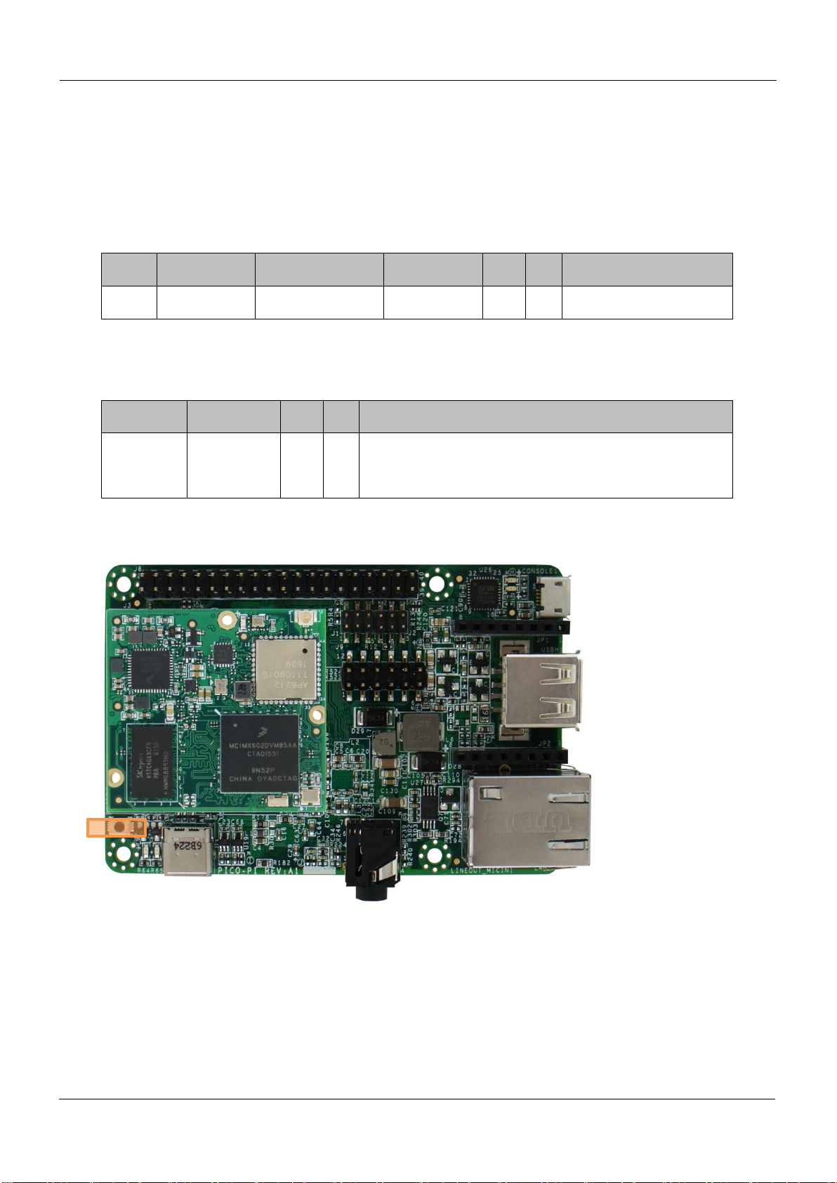
3.2. System RESET Button
Figure 11 – PICO-PI-IMX6UL Reset Button Location
Page 13
PICO-PI-IMX6UL HARDWARE MANUAL – VER 1.00 – FEB 24 2017
Page 13 of 44
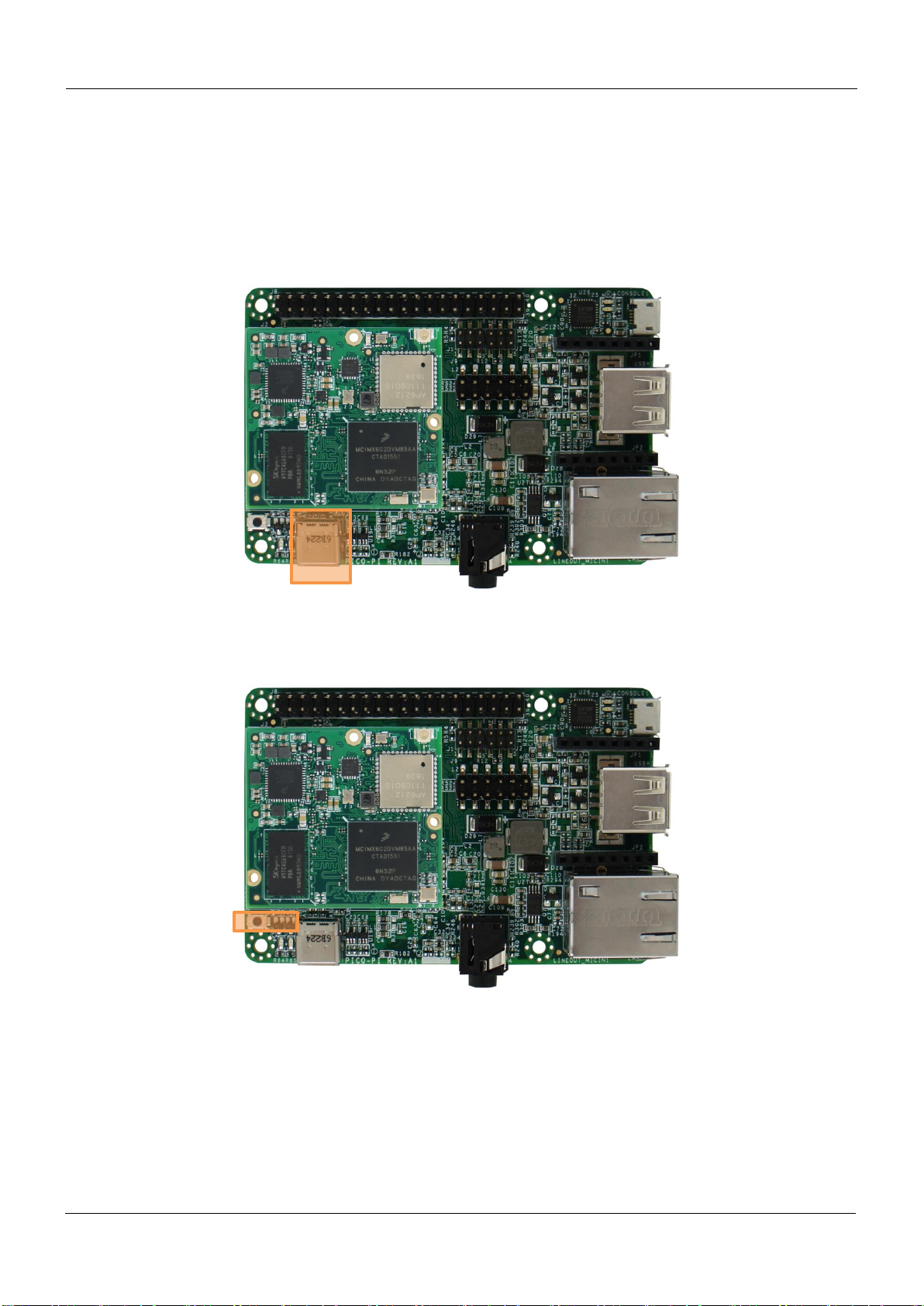
3.3. Fast Ethernet
The PICO-PI-IMX6UL features a 10/100 Mbit/s Fast Ethernet MAC compliant with the IEEE802.32002 standard. The MAC layer provides compatibility with half- or full-duplex 10/100 Mbit/s Ethernet
LANs.
Figure 12 - PICO-PI-IMX6UL RJ-45 Network Connector Location
Page 14
PICO-PI-IMX6UL HARDWARE MANUAL – VER 1.00 – FEB 24 2017
Page 14 of 44
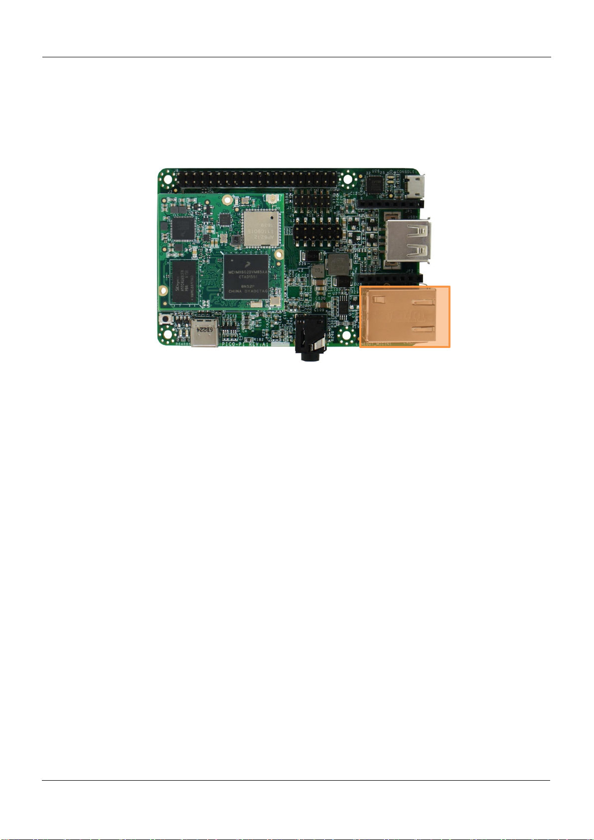
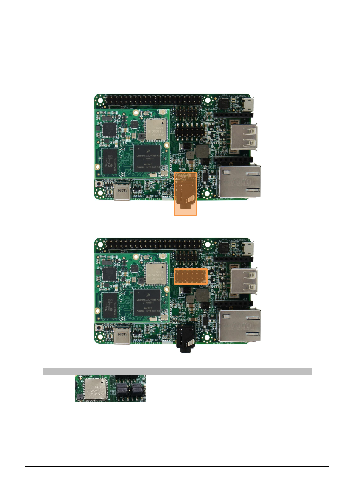
3.4. Audio Interface
The PICO-PI-IMX6UL comes with an Audio jack which is compliant with the CTIA standard. A
standard mobile phone headset will work.
Figure 13 - PICO-PI-IMX6UL Audio Jack Location
Figure 14 - PICO-PI-IMX6UL Audio I2S Signal Location
Detail
Description
Since the PICO-PI-MX6UL only has a single I2S
channel.
Please select the jumpers as the picture.
Page 15

PICO-PI-IMX6UL HARDWARE MANUAL – VER 1.00 – FEB 24 2017
Page 15 of 44
3.5. Universal Serial Bus (USB) Host Interface
The PICO-PI-IMX6UL features a standard USB 2.0 Host Connector.
Figure 15 - PICO-PI-IMX6UL USB HOST Connector Location
3.6. Universal Serial Bus (USB) OTG Interface
The PICO-PI-IMX6UL incorporates a single USB Host/OTG controller which also function as the
system power input.
The signals are routed to a USB Type-C connector.
Figure 16- PICO-PI-IMX6UL USB OTG Type-C Connector Location
Page 16

PICO-PI-IMX6UL HARDWARE MANUAL – VER 1.00 – FEB 24 2017
Page 16 of 44
3.7. Debug Interface
The PICO-PI-IMX6UL serial debug interface can be easily connected with a micro-USB cable.
The debug interface can be found on the PICO-PI-IMX6UL at the following physical location and in
software can be accessed over UART6.
Figure 17 – PICO-PI-IMX6UL Serial Debug Location
Page 17

PICO-PI-IMX6UL HARDWARE MANUAL – VER 1.00 – FEB 24 2017
Page 17 of 44
3.8. Serial Boot or eMMC Boot Control Pins
The PICO-PI-IMX6UL has a number of pins to override the default boot media (eMMC) and enter in
Serial Boot Loader mode.
Figure 18 - PICO-PI-IMX6UL Boot Control Pins
Boot from eMMC
Serial Boot Loader
Page 18

PICO-PI-IMX6UL HARDWARE MANUAL – VER 1.00 – FEB 24 2017
Page 18 of 44
3.9. Expansion Header Pins
The PICO-PI-IMX6UL has a number of expansion headers that can be used to connect sensors,
motors, and external devices.
Figure 19 - PICO-PI-IMX6UL Mikrobus Header Location
PIN
i.MX6UL
CPU PAD NAME
Signal
V
I/O
Description
JP1_1
NC
Not Connected
JP1_2
PMIC
RESET
RESET
3V3
I
Reset power signal
JP1_3
NC
Not Connected
JP1_4
J16
UART2_RXD
ECSPI3_SCLK
3V3
O
Serial Peripheral
Interface clock signal
JP1_5
J15
UART2_RTS
ECSPI3_MISO
3V3
I
Serial Peripheral
Interface master input
slave output signal
JP1_6
H14
UART2_CTS
ECSPI3_MOSI
3V3
O
Serial Peripheral
Interface master output
slave input signal
JP1_7
3V3 Power
3V3
P
3V3 Power
JP1_8
GND
P Ground
PIN
i.MX6UL
CPU PAD NAME
Signal
V
I/O
Description
JP2_1
F14
ENET1_TX_CLK
PWM7_OUT
3V3
I/O
General Purpose Input
Output with PWM control
JP2_2
E4
CSI_DATA00
GPIO4_IO21
3V3
I/O
General Purpose Input
Output
JP2_3
H16
UART3_RXD
UART3_RX
3V3
I
Universal Asynchronous
Receive Transmit receive
data signal
JP2_4
H17
UART3_TXD
UART3_TXD
3V3
O
Universal Asynchronous
Receive Transmit
transmit data signal
JP2_5
F17
UART5_TXD
I2C2_SCL
3V3
I/O
I2C bus clock line
JP2_6
G13
UART5_RXD
I2C2_SDA
3V3
I/O
I2C bus data line
JP2_7
5V Power
5V
P
5V Power
JP2_8
GND
P Ground
Page 19

PICO-PI-IMX6UL HARDWARE MANUAL – VER 1.00 – FEB 24 2017
Page 19 of 44
Figure 20 - PICO-PI-IMX6UL Expansion Header Location
PIN
i.MX6UL
CPU PAD NAME
Signal
V
I/O
Description
JP8_1
3V3 Power
3V3
P
3V3 Power
JP8_2
5V Power
5V
P
5V Power
JP8_3
G13
UART5_RXD
I2C2_SDA
3V3
I/O
I2C bus data line
JP8_4
5V Power
5V
P
5V Power
JP8_5
F17
UART5_TXD
I2C2_SCL
3V3
I/O
I2C bus clock line
JP8_6
GND
P Ground
JP8_7
G14
UART3_RTS
UART3_RTS
3V3
O
Universal Asynchronous
Receive Transmit request
to send signal
JP8_8
H17
UART3_TXD
UART3_TXD
3V3
O
Universal Asynchronous
Receive Transmit
transmit data signal
JP8_9
GND
P Ground
JP8_10
H16
UART3_RXD
UART3_RXD
3V3
I
Universal Asynchronous
Receive Transmit receive
data signal
JP8_11
F14
ENET1_TX_CLK
PWM7_OUT
3V3
I/O
General Purpose Input
Output with PWM control
JP8_12
H15
UART3_CTS
UART3_CTS
3V3
O
Universal Asynchronous
Receive Transmit clear to
send signal
JP8_13
D15
ENET1_RX_ER
PWM8_OUT
3V3
I/O
General Purpose Input
Output with PWM control
JP8_14
GND
P Ground
JP8_15
NC
Not Connected
JP8_16
F16
ENET1_RXD0
CAN1_TX
3V3
I/O
CAN (controller Area
Network) transmit signal
JP8_17
3V3 Power
3V3
P
3V3 Power
JP8_18
E17
ENET1_RXD1
CAN1_RX
3V3
I/O
CAN (controller Area
Network) receive signal
JP8_19
H14
UART2_CTS
ECSPI3_MOSI
3V3
O
Serial Peripheral
Interface
master output slave input
signal
JP8_20
GND
P Ground
Page 20

PICO-PI-IMX6UL HARDWARE MANUAL – VER 1.00 – FEB 24 2017
Page 20 of 44
JP8_21
J15
UART2_RTS
ECSPI3_MISO
3V3
I
Serial Peripheral
Interface
master input slave output
signal
JP8_22
NC
Not Connected
JP8_23
J16
UART2_RXD
ECSPI3_SCLK
3V3
O
Serial Peripheral
Interface
clock signal
JP8_24
NC
Not Connected
JP8_25
GND
P Ground
JP8_26
J17
UART2_TXD
ECSPI3_SS0
3V3
I/O
Serial Peripheral
Interface
Chip Select 1 signal
JP8_27
K16
UART1_RXD
I2C3_SDA
3V3
I/O
I2C bus data line
JP8_28
K14
UART1_TXD
I2C3_SCL
3V3
I/O
I2C bus clock line
JP8_29
E4
CSI_DATA00
GPIO4_IO21
3V3
I/O
General Purpose Input
Output
JP8_30
GND
P Ground
JP8_31
E3
CSI_DATA01
GPIO4_IO22
3V3
I/O
General Purpose Input
Output
JP8_32
E1
CSI_DATA03
GPIO4_IO24
3V3
I/O
General Purpose Input
Output
JP8_33
E2
CSI_DATA02
GPIO4_IO23
3V3
I/O
General Purpose Input
Output
JP8_34
GND
P Ground
JP8_35
F2
CSI_VSYNC
GPIO4_IO19
3V3
I/O
General Purpose Input
Output
JP8_36
P11
SNVS_TAMPER2
GPIO5_IO02
3V3
I/O
General Purpose Input
Output
JP8_37
K15
UART1_CTS
GPIO4_IO18
3V3
I/O
General Purpose Input
Output
JP8_38
E16
ENET1_RX_EN
CAN2_TX
3V3
I/O
CAN (controller Area
Network) transmit signal
JP8_39
GND
P Ground
JP8_40
E15
ENET1_TXD0
CAN2_RX
3V3
I/O
CAN (controller Area
Network) receive signal
Page 21

PICO-PI-IMX6UL HARDWARE MANUAL – VER 1.00 – FEB 24 2017
Page 21 of 44
3.10. Display and Touch Connector
The PICO-PI-IMX6UL features a Touch and RGB TTL Display interface that can be connected directly
to a multi-touch 24-bit LCD panel.
The following LCD displays have been tested:
Manufacturer
Partnumber
Description
TechNexion
TDP0500T800480PCAP
5 INCH 800 x 480 PCAP MULTI TOUCH LCD
PANEL INCLUDING TOUCH CABLE
TechNexion
TDP0700T800480PCAP
7 INCH 800 x 480 PCAP MULTI TOUCH LCD
PANEL INCLUDING TOUCH CABLE
5 INCH
7 INCH
1 – 8 : ON
2 – 7 : OFF
3 – 6 : ON
4 – 5 : OFF
1 – 8 : ON
2 – 7 : ON
3 – 6 : ON
4 – 5 : OFF
Figure 21 - PICO-PI-IMX6UL LCD Display FPC Connector Location
Page 22

PICO-PI-IMX6UL HARDWARE MANUAL – VER 1.00 – FEB 24 2017
Page 22 of 44
PIN
i.MX6UL
CPU PAD NAME
Signal
V
I/O
Description
LCD1_1
VLED+
21V7
LED Backlight Voltage
LCD1_2
VLED+
21V7
LED Backlight Voltage
LCD1_3
VLED-
GND
P
Ground
LCD1_4
VLED-
GND
P
Ground
LCD1_5
GND
P Ground
LCD1_6
VCOM
4V09
Common Voltage
LCD1_7
DVDD
3V3
Power for Digital Circuit
LCD1_8
MODE
3V3
DE/SYNC mode select
LCD1_9
B8
LCD_ENABLE
LCDIF_ENABLE
3V3
O
LCD dot enable pin
signal
LCD1_10
C9
LCD_VSYNC
LCDIF_VSYNC
3V3
O
LCD Vertical
Synchronization
LCD1_11
D9
LCD_HSYNC
LCDIF_HSYNC
3V3
O
LCD Horizontal
Synchronization
LCD1_12
D11
LCD_DATA7
LCDIF_DATA7
3V3
O
LCD Pixel Data bit 7
LCD1_13
A10
LCD_DATA6
LCDIF_DATA6
3V3
O
LCD Pixel Data bit 6
LCD1_14
B10
LCD_DATA5
LCDIF_DATA5
3V3
O
LCD Pixel Data bit 5
LCD1_15
C10
LCD_DATA4
LCDIF_DATA4
3V3
O
LCD Pixel Data bit 4
LCD1_16
D10
LCD_DATA3
LCDIF_DATA3
3V3
O
LCD Pixel Data bit 3
LCD1_17
E10
LCD_DATA2
LCDIF_DATA2
3V3
O
LCD Pixel Data bit 2
LCD1_18
A9
LCD_DATA1
LCDIF_DATA1
3V3
O
LCD Pixel Data bit 1
LCD1_19
B9
LCD_DATA0
LCDIF_DATA0
3V3
O
LCD Pixel Data bit 0
LCD1_20
D13
LCD_DATA15
LCDIF_DATA15
3V3
O
LCD Pixel Data bit 15
LCD1_21
A12
LCD_DATA14
LCDIF_DATA14
3V3
O
LCD Pixel Data bit 14
LCD1_22
B12
LCD_DATA13
LCDIF_DATA13
3V3
O
LCD Pixel Data bit 13
LCD1_23
C12
LCD_DATA12
LCDIF_DATA12
3V3
O
LCD Pixel Data bit 12
LCD1_24
D12
LCD_DATA11
LCDIF_DATA11
3V3
O
LCD Pixel Data bit 11
LCD1_25
E12
LCD_DATA10
LCDIF_DATA10
3V3
O
LCD Pixel Data bit 10
LCD1_26
A11
LCD_DATA9
LCDIF_DATA9
3V3
O
LCD Pixel Data bit 9
LCD1_27
B11
LCD_DATA8
LCDIF_DATA8
3V3
O
LCD Pixel Data bit 8
LCD1_28
B16
LCD_DATA23
LCDIF_DATA23
3V3
O
LCD Pixel Data bit 23
LCD1_29
A14
LCD_DATA22
LCDIF_DATA22
3V3
O
LCD Pixel Data bit 22
LCD1_30
B14
LCD_DATA21
LCDIF_DATA21
3V3
O
LCD Pixel Data bit 21
LCD1_31
C14
LCD_DATA20
LCDIF_DATA20
3V3
O
LCD Pixel Data bit 20
LCD1_32
D14
LCD_DATA19
LCDIF_DATA19
3V3
O
LCD Pixel Data bit 19
LCD1_33
A13
LCD_DATA18
LCDIF_DATA18
3V3
O
LCD Pixel Data bit 18
LCD1_34
B13
LCD_DATA17
LCDIF_DATA17
3V3
O
LCD Pixel Data bit 17
LCD1_35
C13
LCD_DATA16
LCDIF_DATA16
3V3
O
LCD Pixel Data bit 16
LCD1_36
GND
P Ground
LCD1_37
A8
LCD_CLK
LCDIF_CLK
3V3
O
LCD Pixel Clock
LCD1_38
GND
P Ground
LCD1_39
L/R
3V3
I
Left / Right Selection
LCD1_40
U/D
3V3
I
Up / Down Selection
LCD1_41
VGH
16V0
P
Gate ON Voltage
LCD1_42
VGL
-6V0
P
Gate OFF Voltage
LCD1_43
AVDD
10V4
P
Power for Analog Circuit
LCD1_44
RESET
RESET
3V3
I
Reset power signal
LCD1_45
NC
Not Connected
LCD1_46
VCOM
3V3
I
Common voltage
LCD1_47
DITHB
3V3
I
Dithering function
LCD1_48
GND
P Ground
LCD1_49
NC
Not Connected
LCD1_50
NC
Not Connected
Page 23

PICO-PI-IMX6UL HARDWARE MANUAL – VER 1.00 – FEB 24 2017
Page 23 of 44
Figure 22 - PICO-PI-IMX6UL Touch Panel Connector Location
PIN
i.MX6UL
CPU PAD NAME
Signal
V
I/O
Description
TOUCH_1
L17
GPIO1_IO03
I2C1_SDA
3V3
I/O
I2C bus data line
TOUCH_2
L14
GPIO1_IO02
I2C1_SCL
3V3
I/O
I2C bus clock line
TOUCH_3
3V3 Power
3V3
P
3V3 Power
TOUCH_4
G16
UART4_RXD
GPIO4_IO29
3V3
I/O
General Purpose Input
Output
TOUCH_5
E1
CSI_DATA03
GPIO4_IO24
3V3
I/O
General Purpose Input
Output
TOUCH_6
GND
P Ground
Page 24

PICO-PI-IMX6UL HARDWARE MANUAL – VER 1.00 – FEB 24 2017
Page 24 of 44
4. Booting up the PICO-PI-IMX6UL
4.1.1. Overview
The boot mode for the PICO-PI-IMX6UL is controlled with jumpers on the baseboard. Normally, the
board is intended to boot from the on-board eMMC flash, but sometimes the board needs to be
booted from an external source. This can happen for example if the eMMC contains a faulty
bootloader. This document guides how the on-board eMMC flash of a PICO-PI-IMX6UL can be
flashed from a host PC.
4.1.2 i.MX6UL boot process details
When the boot jumpers are set to eMMC boot, the ROM code will attempt to boot from eMMC. If there
is no bootable software present, the board will revert to "serial download mode". The name "serial
download mode" is slighlty misleading, since the mode has grown past UART communication and
nowadays is a way to access the board over an USB OTG port, or in the case of PICO-PI-IMX6UL,
the USB type C port.
4.1.3 Changing PICO-PI-IMX6UL boot mode
To force the board into serial download mode using a PICO-PI-IMX6UL, change the boot mode
jumpers J1 to 1-2 and jumper J4 to 2-3, as pictured below.
With this jumper setting, the board will not even attempt to boot from eMMC, but always expect it to
be programmed over the USB type C connector.
To set the boot mode to eMMC, restore the jumpers J1 to 2-3 and jumper J4 to 1-2 (as pictured
below).
Page 25

PICO-PI-IMX6UL HARDWARE MANUAL – VER 1.00 – FEB 24 2017
Page 25 of 44
In this mode the board will attempt to boot from eMMC, but can in some circumstances revert to serial
download mode. This can happen for instance if the eMMC is not bootable. Note that "half-booting"
software, like a u-boot that does not initialize memory timings for correct operation, will be interpreted
as booting. More technically, if the ROM code finds the correct signature 1kB into the eMMC, it
considers the board bootable from eMMC. To verify your PICO-PI-IMX6UL is in serial download
mode, connect a USB cable between the host PC and the PICO-PI-IMX6UL. Power up the board. If a
USB device with name "Freescale Semiconductor in Recovery Mode" appears, the board is in serial
download mode.
Page 26

PICO-PI-IMX6UL HARDWARE MANUAL – VER 1.00 – FEB 24 2017
Page 26 of 44
4.1.4 Preparing a bootable software image
This section explains how software should be laid out inside the eMMC for a succesful boot. There
are also steps how to prepare software to be programmed into the PICO-PI-IMX6UL eMMC.
4.1.4.1 Procedure overview
The procedure recommended here for programming the board is:
1. Prepare a file containing a bit-by-bit copy of what should be in eMMC (an "image" file). The
layout of such files is described in sections 4.1.4.2 and 4.1.4.3.
2. Booting the board in serial download mode
3. Accessing the eMMC as a mass storage device (see chapters 4.2 and 4.3)
4. Copying the eMMC image file to the board
5. Booting the image
4.1.4.2 eMMC boot overview
This section describes how to use a Linux computer to prepare an image file of eMMC content. This
step can be omitted, but is useful for creating image files which are easily distributable (since it is a
all-in-one file).
A conventional Linux image consists of
u-boot bootloader
kernel
devicetree
root filesystem
and sometimes, an initial ramdisk
The usual set up is that the kernel, device tree and the optional RAM disk is placed in a FAT partition
as the first partition, and the OS filesystems occupies the remaining partitions. Linux systems usually
occupy just the second partition, and in case a swap partition, also the third partition, but other
operating systems can make use of more advanced partition schemes.
Convenient ways to prepare an image using a Linux computer is using a block device (like a USB
stick or an SD card) or a loopback device. It is also possible to access the eMMC as a mass storage
device and manually place the data in the right place. See section 4.3.x.
4.1.4.3 Preparing an OS image
This section describes how to prepare the eMMC contents so the system can boot. This is intended
for those wanting to prepare their own image, and not to use an image already provided by someone
else.
The device is assumed to be a block device (like USB stick or SD card), but can beneficially be the
eMMC itself (see chapter 4.2 and 4.3 on how to access the eMMC as a block device on a host PC).
Here the block device is denoted /dev/sdX; care must be taken that the right device is used.
First, partition your device. Leave the first 1MB (or so) unpartitioned so that the first partition starts
about 1MB into the device. The reason for this is that the u-boot bootloader needs to reside in
unpartitioned space in the beginning of the block device.
The first partition is usually a FAT partition containing the Linux kernel as a zImage and the device
tree blob (dtb) file. If an initial ramdisk is used, the initrd files can also reside in the FAT partition.
The second partition is usually the Linux root file system. Keep in mind when partitioning that the
eMMC is limited in size to approximately 4GB, and not let your image become too large to fit.
Page 27

PICO-PI-IMX6UL HARDWARE MANUAL – VER 1.00 – FEB 24 2017
Page 27 of 44
Then copy your bootloader (u-boot) 1kB into the image. On a Linux host, the following command can
be used. Remember to replace /dev/sdX with the appropriate device or image file.
# dd if=u-boot.imx of=/dev/sdX bs=1k seek=1 conv=notrunc oflag=dsync
Thereafter format the additional partitions, with the expected file systems, copy the files there.
4.1.4.4 Creating the image file from a block device
As a last step create the image file from your block device. This can be done using the following Linux
commands: First list the partitions in the block device:
# fdisk -lc /dev/sdX
The output looks something like:
Disk /dev/sdX: 3965 MB, 3965190144 bytes
122 heads, 62 sectors/track, 1023 cylinders
Units = cylinders of 7564 * 512 = 3872768 bytes
Sector size (logical/physical): 512 bytes / 512 bytes
I/O size (minimum/optimal): 512 bytes / 512 bytes
Disk identifier: 0x0005ffff
Device Boot Start End Blocks Id System
/dev/sdX1 2 4 8192+ 83 FAT12
/dev/sdX2 4 85 307200 83 Linux
/dev/sdX3 85 363 1048576 82 Linux swap
To extract the OS image from this issue the command
# dd if=/dev/sdX of=image.img bs=3872768 count=85
The blocksize (bs= parameter) is taken from the line "Units = cylinders of 7564 * 512 = 3872768
bytes" and the count parameter is the end of the last non-swap partition, /dev/sdX2.
Page 28

PICO-PI-IMX6UL HARDWARE MANUAL – VER 1.00 – FEB 24 2017
Page 28 of 44
4.2. Programming PICO-PI-IMX6UL using a Windows host
This section guides on how to use a Windows 7 computer to access the eMMC on a PICO-PIIMX6UL, and how to program an image file to the eMMC.
Tools needed:
sb_loader_imx6ul.exe (or similar)
a "bootbomb" file that can be dropped on the board, enabling it to be accessible as a USB
Mass Storage device
Windiskimager or similar tool that allows raw writing of block devices.
An eMMC image file to be programmed to the eMMC flash of the board.
And optionally, a serial terminal emulator program
For convenience, there is a downloadable tool package containing the three first items at:
http://www.wandboard.org/downloads/hobbit/hobbitboard_tools-20160322.zip
4.2.1. Preparing the setup
First attach a USB Type C peripheral cable to the board, and the other end to the host PC. Set the
boot jumpers to serial download mode, power up the board, and verify that a "SE Blank 6UL" device
appears (as below):
Next, download the tools package. Copy the folder inside the ZIP file to the Desktop.
Page 29

PICO-PI-IMX6UL HARDWARE MANUAL – VER 1.00 – FEB 24 2017
Page 29 of 44
4.2.2. Using sb_loader
Then start a command prompt by clicking on the start menu, and in the "Search programs and files"
box enter "cmd" (see below):
In the command line interface, navigate to the PICO-PI-IMX6UL tools package and the sb_loader
folder inside it by typing the following commands:
cd Desktop
cd hobbitboard_tools-20160322
cd windows
cd sb_loader
(see screenshot below)
Page 30

PICO-PI-IMX6UL HARDWARE MANUAL – VER 1.00 – FEB 24 2017
Page 30 of 44
Next run sb_loader to boot the image on the board. Issue the command:
sb_loader_imx6ul.exe -f ..\..\bootbomb-20160306.imx
The loader will push the image to the board, and a mass storage device will appear (in the example
below it gets the letter F:)
Page 31

PICO-PI-IMX6UL HARDWARE MANUAL – VER 1.00 – FEB 24 2017
Page 31 of 44
4.2.3. Using WinDiskImager to flash the eMMC
Start win32diskimager, and open the image file that is to be used. In the image below the file picoimx6ul-buildroot-2016030.img is used as an example.
NOTE: It is important that you use the mass storage device that appeared when using sb_loader,
using the wrong device might corrupt your hard drive!
After WinDiskImager finishes, power off the board, set the boot jumpers back to eMMC boot and
power up the board.
Page 32

PICO-PI-IMX6UL HARDWARE MANUAL – VER 1.00 – FEB 24 2017
Page 32 of 44
4.3. Programming PICO-PI-IMX6UL eMMC using a Linux host
This section describes how to program the eMMC using a Linux computer. The description below is
less verbose as the one for Windows systems.
Tools needed are:
imx_usb loader
a "bootbomb" file that can be dropped on the board, enabling it to be accessible as a USB
Mass Storage device
And, preferrably, an eMMC image file to be programmed to the eMMC flash of the board.
As above, the two first items are included in the tools package at:
http://www.wandboard.org/downloads/hobbit/hobbitboard_tools-20160322.zip
4.3.1. Using imx_usb tool and flashing the eMMC
Boot the board in serial download mode. Connect the USB type C cable to the board and the other
end to the host PC.
It is possible to use the command 'lsusb' to verify that the board really is in serial download mode. If
so, then there is a "Freescale Semiconductor" device present in the list:
Bus 002 Device 033: ID 15a2:007d Freescale Semiconductor, Inc.
Then drop the boot image on the board with the command
# ./imx_usb bootbomb.imx
After a few seconds a USB Mass Storage Device appears.
Now it is possilble to use commands like 'dd' to program the eMMC on the board, for instance copying
an operating system image file to the board can be done with:
# dd if=image.img of=/dev/sdX bs=1M oflag=dsync
where sdX is the mass storage device corresponding to the PICO-PI-IMX6UL EMMC.
After this, change the jumpers back to eMMC boot and reboot the board.
4.3.2. Copying files to eMMC without an image file
It is also possible to assemble an image directly in the eMMC of the PICO-PI-IMX6UL. To do so,
perform the steps in chapter 4.1.4.3 using the Mass Storage block device presented after running the
imx_usb tool.
Page 33

PICO-PI-IMX6UL HARDWARE MANUAL – VER 1.00 – FEB 24 2017
Page 33 of 44
5. PICO-IMX6 Compute M odule Pin Assignment
W ant to m ak e your own carrier baseboard and want t o use the PICO-IMX6 Com pute Module.
Here is the complete pinout.
PIN
CPU
BALL
CPU PAD NAME
Signal
V
I/O
Description
E1_1
GND
P Ground
E1_2
VSYS
P
System input power (4.0
to 5.25V)
E1_3
K13
GPIO1_IO00
USB_OTG1_PWR
3V3
I
USB OTG ID Pin
E1_4
VSYS
P
System input power (4.0
to 5.25V)
E1_5
GND
P Ground
E1_6
VSYS
P
System input power (4.0
to 5.25V)
E1_7
NC
Not Connected
E1_8
3V3 P
System 3.3V Output
E1_9
GND
P Ground
E1_10
3V3 P
System 3.3V Output
E1_11
GND
P Ground
E1_12
1V8 P
System 1.8V Output
(same as E1 connector
I/O voltage levels)
E1_13
GND
P Ground
E1_14
VSYS
P
System input power (4.0
to 5.25V)
E1_15
GND
P Ground
E1_16
U15
USB_OTG1_DP
USB_OTG_DP
USB
I/O
Universal Serial Bus
differential pair positive
signal
E1
X1
X2
Page 34

PICO-PI-IMX6UL HARDWARE MANUAL – VER 1.00 – FEB 24 2017
Page 34 of 44
PIN
CPU
BALL
CPU PAD NAME
Signal
V
I/O
Description
E1_17
R8
ONOFF
SRC_RESET_B
3V3
I
Power ON button input
signal
E1_18
T15
USB_OTG1_DN
USB_OTG1_DN
USB
I/O
Universal Serial Bus
differential pair negative
signal
E1_19
L15
GPIO1_IO01
GPIO1_IO01
1V8
I
Over current detect input
pin to monitor USB power
over current
E1_20
T12
USB_OTG1_VBUS
USB_OTG1_VBUS
5V
I/O
Universal Serial Bus
power
E1_21
K17
GPIO1_IO06
USB_OTG_
PWR_WAKE
USB
I
Universal Serial Bus
power enable
E1_22
E5
CSI_PIXCLK
UART6_RX
1V8
I
Universal Asynchronous
Receive Transmit receive
data signal
E1_23
NC
Not Connected
E1_24
F2
CSI_VSYNC
GPIO4_IO19
1V8
I/O
General Purpose Input
Output
E1_25
F3
CSI_HSYNC
GPIO4_IO20
1V8
I/O
General Purpose Input
Output
E1_26
E4
CSI_DATA00
GPIO4_IO21
1V8
I/O
General Purpose Input
Output
E1_27
F5
CSI_MCLK
UART6_TX
1V8
O
Universal Asynchronous
Receive Transmit transmit
data signal
E1_28
E3
CSI_DATA01
GPIO4_IO22
1V8
I/O
General Purpose Input
Output
E1_29
NC
Not Connected
E1_30
E2
CSI_DATA02
GPIO4_IO23
1V8
I/O
General Purpose Input
Output
E1_31
NC
Not Connected
E1_32
E1
CSI_DATA03
GPIO4_IO24
1V8
I/O
General Purpose Input
Output
E1_33
D15
ENET1_RX_ER
PWM8_OUT
1V8
I/O
General Purpose Input
Output with PWM control
E1_34
K15
UART1_CTS
GPIO4_IO18
1V8
I/O
General Purpose Input
Output
E1_35
F14
ENET1_TX_CLK
PWM7_OUT
1V8
I/O
General Purpose Input
Output with PWM control
E1_36
PMIC
RESET
RESET
1V8
I
Reset power signal
E1_37
NC
Not Connected
E1_38
NC
Not Connected
E1_39
NC
Not Connected
E1_40
NC
Not Connected
E1_41
F17
UART5_TXD
I2C2_SCL
1V8
I/O
I2C bus clock line
E1_42
G17
UART4_TXD
GPIO4_IO28
1V8
I/O
General Purpose Input
Output
E1_43
G13
UART5_RXD
I2C2_SDA
1V8
I/O
I2C bus data line
E1_44
G16
UART4_RXD
GPIO4_IO29
1V8
I/O
General Purpose Input
Output
E1_45
K14
UART1_TXD
I2C3_SCL
1V8
I/O
I2C bus clock line
Page 35

PICO-PI-IMX6UL HARDWARE MANUAL – VER 1.00 – FEB 24 2017
Page 35 of 44
PIN
CPU
BALL
CPU PAD NAME
Signal
V
I/O
Description
E1_46
H17
UART3_TXD
UART3_TXD
1V8
O
Universal Asynchronous
Receive Transmit transmit
data signal
E1_47
K16
UART1_RXD
I2C3_SDA
1V8
I/O
I2C bus data line
E1_48
P11
SNVS_TAMPER2
GPIO5_IO02
1V8
I/O
General Purpose Input
Output
E1_49
NC
Not Connected
E1_50
D2
CSI_DATA06
SAI1_RX_DATA
1V8
I
Integrated Interchip
Sound (I2S) channel
receive data line
E1_51
NC
Not Connected
E1_52
D3
CSI_DATA05
SAI1_TX_BCLK
1V8
O
Integrated Interchip
Sound (I2S) channel word
clock signal
E1_53
J17
UART2_TXD
ECSPI3_SS0
1V8
Serial Peripheral Interface
Chip Select 1 signal
E1_54
D4
CSI_DATA04
SAI1_TX_SYNC
1V8
O
Integrated Interchip
Sound (I2S) channel
frame synchronization
signal
E1_55
J16
UART2_RXD
ECSPI3_SCLK
1V8
O
Serial Peripheral Interface
clock signal
E1_56
D1
CSI_DATA07
SAI1_TX_DATA
1V8
O
Integrated Interchip
Sound (I2S) channel
transmit data line
E1_57
H14
UART2_CTS
ECSPI3_MOSI
1V8
O
Serial Peripheral Interface
master output slave input
signal
E1_58
NC
Not Connected
E1_59
J15
UART2_RTS
ECSPI3_MISO
1V8
I
Serial Peripheral Interface
master input slave output
signal
E1_60
NC
Not Connected
E1_61
H16
UART3_RXD
UART3_RX
1V8
I
Universal Asynchronous
Receive Transmit receive
data signal
E1_62
NC
Not Connected
E1_63
G14
UART3_RTS
UART3_RTS
1V8
O
Universal Asynchronous
Receive Transmit request
to send signal
E1_64
NC
Not Connected
E1_65
H15
UART3_CTS
UART3_CTS
1V8
O
Universal Asynchronous
Receive Transmit clear to
send signal
E1_66
NC
Not Connected
E1_67
NC
Not Connected
E1_68
NC
Not Connected
E1_69
NC
Not Connected
E1_70
NC
Not Connected
Page 36

PICO-PI-IMX6UL HARDWARE MANUAL – VER 1.00 – FEB 24 2017
Page 36 of 44
PIN
CPU
BALL
CPU PAD NAME
Signal
V
I/O
Description
X1_1
GND
P Ground
X1_2
GND
P Ground
X1_3
NC
Not Connected
X1_4
NC
Not Connected
X1_5
NC
Not Connected
X1_6
NC
Not Connected
X1_7
GND
P Ground
X1_8
B16
LCD_DATA23
LCDIF_DATA23
3V3
O
LCD Pixel Data bit 23
X1_9
NC
Not Connected
X1_10
A14
LCD_DATA22
LCDIF_DATA22
3V3
O
LCD Pixel Data bit 22
X1_11
NC
Not Connected
X1_12
B14
LCD_DATA21
LCDIF_DATA21
3V3
O
LCD Pixel Data bit 21
X1_13
GND
P Ground
X1_14
C14
LCD_DATA20
LCDIF_DATA20
3V3
O
LCD Pixel Data bit 20
X1_15
NC
Not Connected
X1_16
D14
LCD_DATA19
LCDIF_DATA19
3V3
O
LCD Pixel Data bit 19
X1_17
NC
Not Connected
X1_18
A13
LCD_DATA18
LCDIF_DATA18
3V3
O
LCD Pixel Data bit 18
X1_19
GND
P Ground
X1_20
B13
LCD_DATA17
LCDIF_DATA17
3V3
O
LCD Pixel Data bit 17
X1_21
NC
Not Connected
X1_22
C13
LCD_DATA16
LCDIF_DATA16
3V3
O
LCD Pixel Data bit 16
X1_23
NC
Not Connected
X1_24
D13
LCD_DATA15
LCDIF_DATA15
3V3
O
LCD Pixel Data bit 15
X1_25
GND
P Ground
X1_26
A12
LCD_DATA14
LCDIF_DATA14
3V3
O
LCD Pixel Data bit 14
X1_27
NC
Not Connected
X1_28
B12
LCD_DATA13
LCDIF_DATA13
3V3
O
LCD Pixel Data bit 13
X1_29
NC
Not Connected
X1_30
C12
LCD_DATA12
LCDIF_DATA12
3V3
O
LCD Pixel Data bit 12
X1_31
GND
P Ground
X1_32
D12
LCD_DATA11
LCDIF_DATA11
3V3
O
LCD Pixel Data bit 11
X1_33
F15
ENET1_TXEN
ENET2_MDIC
3V3
Management data clock
reference
X1_34
E12
LCD_DATA10
LCDIF_DATA10
3V3
O
LCD Pixel Data bit 10
X1_35
E14
ENET1_TXD1
ENET2_MDIO
3V3
Management data
X1_36
A11
LCD_DATA9
LCDIF_DATA9
3V3
O
LCD Pixel Data bit 9
X1_37
D16
ENET2_RXER
GPIO2_IO15
3V3
Ethernet reset
X1_38
B11
LCD_DATA8
LCDIF_DATA8
3V3
O
LCD Pixel Data bit 8
X1_39
N11
SNVS_TAMPER6
GPIO5_IO06
3V3
Ethernet interrupt output
X1_40
D11
LCD_DATA7
LCDIF_DATA7
3V3
O
LCD Pixel Data bit 7
X1_41
L16
GPIO1_IO07
ANATOP_ENET_
REF_CLK2
3V3
Synchronous Ethernet
recovered clock
X1_42
A10
LCD_DATA6
LCDIF_DATA6
3V3
O
LCD Pixel Data bit 6
X1_43
B15
ENET2_TXEN
ENET2_TX_EN
3V3
RMII transmit enable
X1_44
B10
LCD_DATA5
LCDIF_DATA5
3V3
O
LCD Pixel Data bit 5
X1_45
B17
ENET2_CRS_DV
ENET2_RX_EN
3V3
RMII receive data valid
X1_46
C10
LCD_DATA4
LCDIF_DATA4
3V3
O
LCD Pixel Data bit 4
Page 37

PICO-PI-IMX6UL HARDWARE MANUAL – VER 1.00 – FEB 24 2017
Page 37 of 44
PIN
CPU
BALL
CPU PAD NAME
Signal
V
I/O
Description
X1_47
GND
P Ground
X1_48
D10
LCD_DATA3
LCDIF_DATA3
3V3
O
LCD Pixel Data bit 3
X1_49
D17
ENET2_TXCLK
ENET2_TX_CLK
3V3
O
RMII transmit clock
X1_50
E10
LCD_DATA2
LCDIF_DATA2
3V3
O
LCD Pixel Data bit 2
X1_51
A15
ENET2_TXD0
ENET2_TX_DATA0
3V3
O
RMII transmit data 0
X1_52
A9
LCD_DATA1
LCDIF_DATA1
3V3
O
LCD Pixel Data bit 1
X1_53
A16
ENET2_TXD1
ENET2_TX_DATA1
3V3
O
RMII transmit data 1
X1_54
B9
LCD_DATA0
LCDIF_DATA0
3V3
O
LCD Pixel Data bit 0
X1_55
NC
Not Connected
X1_56
N8
SNVS_TAMPER5
GPIO5_IO05
3V3
O
LCD backlight
enable/disable
X1_57
NC
Not Connected
X1_58
D9
LCD_HSYNC
LCDIF_HSYNC
3V3
O
LCD Horizontal
Synchronization
X1_59
GND
P Ground
X1_60
B8
LCD_ENABLE
LCDIF_ENABLE
3V3
O
LCD dot enable pin
signal
X1_61
NC
Not Connected
X1_62
C9
LCD_VSYNC
LCDIF_VSYNC
3V3
O
LCD Vertical
Synchronization
X1_63
C17
ENET2_RXD0
ENET2_RX_DATA0
3V3
I
RMII receive data 0
X1_64
A8
LCD_CLK
LCDIF_CLK
3V3
O
LCD Pixel Clock
X1_65
C16
ENET2_RXD1
ENET2_RX_DATA1
3V3
I
RMII receive data 1
X1_66
B4
NAND_ALE
PWM3_OUT
3V3
O
LCD Backlight brightness
Control
X1_67
NC
Not Connected
X1_68
P14
JTAG_TMS
GPIO1_IO11
3V3
O
LCD Voltage On
X1_69
NC
Not Connected
X1_70
GND
P Ground
Page 38

PICO-PI-IMX6UL HARDWARE MANUAL – VER 1.00 – FEB 24 2017
Page 38 of 44
PIN
CPU
BALL
CPU PAD NAME
Signal
V
I/O
Description
X2_1
GND
P Ground
X2_2
GND
P Ground
X2_3
T10
BOOT_MODE0
BOOT_MODE0
1V8
I
Boot Select pin
X2_4
NC
Not Connected
X2_5
U10
BOOT_MODE1
BOOT_MODE1
1V8
I
Boot Select pin
X2_6
NC
Not Connected
X2_7
B12
LCD_DATA13
BT_CFG13
1V8
I
Boot Select pin
X2_8
GND
P Ground
X2_9
A12
LCD_DATA14
BT_CFG14
1V8
I
Boot Select pin
X2_10
NC
Not Connected
X2_11
GND
P Ground
X2_12
NC
Not Connected
X2_13
L14
GPIO1_IO02
I2C1_SCL
3V3
I/O
I2C bus clock line
X2_14
GND
P Ground
X2_15
L17
GPIO1_IO03
I2C1_SDA
3V3
I/O
I2C bus data line
X2_16
NC
Not Connected
X2_17
GND
P Ground
X2_18
NC
Not Connected
X2_19
F16
ENET1_RXD0
CAN1_TX
3V3
I/O
CAN (controller Area
Network) transmit signal
X2_20
GND
P Ground
X2_21
E17
ENET1_RXD1
CAN1_RX
3V3
I/O
CAN (controller Area
Network) receive signal
X2_22
NC
Not Connected
X2_23
GND
P Ground
X2_24
NC
Not Connected
X2_25
E16
ENET1_RX_EN
CAN2_TX
3V3
I/O
CAN (controller Area
Network) transmit signal
X2_26
GND
P Ground
X2_27
E15
ENET1_TXD0
CAN2_RX
3V3
I/O
CAN (controller Area
Network) receive signal
X2_28
NC
Not Connected
X2_29
GND
P Ground
X2_30
NC
Not Connected
X2_31
NC
Not Connected
X2_32
GND
P Ground
X2_33
NC
Not Connected
X2_34
NC
Not Connected
X2_35
NC
Not Connected
X2_36
NC
Not Connected
X2_37
NC
Not Connected
X2_38
GND
P Ground
X2_39
NC
Not Connected
X2_40
NC
Not Connected
X2_41
NC
Not Connected
X2_42
NC
Not Connected
X2_43
NC
Not Connected
X2_44
GND
P Ground
X2_45
NC
Not Connected
Page 39

PICO-PI-IMX6UL HARDWARE MANUAL – VER 1.00 – FEB 24 2017
Page 39 of 44
PIN
CPU
BALL
CPU PAD NAME
Signal
V
I/O
Description
X2_46
T13
USB_OTG2_DN
USB_OTG2_DN
3V3
I/O
Universal Serial Bus
differential pair negative
signal
X2_47
NC
Not Connected
X2_48
U13
USB_OTG2_DP
USB_OTG2_DP
3V3
I/O
Universal Serial Bus
differential pair positive
signal
X2_49
NC
Not Connected
X2_50
U12
USB_OTG2_VBUS
USB_OTG2_VBUS
5V
I/O
Universal Serial Bus
power
X2_51
GND
P Ground
X2_52
R10
SNVS_TAMPER0
GPIO5_IO00
3V3
I
Active low input, to inform
USB overcurrent condition
(low = overcurrent
detected)
X2_53
NC
Not Connected
X2_54
GND
P Ground
X2_55
NC
Not Connected
X2_56
NC
Not Connected
X2_57
NC
Not Connected
X2_58
NC
Not Connected
X2_59
NC
Not Connected
X2_60
GND
P Ground
X2_61
NC
Not Connected
X2_62
NC
Not Connected
X2_63
NC
Not Connected
X2_64
NC
Not Connected
X2_65
NC
Not Connected
X2_66
GND
P Ground
X2_67
NC
Not Connected
X2_68
NC
Not Connected
X2_69
NC
Not Connected
X2_70
NC
Not Connected
Page 40

PICO-PI-IMX6UL HARDWARE MANUAL – VER 1.00 – FEB 24 2017
Page 40 of 44
6. PICO-IMX6 Compute M odule Pinmux Overview
Man y signals on the PICO-IMX6 can be configured to support other interfaces. The table below
gives an overview of all pins that can be modified.
The default operation mode which is compatible with other PICO Compute Modules has been
highlighted.
PIN
CPU BALL
PADNAME
MODE0
MODE1
MODE2
MODE3
MODE4
MODE5
MODE6
MODE8
E1_3
K13
GPIO1_IO00
i2c2.SCL
gpt1.CAPTU
RE1
usb.OTG1_P
WR
anatop.ENET
_REF_CLK1
mqs.RIGHT
gpio1.IO[0]
enet1.1588_
EVENT0_IN
wdog3.WDO
G_B
E1_17
R8
ONOFF
src.RESET_
B
E1_19
L15
GPIO1_IO01
i2c2.SDA
gpt1.COMPA
RE1
usb.OTG1_O
C
anatop.ENET
_REF_CLK2
mqs.LEFT
gpio1.IO[1]
enet1.1588_
EVENT0_OU
T
wdog2.WDO
G_B
E1_21
K17
GPIO1_IO06
enet1.MDIO
anatop.ENET
_REF_CLK1
usb.OTG_P
WR_WAKE
csi.MCLK
usdhc2.WP
gpio1.IO[6]
enet2.1588_
EVENT1_IN
uart1.CTS_B
E1_22
E5
CSI_PIXCLK
csi.PIXCLK
usdhc2.WP
rawnand.CE
3_B
i2c1.SCL
weim.OE
gpio4.IO[18]
enet1.MDC
uart6.RX
E1_24
F2
CSI_VSYNC
csi.VSYNC
usdhc2.CLK
sim1.PORT1
_CLK
i2c2.SDA
weim.RW
gpio4.IO[19]
enet2.MDIO
uart6.RTS_B
E1_25
F3
CSI_HSYNC
csi.HSYNC
usdhc2.CMD
sim1.PORT1
_PD
i2c2.SCL
weim.LBA_B
gpio4.IO[20]
enet2.MDC
uart6.CTS_B
E1_26
E4
CSI_DATA00
csi.DATA[2]
usdhc2.DAT
A0
sim1.PORT1
_RST_B
ecspi2.SCLK
weim.AD[0]
gpio4.IO[21]
wdog3.WDO
G_B
uart5.TX
E1_27
F5
CSI_MCLK
csi.MCLK
usdhc2.CD_
B
rawnand.CE
2_B
i2c1.SDA
weim.CS0_B
gpio4.IO[17]
enet1.MDIO
uart6.TX
E1_28
E3
CSI_DATA01
csi.DATA[3]
usdhc2.DAT
A1
sim1.PORT1
_SVEN
ecspi2.SS0
weim.AD[1]
gpio4.IO[22]
sai1.MCLK
uart5.RX
E1_30
E2
CSI_DATA02
csi.DATA[4]
usdhc2.DAT
A2
sim1.PORT1
_TRXD
ecspi2.MOSI
weim.AD[2]
gpio4.IO[23]
sai1.RX_SY
NC
uart5.RTS_B
E1_32
E1
CSI_DATA03
csi.DATA[5]
usdhc2.DAT
A3
sim2.PORT1
_PD
ecspi2.MISO
weim.AD[3]
gpio4.IO[24]
sai1.RX_BCL
K
uart5.CTS_B
E1_33
D15
ENET1_RXE
R
enet1.RX_E
R
uart7.RTS_B
pwm8.OUT
csi.DATA[23]
weim.CRE
gpio2.IO[7]
global wdog
E1_34
K15
UART1_CTS
uart1.CTS_B
enet1.RX_CL
K
usdhc1.WP
csi.DATA[4]
kpp.ROW[1]
gpio1.IO[18]
src.INT_BOO
T
usdhc2.WP
E1_35
F14
ENET1_TXC
LK
enet1.TX_CL
K
uart7.CTS_B
pwm7.OUT
csi.DATA[22]
anatop.ENET
_REF_CLK2
gpio2.IO[6]
gpt1.CLK
E1_41
F17
UART5_TXD
uart5.TX
enet2.CRS
i2c2.SCL
csi.DATA[14]
kpp.ROW[7]
gpio1.IO[30]
csu.CSU_AL
ARM_AUT[0]
ecspi2.MOSI
E1_42
G17
UART4_TXD
uart4.TX
enet2.TDAT
A[2]
i2c1.SCL
csi.DATA[12]
kpp.ROW[6]
gpio1.IO[28]
csu.CSU_AL
ARM_AUT[2]
ecspi2.SCLK
E1_43
G13
UART5_RXD
uart5.RX
enet2.COL
i2c2.SDA
csi.DATA[15]
kpp.COL[7]
gpio1.IO[31]
csu.CSU_IN
T_DEB
ecspi2.MISO
E1_44
G16
UART4_RXD
uart4.RX
enet2.TDAT
A[3]
i2c1.SDA
csi.DATA[13]
kpp.COL[6]
gpio1.IO[29]
csu.CSU_AL
ARM_AUT[1]
ecspi2.SS0
E1_45
K14
UART1_TXD
uart1.TX
enet1.RDAT
A[2]
i2c3.SCL
csi.DATA[2]
kpp.ROW[0]
gpio1.IO[16]
snvs_hp_wra
pper.VIO_5_
CTL
spdif.OUT
E1_46
H17
UART3_TXD
uart3.TX
enet2.RDAT
A[2]
uart2.RTS_B
csi.DATA[1]
kpp.ROW[4]
gpio1.IO[24]
gpt1.COMPA
RE3
anatop.OTG
1_ID
E1_47
K16
UART1_RXD
uart1.RX
enet1.RDAT
A[3]
i2c3.SDA
csi.DATA[3]
kpp.COL[0]
gpio1.IO[17]
snvs_hp_wra
pper.VIO_5
spdif.IN
E1_48
P11
SNVS_TAM
PER2
snvs_lp_wra
pper.TAMPE
R[2]
gpio5.IO[2]
E1_50
D2
CSI_DATA06
csi.DATA[8]
usdhc2.DAT
A6
sim2.PORT1
_SVEN
ecspi1.MOSI
weim.AD[6]
gpio4.IO[27]
sai1.RX_DA
TA
usdhc1.RES
ET_B
E1_52
D3
CSI_DATA05
csi.DATA[7]
usdhc2.DAT
A5
sim2.PORT1
_RST_B
ecspi1.SS0
weim.AD[5]
gpio4.IO[26]
sai1.TX_BCL
K
usdhc1.CD_
B
E1_53
J17
UART2_TXD
uart2.TX
enet1.TDAT
A[2]
i2c4.SCL
csi.DATA[6]
kpp.ROW[2]
gpio1.IO[20]
gpt1.CAPTU
RE2
ecspi3.SS0
E1_54
D4
CSI_DATA04
csi.DATA[6]
usdhc2.DAT
A4
sim2.PORT1
_CLK
ecspi1.SCLK
weim.AD[4]
gpio4.IO[25]
sai1.TX_SYN
C
usdhc1.WP
E1_55
J16
UART2_RXD
uart2.RX
enet1.TDAT
A[3]
i2c4.SDA
csi.DATA[7]
kpp.COL[2]
gpio1.IO[21]
gpt1.COMPA
RE1
ecspi3.SCLK
E1_56
D1
CSI_DATA07
csi.DATA[9]
usdhc2.DAT
A7
sim2.PORT1
_TRXD
ecspi1.MISO
weim.AD[7]
gpio4.IO[28]
sai1.TX_DAT
A
usdhc1.VSE
LECT
E1_57
H14
UART2_CTS
uart2.CTS_B
enet1.CRS
can2.RX
csi.DATA[8]
kpp.ROW[3]
gpio1.IO[22]
gpt1.CLK
ecspi3.MOSI
E1_59
J15
UART2_RTS
uart2.RTS_B
enet1.COL
can2.TX
csi.DATA[9]
kpp.COL[3]
gpio1.IO[23]
gpt1.COMPA
RE2
ecspi3.MISO
E1_61
H16
UART3_RXD
uart3.RX
enet2.RDAT
A[3]
uart2.CTS_B
csi.DATA[0]
kpp.COL[4]
gpio1.IO[25]
caam_wrapp
er.RNG_OS
C_OBS
epit1.OUT
E1_63
G14
UART3_CTS
uart3.CTS_B
enet2.RX_CL
K
can1.RX
csi.DATA[10]
kpp.ROW[5]
gpio1.IO[26]
ccm.WAIT
epit2.OUT
E1_65
H15
UART3_RTS
uart3.RTS_B
enet2.TX_ER
can1.TX
csi.DATA[11]
kpp.COL[5]
gpio1.IO[27]
ccm.STOP
wdog1.WDO
G_B
Page 41

PICO-PI-IMX6UL HARDWARE MANUAL – VER 1.00 – FEB 24 2017
Page 41 of 44
PIN
CPU BALL
PADNAME
MODE0
MODE1
MODE2
MODE3
MODE4
MODE5
MODE6
MODE8
X1_8
B16
LCD_DATA2
3
lcdif.DATA[2
3]
uart8.RTS_B
ecspi1.MISO
csi.DATA[15]
weim.DATA[
15]
gpio3.IO[28]
src.BT_CFG[
31]
usdhc1.DAT
A3
X1_10
A14
LCD_DATA2
2
lcdif.DATA[2
2]
uart8.CTS_B
ecspi1.MOSI
csi.DATA[14]
weim.DATA[
14]
gpio3.IO[27]
src.BT_CFG[
30]
usdhc1.DAT
A2
X1_12
B14
LCD_DATA2
1
lcdif.DATA[2
1]
uart8.RX
ecspi1.SS0
csi.DATA[13]
weim.DATA[
13]
gpio3.IO[26]
src.BT_CFG[
29]
usdhc1.DAT
A1
X1_14
C14
LCD_DATA2
0
lcdif.DATA[2
0]
uart8.TX
ecspi1.SCLK
csi.DATA[12]
weim.DATA[
12]
gpio3.IO[25]
src.BT_CFG[
28]
usdhc1.DAT
A0
X1_16
D14
LCD_DATA1
9
lcdif.DATA[1
9]
uart7.RTS_B
global wdog
csi.DATA[11]
weim.DATA[
11]
gpio3.IO[24]
src.BT_CFG[
27]
usdhc1.CLK
X1_18
A13
LCD_DATA1
8
lcdif.DATA[1
8]
uart7.CTS_B
ca7_platform
.EVENTO
csi.DATA[10]
weim.DATA[
10]
gpio3.IO[23]
src.BT_CFG[
26]
usdhc1.CMD
X1_20
B13
LCD_DATA1
7
lcdif.DATA[1
7]
uart7.RX
ca7_platform
.TRACE_CT
L
csi.DATA[0]
weim.DATA[
9]
gpio3.IO[22]
src.BT_CFG[
25]
usdhc1.DAT
A7
X1_22
C13
LCD_DATA1
6
lcdif.DATA[1
6]
uart7.TX
ca7_platform
.TRACE_CL
K
csi.DATA[1]
weim.DATA[
8]
gpio3.IO[21]
src.BT_CFG[
24]
usdhc1.DAT
A6
X1_24
D13
LCD_DATA1
5
lcdif.DATA[1
5]
sai3.TX_DAT
A
ca7_platform
.TRACE[15]
csi.DATA[23]
weim.DATA[
7]
gpio3.IO[20]
src.BT_CFG[
15]
usdhc1.DAT
A5
X1_26*
A12
LCD_DATA1
4
lcdif.DATA[1
4]
sai3.RX_DA
TA
ca7_platform
.TRACE[14]
csi.DATA[22]
weim.DATA[
6]
gpio3.IO[19]
src.BT_CFG[
14]
usdhc1.DAT
A4
X1_28*
B12
LCD_DATA1
3
lcdif.DATA[1
3]
sai3.TX_BCL
K
ca7_platform
.TRACE[13]
csi.DATA[21]
weim.DATA[
5]
gpio3.IO[18]
src.BT_CFG[
13]
usdhc1.RES
ET_B
X1_30
C12
LCD_DATA1
2
lcdif.DATA[1
2]
sai3.TX_SYN
C
ca7_platform
.TRACE[12]
csi.DATA[20]
weim.DATA[
4]
gpio3.IO[17]
src.BT_CFG[
12]
ecspi1.RDY
X1_32
D12
LCD_DATA1
1
lcdif.DATA[1
1]
sai3.RX_BCL
K
ca7_platform
.TRACE[11]
csi.DATA[19]
weim.DATA[
3]
gpio3.IO[16]
src.BT_CFG[
11]
can2.RX
X1_33
F15
ENET1_TXE
N
enet1.TX_EN
uart6.RTS_B
pwm6.OUT
csi.DATA[21]
enet2.MDC
gpio2.IO[5]
mqs.LEFT
X1_34
E12
LCD_DATA1
0
lcdif.DATA[1
0]
sai3.RX_SY
NC
ca7_platform
.TRACE[10]
csi.DATA[18]
weim.DATA[
2]
gpio3.IO[15]
src.BT_CFG[
10]
can2.TX
X1_35
E14
ENET1_TXD
1
enet1.TDAT
A[1]
uart6.CTS_B
pwm5.OUT
csi.DATA[20]
enet2.MDIO
gpio2.IO[4]
GPIO1_IO04
X1_36
A11
LCD_DATA0
9
lcdif.DATA[9]
sai3.MCLK
ca7_platform
.TRACE[9]
csi.DATA[17]
weim.DATA[
1]
gpio3.IO[14]
src.BT_CFG[
9]
can1.RX
X1_37
D16
ENET2_RXE
R
enet2.RX_E
R
uart8.RTS_B
sim2.PORT0
_SVEN
ecspi4.SS0
weim.ADDR[
25]
gpio2.IO[15]
global wdog
X1_38
B11
LCD_DATA0
8
lcdif.DATA[8]
spdif.IN
ca7_platform
.TRACE[8]
csi.DATA[16]
weim.DATA[
0]
gpio3.IO[13]
src.BT_CFG[
8]
can1.TX
X1_39
N11
SNVS_TAM
PER6
snvs_lp_wra
pper.TAMPE
R[6]
gpio5.IO[6]
X1_40
D11
LCD_DATA0
7
lcdif.DATA[7]
pwm8.OUT
ca7_platform
.TRACE[7]
enet2.1588_
EVENT3_OU
T
spdif.EXT_C
LK
gpio3.IO[12]
src.BT_CFG[
7]
ecspi1.SS3
X1_41
L16
GPIO1_IO07
enet1.MDC
anatop.ENET
_REF_CLK2
usb.OTG_H
OST_MODE
csi.PIXCLK
usdhc2.CD_
B
gpio1.IO[7]
enet2.1588_
EVENT1_OU
T
uart1.RTS_B
X1_42
A10
LCD_DATA0
6
lcdif.DATA[6]
pwm7.OUT
ca7_platform
.TRACE[6]
enet2.1588_
EVENT3_IN
spdif.LOCK
gpio3.IO[11]
src.BT_CFG[
6]
ecspi1.SS2
X1_43
B15
ENET2_TXE
N
enet2.TX_EN
uart8.RX
sim2.PORT0
_CLK
ecspi4.MOSI
weim.ACLK_
FREERUN
gpio2.IO[13]
usb.OTG2_O
C
X1_44
B10
LCD_DATA0
5
lcdif.DATA[5]
pwm6.OUT
ca7_platform
.TRACE[5]
enet2.1588_
EVENT2_OU
T
spdif.OUT
gpio3.IO[10]
src.BT_CFG[
5]
ecspi1.SS1
X1_45
B17
ENET2_CRS
_DV
enet2.RX_E
N
uart7.TX
sim1.PORT0
_RST_B
i2c4.SCL
weim.ADDR[
26]
gpio2.IO[10]
usb.OTG1_P
WR
X1_46
C10
LCD_DATA0
4
lcdif.DATA[4]
pwm5.OUT
ca7_platform
.TRACE[4]
enet2.1588_
EVENT2_IN
spdif.SR_CL
K
gpio3.IO[9]
src.BT_CFG[
4]
sai1.TX_DAT
A
X1_48
D10
LCD_DATA0
3
lcdif.DATA[3]
pwm4.OUT
ca7_platform
.TRACE[3]
enet1.1588_
EVENT3_OU
T
i2c4.SCL
gpio3.IO[8]
src.BT_CFG[
3]
sai1.RX_DA
TA
X1_49
D17
ENET2_TXC
LK
enet2.TX_CL
K
uart8.CTS_B
sim2.PORT0
_RST_B
ecspi4.MISO
anatop.ENET
_REF_CLK1
gpio2.IO[14]
anatop.OTG
2_ID
X1_50
E10
LCD_DATA0
2
lcdif.DATA[2]
pwm3.OUT
ca7_platform
.TRACE[2]
enet1.1588_
EVENT3_IN
i2c4.SDA
gpio3.IO[7]
src.BT_CFG[
2]
sai1.TX_BCL
K
X1_51
A15
ENET2_TXD
0
enet2.TDAT
A[0]
uart7.RX
sim1.PORT0
_SVEN
i2c4.SDA
weim.EB_B[2
]
gpio2.IO[11]
usb.OTG1_O
C
X1_52
A9
LCD_DATA0
1
lcdif.DATA[1]
pwm2.OUT
ca7_platform
.TRACE[1]
enet1.1588_
EVENT2_OU
T
i2c3.SCL
gpio3.IO[6]
src.BT_CFG[
1]
sai1.TX_SYN
C
X1_53
A16
ENET2_TXD
1
enet2.TDAT
A[1]
uart8.TX
sim2.PORT0
_TRXD
ecspi4.SCLK
weim.EB_B[3
]
gpio2.IO[12]
usb.OTG2_P
WR
X1_54
B9
LCD_DATA0
0
lcdif.DATA[0]
pwm1.OUT
ca7_platform
.TRACE[0]
enet1.1588_
EVENT2_IN
i2c3.SDA
gpio3.IO[5]
src.BT_CFG[
0]
sai1.MCLK
X1_56
N8
SNVS_TAM
PER5
snvs_lp_wra
pper.TAMPE
R[5]
gpio5.IO[5]
X1_58
D9
LCD_HSYN
C
lcdif.HSYNC
lcdif.RS
uart4.CTS_B
sai3.TX_BCL
K
wdog3.WDO
G_RST_B_D
EB
gpio3.IO[2]
ecspi2.SS1
X1_60
B8
LCD_ENABL
E
lcdif.ENABLE
lcdif.RD_E
uart4.RX
sai3.TX_SYN
C
weim.CS3_B
gpio3.IO[1]
ecspi2.RDY
X1_62
C9
LCD_VSYNC
lcdif.VSYNC
lcdif.BUSY
uart4.RTS_B
sai3.RX_DA
TA
wdog2.WDO
G_B
gpio3.IO[3]
ecspi2.SS2
X1_63
C17
ENET2_RXD
0
enet2.RDAT
A[0]
uart6.TX
sim1.PORT0
_TRXD
i2c3.SCL
enet1.MDIO
gpio2.IO[8]
wdog1.WDO
G_RST_B_D
EB
X1_64
A8
LCD_CLK
lcdif.CLK
lcdif.WR_RW
N
uart4.TX
sai3.MCLK
weim.CS2_B
gpio3.IO[0]
wdog1.WDO
G_RST_B_D
EB
X1_65
C16
ENET2_RXD
1
enet2.RDAT
A[1]
uart6.RX
sim1.PORT0
_CLK
i2c3.SDA
enet1.MDC
gpio2.IO[9]
wdog2.WDO
G_RST_B_D
EB
X1_66
B4
NAND_ALE
rawnand.ALE
usdhc2.RES
ET_B
qspiA_DQS
pwm3.OUT
weim.ADDR[
17]
gpio4.IO[10]
ecspi3.SS1
X1_68
P14
JTAG_TMS
sjc.TMS
gpt2.CAPTU
RE1
sai2.MCLK
ccm.CLKO1
ccm.WAIT
gpio1.IO[11]
sdma.EXT_E
VENT[1]
epit1.OUT
Page 42

PICO-PI-IMX6UL HARDWARE MANUAL – VER 1.00 – FEB 24 2017
Page 42 of 44
PIN
CPU BALL
PADNAME
MODE0
MODE1
MODE2
MODE3
MODE4
MODE5
MODE6
MODE8
X2_3
T10
BOOT_MOD
E0
src.BOOT_M
ODE[0]
gpio5.IO[11]
X2_5
U10
BOOT_MOD
E1
src.BOOT_M
ODE[1]
gpio5.IO[12]
X2_7*
B12
LCD_DATA1
3
lcdif.DATA[1
3]
sai3.TX_BCL
K
ca7_platform
.TRACE[13]
csi.DATA[21]
weim.DATA[
5]
gpio3.IO[18]
src.BT_CFG[
13]
usdhc1.RES
ET_B
X2_9*
A12
LCD_DATA1
4
lcdif.DATA[1
4]
sai3.RX_DA
TA
ca7_platform
.TRACE[14]
csi.DATA[22]
weim.DATA[
6]
gpio3.IO[19]
src.BT_CFG[
14]
usdhc1.DAT
A4
X2_13**
L14
GPIO1_IO02
i2c1.SCL
gpt1.COMPA
RE2
usb.OTG2_P
WR
anatop.ENET
_REF_CLK_
25M
usdhc1.WP
gpio1.IO[2]
enet1.1588_
EVENT1_IN
uart1.TX
X2_15**
L17
GPIO1_IO03
i2c1.SDA
gpt1.COMPA
RE3
usb.OTG2_O
C
osc32k.32K_
OUT
usdhc1.CD_
B
gpio1.IO[3]
enet1.1588_
EVENT1_OU
T
uart1.RX
X2_19
F16
ENET1_RXD
0
enet1.RDAT
A[0]
uart4.RTS_B
pwm1.OUT
csi.DATA[16]
can1.TX
gpio2.IO[0]
usdhc1.LCTL
X2_21
E17
ENET1_RXD
1
enet1.RDAT
A[1]
uart4.CTS_B
pwm2.OUT
csi.DATA[17]
can1.RX
gpio2.IO[1]
usdhc2.LCTL
X2_25
E16
ENET1_CRS
_DV
enet1.RX_E
N
uart5.RTS_B
osc32k.32K_
OUT
csi.DATA[18]
can2.TX
gpio2.IO[2]
usdhc1.VSE
LECT
X2_27
E15
ENET1_TXD
0
enet1.TDAT
A[0]
uart5.CTS_B
anatop.24M_
OUT
csi.DATA[19]
can2.RX
gpio2.IO[3]
usdhc2.VSE
LECT
X2_52
R10
SNVS_TAM
PER0
snvs_lp_wra
pper.TAMPE
R[0]
gpio5.IO[0]
NOTE*: Pin X1_26 and X1_28 are also routed to pin X2_7 and X2_9
NOTE**: Pin X2_13 and X2_15 can only be used for I2C function and should not be used in another
pinmux mode.
Page 43

PICO-PI-IMX6UL HARDWARE MANUAL – VER 1.00 – FEB 24 2017
Page 43 of 44
7. Disclaimer and Important Notice
Wandboard.org reserve the right to make corrections, modifications, enhancements, improvements,
and other changes to its products and services at any time and to discontinue any product or service
without notice. Customers should obtain the latest relevant information before placing orders and
should verify that such information is current and complete. All products are sold subject to
Wandboard.org terms and conditions of sale supplied at the time of order acknowledgment.
Wandboard.org warrants performance of its hardware products to the specifications applicable at the
time of sale in accordance with Wandboard.org standard warranty. Testing and other quality control
techniques are used to the extent Wandboard.org deems necessary to support this warranty. Except
where mandated by government requirements, testing of all parameters of each product is not
necessarily performed.
Wandboard.org assumes no liability for applications assistance or customer product design.
Customers are responsible for their products and applications using Wandboard.org components. To
minimize the risks associated with customer products and applications, customers should provide
adequate design and operating safeguards.
Wandboard.org does not warrant or represent that any license, either express or implied, is granted
under any Wandboard.org patent right, copyright, mask work right, or other Wandboard.org
intellectual property right relating to any combination, machine, or process in which Wandboard.org
products or services are used. Information published by Wandboard.org regarding third-party products
or services does not constitute a license from Wandboard.org to use such products or services or a
warranty or endorsement thereof. Use of such information may require a license from a third party
under the patents or other intellectual property of the third party, or a license from Wandboard.org
under the patents or other intellectual property of Wandboard.org.
Wandboard.org products are not authorized for use in safety-critical applications (such as life support)
where a failure of the Wandboard.org product would reasonably be expected to cause severe
personal injury or death, unless officers of the parties have executed an agreement specifically
governing such use. Buyers represent that they have all necessary expertise in the safety and
regulatory ramifications of their applications, and acknowledge and agree that they are solely
responsible for all legal, regulatory and safety-related requirements concerning their products and any
use of Wandboard.org products in such safety-critical applications, notwithstanding any applicationsrelated information or support that may be provided by Wandboard.org. Further, Buyers must fully
indemnify Wandboard.org and its representatives against any damages arising out of the use of
Wandboard.org products in such safety-critical applications.
Wandboard.org products are neither designed nor intended for use in military/aerospace applications
or environments unless the Wandboard.org products are specifically designated by Wandboard.org
as military grade or "enhanced plastic." Only products designated by Wandboard.org as military-grade
meet military specifications. Buyers acknowledge and agree that any such use of Wandboard.org
products which Wandboard.org has not designated as military-grade is solely at the Buyer's risk, and
that they are solely responsible for compliance with all legal and regulatory requirements in
connection with such use.
Wandboard.org products are neither designed nor intended for use in automotive applications or
environments unless the specific Wandboard.org products are designated by Wandboard.org as
compliant with ISO/TS 16949 requirements. Buyers acknowledge and agree that, if they use any nondesignated products in automotive applications, Wandboard.org will not be responsible for any failure
to meet such requirements.
Page 44

8.FCC Statement
Module
15.19
l This device complies with Part 15 of the FCC Rules. Operation is subject to the following two conditions: (1) this
device may not cause harmful interference, and (2) this device must accept any interference received, including
interference that may cause undesired operation.
15.105
This equipment has been tested and found to comply with the limits for a Class B digital device, pursuant to part 15 of
the FCC Rules. These limits are designed to provide reasonable protection against harmful interference in a residential
installation. This equipment generates, uses and can radiate radio frequency energy and, if not installed and used in accordance
with the instructions, may cause harmful interference to radio communications. However, there is no guarantee that
interference will not occur in a particular installation. If this equipment does cause harmful interference to radio or television
reception, which can be determined by turning the equipment off and on, the user is encouraged to try to correct the
interference by one or more of the following measures:
—Reorient or relocate the receiving antenna.
—Increase the separation between the equipment and receiver.
—Connect the equipment into an outlet on a circuit different from that to which the receiver is connected.
—Consult the dealer or an experienced radio/TV technician for help.
15.21
l Any changes or modifications not expressly approved by the party responsible for compliance could void the authority to
operate
equipment.
l This device and its antenna must not be co-located or operating in conjunction with any other antenna or transmitter.
l End-users and installers must be provided with antenna installation instructions and transmitter operating conditions for
satisfying RF
exposure compliance.
l For product available in the USA/Canada market, only channel 1~11 can be operated. Selection of other channels is not
possible
FCC RF Radiation Exposure Statement:
l Mobile Device
This equipment complies with FCC radiation exposure limits set forth for an uncontrolled environment. This equipment
should be installed and operated with minimum distance 20cm between the radiator & your body.
This module is intended for OEM integrator. The OEM integrator is still responsible for the FCC compliance requirement of the
end product, which integrates this module. 20cm minimum distance has to be able to be maintained between the antenna and
the users for the host this module is integrated into. Under such configuration, the FCC radiation exposure limits set forth for
an population/uncontrolled environment can be satisfied.
Any changes or modifications not expressly approved by the manufacturer could void the user's authority to operate this
equipment.
USERS MANUAL OF THE END PRODUCT:
In the users manual of the end product, the end user has to be informed to keep at least 20cm separation with the antenna
while this end product is installed and operated. The end user has to be informed that the FCC radio-frequency exposure
guidelines for an uncontrolled environment can be satisfied. The end user has to also be informed that any changes or
modifications not expressly approved by the manufacturer could void the user's authority to operate this equipment.
If the size of the end product is smaller than 8x10cm, then additional FCC part 15.19 statement is required to be available in the
users manual: This device complies with Part 15 of FCC rules. Operation is subject to the following two conditions: (1) this
device may not cause harmful interference and (2) this device must accept any interference received, including interference
that may cause undesired operation.
LABEL OF THE END PRODUCT:
The final end product must be labeled in a visible area with the following " Contains TX FCC ID: 2AKZA-PICOIMX6 ". If the size of
the end product is larger than 8x10cm, then the following FCC part 15.19 statement has to also be available on the label: This
device complies with Part 15 of FCC rules. Operation is subject to the following two conditions: (1) this device may not cause
harmful interference and (2) this device must accept any interference received, including interference that may cause
undesired operation.
 Loading...