

M6Q56 Series
Team Industrial SATAIII M.2 2260 SSD
1
Ver.A01
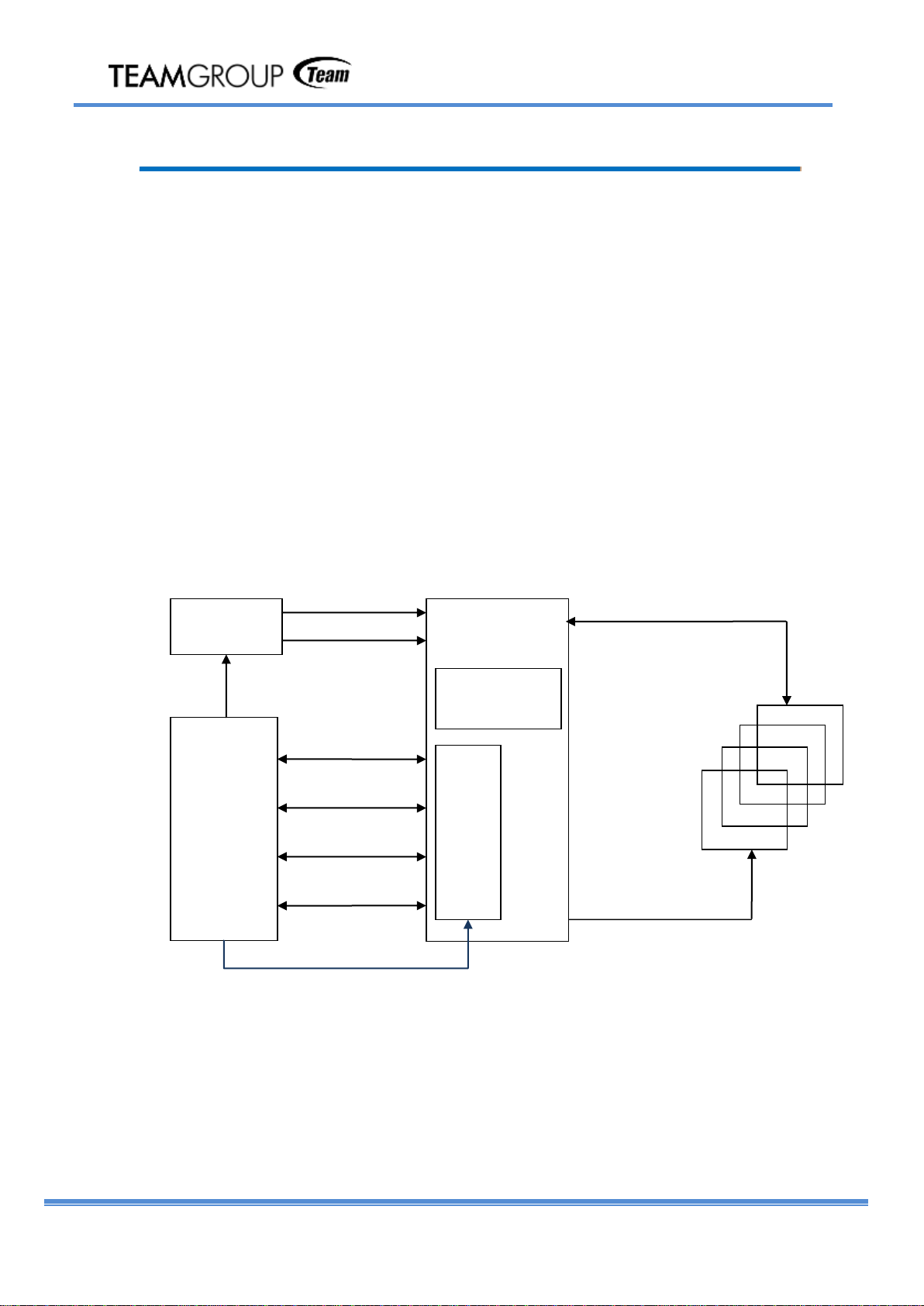
Flash
Controller
Data
Buffer
Data
Flash
DC-DC
Flash memory
SATA
Interface
VCC
Vcore
A+
A-
B+
B-
Control signal
VCC
SATA
PHY
DEVSLP
Team Industrial SATAIII M.2 2260 SSD
1.
INTRODUCTION
1.1 General Description
Team’s M6Q56 M.2 2260 SATA Drive delivers all the advantages of Flash Disk technology
with the Serial ATA I/II/III interface and is fully compliant with the standard Next Generation
Form Factor (NGFF) called M.2 Card Format, which is generated by Intel. The M.2 2260
SATA Drive is designed to operate at a maximum operating frequency of 200MHz with
30MHz external crystal. Its capacity could provide a wide range up to 512GB. Moreover, it
can reach up to 550MB/s read as well as 460MB/s write high performance based on Toshiba
NAND flash (with 32MB SDR enabled and measured by CrystalDiskMark v5.0). The power
consumption of the M.2 2260 is much lower than traditional Hard Drives, making it the best
embedded solution for new platforms.
1.2 Block Diagram

M6Q56 Series
Team Industrial SATAIII M.2 2260 SSD
2
Ver.A01
Capacity:
MLC: From 32GB up to 512GB(Support 48-bit addressing mode)
Electrical/Physical Interface:
SATA Interface
Compliant with SATA Revision 3.2
Compatible with SATA 1.5Gbps, 3Gbps and 6Gbps interface
Support power management
Support expanded register for SATA protocol 48 bits addressing mode
Embedded BIST function for SATA PHY for low cost mass production
Built-in 2-channel NAND flash interface controller
Compliant with Toggle 1.0 and Toggle 2.0 NAND Flash interface
Compliant with ONFI 4.0 interface:
SDR up to mode 5
NV-DDR up to mode 5
NV-DDR2 up to mode 7
NV-DDR3 up to mode 8
Supported NAND Flash:
Support up to 16 Flash Chip Enables (CE) within single design
Toshiba 15nm/3D-NAND MLC and TLC
Support all types of SLC/MLC/TLC/3D-NAND, 8KB/page and 16K/page NAND flash
Support ONFI 2.3, ONFI 3.0, ONFI 3.2 and ONFI 4.0 interface: 2 channels at
maximum
ECC Scheme
Applies the LDPC (Low Density Parity Check) of ECC algorithm
UART Function
GPIO
Support SMART and TRIM commands
2.
PRODUCT SPECIFICATIONS
M6Q56 Series
Team Industrial SATAIII M.2 2260 SSD
3
Ver.A01
Performance
Capacity
Flash
Structure
Flash Type
Sequential
Read
Write
32GB
32GB x 1
BGA, 15nm
550
160
64GB
32GB x 2
BGA, 15nm
550
310
128GB
64GB x 2
BGA, 15nm
550
460
256GB
64GB x 4
BGA, 15nm
550
460
512GB
128GB x 4
BGA, 15nm
550
460
Note:
1. The performance was estimated based on Toshiba NAND flash.
2. Performance may differ according to flash configuration and platform.
3. The table above is for reference only.
TBW (Terabytes Written)
Capacity
Flash Structure
TBW
32GB
32GB x 1
13
64GB
32GB x 2
30
128GB
64GB x 2
87
256GB
64GB x 4
198
512GB
128GB x4
544
Note:
1. Samples were built using Toshiba NAND flash.
2. TBW may differ according to flash configuration and platform.
3. The endurance of SSD could be estimated based on user behavior, NAND endurance
cycles, and write amplification factor. It is not guaranteed by flash vendor.

M6Q56 Series
Team Industrial SATAIII M.2 2260 SSD
4
Ver.A01
Capacity
MLC: 32GB up to 512GB
SATA Interface
SATA Revision 3.2
SATA 1.5Gbps, 3Gbps, and 6Gbps
interface
Flash Interface
Flash Type: MLC
Performance
Read: up to 550 MB/s
Write: up to 460 MB/s
Power Consumption
Active mode: < 1740mW
Idle mode: < 265mw
TBW (Terabyte Written)
544TBW for 512GB
MTBF
More than 2,000,000 hours
Advanced Flash Management
Static and Dynamic Wear Leveling
Bad Block Management
TRIM
SMART
Over-Provision
Low Power Management
DEVSLP Mode (Optional)
DIPM/HIPM Mode
Temperature Range
Operation(Standard): 0 ~ 70°C
Storage: -40°C ~ 85°C
RoHS compliant
Overview

M6Q56 Series
Team Industrial SATAIII M.2 2260 SSD
5
Ver.A01
Table of Contents
1. Introduction ............................................................................................................... …1
1.1 General Description ......................................................................................... 1
1.2 Block Diagram .................................................................................................. 1
2. Product Specifications ................................................................................................... 2
3. Environmental Specifications ....................................................................................... 6
3.1 Environmental Conditions .............................................................................. 6
3.2
MTBF
................................................................................................................ 8
3.3 Certification & Compliance ............................................................................ 8
4.
ELECTRICAL SPECIFICATIONS
............................................................................ 9
4.1 Supply Voltage .................................................................................................. 9
4.2 Power Consumption ......................................................................................... 9
5.
INTERFACE
................................................................................................................ 10
5.1 Pin Assignment and Descriptions ................................................................. 10
6.
SUPPORTED COMMANDS
6.1
ATA Command List
...................................................................................... 13
....................................................................................... 13
6.2 Identify Device Data ....................................................................................... 15
7. Physical Dimension ..................................................................................................... 20
8. Product Ordering Number ......................................................................................... 21
9. Revision Histories ........................................................................................................ 22
M6Q56 Series
Team Industrial SATAIII M.2 2260 SSD
6
Ver.A01
Temperature
Humidity
Test Time
Operation (Standard Grade)
70°C
0% RH
72 hours
Storage (Standard Grade)
85°C
0% RH
72 hours
Temperature
Humidity
Test Time
Operation (Standard Grade)
0°C
0% RH
72 hours
Storage (Standard Grade)
-40°C
0% RH
72 hours
Temperature
Humidity
Test Time
Operation (Standard Grade)
40°C
90% RH
4 hours
Storage (Standard Grade)
40°C
93% RH
72 hours
Temperature
Test Time
Cycle
Operation
(Standard Grade)
0°C
30min
10 Cycle
70°C
30min
Storage
(Standard Grade)
-40°C
30min
10 Cycle
85°C
30min
3.
ENVIRONMENTAL SPECIFICATIONS
3.1
Environmental Conditions
3.1.1 Temperature and Humidity
Storage Temperature Range:
-40°C ~ 85°C
Operation Temperature Range:
Standard Grade: 0°C ~ 70°C
Humidity:
Standard Grade: RH 90% under 40°C (in operational)
High Temperature Test Condition:
Result: No any abnormality is detected.
Low Temperature Test Condition:
Result: No any abnormality is detected.
High Humidity Test Condition:
Result: No any abnormality is detected.
Temperature Cycle Test:
Result: No any abnormality is detected.
M6Q56 Series
Team Industrial SATAIII M.2 2260 SSD
7
Ver.A01
Acceleration Force
Half Sin Pulse Duration
Non-Operational
1500G
0.5ms
Condition
Vibration
Orientation
Frequency/Displacement
Frequency/Acceleration
Non-Operational
20Hz~80Hz/1.52mm
80Hz~2000Hz/20G
X, Y, Z axis/60
min for each
Height of Drop
Number of Drop
Non-Operational
80cm free fall
6 face of each unit, 2 times
Force
Action
Non-Operational
≥ 20N
Hold 1min/5times
Device
Condition
Temperature
Relative Humidity
+/- 4KV
Result
M.2
512GB
24.0°C
49% (RH)
Device functions are
affected, but EUT will
be back to its normal or
operational state
automatically.
PASS
3.1.2 Shock:
Shock Specification.
Result: No any abnormality is detected when power on.
3.1.3 Vibration:
Vibration Specification
Result: No any abnormality is detected when power on.
3.1.4 Drop:
Drop Specification
Result: No any abnormality is detected when power on.
3.1.5 Bending:
Bending Specification
Result: No any abnormality is detected when power on.
3.1.6 Electrostatic Discharge (ESD):
Contact ESD Specification

M6Q56 Series
Team Industrial SATAIII M.2 2260 SSD
8
Ver.A01
3.2
MTBF, an acronym for Mean Time Between Failures, is a measure of a device’s reliability. It
value represents the average time between a repair and the next failure. The measure is
typically in units of hours. The higher the MTBF value, the higher the reliability of the device.
The predicted result of Team M.2 is more than 2,000,000 hours.
MTBF
3.3 Certification & Com pliance
RoHS
SATA III (SATA Rev. 3.2)
Up to ATA/ATAPI-8 (Including S.M.A.R.T)

M6Q56 Series
Team Industrial SATAIII M.2 2260 SSD
9
Ver.A01
Parameter
Rating
Operating Voltage
3.3V ± 5%
Capacity
Flash
Structure
Flash Type
Read
Write
Partial
Slumber
Idle
DEVSLP
32GB
32GB x 1
BGA, 15nm
1000
1200
12
7
255
4.9
64GB
32GB x 2
BGA, 15nm
1040
1215
12
7
257
4.9
128GB
64GB x 2
BGA, 15nm
1065
1480
12
7
255
4.9
256GB
64GB x 4
BGA, 15nm
1165
1535
12
7
260
4.9
512GB
128GB x 4
BGA, 15nm
1425
1740
14
10
260
4.9
4.
ELECTRICAL SPECIFICATIONS
4.1 Supply Voltage
Supply Voltage of M.2
4.2 Power Consumption
Power Consumption of M.2
Unit: mW
Note:
1. The average value of power consumption is achieved based on 100% conversion
efficiency.
2. The measured power voltage is 3.3V.
3. Samples were built using Toshiba NAND flash and measured under normal temperature.
4. Sequential R/W is measured while testing 4000MB sequential R/W 5 times by
CyrstalDiskMark.
5. Power Consumption may differ according to flash configuration, SDR configuration, and
platform.

M6Q56 Series
Team Industrial SATAIII M.2 2260 SSD
10
Ver.A01
Pin
Segment
Pin Definition
1
CONFIG_3=GND
Ground
2
3.3V
Supply pin
3
GND
Ground
4
3.3V
Supply pin
5
N/C
No Connect
6
N/C
No Connect
7
N/C
No Connect
8
N/C
No Connect
9
N/C or GND
No Connect or Ground
(N/C for Socket 2, and GND for Socket 3)
10
DAS/DSS#
(O)(OD)
Status indicators via LED devices that will be provided by the
system Active Low. A pulled-up LED with series current
limiting resistor should allow for 9mA when On.
11
N/C
No Connect
12
Module Key
13
Module Key
14
Module Key
15
Module Key
16
Module Key
17
Module Key
18
Module Key
19
Module Key
20
N/C
No Connect
21
CONFIG_0=GND
Ground
22
N/C
No Connect
23
N/C
No Connect
24
N/C
No Connect
25
N/C
No Connect
26
N/C
No Connect
27
GND
Ground
28
N/C
No Connect
5.
INTERFACE
5.1 Pin Assignment and Descriptions
Pin Assignment and Description of M.2

M6Q56 Series
Team Industrial SATAIII M.2 2260 SSD
11
Ver.A01
29
N/C
No Connect
30
N/C
No Connect
31
N/C
No Connect
32
N/C
No Connect
33
GND
Ground
34
N/C
No Connect
35
N/C
No Connect
36
N/C
No Connect
37
N/C
No Connect
38
DEVSLP(I)
(0/3.3V)
Device Sleep, Input.
When driven high the host is informing the SSD to enter a low power
state
39
GND
Ground
40
N/C
No Connect
41
SATA-B+
SATA differential signals in the SATA specification
42
N/C
No Connect
43
SATA-B-
SATA differential signals in the SATA specification
44
N/C
No Connect
45
GND
Ground
46
N/C
No Connect
47
SATA-A-
SATA differential signals in the SATA specification
48
N/C
No Connect
49
SATA-A+
SATA differential signals in the SATA specification
50
N/C
No Connect
51
GND
Ground
52
N/C
No Connect
53
N/C
No Connect
54
N/C
No Connect
55
N/C
No Connect
56
Reserved for MFG
Data
Manufacturing Data line. Used for SSD manufacturing only.
Not used in normal operation. Pins should be left N/C in
platform Socket
57
GND
Ground
58
Reserved for MFG
Clock
Manufacturing Clock line. Used for SSD manufacturing only.
Not used in normal operation. Pins should be left N/C in

M6Q56 Series
Team Industrial SATAIII M.2 2260 SSD
12
Ver.A01
platform Socket
59
Module Key
60
Module Key
61
Module Key
62
Module Key
63
Module Key
64
Module Key
65
Module Key
66
Module Key
67
N/C
No Connect
68
SUSCLK(I)(0/3.3V)
32 KHz clock supply input that is provided by PCH to reduce
power and cost for the module.
69
CONFIG_1=GND
Defines module type
70
3.3V
Supply pin
71
GND
Ground
72
3.3V
Supply pin
73
GND
Ground
74
3.3V
Supply pin
75
CONFIG_2=GND
Ground

M6Q56 Series
Team Industrial SATAIII M.2 2260 SSD
13
Ver.A01
Op-Code
Command Description
Op-Code
Command Description
00h
NOP
60h
Read FPDMA Queued
06h
Data Set Management
61h
Write FPDMA Queued
10h
Recalibrate
70h
Seek
20h
Read Sectors
90h
Execute Device Diagnostic
21h
Read Sectors without Retry
91h
Initialize Device Parameters
24h
Read Sectors EXT
92h
Download Microcode
25h
Read DMA EXT
93h
Download Microcode DMA
27h
Read Native Max Address EXT
B0h
SMART
29h
Read Multiple EXT
B0h
D0h
SMART READ DATA
2Fh
Read Log EXT
B0h
D1h
SMART READ DATA
ATTRIBUTE THRESHOLD
30h
Write Sectors
B0h
D2h
SMART ENABLE/DISABLE
ATTRIBUTE AUTOSAVE
31h
Write Sectors without Retry
B0h
D3h
SMART SAVE ATTRIBUTE
VALUES
34h
Write Sectors EXT
B0h
D4h
SMART EXECUTE OFF-LINE
IMMEDIATE
35h
Write DMA EXT
B0h
D5h
SMART READ LOG
37h
Set Native Max Address EXT
B0h
D6h
SMART WRITE LOG
39h
Write Multiple EXT
B0h
D8h
SMART ENABLE
OPERATIONS
3Dh
Write DMA FUA EXT
B0h
D9h
SMART DISABLE
OPERATIONS
3Fh
Write Long EXT
B0h
DAh
SMART RETURN STATUS
40h
Read Verify Sectors
B0h
DBh
SMART ENABLE/DISABLE
AUTOMATIC OFF-LINE
41h
Read Verify Sectors without
Retry
B1h
DEVICE CONFIGURATION
OVERLAY
42h
Read Verify Sectors EXT
B1h
C0h
DEVICE CONFIGURATION
RESTORE
45h
Write Uncorrectable EXT
B1h
C1h
DEVICE CONFIGURATION
FREEZE LOCK
47h
Read Log DMA EXT
B1h
C2h
DEVICE CONFIGURATION
6.
SUPPORTED COMMANDS
6.1
ATA Command List

M6Q56 Series
Team Industrial SATAIII M.2 2260 SSD
14
Ver.A01
IDENTIFY
57h
Write Log DMA EXT
B1h
C3h
DEVICE CONFIGURATION
SET
B1h
C4h
DEVICE CONFIGURATION
IDENTIFY DMA
ECh
Identify Device
B1h
C5h
DEVICE CONFIGURATION
SET DMA
EFh
Set Features
C4h
Read Multiple
EFh
02h
Enable 8-bit PIO transfer mode
C5h
Write Multiple
EFh
03h
Set transfer mode based on value
in Count field
C6h
Set Multiple Mode
EFh
05h
Enable advanced power
management
C8h
Read DMA
EFh
10h
Enable use of Serial ATA feature
C9h
Read DMA without Retry
EFh
10h
02h
Enable DMA Setup FIS
Auto-Activate optimization
CAh
Write DMA
EFh
10h
03h
Enable Device-initiated interface
power state (DIPM) transitions
CBh
Write DMA without Retry
EFh
10h
06h
Enable Software Settings
Preservation (SSP)
CEh
Write Multiple FUA EXT
EFh
10h
07h
Enable Device Automatic Partial
to Slumber transitions
E0h
Standby Immediate
EFh
10h
09h
Enable Device Sleep
E1h
Idle Immediate
EFh
55h
Disable read look-ahead feature
E2h
Standby
EFh
66h
Disable reverting to power-on
defaults
E3h
Idle
EFh
82h
Disable write cache
E4h
Read Buffer
EFh
85h
Disable advanced power
management
E5h
Check Power Mode
EFh
90h
Disable use of Serial ATA feature
set
E6h
Sleep
EFh
90h
02h
Disable DMA Setup FIS
Auto-Activate optimization
E7h
Flush Cache
EFh
90h
03h
Disable Device-initiated interface
power state (DIPM) transitions
E8h
Write Buffer
EFh
90h
06h
Disable Software Settings
Preservation (SSP)
E9h
Read Buffer DMA
EFh
90h
07h
Disable Device Automatic Partial

M6Q56 Series
Team Industrial SATAIII M.2 2260 SSD
15
Ver.A01
to Slumber transitions
EAh
Flush Cache EXT
EFh
90h
09h
Disable Device Sleep
EBh
Write Buffer DMA
EFh
AAh
Enable read look-ahead feature
EFh
CCh
Enable reverting to power-on
defaults
F4h
Security Erase Unit
F1h
Security Set Password
F5h
Security Freeze Lock
F2h
Security Unlock
F6h
Security Disable Password
F3h
Security Erase Prepare
F8h
Read Native Max Address
Word
F:Fixed
V:Variable
X:Both
Default Value
Description
0
F
0040h
General configuration bit-significant
information
1
X
*1
Obsolete – Number of logical cylinders
2
V
C837
Specific configuration
3
X
0010h
Obsolete – Number of logical heads
(16)
4-5
X
00000000h
Retired
6
X
003Fh
Obsolete – Number of logical sectors
per logical track (63)
7-8
V
00000000h
Reserved for assignment by the
Compact Flash Association
9
X
0000h
Retired
10-19
F
Varies
Serial number (20 ASCII characters)
20-21
X
0000h
Retired
22
X
0000h
Obsolete
23-26
F
Varies
Firmware revision (8 ASCII characters)
27-46
F
Varies
Model number (xxxxxxxx)
47
F
8010h
7:0- Maximum number of sectors
transferred per interrupt on MULTIPLE
commands
48
F
4000h
Trusted Computing feature set
options(not support)
6.2 Identify Device Data
The following table details the sector data returned by the IDENTIFY DEVICE command.

M6Q56 Series
Team Industrial SATAIII M.2 2260 SSD
16
Ver.A01
49
F
2F00h
Capabilities
50
F
4000h
Capabilities
51-52
X
00000000h
Obsolete
53
F
0007h
Words 88 and 70:64 valid
54
X
*1
Obsolete – Number of logical cylinders
55
X
0010h
Obsolete – Number of logical heads
(16)
56
X
003Fh
Obsolete – Number of logical sectors
per track (63)
57-58
X
*2
Obsolete – Current capacity in sectors
59
F
0110h
Number of sectors transferred per
interrupt on MULTIPLE commands
60-61
F
*3
Maximum number of sector ( 28bit
LBA mode)
62
X
0000h
Obsolete
63
F
0407h
Multi-word DMA modes
supported/selected
64
F
0003h
PIO modes supported
65
F
0078h
Minimum Multiword DMA transfer
cycle time per word
66
F
0078h
Manufacturer’s recommended
Multiword DMA transfer cycle time
67
F
0078h
Minimum PIO transfer cycle time
without flow
68
F
0078h
Minimum PIO transfer cycle time with
IORDY flow control
69
F
0100h
Additional Supported (support
download microcode
70
F
0000h
Reserved
71-74
F
0000000000000000h
Reserved for the IDENTIFY PACKET
DEVICE command
75
F
001Fh
Queue depth
76
F
670eh
Serial SATA capabilities
77
F
0084h
Serial ATA Additional Capabilities
78
F
014Ch
Serial ATA features supported
79
V
0040h
Serial ATA features enabled
80
F
07F8h
Major Version Number

M6Q56 Series
Team Industrial SATAIII M.2 2260 SSD
17
Ver.A01
81
F
0000h
Minor Version Number
82
F
346bh
Command set supported
83
F
7d09h
Command set supported
84
F
6063h
Command set/feature supported
extension
85
V
3469h
Command set/feature enabled
86
V
bc01h
Command set/feature enabled
87
V
6063h
Command set/feature default
88
V
003Fh
Ultra DMA Modes
89
F
0001h
Time required for security erase unit
completion
90
F
001Eh
Time required for Enhanced security
erase
91
V
0000h
Current advanced power management
value
92
V
FFFEh
Master Password Revision Code
93
F
0000h
Hardware reset result. The contents of
the bits (12:0) of this word can be
changed only during the execution of
hardware reset.
94
V
0000h
Vendor’s recommended and actual
acoustic management value
95
F
0000h
Stream Minimum Request Size
96
V
0000h
Streaming Transfer Time – DMA
97
V
0000h
Streaming Access Latency – DMA and
PIO
98-99
F
0000h
Streaming Performance Granularity
100-103
V
*4
Maximum user LBA for 48 bit Address
feature set
104
V
0000h
Streaming Transfer Time – PIO
105
F
0008h
Maximum number of 512-byte blocks
per DATA SET MANAGEMENT
command
106
F
4000h
Physical sector size/Logical sector size
107
F
0000h
Inter-seek delay for ISO-7779 acoustic
testing in microseconds
108-111
F
0000000000000000h
Unique ID

M6Q56 Series
Team Industrial SATAIII M.2 2260 SSD
18
Ver.A01
112-115
F
0000000000000000h
Reserved
116
V
0000h
Reserved
117-118
F
00000000h
Words per logical Sector
119
F
4014h
Supported settings
120
F
4014h
Command set/Feature
Enabled/Supported
121-126
F
0h
Reserved
127
F
0h
Removable Media Status Notification
feature set support
128
V
0021h
Security status
129-140
X
0h
Vendor specific
141
X
0001h
Vendor specific
142-159
X
0h
Vendor specific
160
F
0h
Compact Flash Association (CFA)
power mode 1
161-167
X
0h
Reserved for assignment by the CFA
168
F
3h 2.5 inch
4h 1.8 inch
5h Less than 1.8inch
Device Nominal Form Factor
169
F
0001h
DATA SET MANAGEMENT
command is
170-173
F
0h
Additional Product Identifier
174-175
0h
Reserve
176-205
V
0h
Current media serial number
206
F
0h
SCT Command Transport
207-208
F
0h
Reserved
209
F
4000h
Alignment of logical blocks within a
physical block
210-211
V
0000h
Write-Read-Verify Sector Count Mode
3 (not support)
212-213
F
0000h
Write-Read-Verify Sector Count Mode
2 (not support)
214-216
0000h
NV Cache relate (not support)
217
F
0001h
Non-rotating media device
218
F
0h
Reserved
219
F
0h
NV Cache relate (not support)
220
V
0h
Write read verify feature set current

M6Q56 Series
Team Industrial SATAIII M.2 2260 SSD
19
Ver.A01
mode
221
0h
Reserved
222
F
107Fh
Transport major version number
223
F
0h
Transport minor version number
224-229
0h
reserved
230-233
0h
Extend number of user addressable
sectors
234
0001h
Minimum number of 512-byte data
blocks per DOWNLOAD
MICROCODE command for mode
235
0080h
Maximum number of 512-byte data
blocks per DOWNLOAD
MICROCODE command for mode
236-254
F
0h
Reserved
255
X
XXA5h XX is variable
Integrity word (Checksum and
Signature)
Capacity
(GB)
*1
(Word 1/Word 54)
*2
(Word 57 - 58)
*3
(Word 60 - 61)
*4
(Word 100 - 103)
32
3FFFh
FBFC10h
3BA2EB0h
3BA2EB0h
64
3FFFh
FBFC10h
7740AB0h
7740AB0h
128
3FFFh
FBFC10h
EE7C2B0H
EE7C2B0H
256
3FFFh
FBFC10h
FFFFFFFh
1DCF32B0h
512
3FFFh
FBFC10h
FFFFFFFh
3B9E12B0h
List of Device Identification for Each Capacity

M6Q56 Series
Team Industrial SATAIII M.2 2260 SSD
20
Ver.A01
7.
PHYSICAL DIMENSION
Dimension: 60mm(L) x 22mm(W) x 3.75mm(H)

M6Q56 Series
Team Industrial SATAIII M.2 2260 SSD
21
Ver.A01
TIM6Q56
XXXX X X
104
Team Industrial
SATAIII M.2
2260 SSD
032G:32GB
064G:64GB
128G:128GB
256G:256GB
512G:512GB
M : MLC
C : 0°C ~70°C
Bulk Packing
Capacity
Product Ordering Number
32GB
TIM6Q56032GMC104
64GB
TIM6Q56064GMC104
128GB
TIM6Q56128GMC104
256GB
TIM6Q56256GMC104
512GB
TIM6Q56512GMC104
8. PRODUCT ORDERING NUMBER
The ordering number rule is as below:
The products list is as below:

M6Q56 Series
Team Industrial SATAIII M.2 2260 SSD
22
Ver.A01
Version
Revision Description
Date
Issued By
Authorized By
A01
Initial Release
2017/12/14
Jerry.Chien
Tommy.Hua
9. REVISION HISTORIES
 Loading...