


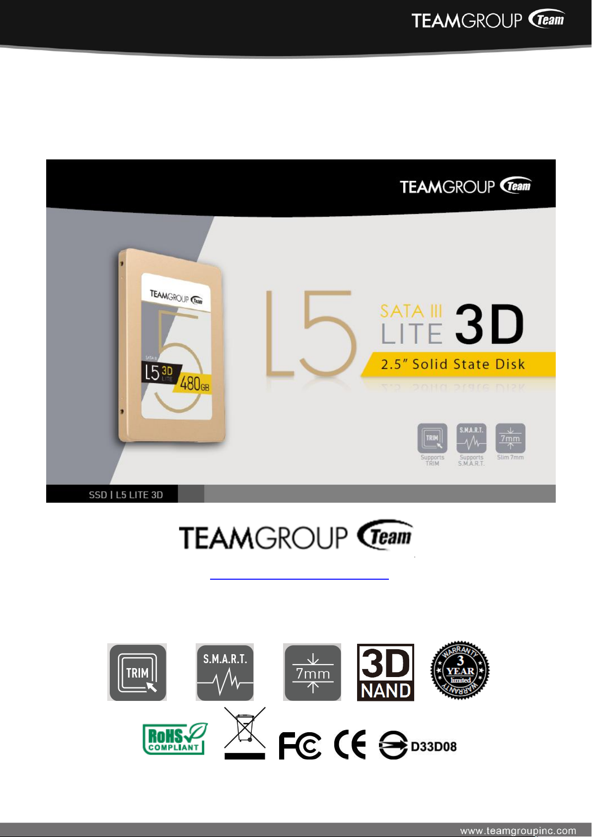
Team Group Solid State drive
L5 LITE 3D SSD SATA III (2.5” Inch)
http://www.teamgroupinc.com
All rights are strictly reserved. Any portion of this paper shall not be reproduced, copied,
or translated to any other forms without permission from TEAMGROUP.

TEAM GROUP INC.
Table of Contents
1. General Description................................................................................................... 1
2. Mechanical Specification........................................................................................... 3
3. Product Specifications............................................................................................... 4
4. Electrical Interface Specification.............................................................................. 6
5. Command Descriptions............................................................................................. 7
6. Identify Device Data.................................................................................................. 9
7. Ordering Number…….............................................................................................. 12

Version
Revision Description
Date
Remark
A.0
Initial Release
15-SEP-2017
Steve Lin
TEAM GROUP INC.
Revision Histories
Documentation Revise History:
TEAM GROUP INC.
1. General Description
The latest generation of 3D NAND flash memory has overcome the technical barrier of 2D NAND,
and has enhanced the overall capacity, performance and reliability. Unlike the 2D planar flash memory,
3D NAND increases storage capacity by stacking up cells in vertical direction. It not only provides a
better performance and endurance, but also breaks through the technical limitation of planar chips.
The L5 LITE 3D solid state drive is 4 times faster than the traditional hard drive. Its excellent
performance and read/write speed not only allow fast boot/shutdown time, but also speed up the response
time of all applications, so consumers can enjoy the high speed performance immediately after the
upgrade. The lightweight and zero hassle advantage make it the best product to replace traditional hard
drive.
The L5 LITE 3D solid state drive has an industry-standard 2.5-inch. With only 7mm in height, it is
best suited for Ultrabooks on the market. Whether it is for laptop or desktop, the upgrade can be done
quickly. It is using SATA III 6Gbps specification and capacities available in 120GB, 240GB, 480GB, etc.
With read speed up to 470 MB/s, it not only improves the computer performance, but it is also the best
bargain available.
The L5 LITE 3D solid state drive is using 3D NAND flash memory chip, which is durable,
shockproof, drop resistant and offers a total protection for the data. Even if you accidently drop your
computer or it landed on a hard surface, it can still prevent damages and data corruption from accidents.
The L5 LITE 3D solid state drive supports Windows TRIM optimization command which is able to
release free blocks, allowing operating system to use them later immediately when writing data. The
optimized access control technology of NCQ can speed up the transfer and write performance of the SSD,
and effectively reduces performance degradation and wear and tear of the drive. This can prolong the
service life of the SSD perfectly.
L5 LITE 3D solid state drive’s built-in smart algorithm management mechanism has functions such
as garbage collection which is able to ensure operation efficiency. The powerful Wear-Leveling
technology and ECC (Error Correction Code) function enhance the reliability of data transfer.
1

Item
Specification
Model
L5 LITE 3D
Interface
SATA Rev. 3.0 (6Gb/s) – with backwards compatibility to SATA Rev.
2.0
Capacity
120 / 240 / 480GB*
Color
Gold
Voltage
DC 5V
Operation Temperature
0°C ~ 70°C
Performance
ATTO / Crystal Disk Mark:
120GB Read: 470MB/s ; Write: 300MB/s
240GB Read: 470MB/s ; Write: 400MB/s
480GB Read: 470MB/s ; Write: 420MB/s
IOPS:
120GB 4K Random Read/Write: 30K/40K IOPS max
240GB 4K Random Read/Write: 65K/70K IOPS max
480GB 4K Random Read/Write: 70K/70K IOPS max**
Weight
65g
Dimensions
100(L) x 69.85(W) x 7(H) mm
Humidity
0°C to 55°C / 5% ~ 95% RH, non-condensing
Vibration
20G (non-operating)
Shock
1500G
MTBF
1,000,000 hours
System Requirements
Windows 10 / 8 / 7 / Vista, MAC OS 10.4 or later, Linux
2.6.33 or later
Warranty
3-year limited warranty
TEAM GROUP INC.
Main Feature
3D NAND – excellent choice for upgrade
Read/write speed is 4 times faster than traditional hard drive – breathe new life into old system
Smooth read/write speed – up to 470 MB/s of read speed is able to enhance the speed and
performance of the overall system
Ultra lightweight and slim - 2.5-inch hard drive with just 7.0 mm thickness, it can be installed on
laptop or any other system
Support S.M.A.R.T. technology - monitoring hard drive status efficiently
Support TRIM - bring out its best performance on the compatible operating system
Three years product warranty with free technical support service
Notes: *1GB=1,000,000,000 Bytes. In OS system, it would be displayed as 1,000,000,000 Bytes / 1024 / 1024 / 1024 = 0.93GB
**Transmission speed will vary according to different hardware / software conditions, therefore the data can only used for basic
reference.
※We reserve the right to modify product specifications without prior notice.
2

Height (mm)
Width (mm)
Length (mm)
Weight (gram)
7.00 (+/- 0.15)
69.85 (+/- 0.15)
100.00 (+/- 0.15)
65g (Max)
TEAM GROUP INC.
SSD Functional Block Diagram
2. Mechanical Specification
2.1 2.5 inch SSD physical dimensions and Weight
inch2.5 plastic shell Physical dimension (top)
3

SATA 6Gb/s host interface
Parameter
Unit
120GB
240GB
480GB
Sequential Read
MB/S
470(Max)*
470(Max)*
470(Max)*
Sequential Write
MB/S
300(Max)*
400(Max)*
420(Max)*
Random Read(4K) QD=32
IOPS
30K(Max)*
65K(Max)*
70K(Max)*
Random Write(4K) QD=32
IOPS
40K(Max)*
70K(Max)*
70K(Max)*
Unformatted Capacity
120GB
240GB
480GB
Total Number of User-Addressable
Sectors in LBA Mode
234375000
468750000
937500000
Bytes per Sector
512 Bytes
Item
Requirements
Allowable voltage
5.0V +/- 5%
Allowable noise / ripple
100mV p-p or less
Input Voltage 5.0 +/- 5% (mA)
Parameter
120GB
240GB
480GB
Idle
149.4
148.8
140.6
Sequential Read
431.4
430.9
326.9
Sequential Write
382.5
405.5
410.5
TEAM GROUP INC.
3. Product Specification
3.1 System Interface and Configuration
Burst read/write rate is 600 MB/sec (6.0 Gb/sec).
3.2 System Performance
Note: Actual performance may vary depending on use conditions and environment.
3.3 Drive Capacity
Note:
* 1 Megabyte (MB) = 1 Million byte;1 Gigabyte (GB) = 1 Billion bytes.
**Actual usable capacity may be less (due to formatting, partitioning, operating system, and applications or otherwise)
3.4 Supply Voltage
3.5 System Power Consumption
3.6 System Reliability
MTBF: 1,000,000 Hours
*MTBF is Mean Time between Failures. As same word, annual failure ratio is 0.4%.
4

Features
Operating
Non-Operating
Temperature
0°C to 70°C
-40°C to 85°C
Humidity
5% to 95%, non-condensing
Vibration
7~800Hz, 3.08Grms, 30min / axis (X,Y,Z)
Shock
1500G, duration 0.5ms, Half Sine Wave
TEAM GROUP INC.
3.7 Environmental Specifications
Note:
*Temperature specification is following JEDEC standard; Expressed temperature must be measured right on the
**Humidity is measured in non-condensing.
***Test condition for shock: 0.5ms duration with half sine wave.
****Test condition for vibration: 10Hz to 2,000Hz, 15mins/axis on 3axis
case.
5

Plug connector pin definition
Signal
S1
GND
2
nd
mate
S2
A+
Differential signal A from phy
S3
A-
S4
GND
2
nd
mate
S5
B-
Differential signal B from phy
S6
B+
S7
GND
2
nd
mate
Key and spacing separate signal and power segments
Power
P1
V33
3.3V power (Unused)
P2
V33
3.3V power (Unused)
P3
V33
3.3V power, pre-charge, 2
nd
mate (Unused)
P4
GND
1
st
mate
P5
GND
2
nd
mate
P6
GND
2
nd
mate
P7
V5
5V power, pre-charge, 2
nd
mate
P8
V5
5V power
P9
V5
5V power
P10
GND
2
nd
mate
P11
DAS / DSS
Device Activity Signal / Disable Staggered Spinup
P12
GND
1
st
mate
P13
V12
12V power, pre-charge, mate (Unused)
P14
V12
12V power (Unused)
P15
V12
12V power (Unused)
TEAM GROUP INC.
4. Electrical Interface Specification
4.1 2.5 inch Connector Pin Assignments
6

Command
Code
Protocol
General Feature Set
Execute Device Diagnostic
90h
Execute device diagnostic
Flush Cache
E7h
Non-data
Identify Device
ECh
PIO
Initialize Drive Parameters
91h
Non- data
Read DMA
C8h
DMA
Read Log Ext
2Fh
PIO
Read Multiple
C4h
PIO
Read Sector(s)
20h
PIO
Read Verify Sector(s)
40h or 41h
Non- data
Set Feature
EFh
Non- data
Set Multiple Mode
C6h
Non- data
Write DMA
CAh
DMA
Write Multiple
C5h
PIO data-out
Write Sector(s)
30h
PIO data-out
NOP
00h
Non- data
Read Buffer
E4h
PIO
Write Buffer
E8h
PIO data-out
Power Management Feature Set
Check Power Mode
E5h or 98h
Non- data
Idle
E3h or 97h
Non- data
Idle Immediate
E1h or 95h
Non- data
Sleep
E6h or 99h
Non- data t
Standby
E2h or 96h
Non- data
Standby Immediate
E0h or 94h
Non- data
SMART Feature Set
SMART Read Data
B0h
PIO data-in
SMART Read Threshold
B0h
PIO data-in
Host Protected Area Feature Set
Read Native Max Address
F8h
Non-data
48-bit Address Feature Set
Flush Cache Ext
EAh
Non-data
Read Sector(s) Ext
24h
PIO data-in
Read DMA Ext
25h
DMA
Read Multiple Ext
29h
PIO data-in
Read Native Max Address Ext
27h
Non-data
Read Verify Sector(s) Ext
42h
Non-data
Write DMA Ext
35h
DMA
TEAM GROUP INC.
5. Command Descriptions
5.1 Supported ATA Commands
7

Write Multiple Ext
39h
PIO data-out
Write Sector(s) Ext
34h
PIO data-out
NCQ Feature Set
Read FPDMA Queued
60h
DMA Queued
Write FPDMA Queued
61h
DMA Queued
Others
Data Set Management
06h
DMA
Seek
70h
Non-data
Attribute ID (hex)
Attribute Name
01
Read Error Rate
*02
Throughput Performance
*03
Spin Up Time
*05
Reallocated Sectors Count
*07
Seek Error Rate
*08
Seek Time Performance
09
Power-On Hours
*0A
Spin Retry Count
0C
Power Cycle Count
A8
SATA PHY Error Count
AA
“Bad Block Count (Early / Later)”
AD
Erase count (Average, Max Erase Count)
*AF
Bad Cluster Table Count
BB
Uncorrectable Errors
C0
Unsafe Shutdown Count
C2
Temperature
*C4
Later Bad Block Count
*C5
Current Pending Sector Count
C7
CRC Error Count
DA
CRC Error Count
E7
SSD Life Left
E9
Lifetime Writes to Flash
*F0
Write Head
F1
Host Writes (Sector Unit)
F2
Host Reads (Sector Unit)
F4
Average Erase Count
F5
Max Erase Count
F6
Total Erase Count
* These fields are included for compatibilty with legacy systems and return fixed values.
TEAM GROUP INC.
5.2 SMART Attributes
8

Word
F / V
Default
Value
Description
0 F 0040h
General configuration
1
X
XXXXh
Default number of cylinders
2 V 0000h
Reserved
3 X 00XXh
Default number of heads
4 X 0000h
Obsolete
5 X 0240h
Obsolete
6
F
XXXXh
Default number of sectors per track
7 - 8
V
XXXXh
Number of sectors per card
(Word 7 = MSW, Word 8 = LSW)
9 X 0000h
Obsolete
10 – 19
F
XXXXh
Serial number in ASCII (Right justified)
20 X 0002h
Obsolete
21 X 0002h
Obsolete
22 X 0000h
Obsolete
23 – 26
F
XXXXh
Firmware revision in ASCII
Big Endian Byte Order in Word
27 – 46
F
XXXXh
Model number in ASCII (Left justified)
Big Endian Byte Order in Word
47 F 8001h
Maximum number of sectors on Read/Write Multiple command
48 F 0000h
Reserved
49 F 0F00h
Capabilities
50 F 4000h
Capabilities
51 F 0200h
PIO data transfer cycle timing mode
52 X 0000h
Obsolete
53 F 0007h
Field validity
54
X
XXXXh
Current numbers of cylinders
55
X
XXXXh
Current numbers of heads
56
X
XXXXh
Current sectors per track
57 - 58
X
XXXXh
Current capacity in sectors (LBAs)
(Word 57 = LSW , Word 58 = MSW)
59 F 0101h
Multiple sector setting
60 – 61
F
XXXXh
Total number of user addressable logical sectors for 28-bit
TEAM GROUP INC.
6. Identify Device Data
The Identify Device command enables the host to receive parameter information from the controller. This
command has the same protocol as the Read Sector(s) command. The parameter words in the buffer have
the arrangement and meanings defined in the following table.
ID Table Information
9

commands (DWord)
62 X 0000h
Reserved
63 F 0007h
Multiword DMA transfer
Supports MDMA mode 0, 1 and 2
64 F 0003h
Advanced PIO modes supported
65 F 0078h
Minimum Multiword DMA transfer cycle time per word
66 F 0078h
Recommended Multiword DMA transfer cycle time
67 F 0078h
Minimum PIO transfer cycle time without flow control
68 F 0078h
Minimum PIO transfer cycle time with lORDY flow control
69 F 4000h
Additional supported
70 – 74
F
0000h
Reserved
75 F 001Fh
Queue depth
76
F
E70Eh
Serial ATA capabilities
• Supports Serial ATA Gen3
• Supports Serial ATA Gen2
• Supports Serial ATA Gen1
• Supports Phy event counters log
• Supports receipt of host initiated power management requests
• Supports Native Command Queuing
77 F 0080h
Serial ATA additional capability
• DevSleep_to_ReducedPwerState
78 F 0148h
Serial ATA features supported
• Supports Device Sleep
• Supports software settings preservation
• Device supports initiating power management
79 V 0040h
Reserved
80 F 03F0h
Major version number (ACS-2)
81 F 0000h
Minor version number
82 F 742Bh
Command sets supported 0
83 F 7500h
Command sets supported 1
84 F 4023h
Command sets supported 2
85 - 87
V
XXXXh
Command set/feature enabled
88 V 007Fh
Ultra DMA mode supported and selected
89 F 0003h
Time required for a Normal Erase mode Security Erase Unit
command
90 F 0001h
Time required for an Enhanced Erase mode Security Erase Unit
command
91 V 0000h
Current advanced power management value
92
V
FFFEh
Master password identifier
93 - 99
V
0000h
Reserved
100 –103
V
XXXXh
Maximum user LBA for 48-bit address feature set
TEAM GROUP INC.
10

104
V
0000h
Reserved
105
F
0100h
Maximum number of 512-byte blocks per Data Set Management
command
106 -127
V
0000h
Reserved
128
V
0001h
Security status
129 –159
X
XXXXh
Vendor specific
160
F
0000h
Power requirement description
161
X
0000h
Reserved
162
F
0000h
Key management schemes supported
163
F
0000h
CF Advanced True lDE Timing mode capability and setting
164 -168
V
0000h
Reserved
169
F
0001h
Data Set Management supported
170 –216
V
XXXXh
Reserved
217
F
0001h
Non-rotating media (SSD)
218 -221
X
0000h
Reserved
222
F
107Fh
Transport major revision (SATA Rev 3.1)
223 –254
X
0000h
Reserved
255
X
XXXXh
Integrity word
TEAM GROUP INC.
Note:
1. F = content (byte) is fixed and does not change.
2. V = content (byte) is variable and may change depending on the state of the device or the commands
executed by the device.
3. X = content (byte) is vendor specific and may be fixed or variable.
11

T
25 3 TD
XXXX
3
C
Team P/N
Capacity
Description
T253TD120G3C101
120GB
TEAM 2.5" STD SATA3 L5 LITE 3D 7mm 120GB RETAIL
T253TD240G3C101
240GB
TEAM 2.5" STD SATA3 L5 LITE 3D 7mm 240GB RETAIL
T253TD480G3C101
480GB
TEAM 2.5" STD SATA3 L5 LITE 3D 7mm 480GB RETAIL
TEAM
2.5" STD
SATA
7+15PIN
SMI SATA3
L5 LITE 3D
NAND TLC
120G: 120GB
240G: 240GB
480G: 480GB
3D NAND
C: 0°C - 70°C
TEAM GROUP INC.
7. Ordering Information
The ordering number rule is as below:
12
 Loading...