

TDK Semiconductor Corporation 78Q2120-CGT, 78Q2120-64CGT, 78Q2120-64CG Datasheet
78Q2120
10/100BASE-TX
Ethernet Transceiver
April 2000
DESCRIPTION
The 78Q2120 is a 10BASE-T/100BASE-TX Fast
Ethernet transceiver. It includes integrated MII,
ENDECs, scrambler/descrambler, dual-speed clock
recovery, and full-featured auto-negotiation
functions. The transmitter includes an on-chip pulseshaper and a low-power line driver. The receiver has
an adaptive equalizer and a baseline restoration
circuit required for accurate clock and data recovery.
The transceiver interfaces to Category-5 unshielded
twisted pair (Cat -5 UTP) cabling, and is connected to
the line media via 1:1 isolation transformers. No
external filter is required. Interface to the MAC is
accomplished through an IEEE-802.3 compliant
media independent interface (MII). The product is
fabricated in a BiCMOS process for high
performance and low power operation, and can
operate from a single 3.3 V or 5 V supply.
FEATURES
• 10BASE-T/100BASE-TX IEEE-802.3 compliant TX
and RX functions requiring a dual 1:1 isolation
transformer interface to the line
• Integrated MII, 10BASE-T/100BASE-TX ENDEC,
100BASE-TX scrambler/descrambler, and fullfeatured auto-negotiation function
• Full duplex operation capable
• PCS Bypass supports 5-bit symbol interface
• Dual speed clock recovery
• Automatic polarity correction during auto-
negotiation and 10BASE-T signal reception
• Power-saving and power-down modes including
transmitter disable
• BiCMOS technology, operates with a single 3.3V or
5V supply
• LED indicators: LINK,TX,RX,COL,100,10,FDX
• User programmable Interrupt pin
• General Purpose I/O Interface (80-pin package
only)
• 64 and 80-Lead TQFP (JEDEC LQFP),
64-Pin QFP packages
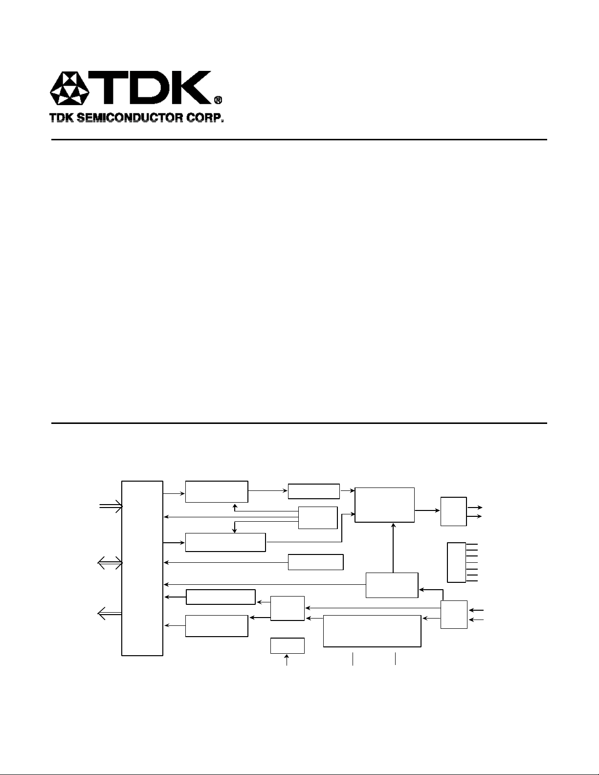
Transmit
MII Serial
Management
& Control
Receive
MII
Registers
&
Interface
Logic
100M
10M
4B/5B Encoder,
Scrambler,
Parallel/Serial
Parallel/Serial,
Manchester Encoder
Manchester Decoder,
Serial/Parallel
Serial/Parallel,
Descrambler,
5B/4B Decoder
BLOCK DIAGRAM
NRZ/NRZI,
MTL3 Encoder
TX Clock
Generator
Carrier Sense,
Collision Detect
Clock
Recovery
Clock
Reference
CKIN
Pulse Shaper
& Filter
Auto
Negotiation
Adaptive EQ,
Baseline Wander Corrector,
MLT3 Decoder,
NRZI/NRZ
Vcc Ground
10M
100M
UTP
Drivers
LEDs
UTP
Receiver
TXOP
TXON
LINK
TX
RX
COL
100BT
10BT
FDX
RXIP
RXIN

78Q2120
10/100BASE-TX
Ethernet Transceiver
FUNCTIONAL DESCRIPTI ON
GENERAL
SUPPLY VOLTAGE
The 78Q2120 can operate from either a single 3.3V
(± 0.3V) or 5.0V (± 0.5V) power supply. The chip
automatically adapts to the supply voltage used. No
pin configuration is required.
POWER MANAGEMENT
The 78Q2120 has three power saving modes:
• Chip Power-Down
• Receive Power Management
• Transmit High Impedance Mode
Chip power-down is activated by setting the PWRDN
bit in the MII register (MR0.11) or pulling high the
PWRDN pin. When the chip is in power- down mode, all
on- chip circuitry is shut off, and the device consumes
minimum power. While in power- down state, the
78Q2120 still responds to management transactions.
Receive power management (RXCC mode) is
activated by setting the RXCC bit in the MII register
(MR16.0). In this mode of operation, the adaptive
equalizer, the clock recovery phase lock loop (PLL),
and all other receive circuitry will be powered down
when no valid signal is present at the UTP receive
line interface. As soon as a valid signal is detected,
all circuits will automatically be powered up to
resume normal operation. During this mode of
operation, RX_CLK will be inactive when there is no
data being received. Note that the RXCC mode is
not supported during 10BASE-T operation.
Transmit high impedance mode is activated by
setting the TXHIM bit in the MII register (MR16.12). In
this mode of operation, the transmit UTP drivers are in
a high impedance state and TXCLK is tri-stated. A
weak internal pull-up is enabled on TXCLK. The
receive circuitry remains fully operational. The default
state of MR16.12 is a logic low for disabling the
transmit high impedance mode. Only a reset condition
will automatically clear MR16.12. The transmitter is
fully functional when MR16.12 is cleared.
ANALOG BIASING
The 78Q2120 uses the reference clock and an external
resistor to generate accurate bias voltages for the chip.
CLOCK SELECTION
The 78Q2120 will default to use the on-chip crystal
oscillator. In this mode a 25MHz crystal is connected
between the XTLP and XTLN pins. The CKIN pin should
be tied low. Alternatively, an externally generated
25MHz clock can be connected to the CKIN pin. The
chip senses activity on the CKIN pin, and will
automatically configure itself to use the external clock.
In this mode of operation, a crystal is not required and
the XTLP and XTLN pins should be connected together.
TRANSMIT CLOCK GENERATION
The transmitter uses an on-chip frequency
synthesizer to generate the transmit clock. In
100BASE-TX operation, the synthesizer multiplies the
reference clock by 5 to obtain the internal 125MHz
serial transmit clock. In 10BASE-T mode, it generates
an internal 20MHz transmit clock by multiplying the
reference 25MHz clock by 4/5. The synthesizer
references either the local 25 MHz crystal oscillator,
or the externally applied clock, depending on the
selected mode of operation.
RECEIVE SIGNAL QUALIFICATION
The integrated signal qualifier has separate squelch
and un-squelch thresholds, and includes a built-in
timer to ensure fast and accurate signal detection and
receive noise rejection. Upon detection of two or
more valid 10BASE-T or 100BASE-TX pulses on the
line receive port, the pass indication, indicating the
presence of valid receive signals or data, will be
asserted. When pass is asserted, the signal detect
threshold is lowered by about 60%, and all adaptive
circuits are released from their quiescent operating
conditions, allowing them to lock onto the incoming
data. In 100BASE-TX operation, pass will be deasserted when no signal is presented for a period of
about 1.2us. In 10BASE-T operation, pass will be deasserted whenever no Manchester data is received.
In either case, the signal detect threshold will return to
the squelched level whenever the pass indication is
de-asserted. The pass signal is used internally to
control the operation of the receive clock recovery.
RECEIVE CLOCK RECOVERY
In 100BASE- TX mode, the 125MHz receive clock is
extracted using a narrow- band PLL. When no receive
signal is present, the PLL is directed to lock onto the
transmit 125 MHz clock. When pass is asserted, the PLL
will use the received NRZI signal as the clock reference.
The recovered clock is used to re- time the data signal and
for conversion of the data to NRZ format.
In 10BASE-T mode, the 10MHz clock is recovered
using a PLL. For fast acquisition, the receive PLL is
locked onto the transmit reference clock during idle
receive periods. When Manchester-coded preambles
are detected, the PLL adjusts its phase and resynchronizes with the incoming Manchester data.
2

100BASE -TX OPERATION
78Q2120
10/100BASE-TX
Ethernet Transceiver
10BASE-T OPERATION
100BASE -TX Transmit
The 78Q2120 contains all of the necessary circuitry
to convert the transmit MII signaling from a MAC to
an IEEE-802.3 compliant data-stream driving Cat-5
UTP cabling. The internal PCS interface maps 4 bit
nibbles from the MII to 5 bit code groups as defined
in table 24-1 of IEEE-802.3. These 5 bit code groups
are then scrambled and converted to a serial stream
before being sent to the MLT-3 pulse shaping
circuitry and line driver. The pulse-shaper uses
current modulation to produce the desired output
waveform. Controlled rise/fall time in MLT-3 signal
is achieved using an accurately controlled C/I filter.
The line driver requires an external 1:1 isolation
transformer to interface with the line media. The
center-tap of the primary side of the transformer
should be connected to Vcc.
100BASE -TX RECEIVE
The 78Q2120 receives a 125MBaud MLT-3 signal
through a 1:1 transformer. The signal then goes through
a combination of adaptive offset adjustment (baseline
wander correction) and adaptive equalization. The
effect of these circuits is to sense the amount of
dispersion and attenuation caused by the cable and
transformer, and restore the received pulses to logic
levels. The amount of gain and equalization applied to
the pulses varies with the detected attenuation and
dispersion and, therefore, with the length of the cable.
The 78Q2120 can recover up to a 10dB of loss in signal
amplitude at 16 MHz. This loss is represented as testchan 5 in AnnexA of the ANSI X3.263:199X
specification and corresponds to approximately 140m of
Cat5 UTP cabling. The equalized MLT-3 data signal is
sliced and the resulting bit-stream is presented to the
clock recovery PLL and to a serial to parallel converter.
The parallel data from the converter is then descrambled
and aligned into 5 bit code groups. The receive PCS
interface maps these code groups to 4 bit data for the
MII as outlined in table 24-1 in Clause 24 of IEEE-802.3
PCS BYPASS MODE
The PCS Bypass mode is entered by pulling PCSBP
high or by setting register bit MR 16.1. In this mode
the 78Q2120 accepts scrambled 5 bit code into the
pins TX_ER and TXD[3:0]. TX_ER is the MSB data
input. The 5 bit code groups are converted to an
MLT-3 signal. The received MLT-3 signal is
converted to 5 bit NRZ code groups and output from
the RX_ER and RXD[3:0] pins. The RX_ER pin is
the MSB data output. The RX_DV and TX_EN pins
are unused in pcs bypass mode.
10BASE-T TRANSMIT
The 78Q2120 takes 4 bit parallel NRZ data via the
MII interface and passes it through a parallel to
serial converter. The data is then passed through a
Manchester encoder and then on to the twisted pair
pulse shaping circuitry and the twisted pair drive
circuitry. An advanced pulse shaper employs a GmC filter to pre-distort the output waveform to meet the
output voltage template and spectral content
requirements detailed in Clause 14 of IEEE-802.3.
Interface to the twisted pair media is through two
external 50 ohm resistors and a center-tapped 1:1
transformer; no external filtering is required. During
auto-negotiation and during 10BASE-T idle periods,
link pulses are transmitted.
The 78Q2120 employs an onboard timer to prevent
the MAC from capturing a network through
excessively long transmissions. When this timer is
exceeded the chip enters the jabber state, and
transmission is disabled. The jabber state is exited
after the MII goes idle for 500ms ± 250ms.
10BASE-T RECEIVE
The 78Q2120 receives Manchester encoded
10BASE-T data through the twisted pair inputs and
re-establishes logic levels through a slicer with a
smart squelch function. The slicer automatically
adjusts its level after valid data with the appropriate
levels are detected. Data is passed on to the
10BASE-T PLL where the clock is recovered, data is
re-timed and passed through a Manchester decoder.
From here data enters the serial to parallel converter
for transmission to the MAC via the media
independent interface. Interface to the twisted pair
media is through an external 100 ohm resistor and a
1:1 center-tapped transformer; no external filtering is
required. Polarity information is detected and
corrected in the internal circuitry.
POLARITY CORRECTION
The 78Q2120 is capable of either automatic or
manual polarity reversal for 10BASE-T and autonegotiation. These features are controlled by
register bits MR16.5 and MR16.4. The default is
automatic mode where MR16.5 is low and MR16.4
indicates if the detection circuitry has inverted the
input signal. To enter manual mode, MR16.5 is set
high and MR16.4 will then control the signal polarity.
3

78Q2120
10/100BASE-TX
Ethernet Transceiver
SQE TEST
The 78Q2120 supports the signal quality error
(SQE) function detailed in IEEE-802.3. At an
interval of 1µs after each negative transition of the
TXEN pin in 10BASE-T mode, the COL pin will go
high for a period of 1µs. This function can be
disabled through register bit MR16.11.
three identical link code words are received (ignoring
the acknowledge bit) the link code word is stored in
register 5. Upon receiving three more identical link
code words, with the acknowledge bit set, the
78Q2120 configures itself to the highest priority
technology common to the two link partners. The
technology priorities are, in descending order:
NATURAL LOOPBACK
When the 78Q2120 is transmitting and not receiving
on the twisted pair media, data on the TXD pins is
looped back onto the RXD pins. During a collision,
data from the RXI pins is routed to the RXD pins.
The natural loopback function can be enabled
through register bit MR16.10.
REPEATER MODE
When the RPTR pin is high or register bit MR 16.15
is set the 78Q2120 is placed in repeater mode. In
this mode, full duplex operation is prohibited, CRS
responds only to receive activity and, in 10BASE-T
mode, the SQE test function is disabled.
AUTO-NEGOTIATION
The 78Q2120 supports the auto-negotiation
functions of Clause 28 of IEEE-802.3. This function
can be enabled via a pin strap to the device or
through registers. If the ANEGA pin is tied high, the
auto-negotiation function defaults to on and bit
MR0.12, ANEGEN, is high after reset. Software can
disable the auto-negotiation function by writing to bit
MR0.12 If the ANEGA pin is tied low the function
defaults to off and bit MR0.12 is set low after reset
and cannot be written to.
The contents of register MR4 are sent to the
78Q2120’s link partner during auto-negotiation,
coded in fast link pulses. Bits MR4.8:5 reflect the
state of the TECH[2:0] pins after reset. If TECH[2:0]
= 111, then all 4 bits are high. If TECH[2:0] = 001,
then only bit 5 is high. After reset, software can
change any of these bits from a 1 to a 0; but not
from a 0 to a 1. Therefore, a technology permitted by
the setting of the TECH pins can be disabled, but
one not permitted cannot be enabled.
With auto-negotiation enabled, the 78Q2120 will
start sending fast link pulses at power on, loss of link
or a command to restart. At the same time it will
look for either 10BASE-T idle, 100BASE-TX idle or
fast link pulses from its link partner. If either idle
pattern is detected, the 78Q2120 configures itself in
half-duplex mode at the appropriate speed. If it
detects fast link pulses, it decodes and analyzes the
link code transmitted by the link partner. When
100BASE-TX, Full Duplex
100BASE-TX, Half Duplex
10BASE-T, Full Duplex
10BASE-T, Half Duplex
Once auto-negotiation is complete, register bits
MR18.11:10 will reflect the actual speed and duplex
that was chosen.
If auto-negotiation fails to establish a link for any
reason, register bit MR18.12 will reflect this and auto
negotiation will restart from the beginning. Writing a
one to bit MR0.9, RANEG, will also cause autonegotiation to restart.
MEDIA INDEPENDENT INTERFACE
MII Transmit and Receive Operation
The MII interface on the 78Q2120 provides
independent transmit and receive paths for both
10Mb/s and 100Mb/s data rates as described in
Clause 22 of the IEEE-802.3 standard.
The transmit clock, TX_CLK, provides the timing
reference for the transfer of TX_EN, TXD[3:0], and
TX_ER signals from the MAC to the 78Q2120.
TXD[3:0] is captured on the rising edge of TX_CLK
when TX_EN is asserted. TX_ER is also captured
on the rising edge of TX_CLK and is asserted by the
MAC to request that an error code group be
transmitted. The assertion of TX_ER has no affect
when the 78Q2120 is operating in 10BASE-T mode.
The receive clock, RX_CLK, provides the timing
reference to transfer RX_DV, RXD[3:0], and RX_ER
signals from the 78Q2120 to the MAC. RX_DV
transitions synchronously with respect to RX_CLK and
is asserted when the 78Q2120 is presenting valid data
on RXD[3:0]. RX_ER is asserted when a code group
violation has been detected in the current receive
packet and is also synchronous to RX_CLK.
STATION MANAGEMENT INTERFACE
The station management interface consists of
circuitry which implements the serial protocol as
described in Clause 22.2.4.4 of IEEE-802.3. A 16-bit
shift register receives serial data applied to the
4

MDIO pin at the rising edge of the MDC clock signal.
Once the preamble is received, the station
management control logic looks for the start-offrame sequence and a read or write op-code,
followed by the PHYAD and REGAD fields. For a
read operation, the MDIO port becomes enabled as
an output and the register data is loaded into a shift
register for transmission. The 78Q2120 can work
with a one bit preamble rather than the 32 bits
proscribed by IEEE-802.3. This allows for faster
programming of the registers. If a register does not
exist at an address indicated by the REGAD field or
if the PHYAD field does not match the 78Q2120
PHYAD indicated by the PHYAD pins, a read of the
MDIO port will return all ones. For a write operation,
the data is shifted in and loaded into the appropriate
register after the sixteenth data bit has been
received. Writes to registers not supported by the
78Q2120 are ignored.
When the PHYAD field is all zeros, the Station
Management Entity (STA) is requesting a broadcast
data transaction. All PHYs sharing the same
Management Interface must respond to this
broadcast request. All 78Q2120 will respond to the
broadcast data transaction.
78Q2120
10/100BASE-TX
Ethernet Transceiver
GENERAL PURPOSE I/O INTERFACE
(80-TQFP ONLY)
The 78Q2120 80-pin TQFP has a two pin, bidirectional, general purpose interface that can be
used for external control or to monitor external
signals. The direction of these pins and data that is
either driven or read from these pins is configured
via bits MR16.9:6 as detailed in the Vendor Specific
Register description of MR16.
INTERRUPT PIN
The 78Q2120 has an Interrupt pin (INTR) that is
asserted whenever any of the eight interrupt bits of
MR17.7:0 are set. These interrupt bits can be disabled
via MR17.15:8 Interrupt Enable bits. The active level
of the INTR pin is controlled by the Interrupt Level bit,
MR16.14. When the INTR pin is not asserted, the pin
is held in a high impedance state.
ADDITIONAL FEATURES
LED INDICATORS
There are seven LED pins that can be used to
indicate various states of operation of the 78Q2120.
There is an LED pin that indicates the link is up
(LEDL), others that indicate the 78Q2120 is either
transmitting (LEDTX) or receiving (LEDRX), one that
signals a collision event (LEDCOL), two more that
reflect the data rate (LEDBTX and LEDBT), and one
that reflects full duplex mode of operation
(LEDFDX).
5

78Q2120
hich provides a
timing reference for the TX_EN, TX_ER and TXD[3:0] signals from the
TX mode and
ed by the MAC to indicate that
: TXD[3:0] receives data from the MAC for
transmission on a nibble basis. This data is captured on the rising
TX_ER is asserted high to request that an error
group be transmitted when TX_EN is high. In PCS bypass mode
When the 78Q2120 is not in repeater mode, CRS
idle condition exists on either the transmitter
idle
COL is asserted high when a collision has been
T mode COL is also used for the
continuous clock which provides a
timing reference to the MAC for the RX_DV, RX_ER and RXD[3:0]
TX mode and
T mode. To reduce power consumption, in
optional mode enabled
through MR16.0 in which RX_CLK is held inactive (low) when no
RX_DV is asserted high to indicate that valid
TX mode, it
transitions high with the first nibble of preamble and is pulled low
T mode it
frame delimiter (SFD) is detected.
Received data is provided to the MAC via RXD[3:0].
RX_ER is asserted high when an error is detected
reception. In PCS bypass mode this pin becomes the
stated in
10/100BASE-TX
Ethernet Transceiver
PIN DESCRIPTION
LEGEND
TYPE DESCRIPTION TYPE DESCRIPTION
A Analog Pin I Digital Input
O Digital Output I/O Digital Bi-directional Pin
S Supply OZ Tri-stateable digital output
MII (MEDIA INDEPENDENT INTERFACE)
PIN 64-PIN 80-PIN TYPE DESCRIPTION
TX_CLK 27 33 OZ TRANSMIT CLOCK: TX_CLK is a continuous clock w
MAC. The clock frequency is 25MHz in 100BASE-
2.5MHz in 10BASE-T mode. This pin is tri-stated in isolate mode.
TX_EN 28 34 I TRANSMIT ENABLE: TX_EN is assert
valid data for transmission is present on the TXD[3:0] pins.
TXD[3:0] 32-29 40-37 I TRANSMIT DATA
edge of TX_CLK when TX_EN is high.
TX_ER 26 32 I TRANSMIT ERROR:
codethis pin becomes the higher-order bit of the transmit 5-bit code group.
CRS 34 42 OZ CARRIER SENSE:
is high whenever a nonor the receiver. In repeater mode, CRS is only active when a noncondition exists on the receiver. This pin is tri-stated in isolate mode.
COL 33 41 OZ COLLISION:
detected on the media. In 10BASESQE test function. This pin is tri-stated in isolate mode.
RX_CLK 24 30 OZ RECEIVE CLOCK: RX_CLK is a
signals. The clock frequency is 25MHz in 100BASE-
2.5MHz in 10BASE100BASE-TX mode, the 78Q2120 provides an
receive data is detected. This pin is tri-stated in isolate mode.
RX_DV 23 29 OZ RECEIVE DATA VALID:
data is present on the RXD[3:0] pins. In 100BASEwhen the last data nibble has been received. In 10BASE-
transitions high when the start-ofThis pin is tri-stated in isolate mode.
RXD[3:0] 19-22 23-26 OZ RECEIVE DATA:
These pins are tri-stated in isolate mode.
RX_ER 25 31 OZ RECEIVE ERROR:
during frame
higher-order bit of the receive 5-bit code group. This pin is triisolate mode.
6
78Q2120
or
directional port
used to access management registers within the 78Q2120. This pin
10/100BASE-TX
Ethernet Transceiver
MII (continued)
PIN 64-PIN 80-PIN TYPE DESCRIPTION
MDC 18 22 I MANAGEMENT DATA CLOCK: MDC is the clock used f
transferring data via the MDIO pin.
MDIO 17 21 I/O MANAGEMENT DATA INPUT/OUTPUT: MDIO is a bi-
requires an external pull-up resistor as specified in IEEE-802.3.
PHY ADDRESS
PHYAD[4:0] 12-16 14-18 I PHY ADDRESS: Allows 31 configurable PHY addresses. The
78Q2120 always responds to data transactions via the MII interface
when the PHYAD bits are all zero independent of the logic levels of
the PHYAD pins.
PMA (PHYSICAL MEDIA ATTACHMENT) INTERFACE
PCSBP 64 1 I PCS BYPASS: When high, the 100BASE-TX PCS is bypassed, as
well as the scrambler and descrambler functions. Scrambled 5-bit
code groups for transmission are applied to the TX_ER, TXD[3:0]
pins and received on the RX_ER, RXD[3:0] pins. The RX_DV and
TX_EN signals are not valid in this mode. PCS bypass mode is only
valid when 100BASE-TX is enabled. This mode can also be entered
with MR16.1.
CONTROL AND STATUS
RST 6 8 I
PWRDN 7 9 I POWER-DOWN: The 78Q2120 may be placed in a low power
ISO 2 3 I ISOLATE: When set to logic one, the 78Q2120 will present a high
ISODEF 1 2 I ISOLATE DEFAULT: This pin determines the power-up/reset default
RESET: When pulled low the pin resets the chip. The reset pulse
must be long enough to guarantee stabilization of Vcc and startup
of the oscillator. There are 2 other ways to reset the chip:
i) through the internal power-on-reset (activated when the chip
is being powered up)
ii) through the MII register bit (MR 0.15)
consumption state by setting this signal to logic high. While in powerdown state, the 78Q2120 still responds to management transactions.
The same power-down state can also be achieved through the
PWRDN bit in the MII register (MR0.11).
impedance on its MII output pins. This allows for multiple chips to be
attached to the same MII interface. When the 78Q2120 is isolated, it
still responds to management transactions. The same high
impedance state can also be achieved through the ISO bit in the MII
register (MR0.10).
of the ISO bit (MR0.10). If it is connected to VDD (GND), ISO bit will
have a default value of 1 (0). When this signal is tied to VDD, it
allows multiple chips to be connected to the same MII interface.
7

78Q2120
10/100BASE-TX
Ethernet Transceiver
CONTROL AND STATUS (continued)
PIN 64-PIN 80-PIN TYPE DESCRIPTION
ANEGA 47 56 I AUTO-NEGOTIATION ABILITY: Strapped to logic high to allow auto-
negotiation function. When strapped to logic low, auto-negotiation
logic is disabled and manual technology selection is done through
TECH[2:0]. This pin is reflected as ANEGA bit (MR1.3).
TECH[2:0] 44-46 53-55 I
RPTR 50 61 I REPEATER MODE: When pulled high, this pin puts the chip into repeater
TECHNOLOGY ABILITY/SELECT: TECH[2:0] sets the technology ability of the
chip which is reflected in MR0.13,8 MR1.14:11 and MR4.12:5.
TECH[2:0] Technology ability
000 Advertise no technology capability; however,
parallel detect from the link partner will
establish the link speed.
111 Both 10BASE-T and 100BASE-TX,
Both half and full duplex
001 10BASE-T, half duplex
010 100BASE-TX, half duplex
011 Both 10BASE-T and 100BASE-TX,half duplex
100 None
101 10BASE-T Both half and full duplex
110 100BASE-TX Both half and full duplex
mode. In this mode, full duplex is prohibited, CRS responds to receive
activity only and, in 10BASE- T mode, the SQE test function is disabled. This
mode can also be entered with MR16.15.
MDI (MEDIA DEPENDENT INTERFACE)
TXOP,
TXON
RXIP,
RXIN
LED INDICATORS
The LED pins use standard logic drivers. They output a logic low when the LED is meant to be on and a logic high when it is
meant to be off. The LED should be connected in series with a resistor between the output pin and the power supply.
LEDL 40 48 O LED LINK: ON for link up.
LEDTX 39 47 O LED TRANSMIT: ON when there is a transmission (normally OFF).
LEDRX 38 46 O LED RECEIVE: ON when there is a reception (normally OFF).
LEDCOL 37 45 O LED COLLISION: In half duplex mode, this is a collision indicator and turns-
LEDBTX 36 44 O LED 100BASE-TX: ON for 100BASE-TX connection and OFF for
LEDBT 48 57 O LED 10BASE-T: ON for 10BASE-T connection and OFF for other
LEDFDX 49 58 O LED FULL DUPLEX: ON when in full duplex mode and OFF when in
61, 62 77,78 A TRANSMIT OUTPUT POSITIVE/NEGATIVE: Transmitter outputs for
both 10BASE-T and 100BASE-TX.
52, 51 64,63 A RECEIVE INPUT POSITIVE/NEGATIVE: Receiver inputs for both
10BASE-T and 100BASE-TX.
ON when a collision occurs. In full duplex mode, this LED is held OFF.
other connections. LEDBTX is OFF during auto-negotiation.
connections. LEDBT is OFF during auto-negotiation.
half duplex mode.
8

78Q2120
10/100BASE-TX
Ethernet Transceiver
OSCILLATOR/CLOCK
NAME 64-PIN 80-PIN TYPE DESCRIPTION
CKIN 4 5 I CLOCK INPUT: Connects to a 25 MHz clock source. This pin should
be held low when XTLP and XTLN are being used as the 25 MHz
clock source.
XTLP,
XTLN
MISCELLANEOUS PINS
GPIO0 - 19 I/O GENERAL PURPOSE I/O PIN: This is an I/O pin which is
GPIO1 - 20 I/O GENERAL PURPOSE I/O PIN: This is an I/O pin which is
INTR 35 43 OZ INTERRUPT PIN: This pin is used to signal an interrupt to the media
59, 58 75,74 A CRYSTAL PINS: Should be connected to a 25 MHz crystal. When
CKIN is being used as the 25 MHz clock source, these pins should be
connected together.
configurable as an input or an output via management interface. A
value of one in bit MR16.6 configures GPIO0 as an input, and a zero
configures it as an output. The logic level of the GPIO0 pin is reflected
in MR16.7. This pin has a weak internal pull-down to prevent it from
floating when configured as an input (it is configured as an input by
default).
configurable as an input or an output via the management interface. A
value of one in bit MR16.8 configures GPIO1 as an input, and a zero
configures it as an output. The logic level of the GPIO1 pin is reflected
in MR16.9. This pin has a weak internal pull-down to prevent it from
floating when configured as an input (it is configured as an input by
default).
access controller. The pin is held in the high impedance state when
an interrupt is not indicated. The pin will be forced high or low to
signal an interrupt depending upon the value of the INTR_LEVEL bit
(MR16.14). The events which trigger an interrupt can be programmed
via the Interrupt Control Register located at address MR17.
POWER SUPPLY
VCC 8, 11,
41, 43,
57, 63
GND 3, 5, 9,
10, 42,
53, 55,
60
REFERENCE PIN
RIBB 56 72 A BIAS CURRENT SETTING RESISTOR: To be tied to an external
RIBB_RET 54 70 A BIAS CURRENT SETTING RESISTOR RETURN PIN: To be
10,13,
27,36, 49,
52, 59, 60,
73, 79 80
4,7, 11,12,
28, 35, 50,
51, 65, 71,
76
S
SUPPLY VOLTAGE: Two supply ranges are supported: 5V ± 0.5V, or
3.3V ± 0.3V.
S GROUND
resistor which is also connected to pin 70. This resistor should be
placed as close as possible to the package pin. See Figure 1 for
suggested value.
connected to external RIBB resistor.
9
78Q2120
10/100BASE-TX
Ethernet Transceiver
REGISTER DESCRIPTION
The 78Q2120 implements ten 16-bit registers which are accessible via the MDIO and MDC pins. The supported
registers are shown below. Unsupported registers will be read as all zeros. All of the registers respond to the
broadcast address, PHYAD value 00000.
The MII management 16-bit register set implemented in the 78Q2120 is as follows:
ADDRESS SYMBOL NAME RESET VALUE (HEX)
0 MR0 Control (3100)
1 MR1 Status (7809)
2 MR2 PHY Identifier 1 0300
3 MR3 PHY Identifier 2 (E542)
4 MR4 Auto-Negotiation Advertisement (01E1)
5 MR5 Auto-Negotiation Link Partner Ability 0000
6 MR6 Auto-Negotiation Expansion 0000
7 MR7 (Not implemented, read as zero) 0000
8-15 MR8-15 (Reserved, read as zero) 0000
16 MR16 Vendor Specific 0540
17 MR17 Interrupt Control/Status Register 0000
18 MR18 Diagnostic Register (0000)
Note: MR 3.3:0 contains revision specific data.
LEGEND
TYPE DESCRIPTION TYPE DESCRIPTION
R Readable by management W Write-able by management
RC Cleared on a read operation SC Self clearing, write-able
0/1 Default value upon power-up or reset (0/1) Default value dependent on pin setting. The value
in brackets indicates typical case.
10
 Loading...