

TDK Semiconductor Corporation 78P7200L-LH, 78P7200L-LGT Datasheet
78P7200L
E3/DS3/STS-1
Transceiver
June 2000
DESCRIPTION
The 78P7200L is a line interface transceiver IC for
E3, DS3, STS-1, North America T3 and ATM
applications. It includes clock recovery and
transmitter pulse shaping functions for applications
using 75-ohm coaxial cable at distances up to 1100
feet. These applications include DSLAMs, T3/E3
digital multiplexers, SONET Add/Drop multiplexers,
PDH equipment, DS3 to Fiber optic and microwave
modems and ATM WAN access for routers and
switches.
The receiver recovers clock and positive data and
negative data from an AMI signal. It can compensate
for over 12dB of cable and 6dB of flat loss. The
transmitter generates a signal that meets the
standard pulse shape requirements.
The 78P7200L is pin and functionally compatible to
the 78P7200. It adds loop-back and clock polarity
selection.
The 78P7200L is manufactured in an advanced
BICMOS process and operates at both 5V and
3.3 V power supply voltages. It consumes less than
95 mA of supply current.
FEATURES
• Single chip transmit and receive interface for E3,
DS3 and STS-1 applications.
• Interface to 75 ohm coaxial cable over 1100
feet at speeds up to 51.84 Mbps.
• Compliant with ANSI T1.102-1993, Telcordia
GR-499-CORE and GR-253-CORE, ITU-T G.703
and G.823 for jitter tolerance.
• Compliant with ATM FORUM af-phy-0034 (E3
public UNI) and af-phy-0054 (DS3 public UNI).
• Easily Interfaced to ATM framer ICs such as
PMC 7345 , 7346 QJET and 7321.
• Unique clock recovery requires no reference
clock or crystal oscillator.
• Receive DS3-high signal
• Includes diagnostic loop-back for AMI and digital
signals.
• Pin compatible to 78P7200 and 78P2241 (28-
lead PLCC).
• 28-lead PLCC and 48-lead TQFP packages
• 3.3 or 5 V operation, ICC<95mA
• Input circuit works either Transformer or
Capacitor coupled
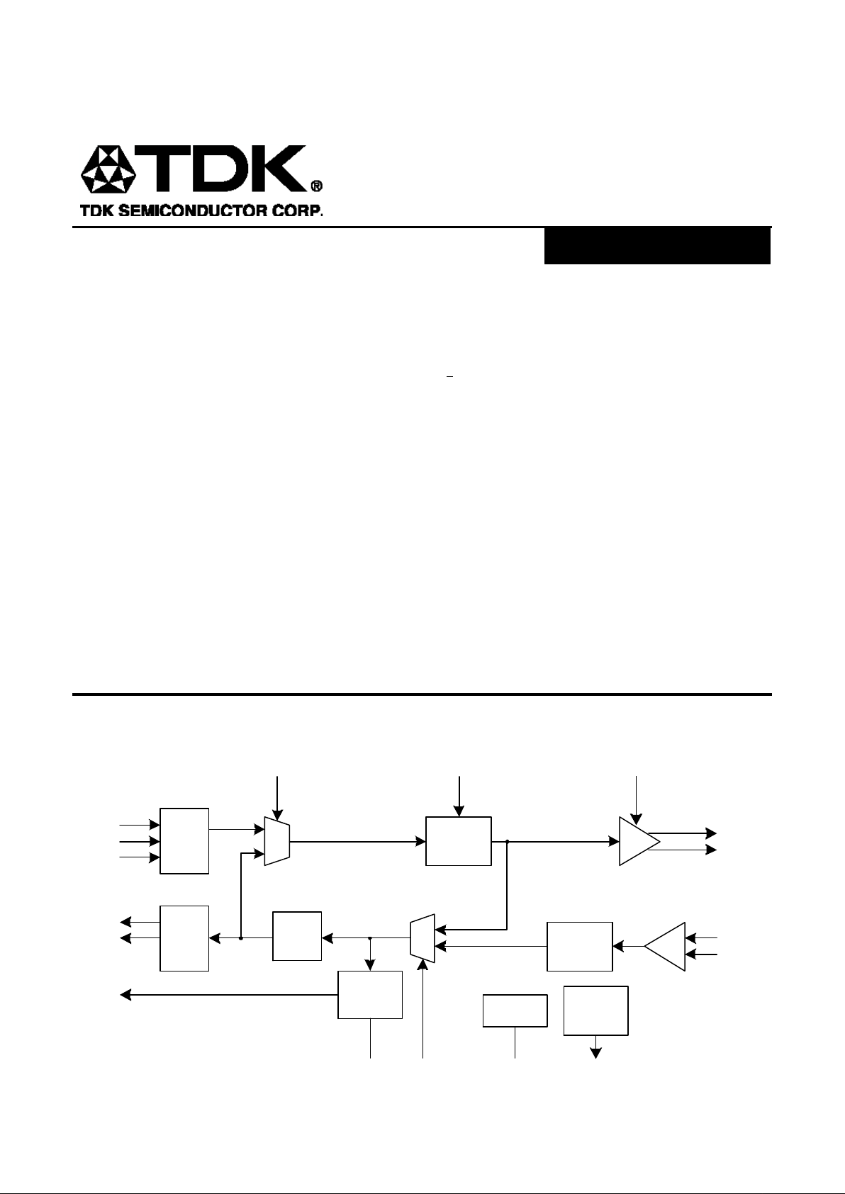
BLOCK DIAGRAM
Advanced Information
PULSE
SHAPER
Clock
Recovery
Adaptive
Equalizer
Data
Slicer
LOS
LINN
LINP
LOUTN
LOUTP
TPOS
LPBK
LF
Signal
Detector
TNEG
AMI
to
Binary
Binary
to
AMI
TCLK
RCLK
RPOS
RNEG
Biasing
RFO
LPBK
LBO
TXEN
78P7200L
E3/DS3/STS-1
Transceiver
2
FUNCTIONAL DESCRIPTION
The 78P7200L is a single chip line interface IC
designed to work with a 51.84 Mbit/s STS-1, 44.736
Mbit/s DS3 or 34.368 Mbit/s E3 signal. The receiver
recovers clock, positive data and negative data from
an Alternate Mark Inversion (AMI) signal. The AMI
line input signal should be B3ZS or HDB3 coded.
The transmitter accepts clock, positive, and negative
data and converts them into an AMI signal to drive a
75Ω coaxial cable. The shape of the transmitted
signal though any cable length of 0 to 450 feet complies
with the published templates of ANSI T1.102-1993,
Telcordia TR-NWT-000499 and GR-253-CORE, ITU-T
G.703. The 78P7200L is designed to work with B3ZS
or HDB3 coded signals. The B3ZS or HDB3 encoding
and decoding functions can be included in the framer
ICs. The 78P7200L is designed to easily connect to
popular ATM framer ICs such as PMC 7345 (SUNI-
PDH), PMC 7346 (QJET) and 7321.
OPERATION SPEED
Internal bias generators that are adjusted by the value of
the RFO set the 78P7200L PLL center frequency and
Transmitter amplitude for the different standards. The E#
pin controls the equalizer response and the transmitter
pulse shape and amplitude. The following table shows
the proper settings.
STANDARD
RFO VALUE,
KΩ
E# PIN SETTING
E3 6.81 Low
DS3 5.23 High
STS-1 4.53 Float
RECEIVER
The receiver input can be either transformer-coupled
or capacitor coupled to the AMI signal. In
applications where the highest performance and
isolation is required, a 1:1 transformer is used on the
receiver path. In the applications, where isolation is
provided elsewhere in the circuit, an AC coupling
can be used. The inputs to the IC are internally
referenced to Vcc. Since the input impedance of the
78P7200L is high, the AMI line must be terminated
to 75 Ω. The input signal of the 78P7200L must be
limited to a maximum of three consecutive zeros
using a coding scheme such as B3ZS or HDB3.
The AMI signal first enters an equalizer and AGC
gain stage. The equalizer is designed to overcome
intersymbol interference caused by long cables.
Because the equalizer is adaptive, the circuit will work
with all square shaped signals such as DS3 high or 34
Mbit/s E3. The variable gain differential amplifier
maintains a constant voltage level output regardless
of the input voltage level. The gain of the amplifier is
adjusted by detecting the peak of the signal and
comparing it to a fixed reference.
Outputs of the data comparators are connected to
the clock recovery circuits. The clock recovery
system employs a phase locked loop with an
auxiliary frequency-sensitive acquisition loop. This
system permits the loop to independently lock to the
frequency and phase of the incoming data stream
without the need for an external, high precision
tuned circuits or reference clock signal.
The jitter tolerance of the 78P7200L meets the
requirements of Telcordia GR-499-CORE for
Category I equipment for DS3 rates and exceeds the
requirements of ITU-T G.823 for E3 rates.
78P7200L
E3/DS3/STS-1
Transceiver
3
FUNCTIONAL DESCRIPTION (continued)
LOSS OF SIGNAL
Should the input signal fall below a minimum value,
the loss of signal indication, LOS goes low.
TRANSMITTER
The transmitter accepts logic level clock (TCLK),
positive data (TPOS) and negative data (TNEG)
signals and generates current pulses on the LOUT+
and LOUT- pins. When properly connected to a
center-tapped 1:2 transformer, an AMI pulse is
generated which can drive a 75 Ω coaxial cable.
When the recommended transformer is used and the
E# pin is set high, the transmitted pulse shape at the
end of the 75Ω terminated cable of 0 to 450 feet will
fit the DS3 template in ANSI T1.102-1993 and
Telcordia GR-499-CORE standard documents.
For STS-1 applications, the transmitted pulse for a
short cable meets the requirements of TelcordiaGR253-CORE. The E# pin should be allowed to float.
For E3 applications, the transmitted pulse for a short
cable meets the requirements of ITU-T G.703. The
E# pin is to be pulled low.
RCLK/TCLK POLARITY REVERSAL:
To simplify the interface with framer circuitry, RCLK
and TCLK can be inverted with the ICKP pin.
PIN 10
ICKP
RCLK TCLK
Low Normal Normal
Float Invert Invert
High Normal Invert
LOOP-BACK MODES:
The following loop-back modes allow for the
diagnostic test of the PC board. This function is
controlled by the LPBK pin.
PIN 40/TQFP
PIN 28/PLCC
LPBK
LOOP-BACK
Low Local loop-back (LLB)
Float Remote loop-back (RLB)
High Normal Operation
LOCAL LOOP-BACK:
When LPBK is low, the 78P7200L enters Local
loopback. In this mode, the LOUT+/- transmit signals
are internally routed to the receiver input circuit. The
incoming line receiver AMI signal on LIN+/- is
ignored. With the transmitter still tied to the cable,
this test mode can indicate a short circuit on the
transmitter external components or other problem in
the transmit path.
REMOTE LOOP-BACK:
When LPBK pin is allowed to float, the 78P7200L
enters remote loopback mode. The RPOS/RNEG
and RCLK pins are internally tied to the
TPOS/TNEG and TCLK so the same AMI signal that
is received by the framer is transmitted back to the
far end where a bit continuity test can be performed.
LINE BUILD-OUT:
The Line Build-Out function controls the amplitude in
DS3 and STS-1 mode. The selection of LBO
depends on the amount of cable the transmitter is
connected to. When used with less than 225 ft of
cable the LBO pin should be pulled high. With 225ft
or more cable the LBO pin should be low.

78P7200L
E3/DS3/STS-1
Transceiver
4
PIN DESCRIPTION: THE 28-PIN PLCC IS COMPATIBLE WITH 78P7200 AND 78P2241
NAME PIN
TQFP
PIN
PLCC
TYPE DESCRIPTION
LIN+
LIN-
42
44
1
3
I Line Input: Differential AMI inputs to the chip. Should be
transformer coupled and terminated at 75-ohm resistor.
RCLK 33 23 O Receive Clock: Recovered receive clock.
RPOS/
RNRZ
35 25 O Receive Positive Data / NRZ Data: This pin indicates
reception of a positive AMI pulse on the coax cable.
RNEG 34 24 O
Receive Negative Data: This pin indicates reception of a
negative AMI pulse on the coax.
LOS
39 27 O Loss of Signal: logic low indicates that receiver signal
(LIN±) is below the threshold level
RPOS and RNEG are forced low when LOS=0.
LOUT+
LOUT-
9
11
9
11
O Line Out: Differential AMI Output. Requires a 2:1 center
tapped transformer and 301Ω resistor.
TCLK 18 16 I Transmitter Clock Input: This signal is used to latch the
TPOS/TNRZ and TNEG signals into the 78P7200L.
TPOS/
TNRZ
16 14 I
Transmit Positive Data / Transmit NRZ: A logic one on this
pin generates a positive AMI pulse on the coax. This pin
should not be high at the same time that TNEG is high.
TNEG 17 15 I
Transmit Negative Data: A logic one on this pin generates
a negative AMI pulse on the coax. This pin should not be
high at the same time that TPOS/TNRZ is high.
LBO 13 12 I Line Build-Out, Transmitter: Logic low used with 225ft or
more of cable is used on transmit path. Logic high used
with less than 225ft of cable.
E#
15 13 I3
DS3, E3 and STS-1 Select: Set low for E# applications.
Set high for DS3, allow to float for STS-1 operation.
Formerly OPT! on the 78P7200.
TXEN 22 18 I Transmitter Enable: When high, enables transmitter.
When low, tri-states transmitter drivers, LOUT±. This pin
was called OPT@ on 78P7200.
ICKP 10 10 I3 Invert Clock Polarity: When low, the polarities of RCLK and
TCLK are the same as those on the 78P7200. When set
high, the polarity of TCLK is inverted. When allowed to float,
the polarities of both RCLK and TCLK are inverted.
LPBK
40 28 I3 Loop-back Select: When high, neither loop-back is
activated.
When allowed to float RPOS, RNEG and RCLK are
looped back onto TPOS, TNEG and TCLK. When low,
LOUT± is looped back onto LIN±.
VCC 5,6,20,
21,37,38
7,17,26 P Power Supply.
N/C 27, 28 20, 21 No Connect

78P7200L
E3/DS3/STS-1
Transceiver
5
PIN DESCRIPTION: THE 28-PIN PLCC IS COMPATIBLE WITH 78P7200 AND 78P2241(continued)
NAME PIN
TQFP
PIN
PLCC
TYPE DESCRIPTION
GND 1, 3, 4, 7, 8,
12, 14, 19, 23,
24, 25, 29, 30,
31, 32, 36, 41,
43, 45, 46, 47,
48
2, 4, 6, 8,
22
P Ground. Connecting all ground pins to a common ground
plane is recommended.
RFO 2 5 - A resistor to GND sets the operational speed of the chip.
RFO= 5.23K for DS3, RFO=6.81K for E3 and
RFO=4.53K for STS-1.
LF1 26 19 - Receiver PLL filter capacitor.
Note 1: Pin type: I-input; I3-three level logic input; O-output; P-power supply. Advanced Data sheet pin
assignment and functions are subject to change.
78P7200L
E3/DS3/STS-1
Transceiver
6
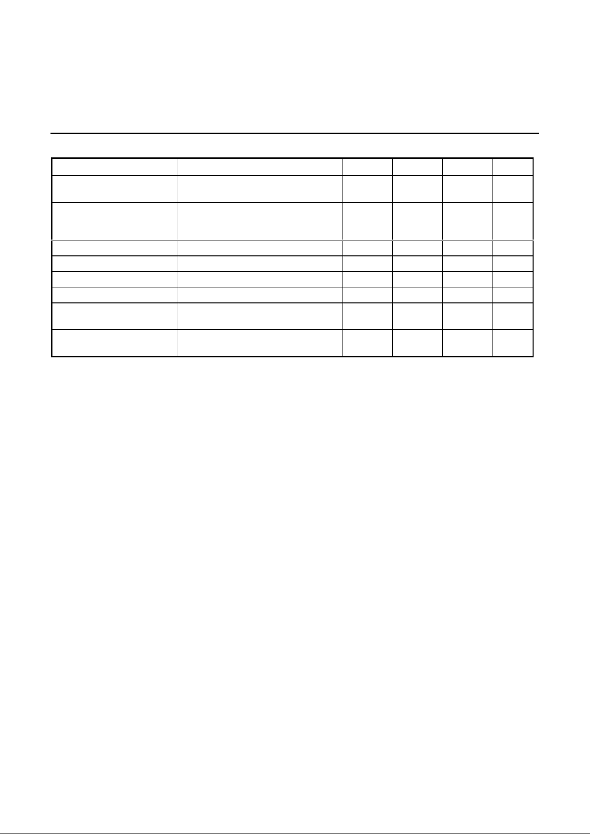
ELECTRICAL SPECIFICATIONS
ABSOLUTE MAXIMUM RATINGS
Operation beyond these maximums rating may permanently damage the device .
PARAMETER RATING
Positive supply, V
CC
6V
Storage temperature -65 to 150
Ambient operating temperature
-40 to +85 °C
Output Pin Voltage (LOUT+, LOUT-)
Input Pin Voltage (LIN+, LIN-)
VCC -2 to VCC +2 V
Input pin voltage, all other pins
VCC+0.3 to
GND
-0.3 V
DC CHARACTERISTICS: Ta = -40 ° to +85°C; positive supply voltage = 5V ±0.5V or 3.3V±0.3V
PARAMETER PIN TYPE CONDITION MIN TYP MAX UNIT
Supply current I
CC
Transmit and receive all
ones, VCC=5V or 3.3V
70 95 mA
Supply current I
CC
transmitter disabled,
TXEN=0
35 mA
V
IL
I 0.8 V
V
IH
I 2.0 V
IIL, I
IH
I -10 +10 uA
V
IL3
I3 0.5 V
Z
IM3
I3 Input Floating 8 10 20
kΩ
V
IH3
I3
VCC-0.5
V
I
IL3
, I
IH3
I3 -100 +100 uA
V
OL
O
IOL=-0.1mA
0.5 V
V
OH
O
IOL=+0.1mA VCC-0.5
V
78P7200L
E3/DS3/STS-1
Transceiver
7
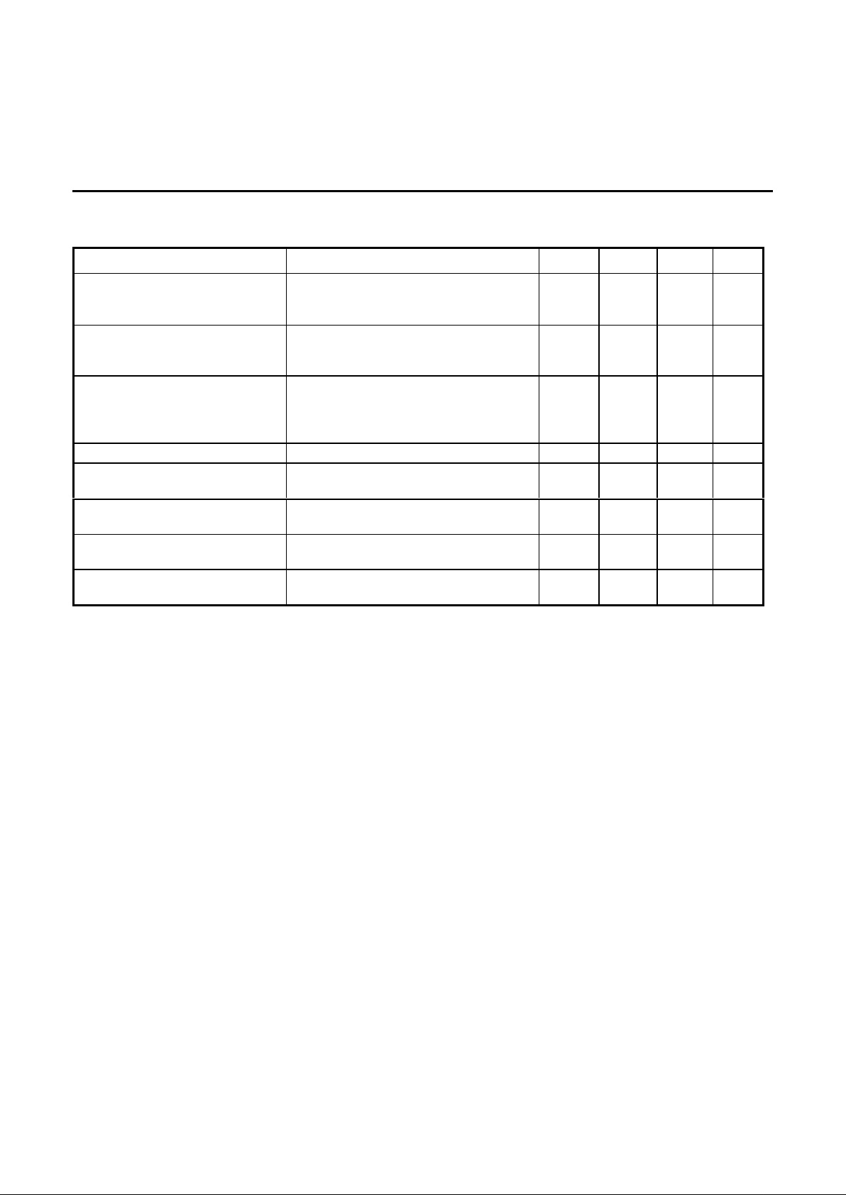
E3 – receiver (RFO = 6.81k Ω, E# is set low), receiver is transformer-coupled.
PARAMETER CONDITION MIN TYP MAX UNIT
Peak Differential Input
Amplitude, LIN+, LIN-
See Note 2 104 1200
mV
pk
Bit Error Ratio in the
presence of an Interfering
Signal at Receive Input
Interfering signal power 20dB below
E3 signal power. Both are PRBS23
(223-1) patterns.
10
-9
RCLK rise/fall time TRCT 2 4 ns
RCLK period, TRCF 29.10 ns
RCLK clock duty cycle 45 55 %
RCLK pulse width TRC 14.55 ns
RPOS/RNEG data setup
time TRDPS
CL=15 pF 7 ns
RPOS/RNEG data hold
time TRDPH
CL=15 pF 7
Note 2: 104 mV
pk
equals 950 mVpk at the source with 1100 feet of cable (13.2dB loss).
78P7200L
E3/DS3/STS-1
Transceiver
8
DS3/STS-1 RECEIVER (RFO = 5.23KΩ FOR DS3 AND 4.53KΩ FOR STS-1, E# PIN IS SET HIGH OR
ALLOWED TO FLOAT), INPUT IS TRANSFORMER COUPLED
PARAMETER CONDITION MIN TYP MAX UNIT
Peak Differential Input
Amplitude, LIN+ and LIN(see Note 3)
Signal at DSX is 360-850mVP (see
Note 4)
90 850 mVP
Peak Differential Input
Amplitude, LIN+ and LIN-
DS3 HIGH (see Note 5) 90 1200 mVP
Bit Error Ratio in the presence
of an Interfering Signal (IS) at
LIN+,LIN-
IS is a sinusoidal tone, 22.368 MHz
for DS3 or 25.92MHz for STS-1. Data
is a PRBS15 (215-1) pattern. IS power
is 10dB below data signal power.
10
-9
RCLK rise/fall time TRCT Cl=25pf 5 ns
RCLK period
TRCF
DS3
STS-1
22.35
19.29
ns
RCLK pulse width
TRC
DS3
STS-1
12.24
9.65
ns
RPOS/RNEG data setup time
TRDPS
CL=15 pF 7 ns
RPOS/RNEG data hold time
TRPDH
CL=15 pF 7 ns
Note 3: Signal source should meet DS3 template of ANSI-T102.1993 Figure 4 and STS-1 template of ANSIT102.1993 Figure 5, Loss characteristics of the WE728A or RG 59B cable should be better than Figure C2 of
ANSI-T102.1993.
Note 4: Receiver can handle up to 450 feet of cable loss (5.5dB) from the DSX cross-connect.
Note 5: Case where test signal is fed directly into receiver with fast rise times violates DS3 template and normal
maximum. Interfering signal performance is not guaranteed in the presence of DS3 High at the input ..
 Loading...