

TDK Semiconductor Corporation 78P2253-IGT Datasheet
DESCRIPTION
78P2253
E4/STM-1/STS-3/OC-3
Transceiver
Advanced Information
November 2000
FEATURES
The 78P2253 is a transceiver IC designed for
139.264Mbit/s (E4) or 155.52Mbit/s (OC-3, STS-3 or
STM-1) transmission. It is used at the interface to a
75Ω coaxial cable using CMI coding or a fiber optic
module. Interface to digital framer circuits is
accomplished via a serial PECL or parallel CMOS
interface.
The transmitter includes a PLL to multiply the
reference clock to the transmission frequency. The
receiver provides adaptive equalization for accurate
clock and data recovery. The 78P2253 is built in a
BiCMOS technology for high performance and low
power operation. It operates with a 3.3V or 5V power
supply and is packaged in a 64-pin TQFP.
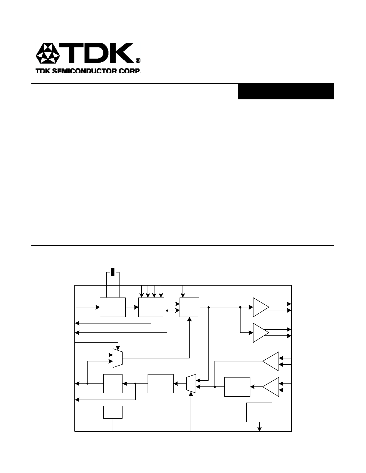
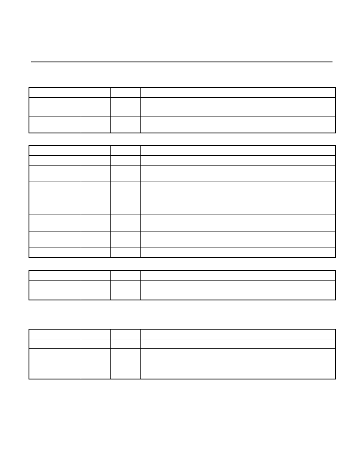
BLOCK DIAGRAM
$BIT
SER
HOST
SONET
XTAL1
XTAL2
HUB/
PAR/
8BIT/
E4/
• 139.264Mbit/s or 155.52Mbit/s interface for
CMI coded transmission using 75Ω coaxial
cable
• Compliant with ITU-T G.703, G.823 jitter
tolerance, Telcordia TR-NWT-00253
• Integrated Clock Recovery Unit (CRU)
• Serial PECL Interface
• Four and Eight bit Parallel CMOS Interfaces
• PECL Interfaces for connection to Fiber
Optic Modules for SONET OC3 applications
• Adaptive Equalization
• Integrated Clock Multiplier PLL
• Advanced BiCMOS Process
ECL
CMI/
CKIN
TXCK
TXCKP,N
RLBACK
TXDTP,N
TXDT[7:0]
RXDTP,N
RXDT[7:0]
RXCKP,N
RXCK
Crystal
Oscillator
CMI to
Binary
Bias
RFO
Clock
Generator
Clock
Recovery
LF
Binary
to CMI
BACK
LL
Adaptive
Equalizer
CMIOUTP
CMIOUTN
ECLOUTP
ECLOUTN
ECLINP
ECLINN
CMIINP
CMIINN
Signal
Detector
LOS
78P2253
E4/STM-1/STS-3/OC-3
Transceiver
FUNCTIONAL DESCRIPTION
The 78P2253 contains all the necessary transmit
and receive circuitry for connection between
139.264Mbit/s or 155.52Mbit/s signals and digital
Framer/Deframer ICs.
Operating Rate
The 78P2253 has a variety of operating modes and
rates. They are summarized in the tables below.
More detailed descriptions can be found in the
sections that follow.
Standard E4/SONET CMI/ECL Rate
(Mbit/s)
OC-3
STM1 optic
STS-3
STM-1 Coax
E4 1 1 139.264 17.408 CMI
0 0 155.52 19.44 ECL
0 1 155.52 19.44 CMI
1 0 139.264 17.408 ECL
The digital interface of the 78P2253 can be either
Serial PECL, 4-bit Parallel CMOS or 8-bit Parallel
CMOS.
Mode
Serial 0 X TXDTP,N
Parallel
Parallel
PAR/SER 8BIT/BIT
4-bit
8-bit
1 0 TXDT[3:0]
1 1 TXDT[7:0]
Data pins
RXDTP,N
RXDT[3:0]
RXDT[7:0]
Transmit timing is derived from either the reference
clock (the crystal oscillator or CKIN), or the
recovered receive clock. LLBACK and RLBACK
control the local and remote loopback modes
respectively.
LLBACK RLBACK HUB/HOST Transmit Clock derived from
0 0 1 Reference
1 0 1 Reference
X 1 1 Receiver
X X 0 Receiver
Medium Choices
The CMI/ECL pin selects one of two media for
transmission.
When the CMI/ECL pin is high, the chip is in CMI
mode and a 75Ω coaxial cable is used as the
transmission medium. In this mode, the CMIOUTP
and CMIOUTN pins are active. They connect the
chip to the coaxial cable through a transformer and
Reference
Frequency
(MHz)
Clock
pins
TXCKP,N
RXCKP,N
TXCK
RXCK
TXCK
RXCK
Active I/O
Clock
Frequency
(MHz)
155.52(Sonet)
139.264 (E4)
38.88(Sonet)
34.816(E4)
19.44(Sonet)
17.408(E4)
matching resistors. In CMI mode the transmitter
shapes the transmit pulses to meet the appropriate
template and the adaptive equalizer corrects the
received signal for dispersive attenuation. The
ECLOUTP and ECLOUTN pins are inoperative and
should be left open.
When the CMI/ECL pin is low the chip is in ECL
mode and a fiber optics transceiver is used. The
output data signal from the pins ECLOUTP and
ECLOUTN have PECL levels. In this mode, the CMI
pins are inoperative and should be left open. The
CMI encoder and decoder are disabled.
TRANSMITTER OPERATION
The transmitter section generates an analog signal
for transmission through a transformer onto the
coaxial cable or fiber optic module.
When the PAR/SER pin is low the chip is in serial
mode. Serial data is input to the 78P2253 on the
TXDTP and TXDTN pins at PECL levels. The data is
timed with the clock generated by the 78P2253 on
the TXCKP and TXCKN pins. In this mode the
8BIT/$BIT pin is ignored.
When the PAR/SER pin is high the chip is in parallel
mode. Parallel data is in put to the 78P2253 on the
TXDT[7:0] pins. The input data is timed with the
clock output from TXCK. When 8BIT/ $BIT is high all
eight bits of TXDT[7:0] are used and the clock
frequency at TXCK is one-eighth the standard
frequency. When 8BIT/$BIT is low the lower four
bits, TXCK[3:0] are used and TXCK is one-fourth the
standard frequency.
The first bit output from the ECL/CMI interface is the
most significant bit on the parallel interface, TXDT7
in eight bit mode, TXDT3 in four bit mode.
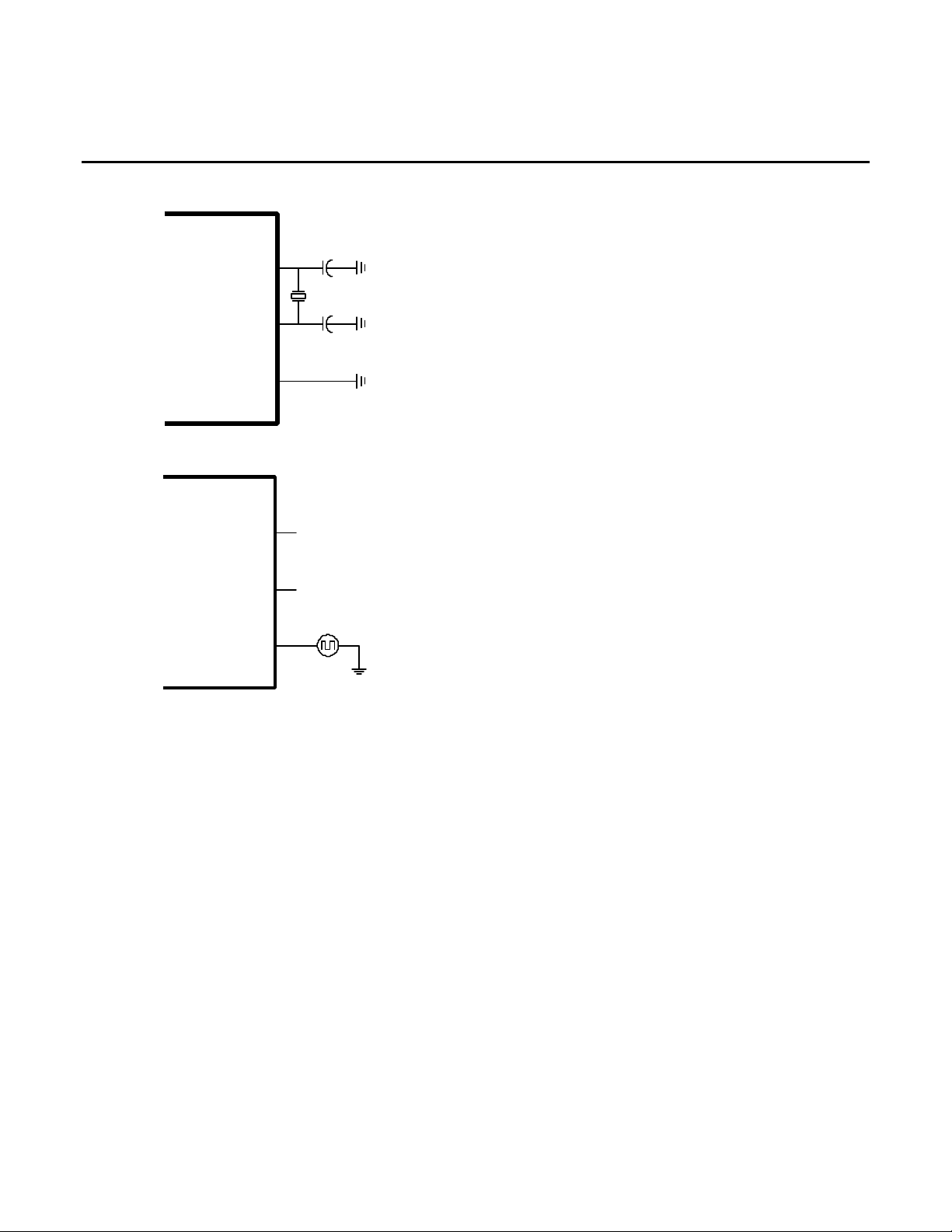
The clock is generated by a phase-locked oscillator
(PLO). The PLO is locked to a crystal oscillator
operating at one-eighth of the standard clock
frequency, 19.44MHz for OC-3, STS-3 and STM-1
and 17.408MHz for E4. This is shown in Figure 1a.
An external clock signal at CKIN may also be
substituted for a crystal as the reference frequency
for the chip. In this mode, XTL1 and XTL2 must be
configured as shown in Figure 1b. Note that the chip
can be in either ECL or CMI mode when using either
an external clock or a crystal for the reference. In
serial mode the reference clock is output from
TXCK. In parallel mode, the parallel transmit clock is
output from TXCK.
2
78P2253
E4/STM-1/STS-3/OC-3
Transceiver
TRANSMITTER OPERATION (continued)
XTAL1
XTAL2
CKIN
FIGURE 1A : USING CRYSTAL
XTAL1
XTAL2
17.283 MHz (E4)
19.440 MHz (Sonet)
CKIN
FIGURE 1B: USING EXTERNAL CLOCK
In ECL mode the data signal is converted to CMI
code by the Binary to CMI encoded.
The HUB/HOST input changes the reference signal
for the clock generator. In the hub mode (HUB/HOST
high), the transmit clock reference is derived from
either the crystal oscillator or CKIN. In host mode
(HUB/HOST low), the transmit clock reference is
derived from the recovered receive clock.
RECEIVER OPERATION
The receiver accepts serial, CMI coded data, at
155.52Mbit/s or 139.264Mbit/s from either the CMI
or the ECL inputs. In CMI mode, the inputs CMIINP
and CMIINN receive the input signal from a coaxial
cable that is transformer-coupled to the chip. The
ECL pins should be left open. In ECL mode, the pins
ECLINP and ECLINN receive the input signal.
In CMI mode, the received signal is equalized for
dispersive cable attenuation and decoded in the CMI
to binary decoder.
A clock signal is recovered using a low jitter PLL
circuit.
The data is converted to binary by the CMI to Binary
decoder.
In serial mode, the received data is output on the
RXDTP and RXDTN pins and the recovered clock is
output on the RXCKP and RXCKN pins.
In parallel mode, the received data is converted to
parallel, eight bits if 8BIT/ $BIT is high and four if it is
low. The first bit received will arrive on the most
significant output pin, RXDT[7] in eight bit mode and
RXDT3 in four bit mode.
The LOS pin goes high when the signal detector
detects a loss-of-signal condition.
LOOPBACK OPERATION
The 78P2253 is capable of performing signal
loopback in two ways The RLBACK pin selects the
remote loopback mode. In this mode, the received
signal is “looped back” and sent out of transmitter in
place of the transmit input signal.
The LLBACK pin selects the local loop-back mode,
and causes the receiver to use the transmitter output
signal as its input. Local loopback is disabled when
HUB/HOST is low or RLBACK is high.
3
78P2253
E4/STM-1/STS-3/OC-3
Transceiver
PIN DESCRIPTION
LEGEND
TYPE DESCRIPTION TYPE DESCRIPTION
A Analog Pin PI PECL Digital Input
CI CMOS Digital Input PO PECL Digital Output
CO CMOS Digital Output S Supply Pin
TRANSMIT PINS
NAME PIN TYPE DESCRIPTION
TXDTP
TXDTN
TXCKP
TXCKN
TXDT[7:0] 11-18 CI Transmit Data Inputs – Parallel Mode. TXDT[7:4] are ignored in 4 bit
TXCK 10 CO Reference Clock Output – Serial mode.
CMIOUTP
CMIOUTN
ECLOUTP
ECLOUTN
19
20
22
23
60
59
56
55
PI Transmit Data Inputs - Serial Mode.
PO Transmit Clock Output - Serial Mode.
mode.
Transmit Clock Output – Parallel Mode.
A Transmit Output in CMI mode.
No signal is output in ECL mode.
PO
Transmit Outputs for ECL mode.
No signal is output in CMI mode.
RECEIVE PINS
NAME PIN TYPE DESCRIPTION
CMIINP
CMIINN
ECLINP
ECLINN
RXCKP
RXCKN
RXCK 38 CO Recovered Receive Clock – Parallel Mode.
RXDTP
RXDTN
RXDT[7:0] 30-37 CO Receive data – Parallel Mode. In 4 bit mode RXDT[3:0] are used and
50
49
52
51
25
26
27
28
A Receive inputs in CMI mode.
Transformer coupled from the coaxial cable.
Ignored in ECL mode.
PI Receiver inputs in ECL mode.
Ignored in CMI mode.
PO Recovered Receive Clock – Serial Mode.
PO Receive data – Serial Mode.
RXDT[7:4] are pulled low.
4
78P2253
E4/STM-1/STS-3/OC-3
Transceiver
PIN DESCRIPTION (continued)
REFERENCE CLOCK PINS
NAME PIN TYPE DESCRIPTION
XTAL1
XTAL2
CKIN 9 CI Reference clock input. The crystal oscillator connections should be
CONTROL AND STATUS PINS
NAME PIN TYPE DESCRIPTION
RLBACK 41 CI Loopback receiver output to transmitter input.
LLBACK 42 CI
HUB/HOST 2 CI In HUB mode (input high) the transmit reference clock is derived from
CMI/ECL 1 CI Selects CMI (input high) or ECL (input low) modes.
E4/SONET 64 CI When high, E4 (139.264 Mbit/s) operation is selected. When low,
8BIT/$BIT CI Selects 8 bit parallel data when high and 4 bit parallel mode when
LOS 39 CO High during a loss-of-signal condition.
5
6
A Crystal Pins. Connect as in Figure 1a.
left open.
Loopback transmitter output to receiver input. Disabled when
HUB/HOST is low or RLBACK is high.
the CKIN pin or the crystal oscillator. In HOST mode (input low) the
transmit reference clock is derived from the recovered receive clock.
STM-1/STS-3/OC-3 (155.52Mbit/s) operation is selected.
low. In serial mode this pin is ignored.
ANALOG PINS
NAME PIN TYPE DESCRIPTION
RFO 46 A External reference resistor.
LF 44 A PLL loop filter capacitor.
POWER SUPPLY PINS
It is recommended that all VCC pins be connected to a single power supply plane and all GND pins be connected
to a single ground plane.
NAME PIN TYPE DESCRIPTION
VCC 43 S Power Supply.
GND 4, 7, 21,
29, 45,
47, 48,
58, 61
S Ground.
5
78P2253
E4/STM-1/STS-3/OC-3
Transceiver
ELECTRICAL SPECIFICATIONS
ABSOLUTE MAXIMUM RATINGS
Operation beyond these limits may permanently damage the device.
PARAMETER RATING
Supply Voltage 7 VDC
Storage Temperature -65 to 150° C
Pin Voltage -0.3 to (VCC+0.3) VDC
Pin Current
RECOMMENDED OPERATING CONDITIONS
Unless otherwise noted all specifications are valid over these temperatures and supply voltage ranges.
PARAMETER RATING
DC Voltage Supply, VCC
Ambient Operating Temperature -40 to 85°C
DC CHARACTERISTICS:
PARAMETER SYMBOL CONDITIONS MIN NOM MAX UNIT
Supply Current (Parallel Mode) Icc Vcc = 3.3V
Supply Current (Serial Mode) Icc VCC = 3.3V
±100 mA
3.3 ± 0.3 VDC; 5 ± 0.5 VDC
Vcc = 5.0V
VCC = 5.0V
140
150
210
280
165
175
245
330
mA
mA
DIGITAL INPUT CHARACTERISTICS
Pins of type CI
PARAMETER SYMBOL CONDITIONS MIN NOM MAX UNIT
Input Voltage Low Vil 0.8 V
Input Voltage High Vih 2.0 V
Input Current Iil, Iih -10 10
Input Capacitance Cin 10 pF
Pins of type PI
PARAMETER SYMBOL CONDITIONS MIN NOM MAX UNIT
Input Voltage Low Vil Relative to Vcc -1.5 V
Input Voltage High Vih Relative to Vcc -1.1 V
µA
6
78P2253
E4/STM-1/STS-3/OC-3
Transceiver
ELECTRICAL SPECIFICATIONS (continued)
DIGITAL OUTPUT CHARACTERISTICS
Pins of type CO
PARAMETER SYMBOL CONDITIONS MIN NOM MAX UNIT
Output Voltage Low Vol Iol = 2mA 0.6 V
Output Voltage High Voh Ioh = -2mA Vcc –
0.6
Transition Time Tt 3.5 ns
Pins of type PO
PARAMETER SYMBOL CONDITIONS MIN NOM MAX UNIT
Output Voltage Low Vol Relative to Vcc -1.8 -1.6 V
Output Voltage High Voh Relative to Vcc -1.1 -0.8 V
Rise Time Tr 1 ns
Fall Time Tf 1 ns
V
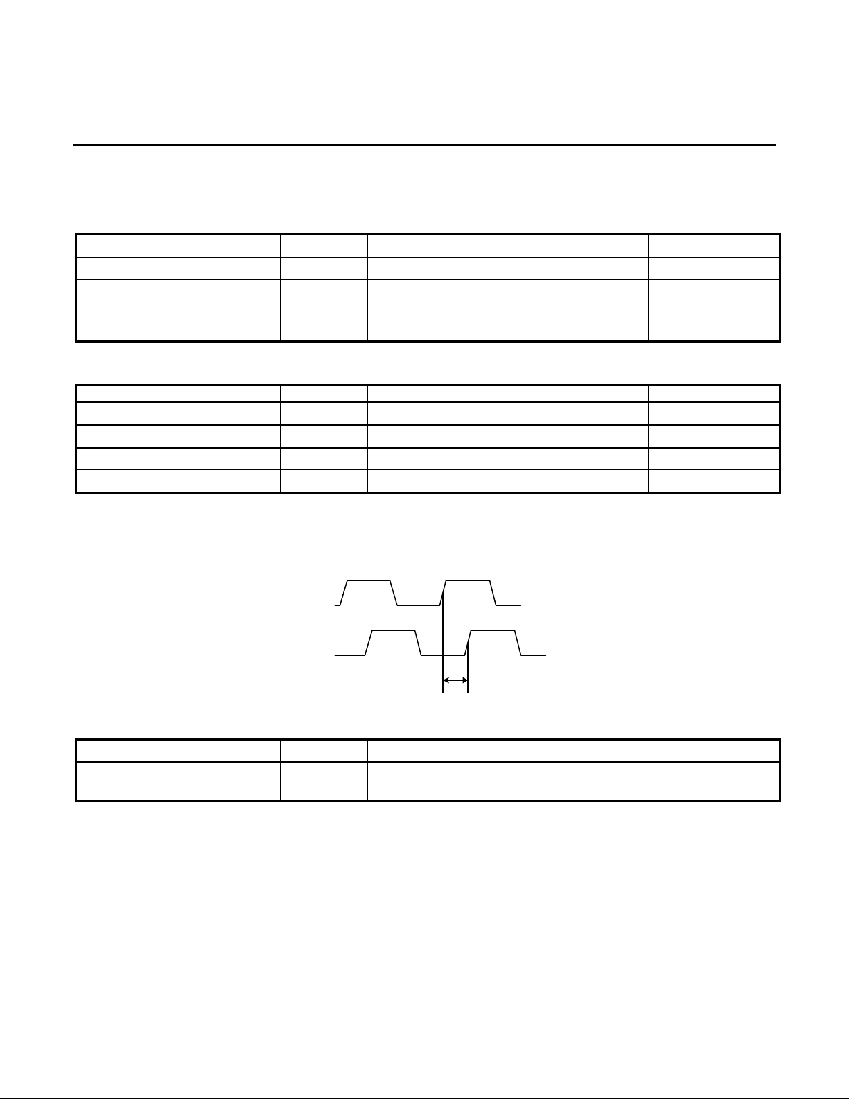
DIGITAL TIMING CHARACTERISTICS:
Reference Clock Interface
CKIN
TXCK
T
CK
PARAMETER SYMBOL CONDITIONS MIN NOM MAX UNIT
CKIN to TXCK Propagation
Delay
T
CK
20 ns
7
 Loading...