

TDK Semiconductor Corporation 73M2921-LG Datasheet

Rev M
Advanced Information
73M2921
Advanced Single
Chip Modem
February 1999
DESCRIPTION
The 73M2921 is a CMOS integrated circuit which
provides all the modem “Data Pump” functions
required to implement a V.22bis data modem. It
consists of a DSP (Digital Signal Processor) core
with RAM and ROM data memor y, ROM instruction
memory, and register ma pped input/output functions
including timers, interrupts, Σ∆ ADC and DAC ports
and Serial Data I/O.
Once the 73M2921 has been initialized, all call
progress and modem handshaking is automatic.
The default conditions may be cha nged as required
for country specific or custom applications.
The 73M2921 provides DTMF tone generation and
detection, precise call progress detect and ADSI
functions such as CAS tone detection.
Other features include a parallel interface control
port between the host pr ocessor and the 73M2921.
A synchronous serial data channel provides
synchronizing clocks RXCLK and TXCLK from the
modem pump to the controller.
The 73M2921 contains an oscillator and power
control features.
The host controller function can be implemented with
a 73M2910 communications micro controller or
another commercial microcontroller (such as the
68302). The 73M2921 has been optimized to work
with the 73M2910 synchronous serial port.
FEATURES
• Automatic handshaking for all data modes
• Data Speeds:
V.22bis - 2400 b/s
V.22, Bell 212 - 1200 b/s
V.21, Bell 103 - 300 b/s
V.23 1200 b/s - 75 b/s
Bell 202 1200 b/s
• Facsimile Speeds:
V.29 - 9600, 7200 b/s
V.27ter - 4800, 2400 b/s
V.21 ch 2 - 300 b/s
• V.8bis applications
• Designed for 3.3 and 5-Volt systems.
• Low operating power.
• Speaker monitor output
• Provides 2 tone generators for single tone or
DTMF generation
• Provides DTMF tone detection
• Provides 4 precise and 1 imprecise call
progress filters and corresponding detect
bits with programmable thresholds and
frequencies
• Provides CAS tone detection for ADSI and
CLASS feature support
• Supports parallel (8 bit) control, and
synchronous serial data I/O
• 73M2921 provides a microcontroller inter-
rupt
• Packaging: The 73M2921 is available in a
QFP production package. A PGA package is
available for prototyping
73M2921
Advanced Single
Chip Modem
Page 2 of 41 TDK Semiconductor February 99 Rev M
FIGURE 1 - Block Diagram
P
PORT
CR0
MAILBOX
READ THE
MAILBOX
RAM/
ROM
VOLT AGE
REFERENCE
SERIAL
DATA
POWER
UP
DSP
CLOCKS
TIMER
(MODULATOR & DECIMATOR)
(ADC &DAC)
SERIAL CLOCKS
14.4 KHz Samples
CTRL
XTALI
XTALO
CLK CTRL
MICCLK
RESET
PWR UP
INTERRUPTS
TXDRXD TXCLK RXCLK
CLK CNTRL
DIGITAL
BIT STREAM
MON
INPA
INNA
OUTPA
OUTNA
ANALOG
VBG
VREF
PWR UP
UA[0-1]
UD[0-7]
,
VPD VPA VND VPA
73M2921
Advanced Single
Chip Modem
February 99 Rev M TDK Semiconductor Page 3 of 41
PIN DESCRIPTION
POWER
NAME PIN TYPE DESCRIPTION
VPD 3, 23,
51, 82
I DIGITAL POWER: Positive Digital Power.
VND
4, 20,
52, 74
I DIGITAL POWER: Negative Digital Power.
VPA 29, 36 I ANALOG POWER: Positive Analog Power.
VNA 27, 37 I ANALOG POWER: Negative Analog Power.
VREF 32 O
VREF: Analog voltage referen ce for biasing of off chip analog function.
Maximum output current is +/- 20µA.
VBG 33 O BANDGAP VOLTAG E: Bandgap vo ltage pin used as a connect ion point
for an external capacitor for noise reduction only.
CLOCKS AND RESETS
NAME PIN TYPE DESCRIPTION
XTALI 22 I CRYSTAL INPUT: Onboard crystal oscillator input, or the master cl ock
input to the 73M2921 if the crystal oscillator is not used.
XTALO 21 I CRYSTAL OUTPUT: Onboard crystal oscillator output should be left
unconnected if the cr ystal oscillator o n the 73M2921 is not used. Along
with XTALI and proper loading capacitor s, these pins include an inverter
for use with parallel resonant mode crystals.
MICCLK 19 O MICROCONTROLLER CLOCK: Programmable clock output for use
when the system oscillator is on the 73M29 21. Ma y be u sed to drive t he
system controller. The output frequen cy is controlled by CR0 bits D11D9 (MCLK [2:0]).
RESET 40 I MASTER CHIP RE SET: Active High Input with hysteresis. Resets the
73M2921 and the contro l registers. If not used as a re set source, this
pin must be tied low.

73M2921
Advanced Single
Chip Modem
Page 4 of 41 TDK Semiconductor February 99 Rev M
PIN DESCRIPTION (continued)
POWER CONTROL
NAME PIN TYPE DESCRIPTION
'7,
26 I DATA TERMINAL INTERRUPT 0: Active Low Input with hysteresis.
Power up signal. The a ction of this pin ca n be masked by the PS DIS[1]
register bit. This pin would connect t o EIA-2 32 conne ction DTR in m any
applications. Requir e s a 50KΩ external pu ll up.
5,1* 24 I RING DETECT: Active Low Inpu t with h ystere sis. P ower up signa l. The
action of this pin can b e masked by the PSDIS[0] reg ister bit. This pin
would connect to the r ing detect c ircuitry or the contr ol micr ocontrol ler in
many applications. Requires a 50KΩ external pull up.
:$.( 39 O
WAKE: Active Low Output. Indicates that a power up pin (5,1* or
'7,) has been activated when the 73M2921 is in slave mode. The
latched signal remains true until a reset of the wake function by a write to
CR0 LSByte, or a chip reset. Requires a 50KΩ external pull up.
MICROCONTROLLER INTERFACE
NAME PIN TYPE DESCRIPTION
&6 15 I
CHIP SELECT: Active Low Input. Enables data transfers on the µP
parallel interface. Requires a 50KΩ externa l pull up.
5' 17 I READ: Acti ve Low Input. Read enable sign als for the mailbox/control
register interface.
:5 16 I
WRITE: Active L ow Input. Write en able signals for the mailbo x/control
register interface.
UA[0:1] 13-14 I ADDR ESS: Address bits that are u sed by the µP to communicate with
the 73M2921 mailbox and CR0.
UD [0:7] 5-12 I/O DATA: Parallel data bus for the mailbox/CR0 interface.
8,17
18 O INTERRUPT: µC interrupt Active Low Output. Used as an interrupt to
the microcontroller indicating that the 73M2921 needs data or has a
request for the µC. It is activated when the 73M2921 writes to the
mailbox and cleared wh en the µ C read s the mai lbox LSB yte. Requir es a
50KΩ external pull up.
73M2921
Advanced Single
Chip Modem
February 99 Rev M TDK Semiconductor Page 5 of 41
PIN DESCRIPTION (continued)
SERIAL DATA INTERFACE
NAME PIN TYPE DESCRIPTION
RXCLK 45 O RECEIV E CLOCK: Receive clock for the serial data interfa ce. Data is
transferred from the 73M2921 on the rising edge of the clocks.
TXCLK 42 O
TRANSMIT CLOCK: Transmit clock for the ser ial data inter face. Da ta is
transferred to the 73M2921 on the rising edge of the clocks.
RXD 44 O RECEIVE DATA: Receive Digital Data.
TXD 41 I TRANSMIT DATA: Transmit Digital Data.
AUXILIARY FUNCTIONS
NAME PIN TYPE DESCRIPTION
MON 38 O MONITOR: Speaker driver. PCM output under software control. See
app note concerning the use of this pin.
PEXT 50 I
EXTERNAL PROGRA M ENABLE: This pin must be ti ed low for normal
operation.
ANALOG I/O
NAME PIN TYPE DESCRIPTION
INPA,
INNA
34,
35
I ANALOG INPUT: Differential analog input to a high resolution ADC.
OUTPA,
OUTNA
31,
30
O ANALOG OUTPUT: Differential analog output from a high resolution
DAC.
HARDWARE REQUIREMENTS
The 73M2921 chip is designed for a single +3.3 or 5 Volt supply and for minimum power consumption
(~100mW @ 3.3V). It supports power do wn (i dle) mode via micr ocontr oller sof tware control. It will a ls o ac cept
a request for power down from the DTE via h ardware control. T he device operates from internal ROM/RA M,
but may be configure d for external ROM operati on and external RAM access (for custom applications) using
either the prototype or the production packages.
LINE/HYBRID INTERFACE
The 73M2921 chip provides a diff erential analog input and output. This interface wil l drive a standard Data
Access Arrangement (DAA). The system controller provides additional control such as hook, phone and
auxiliary relay, parallel pickup and in-use detect, and ring detect.
The Internal DAC provides a differential output signal with a maximum output swing of 1.2Vpp, capable of
driving a 50KΩ load. One output can be used alone for a sing le ended output (with possible perf ormance
degradation).
The internal ADC has a diffe rential input maximu m of 1.2Vpp, and provid es a biasing resistor to Vref for AC
coupling. One input can be driven while leaving the other floating for a single ended input (with possible
performance degradation). The signal passes through a passive anti-aliasing filter.
73M2921
Advanced Single
Chip Modem
Page 6 of 41 TDK Semiconductor February 99 Rev M
POWER CONTROL
The power control circuit determine s t he sta te o f th e 73M 2 921 whe n po wer ed down , a nd t he mea ns for wa k ing
up the chip. The function is related to the chi p and DSP r eset functions and is contr olled by vario us input pin s
and register bits. The chip pins are 5,1* '7,, and RESET. The CR0 re gister bits that control power c ircuit
function are RSTCHIP, RSTDSPB, ENOSC, ENDSPCK, ENMCLK, and PSDIS (1:0).
POWER CONTROL CIRCUIT FUNCTION
Power consumption can be reduced by turning off or slowing down specific circuit functions in register CR0.
•
EN DSP=0: stops DSP clock.
•
EN MCLK=0: turns off
u
C clock. MCLK=000: state gives lowest µC clock frequency.
•
EN OSC=0: turns off oscillator and analog bias currents.
•
DSPCK=000: state gives lowest DSP clock frequency.
The 73M2921 has a power-down mode. Access to this mode is described below.
Power Down Mode: To achieve power down first set RSTDSP to 0 in CR0 (b it 0). Second, set ENDSPCK,
ENMCLK, and ENOSC to 0 in CR0 (bits 12, 8, and 7 respectively). Writing a one to ENDSPCK, ENMCLK, and
ENOSC will bring the 73M2921 back to its previous power mode.
Powering up: Toggling the RESET pin, '7,, or 5,1* w ill power the 73M2921 up to Normal mode. Similar
results can be achieved by writing to the reset pin in CR0 (00b, bit 3).
The following is a functionalit y chart for th e power con trol circu itry. It sh ows all inputs and descr ibes the eff ect
on various 73M2921 functions.
INPUT AFFECTED SIGNAL OR FUNCTION
PIN
5,1*
(Pin 24)
'7,
(Pin 26)
These are the two pins used to bring the chip out of a power
down state. Their function can be masked by the PSDIS bits
in register CR0.
CR0 bits
ENDSPCK
(CR0 D12)
ENOSC
(CR0 D7)
Either of these bits in CR0 set to ONE inhibits the generation of a pulse that
will reset the DSP.
PSDIS1
(CR0 D2)
Masks '7, input when set.
PSDIS0
(CR0 D1)
Masks 5,1* when set.
Table 4 - Power Control Functions
73M2921
Advanced Single
Chip Modem
February 99 Rev M TDK Semiconductor Page 7 of 41
POWER CONTROL TIMING
DESCRIPTION MIN TYP MAX UNIT
Powerup input to active state 250 µs
Powerup input to inactive state 50 µs
Table 5 - Power Control Timing
DCE-DTE INTERFACE
The 73M2921 is designed to interface with a synchronous port such as that found on the TDK 73M2910. It also
provides a parallel control interface. This parallel interface appears as an 8 bit memory mapped peripheral to the
host controller.
SERIAL DATA INTERFACE
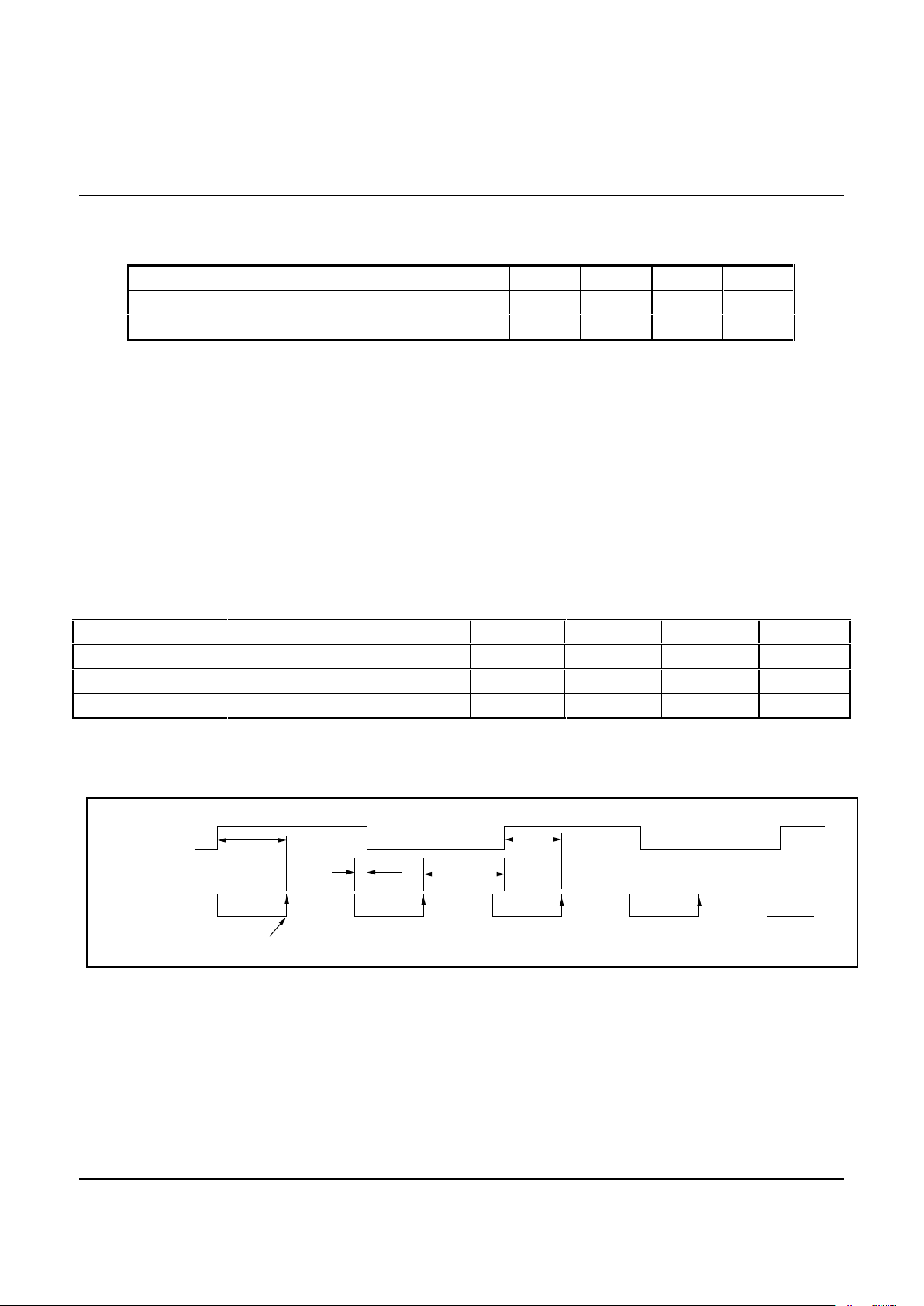
The serial data interface is a four pin bi-directional port. It consists of the TXD and RXD data paths (LSBit
shifted in and out first, respectively), the TXCLK and RXCLK serial clock outputs associated with the data pins.
SYMBOL DESCRIPTION MIN TYP MAX UNIT
TXDS DATA to TXCLK Tbd ns
TXDH TXCLK to Data Hold Tbd ns
TRD RXCLK to RXD Delay Tbd ns
Table 3 - Serial Data Interface Timing
Synchronous Mode
FIGURE 7 - Serial Data Interface Timing Diagram
MICROCONTROLLER TO 73M2921 PARALLEL INTERFACE
The interface between the microcontroller (µC) and the 73M2921 is accomplished through the 2 bit address
UA[1:0] and 8 bit data bus UD[7:0], 5', :5, and &6. T he 73M2921 chip pr ovides an inter rupt output to th e µC
(8,17). The 73M2921 and the µC communicate through two 16 bit registers, CR0 and the Mailbox; all µC
accesses are 8 bit trans fers. A ll reading and writ ing func tions to a nd from the 73M292 1 intern al re gisters as we ll
TXD, RXD
TXCLK or
RXCLK
t
XDS
t
XDS
t
XDH
t
RD
Sample Time
73M2921
Advanced Single
Chip Modem
Page 8 of 41 TDK Semiconductor February 99 Rev M
as to internal RAM are performed through these four bytes of memory (see Table 1).
There are 5 separate types of register access possible through the microcontroller interface. These are:
1. Access to CR0.
2. Configuration register access (CR1, CR2), via the Mailbox.
3. Access to the 8-bit General register set via the Mailbox.
4. Unsolicited Response status, via the Mailbox.
5. Memory Block Transfer, via the Ma ilbox (Not described in this docum ent, please refer to applicat ion note
“Using the Mailbox on the 73M2921”).
The host controller in itiates a ll c om munications over the data bus by sending a com m and to ei ther r e ad or write to
a location. CR0 is a special case in th at it is acc essed direc tly b y way of the ad dress bits and does not gener ate
a response from the 73M2921. All other regis ters are acces sed indirectl y by way of a “m ailbox” register and will
generate a response from the 73M2921.
UA [1:0] ADDRESS DESTINATION/SOURCE
0 0 0 Direct hardware control of CR0 (MSB) Write Only
0 1 1 Direct hardware control of CR0 (LSB) Write Only
1 0 2 Mailbox function – Control Byte/High Byte Read/Write
1 1 3 Mailbox function – Data Byte/Low Byte Read/Write
Table 1 – Interface Register Address
(1) CONTROL REGISTER CR0 DESCRIPTION
Control Register 0 (CR0) is a 16 bit register t hat defines functions of general importance to th e modem system.
CR0 can be written to dir ect ly fr om the m icr ocontroller interf ace, a nd is read/ write ac cess ible b y the inter nal DSP.
Control of a number of DSP func tions is accomplis hed by writing two 8 b it bytes to this 16 b it wide register. UA
Address 00b accesses bits D15 through D8 and addres s 0 1b is for bits D7 throu gh D 0. W riting to t hese locat ions
directly access CR0. W riting to the CR0 Re gister sets an internal b it notifying the internal D SP firmware t hat the
host microcontroller has issued a command. Access to CR0 does not return a response to the host controller.
Table 2 shows the state of CR0 after various res et conditions. Not e that a reset from the register bit D3 (Res et
Chip) does not alter the power-up source mask bit D2 and D1 and they remain unc ha nge d f r om the pre vi ous state
(U = unchanged).
CONDITION D15D14D13D12D11D10D9 D8 D7 D6 D5 D4 D3 D2 D1 D0
Reset from
Reset Pin
1111111010110001
Reset from
CR0 bit D3
1111111010110UU1
Table 2 - CR0 State After Reset
State of CR0 after reset from the reset pin and CR0 Reset bit (U = unchanged from previous state)

73M2921
Advanced Single
Chip Modem
February 99 Rev M TDK Semiconductor Page 9 of 41
REGISTER NAME: CR0 ADDRESS: UA00, 01h (WRITE ONLY)
D15 D14 D13 D12 D11 D10 D9 D8 D7
D6 D5 D4 D3 D2 D1 D0
DSPCK (2:0) EN
DSPCK
MCLK (2:0) EN
MCLKENOSC
MAINCK (2:0) RESET PSDIS
(1:0)
567'63
BIT NO. NAME CONDITION DESCRIPTION
1 Set to a logic 1 by the RESET pin, the RESET C HIP bit, or
by powering up the chip. To enable the DS P, the 567'63
bit must be high.
D0
567'63
0
Causes a RESET interrupt to be continuously held for the
DSP. While low, the DS P will remain at instruction location
0x0000.
D1, D2 Power Up
Source
Disable[1,0]
Used to mask the e xternal power up source pi ns, '7, and
5,1*.
A logical 1 on PSDIS[1] masks '7,. A logical 1 on
PSDIS[0] masks 5,1*.
D3 Reset Chip
Resets the state of the 73M2921 putting it into a known
state. The function of this bit i s simi lar to that of t he RES ET
pin, except that this bit does NOT change the sett ing of the
POWERUP SOURCE DISABLE bits. See Table 2.
D4,
D5,
D6
Main Timer
Clock Divisor
D6 D5 D4
011
Must be set to provide 4.608MHz to the timer. Default
values shown should be used with the
18.432 MHz oscillator frequency.
D7
Enable
Oscillator
1
0
Enables the master oscillator. (Must be set to run)
Disables the oscillator and stops all chip activity.
D8 Enable Micro-
processor
Clock
1
0
For a clean MICCLK transition when stopping the clock (EN
MCLK=0), the EN MCLK bit must be turned off pr ior to the
oscillator (EN OSC) being disabled.
MICCLK enabled.
MICCLK disabled (Set to 0 if not using MICCLK).
D9,
D10,
D11
Microcontroller
Clock Divisor
D11 D10 D9
111
Controls the frequency of the MICCLK outp ut as a function
of the oscillator frequen cy. Default values shown should be
used with the 18.432 oscillator frequency. Set these to 0 if
not using MICCLK (See Ta bl e 3).
D12 Enable DSP
Clock
1
0
Set by the RESET pin, the RESET CHIP bit, or by power ing
up the chip.
DSP clock enabled. (Must be set to run)
DSP clock disabled.
D13,
D14,
D15
DSP Clock
D15 D14 D13
111
Controls the internal DSP clock frequency as a function of the
oscillator frequency. Defau lt values shown should be used with
the 18.432 MHz oscillator frequency.
For a clean DSPCK trans itio n wh en stoppi ng the D SP ( 567'6 3=0), th e 567'63 bi t must be s et low pr ior to the
oscillator (ENOSC) being disabled.
For a clean DSPCK trans ition when starting the DSP (567'63=1), the 56 7'63 bit must be set high after the
oscillator (ENOSC) is enabled. This happens automatically after reset or power up.
73M2921
Advanced Single
Chip Modem
Page 10 of 41 TDK Semiconductor February 99 Rev M
MCLK Divisor MICCLK Output
[2:0]
0 0 0 12 1.536
0 0 1 6 3.072
0 1 0 3 6.144
0 1 1 1.5 12.288
1 0 0 8 2.304
1 0 1 4 4.608
1 1 0 2 9.216
1 1 1 1 18.432
Table 4 - µP clock (MHz) vs. Divisor
USING THE MAILBOX REGISTER
1
The mailbox function uses the same data interface as when accessing CR0 but has a different physical
addresses (UA1:0 = 10b, 11b). The Mailb ox is configured as two 8-bit bytes wh ich are separated into a Control
byte at address 10b and the Data byte at address 11b.
The
8,17
interrupt is closely coupled to the use of the Mailbox. An interrupt from
8,17
(DSP to microcontroller
interrupt) indicates that the host controller should read the mailbox. This interrupt can be the result of the host
accessing the Mailbox or an “unsolicited interrupt” indicating there has been a change in one of the status
registers. The µC reads the MSB first, then the LSB. Reading the LSB sets
8,17
high and clears the 73M2921
internal mail full flag bit, allowing the 73M2921 to write new data to the mailbox. Mailbox data is not explicitly
formatted. The microcontroller and 73M2921 firmware define the control exchange format.
(2) CONFIGURATION REGISTER ACCESS (CRA)
The configuration registers, CR1 and CR2 control some of the basic operating conditions. Some of the bits in
these registers are for factory use only and should only be set to zero. Others, as noted, must be set to one for
normal operation. Descriptions of CR1 and CR2 follow the programming section.
For Configuration Register Access, the Mailbox Control byte must be set up as follows:
Mailbox Control Byte for Configuration Register Access
D7 D6 D5 D4 D3 D2 D1 D0
RES WT/%7 R/:
011/010001
• Res = Reserved for DSP use.
• WT/BT = Word Transfer/Byte Transfer. Should be 1 (word transfer) for CRA.
• R/: = Read/Write. Read = 1, Write = 0
For Configuration Register Access, the Mailbox Data byte specifies CR1 or CR2 as follows:
Mailbox Data Byte for CR1 Access
5HDGLQJDQGZULWLQJWKURXJKWKH0DLOER[5HJLVWHUVKRXOGEHOLPLWHGWRRQFHSHUPLOOLVHFRQGZKLOHLQLGOHPRGHDQGRQFHSHUWHQPLOOLVHFRQGVRWKHUZLVH
73M2921
Advanced Single
Chip Modem
February 99 Rev M TDK Semiconductor Page 11 of 41
D7 D6 D5 D4 D3 D2 D1 D0
10110000
Mailbox Data Byte for CR2 Access
D7 D6 D5 D4 D3 D2 D1 D0
11010000
Reading and writing to the Configuration registers is a four step process for the host processor.
(1) The host processor writes to the Mailbox Control byte:
(a) When writing data to the configuration reg isters the control byte 051h sh ould be written to UA address
10b.
(b) When reading data from t he con fig ur at ion r e gisters the control by te 0 71h s hou ld be wr itten to UA addre s s
10b.
(2) The Host writes to the Mailbox Data byte (at UA address 11b, write either B0h to access CR1 or D0h to
access CR2). Order is important as the writing of the Data byte triggers an internal interrupt in the DSP
indicating that new mail is present. The 73M2921 will respond through the mailbox. The contents of the
response are not important to the host.
(3) The host reads/writes the high byte of CR1/CR2 at UA address 10b.
(4) The host reads/writes the low byte of CR1/CR2 at UA address 11b.
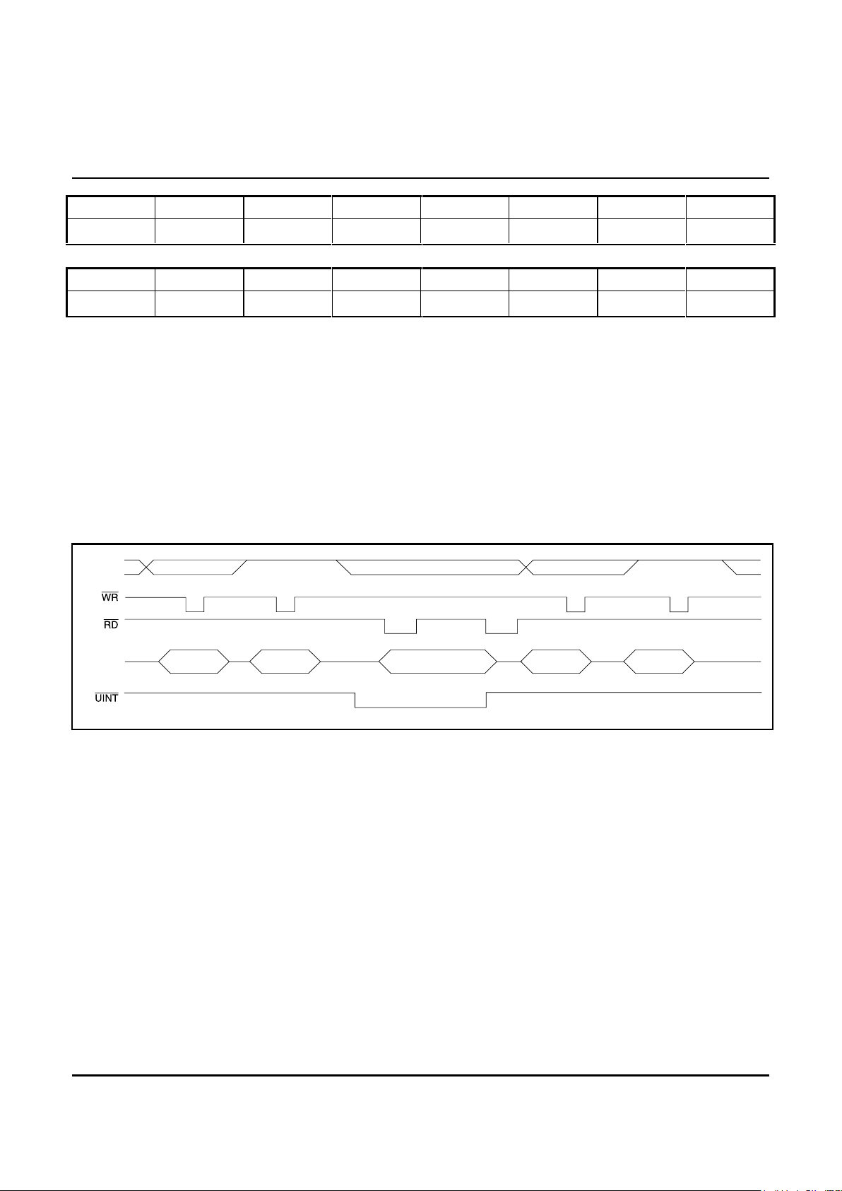
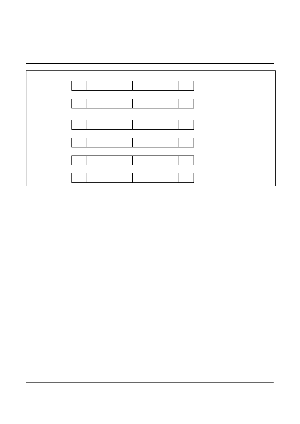
FIGURE 2: Interface Bus Activity for Configuration Register Access
MS Byte LS Byte MS ByteDSP Use LS Byte
UD[0-7]
UA1:0 10 11 11 XXXX 10
73M2921
Advanced Single
Chip Modem
Page 12 of 41 TDK Semiconductor February 99 Rev M
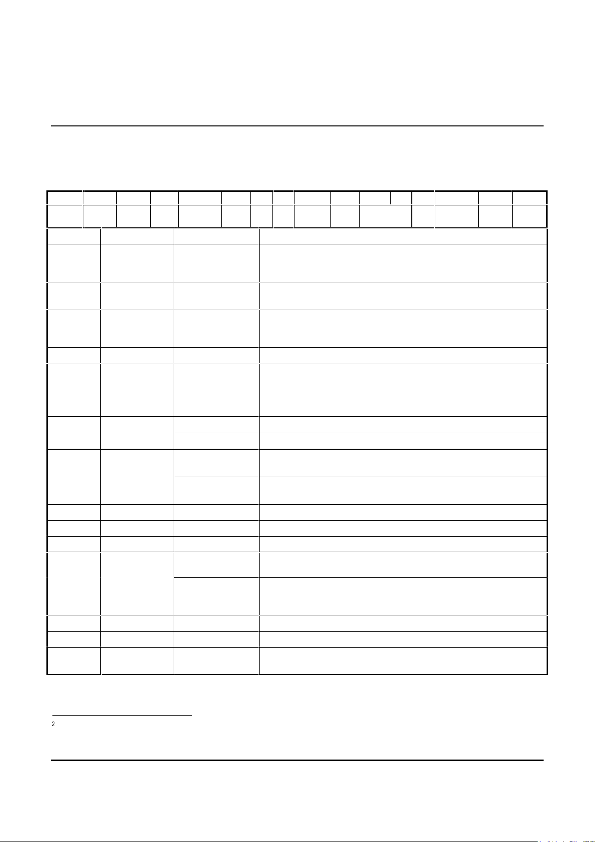
FIGURE 3: Write Command and Response
An example of a Configuration Register write cycle is shown in figures 2 and 3. Figure 2 shows the activity on the
interface register data pins and
8,17
. First there are two command bytes sent by the host processor. The
73M2921 responds (the contents of this response are not important to the host). Then the host writes the high
and low byte of the Configuration register to the 73M2921.
An example of the Control and Data bytes for a CRA write is shown in Figure 3. In this example we will write 90
00h to Configuration register one (CR1). This turns on the digital portion of the 73M2921.
The Control byte shows D6 set to indicate that a word size transfer will take place. D5 is zero to indicate a write
will occur. D4 is set to specify Configuration Register Access. D0 of the Control byte is always 1h for
Configuration Register Acc es s . The data byte sho ws D7 and D5 set to indic ate that CR1 is to be acc es sed. D4 is
always set for configuration register access. D3:0 are always zero for configuration register access.
The response from the 73M2921 will not be defined.
The word size transfer of CR1 data is also shown in figure 3. The MS byte is 90h. This enables the digital portion
of the 73M2921. The LS byte is 0h. Refer to the configuration register description on pages 10 and 11 for further
information.
01010001
10110000
XXXXXXXX
XXXXXXXX
MSB
Control Byte
Data Byte
COMMAND FROM HOST
DATA
RESPONSE FROM 73M2921
DATA
LSB
LSB
MSB
10010000
00000000
CR DATA FROM HOST
DATA
LSB
MSB
LOW BYTE
OF CR1
HIGH BYTE
OF CR1
CHOOSE
CR1
WRITE TO
CONFIGURA TION
REGISTERS
73M2921
Advanced Single
Chip Modem
February 99 Rev M TDK Semiconductor Page 13 of 41
REGISTER NAME: CR1 Configuration Register 1 ADDRESS: 05H (101b)
CR1 controls Diagnostic mo des, data wait, 5V power supp ly detect, speaker volume, ADC/DA C sampling rate,
slave sync, digit al loopback, digita l interface loop back, enable dig ital interface, an d enable timer . It also h as bits
that are reserved for test modes.
D15 D14 D13 D12 D11 D10 D9 D8 D7 D6 D5 D4 D3 D2 D1 D0
EN
TIMER
TEST3TEST2EN
DIGI
TDK TDK 0 0 SLAVE
SYNC16KHZ
SPKR VOL
(1:0)
05V
DETECT
DATA
WAIT
DIAG
MODE
BIT NO. NAME CONDITION DESCRIPTION
D0 Diagnostic
Mode
(Test Mode)
Always 0 DIAGNOSTIC MODE: Must be zero.
D1 Data Wait
(Test Mode)
Always 0 Must be zero.
D2 5V Detect
(output)
This is a logical 1 if the power supply to th e 73M2921 is in the
5V range. Note, this signal is valid only when EN ANALOG
(CR2: D10) is enabled.
D3 0 Not Used.
D4,D5 Speaker
Volume (1:0)
2
1 1
1 0
0 1
00
High Volume
Medium Volume
Low Volume
Speaker off
1 The ADC/DAC sampling rates are 16.0KHzD6 16KHz
0 The ADC/DAC sampling rates are 14.4KHZ (Default)
1
The phase error register measures the time between the rising
edge of RXC and the rising edge of TXC
D7
Slave Sync
(modem test
mode)
0 The phase error register measures the time between the rising
edge of EXC and the rising edge of TXC
D8,D9 0 Not Used
D10 TDK Always 0 TDK proprietary.
D11 TDK Always 0 TDK proprietary.
1
Enables the digital seri al inter f a ce. Pins TXC LK, RXC LK , TXD ,
and RXD are enabled. Must be set to one for normal operation.
D12
Enable Digital
Interface
0 Tri-states pins TXCLK and RXCLK (with a weak pull-down to 0).
RXD pin is driven to a 1, TXD is disabled at the input pin, and
the timer baud clocks are forced low.
D13 Test 2 0 Must be zero.
D14 Test 3 0 Must be zero.
D15 Enable Timer 1 When set to 1, sample, bit, and clocks for transmit and receive
are running. Baud (provided that EN DIGI is true).
9ROXPH3&0RXWSXWRQSLQ021XQGHUVRIWZDUHFRQWURO6HHDSSOLFDWLRQQRWHFRQFHUQLQJWKHXVHRIWKLVSLQ
 Loading...