

TDK Semiconductor Corporation 73M223-CP, 73M223-CL Datasheet
DESCRIPTION
73M223
1200 Baud FSK Modem
April 2000
FEATURES
The 73M223 modem device receives and transmits
serial and binary data over existing telephone
networks using Frequency Shift Keying (FSK). It
provides the filtering, modulation, and demodulation
to implement a serial, asynchronous data
communication channel. The 73M223 employs the
CCITT V.23 signaling frequencies of 1302 and 2097
Hz, operating at 1200 baud, and is intended for half
duplex operation over a two-line system.
The 73M223 provides a cost-effective alternative to
existing modem solutions. It is ideally suited for R.F.
data links, credit verification systems, point-of-sale
terminals, and remote process control.
CMOS technology ensures small size, low-power
consumption and enhanced reliability.
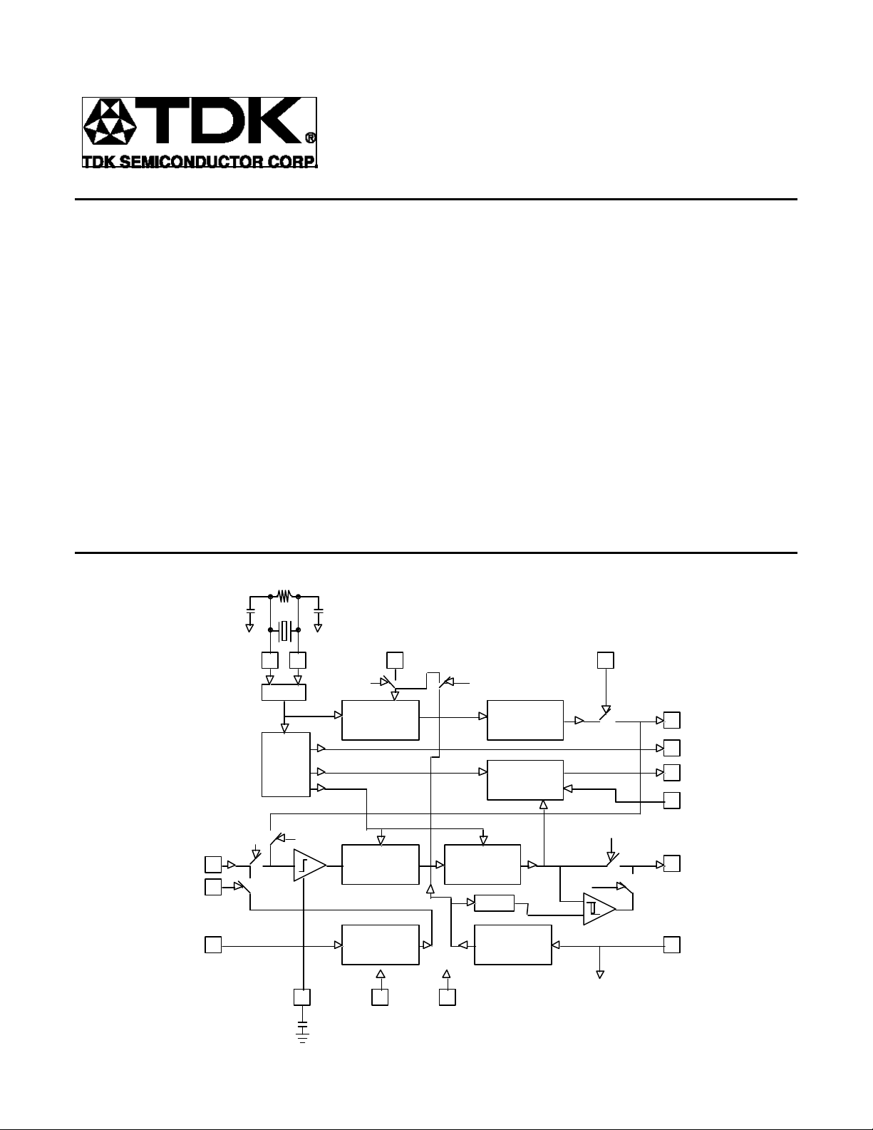
BLOCK DIAGRAM
TXD
OSC1 OSC2
13 14
OSC
DIGITAL
TIMING
SIGNALS
TEST
12
PROGRAMMABLE
DIGITAL
DIVIDER
• Low cost FSK Modem
• 1200 baud operation
• CMOS switched capacitor technology
• Built-in self-test feature
• On-chip filtering, and
Modulation/Demodulation
• Uses CCITT V.23 frequencies
• On chip crystal oscillator
• Low power/High reliability
• Does not require a microprocessor
• 10 mW @ 5 V supply
• 16-pin plastic packages
TX
7
TEST
PHASE
COHERENT
WAVE
SYNTHESIZER
SYNC
PHASE LOCKED
LOOP
16
TXA
15
CLK
915SYNC
SYN
RXA
FIL 5
RXF
2
4
TEST TEST
SLICER
3 CAP 1
DIGITAL
DEMODULATOR
SWITCHED CAP
BANDPASS
FILTER
VDD
VSS
TEST
DIGITAL
LP
FILTER
DELAY
RANDOM
SEQUENCE
GENERATOR
8
TEST
RXD
11
TEST6

73M223
1200 Baud FSK Modem
FUNCTIONAL DESCRIPTION
The 73M223 has four main functional sections:
timing, transmit, receive, and test. Each section of
the chip will be individually described below.
TIMING
The timing section contains the oscillator (OSC) and
logic, which generates digital timing signals used
throughout the chip. The time base can be derived
from 3.18 MHz crystal or an external digital input.
The digital timing logic divides the oscillator
frequency to give a 1200 Hz output than can be
used for system timing. The signaling frequencies
are 1302 Hz for logic “1” and 2097 Hz for logic “0.”
The modem will operate with clock inputs from 330
kHz to 7.0 MHz. However, the signaling frequencies
and the system timing will be directly proportional to
the difference in clock frequency.
TRANSMITTER
The 73M223 transmitter consists of a programmable
divider that drives a coherent phase frequency
synthesizer. The programmable divider is digitally
controlled via the Data Input pin (TXD). The output
of the divider clocks a 16 segment phase coherent
frequency synthesizer. A sine wave is constructed
by eight weighted capacitors which are the inputs to
a low pass filter. The synthesized signal is output
directly to the transmit pin TXA. The transmit signal
can be disabled by using the digital control pin TX.
The synchronization for sampling the digital output
at RXD is derived from a digital phase locked loop.
The phase locked loop is clocked at 16 times the bit
rate with a maximum lock period of 8 clocks to lock
on the data output signal. When SYN is low the
output of SYNC is nominally 1200 Hz, but is
resynchronized to the center of the data bit on each
data transition. When SYN is high, SYNC will output
a 1200 Hz clock, which is not synchronized to the
data on RXD.
SELF TEST MODE
The 73M223 features an autotest mode which
provides easy field test capability of the chip’s
functionality. The modem is placed in the test mode
by taking the test pin high. In the test mode the Data
Input pin is disconnected and the programmable
divider is driven by a pseudo random PN sequence
generator and the transmitter’s output is connected
to the receiver’s input. The input data to the
programmable divider is delayed by the system
delay time and compared to the digital output on
sync transitions. If the detected data matches the
delayed input data from the PN sequence counter,
the 73M223 is properly functioning as indicated by
RXD low. A high on the RXD pin indicates a
functional problem on the 73M223.
RECEIVER
The 73M223’s receiver comprises three sections:
the input bandpass filter, the synchronization loop,
and the demodulator.
The input bandpass filter is a four pole Butterworth
filter, implemented using switched capacitor
technology. This filter reduces wideband noise which
significantly improves data error rates. The 73M223
can be configured with the bandpass filter in series
with the receiver by setting FIL = 1 and inserting the
received signal at RXF (recommended
configuration). The bandpass filter can be deleted
from the system by setting FIL = 0 and inputting the
received signal through RXA.
The demodulator is used to detect a received mark
or space.
2
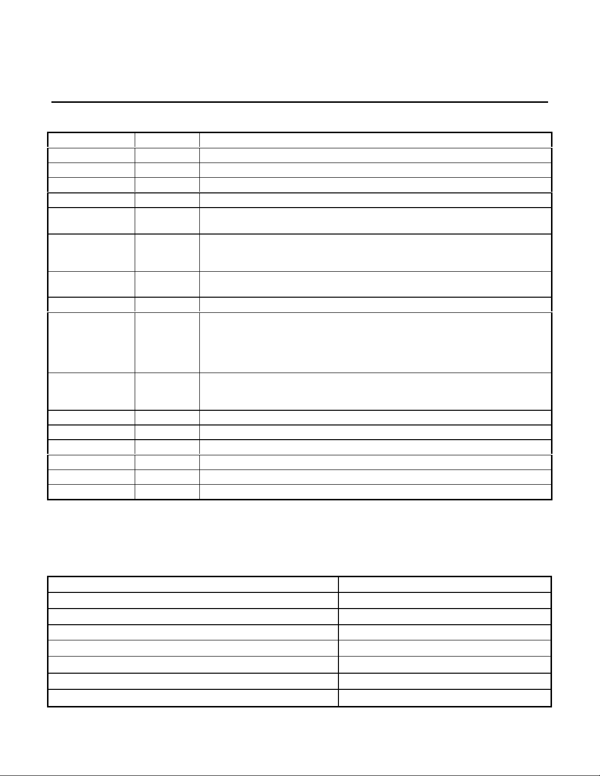
PIN DESCRIPTION
PIN NO. PIN NAME DESCRIPTION
1 VDD Positive Supply Voltage. Bypasses to Vss with 0.1 µF capacitor.
2 RXA Receive Analog Input. Analog input from the telephone network.
3 CAP Capacitor. Connect a 0.1µF capacitor between Pin 3 and ground (VSS).
4 RXF Filtered Receive Analog Input
5 FIL Analog Input Control. A logical 1 selects the filtered input. A logical 0 selects
the non-filtered input.
6 TEST Self-Test Mode Control. Normal operation when a logical 0.A logical 1 places
the device into the self-test mode. A low appears at RXD, to indicate a
properly functioning device.
7 TX Transmitter Control. A logical 0 selects transmit mode. A logical 1 selects a
stand-by condition forcing TXA to VDD/2 VDC.
8 VSS Ground
9 SYNC Synchronous Clock Output. Digital output synchronized with the 1200 bit/s
received data when SYN is low and used to sample the received data or eye
pattern. The falling edge of SYNC should be used to sample RXD. When SYN
is high a !@)) Hz clock is output. The standard data rate and clock are valid
only when the standard 3.1872 MHz crystal is used.
10 SYN Sync Enable. A logic 0 locks the SYNC clock PLL to the 1200 baud receive
data. A logic 1 disables the receive data PLL, and connects SYNC to the 1200
Hz reference.
11 RXD Receiver Digital Output
12 TXD Transmitter Digital Input
13 OSC1 Crystal Input (3.1872 MHz) or External Clock Input
14 OSC2 Crystal Return.
15 CLK 1200 Hz Square wave Output. Can drive up to 10 CMOS loads.
16 TXA Transmitter Analog Output.
73M223
1200 Baud FSK Modem
ELECTRICAL SPECIFICATIONS
Recommended conditions apply unless otherwise specified.
ABSOLUTE MAXIMUM RATINGS
Operation outside these rating limits may cause permanent damage to this device.
PARAMETER RATING
Power Supply Voltage (VDD-VSS) 7 V
Analog Input Voltage at RXA - 0.3 to VDD V
Analog Input Voltage at RXF - 3 to VDD V
Digital Input Voltage VSS – 0.3 to VDD + 0.3 V
Storage Temperature Range
Operating Temperature Range
Lead Temperature (10 secs soldering)
3
- 65 to + 150 °C
- 25 to + 70 °C
260 °C
 Loading...