

TDK Semiconductor Corporation 73K321L-IP, 73K321L-IH Datasheet
73K321L
CCITT V.23, V.21
Single-Chip Modem
April 2000
DESCRIPTION
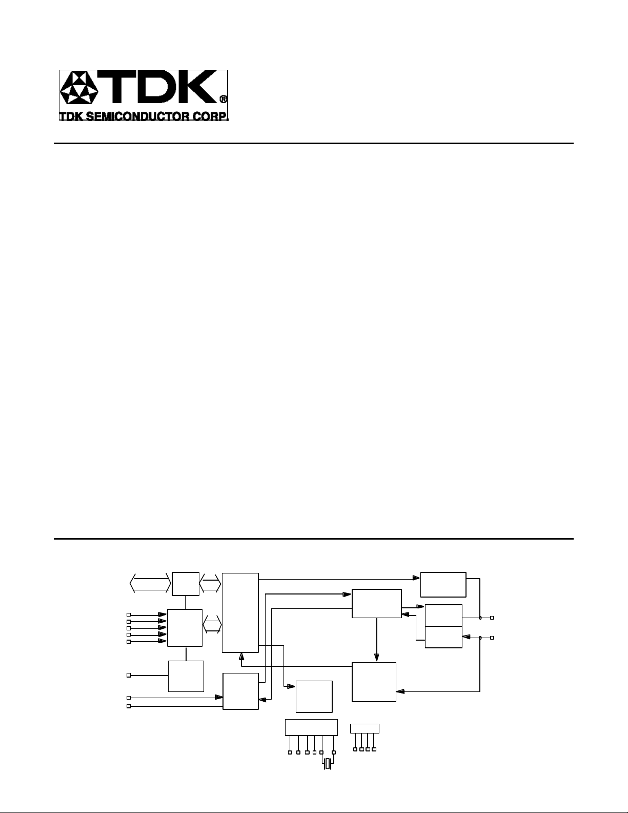
The 73K321L is a highly integrated single-chip
modem IC which provides the functions needed to
construct a CCITT V.23 and V.21 compatible
modem, capable of 0-300 bit/s full-duplex or 0-1200
bit/s half-duplex operation over dial-up telephone
lines. The 73K321L provides 1200 bit/s operation in
V.23 mode and 300 bit/s in V.21 mode. The
73K321L also can both detect and generate the
2100 Hz answer tone needed for call initiation. The
73K321L integrates analog, digital, and switchedcapacitor array functions on a single substrate,
offering excellent performance and a high level of
functional integration in a single 28-pin DIP or PLCC
package. The 73K321L operates from a single +5V
supply with very low power consumption.
The 73K321L includes the FSK
modulator/demodulator functions, call progress and
handshake tone monitor test modes, and a tone
generator capable of producing DTMF, answer,
calling tones. The 73K321L is designed to appear to
the systems designer as a microprocessor
peripheral, and will easily interface with popular onechip microprocessors (80C51 typical) for control of
modem functions through its 8-bit multiplexed
address/data bus or via an optional serial control
bus. An ALE control line simplifies address
demultiplexing. Data communications occurs
through a separate serial port only.
(continued)
FEATURES
• One-chip CCITT V.23 and V.21 standard
compatible modem data pump
• Full-duplex operation at 0-300 bit/s (V.21) or
0-1200 bit/s (V.23) forward channel with or
without 0-75 bits/s back channel
• Full Duplex 0-1200 bit/s (V.23) in 4-wire mode
• Pin and software compatible with other TDK
Semiconductor Corporation K-Series 1-chip
modems
• Interfaces directly with standard micro-
processors (8048, 80C51 typical)
• Serial port for data transfer
• Call progress, carrier, precise answer tone
(2100 Hz), calling tone (1300 Hz) and FSK
mark detectors
• DTMF generator
• Test modes available: ALB, DL, RDL, Mark,
Space, Alternating bit patterns
• Precise automatic gain control allows 45 dB
dynamic range
• CMOS technology for low power
consumption using 60 mW @ 5V from a
single power supply
AD0-AD7
RD
WR
ALE
CS
RESET
INT
TXD
RXD
DATA
BUS
BUFFER
READ
WRITE
CONTROL
LOGIC
STATUS
AND
CONTROL
LOGIC
8-BIT
BUS
FOR
CONTROL
AND
STATUS
SERIAL
PORT
FOR
DATA
BLOCK DIAGRAM
DEMODULATOR
TESTS:
ALB,DLB
RDLB
PATTERNS
CLOCK
GENERATOR
CLK
TXCLK
EXCLK
RXCLK
XTL1
POWER
XTL2
FSK
MODULATOR/
SMART
DIALING
&
DETECT
FUNCTIONS
ISET
VDD
GND
VREF
DTMF &
TONE
GENERATORS
TRANSMIT
FILTER
RECEIVE
FILTER
TXA
RXA

73K321L
CCITT V.23, V.21
Single-Chip
DESCRIPTION (continued)
The 73K321L is ideal for either free standing or
integral system modem applications where multistandard data communications over the 2-wire
switched telephone network is desired. Typical uses
include videotex terminals, low-cost integral modems
and built-in diagnostics for office automation or
industrial control systems. The 73K321L’s high
functionality, low power consumption and efficient
packaging simplify design requirements and increase
system reliability in these applications. A complete
modem requires only the addition of the phone line
interface, a control microprocessor, and RS-232 level
converter for a typical system. The 73K321L is part of
TDK Semiconductor's K-Series family of pin and
function compatible single-chip modem products.
These devices allow systems to be configured for
higher speeds and Bell or CCITT operation with only
a single component change.
OPERATION
FSK MODULATOR/DEMODULATOR
The FSK modulator produces a frequency
modulated analog output signal using two discrete
frequencies to represent the binary data. V.21 mode
uses 980 and 1180 Hz (originate, mark and space)
or 1650 and 1850 Hz (answer, mark and space).
V.23 mode uses 1300 and 2100 Hz for the main
channel and 390 and 450 Hz for the back channel.
The modulation rate of the back channel is up to 75
baud. Demodulation involves detecting the received
frequencies and decoding them into the appropriate
binary value.
PASSBAND FILTERS AND EQUALIZERS
High and low band filters are included to shape the
amplitude and phase response of the transmit and
receive signals and provide compromise delay
equalization and rejection of out-of-band signals in the
receive channel. Amplitude and phase equalization
are necessary to compensate for distortion of the
transmission line and to reduce intersymbol
interference in the bandlimited receive signal.
AGC
The automatic gain control maintains a signal level
at the input to the demodulators which is constant to
within 1 dB. It corrects quickly for increases in signal
which would cause clipping and provides a total
receiver dynamic range of >45 dB.
PARALLEL BUS INTERFACE
Four 8-bit registers are provided for control, option
select and status monitoring. These registers are
addressed with the AD0, AD1, and AD2 multiplexed
address lines (latched by ALE) and appear to a
control microprocessor as four consecutive memory
locations. Two control registers and the tone register
are read/write memory. The detect register is read
only and cannot be modified except by modem
response to monitored parameters.
SERIAL CONTROL INTERFACE
The Serial Command mode allows access to the
73K321L control and status registers via a serial
command port. In this mode the AD0, AD1 and AD2
lines provide register addresses for data passed
through the data pin under control of the RD and
WR lines. A read operation is initiated when the RD
line is taken low. The first bit is available after RD is
brought low and the next seven cycles of EXCLK will
then transfer out seven bits of the selected address
location LSB first. A write takes place by shifting in
eight bits of data LSB first for eight consecutive
cycles of EXCLK. WR is then pulsed low and data
transferred into the selected register occurs on the
rising edge of WR.
SPECIAL DETECT CIRCUITRY
The special detect circuitry monitors the received
analog signal to determine status or presence of
carrier, answer tone and weak received signal (long
loop condition). Special tones such as FSK marking
and the 1300 Hz calling tone are also detected. A
highly frequency selective call progress detector
provides adequate discrimination to accurately
detect European call progress signals.
DTMF GENERATOR
The DTMF generator will output one of 16 standard
tone-pairs determined by a 4-bit binary value and TX
DTMF mode bit previously loaded into the tone
register. Dialing is initiated when the DTMF mode is
selected using the tone register and the transmit
enable (CR0 bit D1) is changed from 0 to 1.
2
PIN DESCRIPTION
POWER
73K321L
CCITT V.23, V.21
Single-Chip Modem
NAME PLCC/DIP
PIN NUMBER
GND 28 I System Ground.
VDD 15 I Power supply input, 5V ±10%. Bypass with 0.1 and 22 µF capacitors
VREF 26 O An internally generated reference voltage. Bypass with 0.1 µF
ISET 24 I Chip current reference. Sets bias current for op-amps. The chip
PARALLEL MICROPROCESSOR CONTROL INTERFACE
ALE 12 I Address latch enable. The falling edge of ALE latches the address on
AD0-AD7 4-11 I/O Address/data bus. These bidirectional tri-state multi-plexed lines carry
CS 20 I Chip select. A low during the falling edge of ALE on this pin allows a
CLK 1 O Output clock. This pin is the output of the crystal oscillator frequency
INT 17 O Interrupt. This open drain output signal is used to inform the
RD 14 I Read. A low requests a read of the 73K321L internal registers. Data
RESET 25 I Reset. An active high signal high on this pin will put the chip into an
TYPE DESCRIPTION
to GND.
capacitor to GND.
current is set by connecting this pin to VDD through a 2 MΩ resistor.
ISET should be bypassed to GND with a 0.1µF capacitor.
AD0-AD2 and the chip select on CS .
information to and from the internal registers.
read cycle or a write cycle to occur. AD0-AD7 will not be driven and
no registers will be written if CS (latched) is not active. The state of
CS is latched on the falling edge of ALE.
only in the 73K321.
processor that a detect flag has occurred. The processor must then
read the detect register to determine which detect triggered the
interrupt. INT will stay low until the processor reads the detect register
or does a full reset.
cannot be output unless both RD and the latched CS are active or
low.
inactive state. All control register bits (CR0, CR1, Tone) will be reset.
The output of the CLK pin will be set to the crystal frequency. An
internal pull down resistor permits power on reset using a capacitor to
VDD.
3
73K321L
CCITT V.23, V.21
Single-Chip
PARALLEL MICROPROCESSOR CONTROL INTERFACE (continued)
NAME
WR 13 I
SERIAL MICROPROCESSOR CONTROL INTERFACE
AD0-AD2 4-6 I
DATA (AD7) 11 I/O
RD 14 I Read. A low on this input informs the 73K321L that data or status
WR 13 I Write. A low on this input informs the 73K321L that data or status
NOTE: The Serial Control mode is provided by tying ALE high and CS low. In this configuration AD7 becomes
DATA and AD0, AD1 and AD2 become the address only. See the Serial Control Timing diagrams on
page 18
PLCC/DIP
PIN NUMBER
TYPE DESCRIPTION
Write. A low on this informs the 73K321L that data is available on
AD0-AD7 for writing into an internal register. Data is latched on the
rising edge of WR. No data is written unless both WR and the latched
CS are low.
Register Address Selection. These lines carry register addresses and
should be valid during any read or write operation.
Serial Control Data. Data for a read/write operation is clocked in or
out on the falling edge of the EXCLK pin. The direction of data flow is
controlled by the RD pin. RD low outputs data. RD high inputs data.
information is being read by the processor. The falling edge of the
RD signal will initiate a read from the addressed register. The RD
signal must continue for eight falling edges of EXCLK in order to read
all eight bits of the referenced register. Read data is provided LSB
first. Data will not be output unless the RD signal is active.
information has been shifted in through the DATA pin and is available
for writing to an internal register. The normal procedure for a write is
to shift in data LSB first on the DATA pin for eight consecutive falling
edges of EXCLK and then to pulse WR low. Data is written on the
rising edge of WR.
4
DTE USER INTERFACE
73K321L
CCITT V.23, V.21
Single-Chip Modem
NAME
EXCLK 19 I
RXCLK 23 O
RXD 22
TXCLK 18 O Transmit Clock. TXCLK is always active. In V.23 mode the output is
TXD 21 I
ANALOG INTERFACE AND OSCILLATOR
RXA 27 I Received modulated analog signal input from the phone line.
TXA 16 O Transmit analog output to the phone line.
XTL1
XTL2
PLCC/DIP
PIN NUMBER
2
3
TYPE DESCRIPTION
External Clock. Used for serial control interface to clock control data
in or out of the 73K321L.
Receive Clock. A clock which is 16 x1200, or 16 x 75 in V.23 mode,
or 16 x 300 baud data rate is output in V.21.
O/
Weak
Pull-up
I
I
Received Digital Data Output. Serial receive data is available on this
pin. The data is always valid on the rising edge of RXCLK when in
Synchronous mode. RXD will output constant marks if no carrier is
detected.
either a 16 x 1200 baud clock or 16 x 75 baud, in V.21 mode the clock
is 16 x 300 baud.
Transmit Digital Data Input. Serial data for transmission is input on
this pin. In Asynchronous modes (1200 or 300 baud) no clocking is
necessary.
These pins are for the internal crystal oscillator requiring an 11.0592
MHz Parallel mode crystal and two load capacitors to Ground. XTL2
can also be driven from an external clock.
5

73K321L
CCITT V.23, V.21
Single-Chip
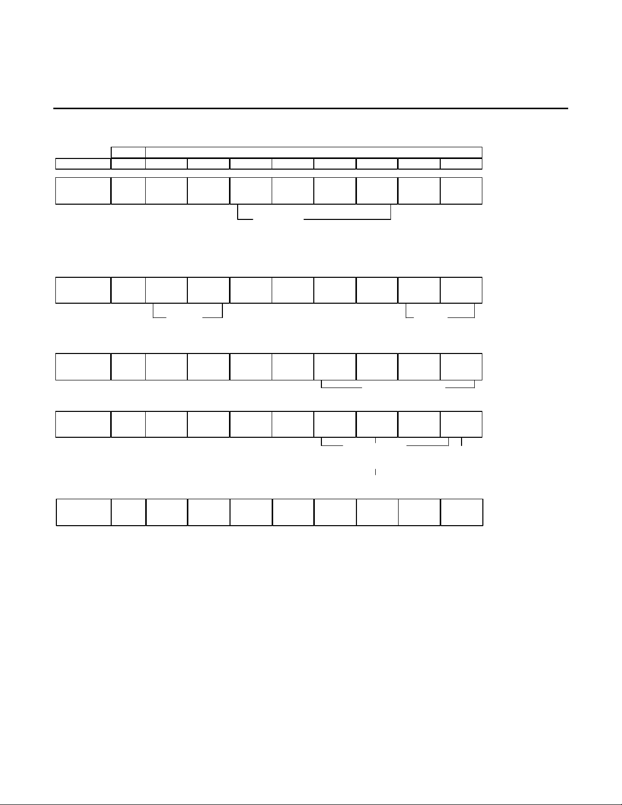
REGISTER DESCRIPTIONS
Four 8-bit internal registers are accessible for control
and status monitoring. The registers are accessed in
read or write operations by addressing the A0 and
A1 address lines in Serial mode, or the AD0 and
AD1 lines in Parallel mode. The AD0 and AD1 lines
are latched by ALE. Register CR0 controls the
method by which data is transferred over the phone
REGISTER BIT SUMMARY
ADDRESS
REGISTER
CONTROL
REGISTER
0
CONTROL
REGISTER
1
DETECT
REGISTER
TONE
CONTROL
REGISTER
ID
REGISTER
CR0
CR1
DR
TR
ID
AD2 - AD0
000
001
010
011
110
D7
TRANSMIT
MODE 4
TRANSMIT
PATTERN
1
X X X
RXD
OUTPUT
CONTROL
ID
D6 D5
0
TRANSMIT
PATTERN
0
TRANSMIT
CALLING
TONE
ID ID ID
TRANSMIT
ENABLE
DETECT
INTERRUPT
RECEIVE
TRANSMIT
ANSWER
MODE
3
DATA
TONE
line. CR1 controls the interface between the
microprocessor and the 73K321L internal state. DR
is a detect register which provides an indication of
Monitored modem status conditions. TR, the tone
control register, controls the DTMF generator;
answer and guard tones and RXD output gate used
in the modem initial connect sequence. All registers
are read/write except for DR which is read only.
Register control and status bits are identified below:
DATA BIT NUMBER
D4 D3 D2 D1 D0
TRANSMIT
MODE
2
ADD PH. EQ.
(V.23)
TRANSMIT
DTMF
TRANSMIT
MODE
1
CLK
CONTROL
CARRIER
DETECT
DTMF3 DTMF1
X X X X
TRANSMIT
MODE
0
RESET
SPECIAL
TONE
DTMF2/
V.23 FDX
TRANSMIT
ENABLE
TEST
MODE
1
CALL
PROGRESS
ANSWER/
ORIGINATE
TEST
MODE
0
LONG
LOOP
DTMF0/
ANSWER/SPEC.
TONE SELECT
NOTE: When a register containing reserved control
bits is written into, the reserved bits must be
programmed as 0's.
X = Undefined, mask in software
6
REGISTER ADDRESS TABLE
0=RECEIVE @ 1200 BIT/S, TRANSMIT @ 75 BIT/S
1=RECEIVE @ 75 BIT/S, TRANSMIT @ 1200 BIT/S
73K321L
CCITT V.23, V.21
Single-Chip Modem
CONTROL
REGISTER
0
CONTROL
REGISTER
1
DETECT
REGISTER
TONE
CONTROL
REGISTER
ID
REGISTER
ADDRESS
AD2 - AD0REGISTER
000
CR0
001
CR1
010
DR
011
TR
10 110 ID ID ID ID
D7 D6 D5 D4 D3 D2 D1 D0
TRANSMIT
MODE 4
0=V.23 FSK
1=V.21 FSK
TRANSMIT
PATTERN
1
00=TX DATA
01=TX ALTERNATE
10=TX MARK
11=TX SPACE
X X X
RXD
OUTPUT
CONTROL
RXD PIN
0=NORMAL
1=TRI STATE
0 0
TRANSMIT
PATTERN
0
TRANSMIT
CALLING
TONE
0=OFF
1=ON
TRANSMIT
MODE
3
0000=PWR DOWN
1100=FSK
0001=TRANSMIT DTMF, CALL PROGRESS DETECTION
ENABLE
DETECT
INTERRUPT
0=DISABLED
1=ENABLED
RECEIVE
DATA
OUTPUTS
RECEIVED
DATA STREAM
TRANSMIT
ANSWER
TONE
0=OFF
1=ON
0=NORMAL EQ.
1=ADD EXTRA
PHASE EQ.
IN V.23
DATA BIT NUMBER
TRANSMIT
MODE
2
ADD PH. EQ.
TRANSMIT
DTMF
0=DATA
1=TX DTMF
TRANSMIT
MODE
0
CLK
CONTROL
0=XTAL
1= NOT SUPPORTED IN THIS DEVICE
CARRIER
DETECT
DTMF3
X X X X
RESET
0=NORMAL
1=RESET
SPECIAL
TONE
0=CONDITION NOT DETECTED
1=CONDITION DETECTED
DTMF2/
V.23 FDX
4 BIT CODE FOR 1 OF 16
DUAL TONE COMBINATIONS. OVERIDES
OTHER TRANSMIT MODES
0=HALF DUPLEX V.23
1=ALLOWS V.23 FULL
DUPLEX OPERATION
TRANSMIT
ENABLE
0=DISABLE
TXA OUTPUT
1=ENABLE
TXA OUTPUT
TEST
MODE
1
00=NORMAL
01=ANALOG LOOPBACK
10=REMOTE DIGITAL
LOOPBACK
11=LOCAL DIGITAL
LOOPBACK
CALL
PROGRESS
DTMF1
ORIGINATE/
ANSWER
IN V.21 MODE:
0=ANSWER
1=ORIGINATE
IN V.23 MODE :
TEST
MODE
0
LONG
LOOP
DTMF0/
SPECIAL
TONE
0=ANSWER TONE FREQ.=2225 Hz
FSK MARK WILL BE INDICATED
BY SPECIAL TONE BIT IN DR
1=ANSWER TONE FREQ.=2100 Hz
EITHER 2100 Hz (IN ORIG.) OR
1300 Hz (IN ANS.) WILL BE
INDICATED BY SPECIAL TONE
BIT IN DR
00XX=73K212AL, 322L, 321L
01XX=73K221AL, 302L
10XX=73K222AL, 222BL
1100=73K224L
1110=73K324L
1100=73K224BL
1110=73K324BL
X = Undefined, mask in software
0 = Only write zero to these locations
7
73K321L
CCITT V.23, V.21
Single-Chip
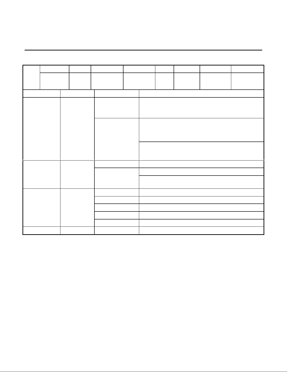
CONTROL REGISTER 0
D7 D6 D5 D4 D3 D2 D1 D0
CR0
000
BIT NO. NAME CONDITION DESCRIPTION
D0
TRANSMIT
MODE 4
0 TRANSMIT
Answer/
Originate
MODE 3
0
TRANSMIT
MODE 2
Selects Answer mode in V.21 (transmit in high band,
receive in low band) or in V.23 mode, receive at1200 bit/s
and transmit at 75 bit/s.
0 TX DTMF TRANSMIT
ENABLE
ANSWER/
ORIGINATE
1
D1
D7, D5, D4, D2 Transmit
D6, D3 Unused N/A Not used; must be written as “0”
Transmit
Enable
Mode
D7 D5 D4 D2
0 0 0 0 Power Down
0 0 0 1 Transmit DTMF
0 1 1 0 V.23 Mode
1 1 1 0 V.21 Mode
0 Disables transmit output at TXA.
1
Selects Originate mode in V.21 (transmit in low band,
receive in high band) or in V.23 mode, receive at 75 bit/s
and transmit at 1200 bit/s. If in V.23 and D2 of TR=1,
selects V.23 full duplex operation in 4-wire configuration.
Note: This bit works with TR bit D0 to program special
tones detected in Tone Register. See detect and tone
registers.
Enables transmit output at TXA.
Note: Answer tone and DTMF TX control require TX
enable.
8
 Loading...