

Page 1

CPFE500F Application Note Document Number : 61066 iss 2 Page 1 of 17
CPFE500
AC/DC Power Supply Series
APPLICATION NOTE
Page 2

CPFE500F Application Note Document Number : 61066 iss 2 Page 2 of 17
INDEX
1. INPUT..................................................................................................................................................................3
AC INPUT LINE REQUIREMENTS ..................................................................................................................... 3
2. DC OUTPUT .......................................................................................................................................................3
OUTPUT VOLTAGES .........................................................................................................................................3
REMOTE SENSE ................................................................................................................................................ 3
OUTPUT OR-ING DIODE ...................................................................................................................................3
OUTPUT VOLTAGE TRIM .................................................................................................................................. 4
OUTPUT GOOD LED .......................................................................................................................................... 5
EFFICIENCY .......................................................................................................................................................5
CAPACITIVE LOAD OPERATION ......................................................................................................................5
SERIES CONNECTION ......................................................................................................................................5
PARALLEL CONNECTION .................................................................................................................................5
3. OUTPUT CHARACTERISTICS ..........................................................................................................................7
RIPPLE / NOISE.................................................................................................................................................. 7
POWER SUPPLY TIMING ..................................................................................................................................8
4. CONTROL SIGNALS .......................................................................................................................................... 8
AUXILIARY SUPPLY (AUX) ................................................................................................................................ 9
POWER ON SIGNAL (ENA)................................................................................................................................ 9
INVERTER OUTPUT GOOD (IOG)..................................................................................................................... 9
REMOTE ON/OFF............................................................................................................................................... 9
5. OUTPUT PROTECTION ................................................................................................................................... 11
NO LOAD OPERATION ....................................................................................................................................11
OVER CURRENT OPERATION (OCP) ............................................................................................................11
OVER TEMPERATURE PROTECTION (OTP)................................................................................................. 11
OVER VOLTAGE PROTECTION (OVP)........................................................................................................... 11
6. COOLING REQUIREMENTS............................................................................................................................ 12
7. PSU MOUNTING........................................................................................................................................... 13
8. RELIABILITY .....................................................................................................................................................14
9. ELECTROMAGNETIC COMPATIBILITY.......................................................................................................... 15
INSTALLATION GUIDELINES FOR EMC ........................................................................................................ 16
10. CONNECTION ................................................................................................................................................ 17
AC INPUT CONNECTOR (J1) MATING PARTS ..............................................................................................17
AC INPUT CONNECTOR (J1) PIN DEFINITION..............................................................................................17
SIGNAL CONNECTORS (J2,J3) MATING PARTS........................................................................................... 17
SIGNAL CONNECTORS (J2,J3) PIN DEFINITION ..........................................................................................17
POWER TERMINALS .......................................................................................................................................17
11. WEIGHTS........................................................................................................................................................17
12. TEST RESULTS .............................................................................................................................................17
Page 3

CPFE500F Application Note Document Number : 61066 iss 2 Page 3 of 17
1. INPUT
AC INPUT LINE REQUIREMENTS
See datasheet for specification of input line requirements (including Input voltage range, Input frequency, Input
harmonics, Input current and leakage current)
The power supply will automatically recover from AC power loss and shall be capable of start-up under peak
loading at 85VAC.
Repetitive ON/OFF cycling of the AC input voltage shall not damage the power supply or cause the input fuse to
blow.
• Input Fuse
Not user serviceable. Fast Acting, high breaking capacity, ceramic fuse, 15A/250V rated
• Input undervoltage
The power supply is not designed to be protected against the permanent application of an input voltage
below the minimum specified. Avoid or protect against input undervoltage conditions that exceed 30seconds
duration.
2. DC OUTPUT
OUTPUT VOLTAGES
Output voltages are factory set at 12V, 24V, 28V or 48V +/-2% depending on the model.
The output voltage may be subsequently adjusted using the potentiometer ‘R3’ within the ranges listed below :-
12V model 9.6V ~ 14.4V
24V model 22.4V ~ 33.6V
28V model 22.4V ~ 33.6V
48V model 38.4V ~ 57.6V
On models fitted with output OR-ing diode, the maximum voltage shown above will be the voltage before the
OR-ing diode. The maximum adjustment voltage after the OR-ing diode will subsequently be reduced by up to
1V.
The main output voltage, auxiliary output voltage and output signals are isolated from the baseplate but not
isolated from each other. The remote on/off control is isolated from all outputs and baseplate.
REMOTE SENSE
Remote sensing, if required, can be connnected via the control signal connectors J2,J3 (pins 1 & 2) and
compensates for both +Ve and –Ve power line voltage drop. The remote sense terminals are internally
connected to +ve and -ve outputs via 100R/0.25W resistors and maybe left unconnected if not required. On
models fitted with output OR-ing diode, the internal connection is before the diode.
When using remote sense, the maximum power cable voltage drop should be limited to :-
+Ve Power cable 1.5V max (includes OR-ing diode drop on models fitted with OR-ing diode)
-Ve Power cable 0.5V max
OUTPUT OR-ING DIODE
CPFE500 series PSU maybe specified with or without integral OR-ing diode.
For models with OR-ing diode, the diode is fitted in the +ve output terminal of the PSU.
On 12V,24V & 28V models, the OR-ing diode is a schottky type rectifier.
On 48V models, the OR-ing diode is an ultrafast type standard rectifier.
Page 4

CPFE500F Application Note Document Number : 61066 iss 2 Page 4 of 17
OUTPUT VOLTAGE TRIM
Output voltage can be adjusted within the normal range by connecting a resistance or applying external voltage
to the TRIM terminal (J2,J3 pin 8)
Take care not to exceed the normal voltage adjustment range as Overvoltage protection (OVP) may activate
and shutdown the PSU.
When increasing or decreasing the output voltage, observe the PSU maximum output power and current.
If required, remote sense can be used in conjunction with the output voltage trim function.
Internally, the TRIM terminal is connected to the voltage reference of the output voltage control amplifier – see
figure 1 below :-
Figure 1 – CPFE500 TRIM terminal Internal Circuit
The output voltage can be decreased from the adjusted set-point by connecting an external resistance between
TRIM and –S.
Do not connect external resistance between TRIM and +S, this will cause output instability.
Alternatively the trim terminal maybe driven by an external voltage, see figure 2 below.
Typically when left unconnected, the TRIM terminal voltage is 0.75V.
When applying an external voltage to the TRIM terminal, the main output voltage follows the formula :-
VOUT = VOUT
NOM
x (V
TRIM
/ 0.75) (where VOUT
NOM
is the output voltage setting with
TRIM terminal unconnected)
Figure 2 – Adjusting the output voltage using an external voltage source
Page 5

CPFE500F Application Note Document Number : 61066 iss 2 Page 5 of 17
OUTPUT GOOD LED
A green LED adjacent to the output terminals provides a visual indication that output voltage is present.
The LED typically lights at the following output voltages :-
12V model 9V nom
24V model 19V nom
28V model 19V nom
48V model 31V nom
EFFICIENCY
A typical efficiency curve for a 12V model with OR-ing diode is shown below. This is the least efficient model.
24V, 28V & 48V models have typically 1~2% higher efficiency.
Models without OR-ing diode are additionally 1~2% more efficient.
The majority of dissipated heat is conducted into the baseplate, for the model shown, this dissipated heat is
~135Watts at full load / 115Vac dropping to ~110Watts at full load / 230Vac.
CAPACITIVE LOAD OPERATION
CPFE500 series has been tested with the following capacitive loads :-
12V model 42,000uF
24V model 18,000uF
28V model 18,000uF
48V model 10,500uF
Larger capacitive loads should be evaluated as required in the end application.
SERIES CONNECTION
It is possible to connect two CPFE500 psu outputs in series to provide higher voltage or split rail outputs.
Note that SELV outputs connected in series may create a non-SELV output.
PARALLEL CONNECTION
Parallel operation can be used to provide increased load current or achieve N+1 PSU redundant operation.
By connecting the PC terminal (J2,J3 pin 7) of each PSU together and setting the output voltages within +/-1%
the individual PSU’s will share the load current.
A maximum of 6 PSU’s of the same model can be connected in parallel.
Current balancing between units will have a some error and the maximum output current should be derated as
follows :-
2~3 units in parallel 90% of nominal output current
4~6 units in parallel 85% of nominal output current
Load current exceeding the limits above could result in operation of a PSU above it’s rated output capability.
Figures 3,4,5 below show typical wiring details for parallel connection of two CPFE500 psu’s.
For N+1 redundancy, specify CPFE models with integral output OR-ing diode, or alternatively fit an external ORing diode in the +ve output terminal of each PSU.
It is recommended to connect the –S voltage sense terminals of each PSU to a common load termination to
achieve the best balance of current between PSU’s.
The +S voltage sense terminal is optionally connected to the load to compensate for voltage drop in the +ve
power cable.
For N+1 redundant systems avoid connecting +S to the load as this creates a single fault condition for both
PSU’s.
Do not connect Trim terminals of PSU’s directly together. When using external voltage source at the Trim
terminal for paralleled PSU’s, insert a 10Kohm resistor in series with the voltage source for each PSU (see
Page 6

CPFE500F Application Note Document Number : 61066 iss 2 Page 6 of 17
Figure 5). Additional voltage drop across this 10Kohm series resistor will change the voltage programming
calculation – refer to Figure 1. For N+1 redundant systems, individual voltage source circuits would be advisable
for each PSU to maintain the system redundancy.
Figure 3 – Basic Parallel connection Figure 4 – Parallel connection with adjusted output
Figure 5 – Parallel connection with adjusted output from voltage source
Page 7

CPFE500F Application Note Document Number : 61066 iss 2 Page 7 of 17
3. OUTPUT CHARACTERISTICS
RIPPLE / NOISE
Ripple and noise is defined as periodic or random signals over a frequency range of 10Hz to 20MHz.
Measurements are to be made with an 20MHz bandwidth oscilloscope. Measurements are taken at the end of a
150mm length of a twisted pair of cables, terminated with a 100nF ceramic capacitor and a 120µF electrolytic
capacitor (see Figure 6). The earth wire of the oscilloscope probe should be as short as possible, winding a link
wire around the earth collar of the probe is the preferred method.
PSU
AC Input
Live
Neutral
Load
C1
C2
C1 = 120µF Electrolytic
C2 = 100nF Ceramic
Scope
Scope probe
earth collar
Scope
probe tip
15cm twisted
pair cable
Figure 6 – Ripple and Noise measurement method
Page 8

CPFE500F Application Note Document Number : 61066 iss 2 Page 8 of 17
POWER SUPPLY TIMING
Figure 7 – Timing Diagram
4. CONTROL SIGNALS
Control signals are available on two 10-way 2.5mm pitch header connectors (Molex 22-04-1101).
The pin functions of each connector are identical, see Figure 8 below :-
Figure 8 – Connector J2,J3 Pinout
J2,J3 Pin Function
1 +VE REMOTE SENSE
2 -VE REMOTE SENSE
3 COM
4 REMOTE ON/OFF -VE
5 REMOTE ON/OFF +VE
6 AUX
7 CURRENT SHARE
8 TRIM
9 ENA (Output Good)
10 IOG
Recommended mating parts are :Molex 22-01-1102 (Molex 5051 series 10way housing)
Molex 08-70-0064 (Molex 5159 series 22~28AWG crimp terminal)
Page 9

CPFE500F Application Note Document Number : 61066 iss 2 Page 9 of 17
AUXILIARY SUPPLY (AUX)
AUX is a 19~14VDC output for external circuits that is not affected by the remote on/off control.
Ground for AUX output is the COM terminal which is internally connected to –ve sense terminal.
Maximum load current for AUX output is 20mA. Avoid overload or short circuit of the AUX terminal as this may
cause internal damage to the PSU.
POWER ON SIGNAL (ENA)
The ENA signal is an open collector output which indicates that the output voltage is above a fixed threshold
level. The signal becomes low when the main output voltage exceeds the fixed threshold. The signal has
hysteresis on rising and falling voltage thresholds.
Ground for ENA signal is the COM terminal
Rising output voltage threshold for ENA low :-
12V model 8V typ
24V model 19V typ
28V model 19V typ
48V model 33V typ
Falling output voltage threshold for ENA high :-
12V model 6V typ
24V model 15V typ
28V model 15V typ
48V model 28V typ
The specifications for the ENA signal are :-
Signal Type Open collector referenced to COM terminal
Sink Current 10mA max
Open circuit voltage 75V max
INVERTER OUTPUT GOOD (IOG)
The IOG signal is an open collector output which provides an indication that the switching inverter is operating.
The signal is low when the inverter is normally operating and high when the inverter stops or is operating
abnormally. Ground for IOG signal is the COM terminal.
Note that the IOG signal may also become high/unstable for the following conditions :-
• Operation of output over current protection (OCP)
• Light load conditions with parallel operation
• Dynamic load conditions
The specifications for the IOG signal are :-
Signal Type Open collector referenced to COM terminal
Sink Current 5mA max
Open circuit voltage 35V max
REMOTE ON/OFF
The on/off control signal is isolated from input, output and other control signals by an optocoupler.
The voltage between on/off control terminals and other outputs/control lines should not exceed 60VDC.
Where higher isolation voltage is required, an external optocoupler should be employed – see Figure 12.
The PSU output is enabled when a voltage is applied to the on/off control terminals.
Page 10

CPFE500F Application Note Document Number : 61066 iss 2 Page 10 of 17
Internally, the remote on/off terminals are connected to an optocoupler LED via a 4K7 series resistor – see
Figure 9.
Figure 9 – Remote on/off control internal circuit
The on/off control is designed to be operated directly from the 12V Auxiliary supply.
When connecting to higher voltages, fit an external series resistor to limit the current as follows :-
ON/OFF Terminal current Output Voltage
2.5mA (+/-0.5mA) ON
Less than 0.15mA OFF
Figure 10 – on/off control with external switch Figure 11 – connection when on/off control is not used
Figure 12 – on/off control with external optocoupler
When on/off control is not required, the PSU may be permanently enabled as per figure 11 by fitting two
shorting links (supplied) to either connector J2 or J3. One link should be fitted between pins 3 & 4 and the
second link between pins 5 & 6 – see figure 13 below.
Page 11

CPFE500F Application Note Document Number : 61066 iss 2 Page 11 of 17
Figure 13 – Method to permanently enable the PSU
5. OUTPUT PROTECTION
NO LOAD OPERATION
There is no minimum load required for correct output voltage regulation.
OVER CURRENT OPERATION (OCP)
The PSU has constant current limiting with automatic recovery.
The OCP threshold is fixed and cannot be adjusted.
Note that continuous short circuit or overload for more than 30seconds might result in damage to the PSU.
OVER TEMPERATURE PROTECTION (OTP)
The PSU may activate over temperature protection if the cooling baseplate exceeds 90~115DegC for 12V
models or 105~130DegC for all other models. OTP will shutdown the main output. The Auxiliary output is not
affected during OTP condition.
To restart the PSU main output, allow the unit to cool and either :(i) remove the ac supply for 10 seconds and then reapply, or
(ii) cycle the on/off control
OVER VOLTAGE PROTECTION (OVP)
An overvoltage on the main output will cause the main output to shutdown. The Auxiliary output is not
affected during OVP condition.
To restart the PSU main output, either :(i) remove the ac supply for 10 seconds and then reapply, or
(ii) cycle the on/off control
Overvoltage threshold will vary according to PSU model as follows :-
Model OVP threshold range
12V model 15.0V ~ 17.4V
24V model 35.0V ~ 40.6V
28V model 35.0V ~ 40.6V
48V model 60.0V ~ 69.6V
Page 12

CPFE500F Application Note Document Number : 61066 iss 2 Page 12 of 17
6. COOLING REQUIREMENTS
CPFE500F is designed to mounted in any orientation except horizontal with baseplate uppermost.
The PSU requires a combination of conduction cooling for the baseplate and convection cooling for the PCB
mounted components.
The PSU maybe specified with or without factory fitted cover.
Convection cooling is best achieved with the PSU mounted in a vertical plane allowing convected air to flow
through the cover side or end ventilation slots and across the PCB mounted components.
If horizontal mounting is necessary, the PSU should be specified without cover wherever possible to achieve
best convection cooling and life expectancy for the PCB mounted components.
Where it is necessary to verify the PSU component temperatures in the end application, refer to Figure 14 for
internal component temperature limits.
Figure 14 – Internal Component Temperature Limits
Component Reference Component Function Temperature Limit
C1, C2, C3, C4, C5 EMC capacitor - Type X2 100DegC
C7, C8, C10, C14, C15 EMC capacitor - Type Y2 100DegC
R2, R9, R10 Surge Suppression Varistor 85DegC
L1, L2, L6 EMC filter chokes 130DegC
C11, C12, C25, C26 Bulk storage capacitor 67.5DegC *1
C16, C17, C22, C23 Output filtering capacitor 81DegC *1
Baseplate PSU baseplate 85DegC
Notes
*1 Temperature limits for electrolyti c capacitors C11,C12,C25,C26,C16,C17,C22,C23 are calculated to provide a 3year life expectancy.
Temperatures above the limit specified can be used up to a a maximum of 105DegC with a corresponding reduction in life expecta ncy.
The capacitor life expectancy will be halved for every 10DegC above the limit specified.
Page 13
CPFE500F Application Note Document Number : 61066 iss 2 Page 13 of 17
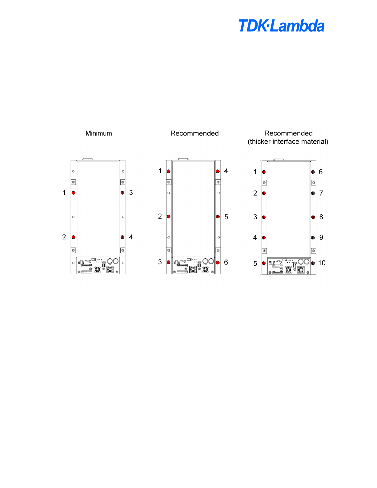
7. PSU MOUNTING
The PSU baseplate flatness is specified to be within 0.2mm across the width or length. A thermal interface
material should be used between the baseplate and system heatsink. The thickness of this material will
depend on the relative flatness of the two surfaces and should be chosen to provide thermal contact across
the whole area of the PSU baseplate.
The PSU has 10-off 4.5mm mounting holes in the baseplate (5-off on each side).
Use a mounting pattern to spread the force evenly over the baseplate. For thicker thermal interface
materials, use more fixings and tighten progressively .
See Figure 15 below for recommended mounting screw patterns.
Figure 15 – PSU Mounting
Page 14

CPFE500F Application Note Document Number : 61066 iss 2 Page 14 of 17
8. RELIABILITY
Calculating Model
Telcordia issue 1
Caluclation Method
Method 1 case 3
Environment
GB, GC - ground Benign, Controlled
Power
504w
Duty Cycle
100%
Baseplate
MTBF
MTBF
temperature °c
(hours)
(million hours)
25 887826 0.888
40 533421 0.533
80 115896 0.116
MTBF CPFE500F
0.100
1.000
25 35 45 55 65 75
Base Plate tem perature °c
MTBF (Million Hour s)
Page 15

CPFE500F Application Note Document Number : 61066 iss 2 Page 15 of 17
9. ELECTROMAGNETIC COMPATIBILITY
Figure 16 – Typical conducted EMC measurement (12V model, 230Vac 100% load)
Figure 17 – Typical conducted EMC measurement (24V model, 230Vac 100% load)
Figure 18 – Typical conducted EMC measurement (48V model, 230Vac 100% load)
Page 16

CPFE500F Application Note Document Number : 61066 iss 2 Page 16 of 17
L
N
CPFE500F
AC inlet
INSTALLATION GUIDELINES FOR EMC
Mounting
Good EMC performance comes through careful consideration of the power supply installation. All equipment
should be mounted inside an earthed metal box, with joints sealed with EMC gasket material where possible.
If this is not possible then use an earthed metal plane to mount the power supply and load.
Earth Starpoint
The earth connection from the AC supply should be routed to a chassis mounted ‘star-point’, located as close as
possible to the AC inlet. Note: Compliance with EN60950-1 practice requires the main protective earth
termination to have its own dedicated spring, washer and nut. The PSU earth and all other earth circuits should
be routed directly to the ‘star-point’, thereby reducing the possibility of creating earth loops in the system.
De-coupling
A significant Radiated and Conducted EMC performance can be achieved through the inclusion of de-coupling
‘Y’ capacitors, with a minimum value of 470pF, placed immediately adjacent to the AC inlet, as shown in figure
19.
Similar performance improvements can be
achieved through the use of a Schaffner IEC inlet
type FN 9222, which has these capacitors built in,
or the inclusion of a proprietary mains input filter.
TDK Lambda has a wide range of suitable mains
filters available for all circumstances.
Figure 19
Always de-couple the load using approximately 10 – 1000µF of capacitance per Amp of running current. Fit the
capacitance as close as possible to the load.
Cables
All cables and PCB tracks should be regarded as both radiation sources and receivers. The following tips will
assist in maximising EMC performance:
• Both AC input and DC power output cables should be run as close as possible to the earthed metal
box/plane.
• Input and output cables should be routed as far away from each other as possible, kept as short as
possible and, ideally, screened from each other.
• Tightly twist the AC input cables together. The DC power output cables should also be tightly twisted
together.
• If Remote Sense is used, also twist these wires tightly together and try to avoid running power and
sense cables together in the same loom.
• Loops in cables and PCB tracks should be eliminated or kept as small as possible.
Connecting between boxes
If cables must be connected between equipment boxes then at the closest possible point to the port where the
cables exit the 1st enclosure connect 100nF decoupling Y caps (between the output and earth). Note that these
capacitors must be rated at the working voltage. Ideally these capacitors should be between all signal cables
which have to connect between boxes although this may not be practical if fast switching [digital] signals are
involved (if this is the case then smaller value Y capacitors should be used).
ESD Protection
Where signal or control ports are connected to a user accessible panel (for example PSU inhibit to a switch,
module good to an indicator circuit, etc), these ports must be protected from electrostatic discharges. This can
be achieved by selecting suitable panel controls or by fitting ESD suppression devices to the connections on the
panel.
Page 17

CPFE500F Application Note Document Number : 61066 iss 2 Page 17 of 17
Conducted Immunity Protection
For conducted immunity protection of the option connector it is recommended to connect a capacitor (min 100n,
500v) between Aux common (pin3) and earth.
10. CONNECTION
AC INPUT CONNECTOR (J1) MATING PARTS
Tyco part
number
Description
350766-1 Tyco mate-N-lok 3-way housing UL94V-0
926893-1 Tyco female crimp 14~20AWG
926895-1 Tyco female crimp 18~24AWG
AC INPUT CONNECTOR (J1) PIN DEFINITION
Pin Function
J1-3 Live
J1-2 Earth - chassis
J1-1 Neutral
SIGNAL CONNECTORS (J2,J3) MATING PARTS
Molex part
number
Description
22-01-1102 Molex 5051 series 10-way housing UL94V-0
08-70-0064 Molex 5159 series crimp terminal 22~28AWG
SIGNAL CONNECTORS (J2,J3) PIN DEFINITION
J2, J3 pin Function
1 + sense
2 - sense
3 COM (return for pins 6,7,8,9,10)
4 - remote on/off
5 + remote on/off
6 Aux
7 Current share
8 Trim
9 ENA
10 IOG
POWER TERMINALS
The +ve and –ve output power terminals each have one M6x18 vertical stud.
M6 nuts, flat washers and spring washers are supplied fitted to each terminal.
Maximum recommended torque for the M6 terminals is 10Nm.
11. WEIGHTS
All models without cover = 1200g nominal
All models with cover = 1375g nominal
12. TEST RESULTS
Production test results are available online from: - http://testcert.emea.tdk-lambda.com/
The serial number and product code of the unit will need to be entered to retrieve test results from the online
database.
Test results are not packaged with the unit.
 Loading...