

Page 1

CM4 App Note 260424 issue 2.1.docx Document No.260424 Page 1 of 29
CM4
AC/DC Modular Power Supply Series
APPLICATION NOTES
Page 2

CM4 App Note 260424 issue 2.1.docx Document No. 260424 Page 2 of 29
Contents
Contents 2
1. Theory of Operation 3
2. Input Module Operation 4
3. Input Module Protection 5
4. Efficiency Performance 6
5. Power Ratings 7
6. System Cooling 8
7. Signalling 11
8. Output Module Operation 13
9. Advanced Output Module Features 16
10. Series Connected Outputs 20
11. Parallel Connected Outputs 21
12. Mechanical Dimensions and Mounting 24
13. Connector details 25
14. EMC Compliance 26
15. Reliability 27
16. Output Modules 28
17. Accessories 29
Page 3

CM4 App Note 260424 issue 2.1.docx Document No. 260424 Page 3 of 29
1. Theory of Operation
The diagram below outlines the topology and major internal components of a fully assembled CM4 configurable power supply. Four output slots
are provided and can be populated by any combination of output modules. The remaining components in the block diagram are housed in the
input and transformer modules.
The input module is responsible for receiving the AC mains line voltage and converting it to an appropriate DC voltage whilst providing protection
from AC line disturbances and preventing excessive EMI emissions and current harmonics. The integrated EMI filter attenuates high frequency
current emissions to levels below EN55032 class B. It also provides dual pole fusing, one fuse in each conductor and protection from line
disturbances as outlined in EN61000.
Inrush current is controlled by a resistive element upon initial connection to the AC line. Once the internal capacitances have been charged, the
resistive element is bypassed to reduce losses.
Active Power Factor Correction (PFC) is used to ensure an accurate input current waveform with extremely low harmonic content, exceeding the
requirements of EN61000. This stage also provides active input current limiting which prevents overloading of the input stage while maintaining
high power factor.
The output of the PFC stage charges the hold-up electrolytic capacitors which store enough energy to allow the CM4 configured product to
continue operating during minor line disturbances. Long lifetime and high temperature capacitors are used which ensures extended lifetime and
product reliability.
A highly efficient zero voltage switching circuit is used to drive the isolated transformer from the hold-up capacitors. The output modules connect
to the transformer secondary and provide safe isolated power to a high performance synchronous rectifier power converter. This power converter
is controlled using the latest analog control technology to produce superior output performance in a miniature size.
Page 4

CM4 App Note 260424 issue 2.1.docx Document No. 260424 Page 4 of 29
2. Input Module Operation
Startup & Shut Down
The CM input module operates from a universal input voltage range and starts automatically upon application of adequate AC mains voltage
(>84Vrms). After a short delay, the global 5V bias supply starts and the ACOK signal goes high to indicate that the mains voltage is present and
input stage is operating correctly. Once the ACOK signal is high, the output modules turn on and deliver power to the application loads. The
power good signals will indicate that the output voltages are within specification. The diagram below shows the normal start up/shut down
sequence and gives typical timings.
Typical timing values: t
1
≤2000 ms, t2 ≤400 ms, t3 ≤600 ms, t4 ≥15 ms, t5 ≥5ms (minimum), t6 ≥100 ms
When the AC mains voltage is removed, the internal hold-up capacitors will supply power to the load for typically 20 ms (t4+t5) at maximum
power. The ACOK signal will go low at least 5 ms before the output voltages fall below the power good threshold level. This allows the application
to prepare for the impending loss of power. The 5V bias supply will remain on for typically 100 ms, after the output modules have turned off.
Standby control
The unit may be completely shut down by shorting (<10Ω) the terminals of J2. The unit will restart once the short is released.
The control uses transformer coupled pluses to detect the short and is fully isolated to 2xMOPP. The voltage present on J2 ranges from +3.3V to
-0.8V with a peak current of 15mA. In active mode, the control is pulsed every 1.3 ms while in standby mode the control is pulsed every 400 ms.
A signal MOSFET or switch may be used to activate this control. This shutdown will not generate the ACOK warning signal.
Programmable start-up state
The start-up and standby control logic can be inverted by shorting J11 with a jumper. The functionality is shown in the table below.
J11
J2
Operational mode
Comments
Open
Open
NORMAL
Default. Unit will start into NORMAL mode
Open
Closed
STANDBY
<1W power consumption
Closed
Open
STANDBY
Unit will start into STANDBY mode. <1W power consumption
Closed
Closed
NORMAL
J11 LOCATION
J2 LOCATION
- +
J11
J12
Page 5

CM4 App Note 260424 issue 2.1.docx Document No. 260424 Page 5 of 29
Note - J12 is reserved for internal use. Do not short J12
Hold-up
For short line distubances (<20 ms), the output voltages will not be affected*. However, the ACOK signal may still go low to warn that there is an
impending loss of output power. The ACOK signal will return to the high state once the unit has recovered from the disturbance.
*Output modules that are adjusted above the hold-up voltage (as detailed in Section 16), may experience a dip in voltage but never below the
hold-up voltage specified.
No Load Power/Standby Power Consumption
The no-load power consumption of the CM4 series power supply is extremely low when compared to similar configurable power supplies. With
the output modules enabled the unit typically only requires less than 15W with no output load. To reduce the no-load power further the outputs
can be disabled using the inhibit pins. With the outputs disabled the unit typically requires less than 10W. When the unit is in the standby (latched
off) state, the power consumption is less than 1W.
Peak Power capability
The input module can provide a peak output power of up to 750W for a period of up to 5 seconds, provided the input current remains below the
over current protection threshold. Peaks of power lower than 750W can be supported for longer times provided the excess watt-seconds are
equivalent. For example, 750W peak for 5 seconds is an excess power of 150W*5s = 750Ws. 650W can be supported for 750Ws/50W = 15s.
When using peak power capability, the user must ensure the average power remains within ratings. Note that input module de-ratings apply to
both rated power and peak power.
3. Input Module Protection
Over current protection (OCP)
The input module is protected from excessive input current by means of an over current protection circuit which limits the input current to
approximately 7Arms. If the OCP threshold is exceeded the unit may shut down and attempt to automatically restart. This shutdown will generate
the usual ACOK warning.
Under voltage protection (UVP) & Brown-Out Protection (BOP)
The input module is protected from excessively low input voltages by under voltage and brown out protection circuits that senses the input line
voltage. The under-voltage protection circuit maintains the unit in standby mode until the input voltage rises above the UVP threshold as detailed
in the datasheet. Once the unit is active, the brown out protection monitors the input voltage and shuts down the unit when input voltage goes
below approximately 60Vrms. This shutdown will generate the usual ACOK warning. The unit will restart once the input voltage increases above
the UVP threshold.
Over Temperature Protection (OTP)
The input module is protected from excessive temperatures by means of various internal temperature sensors. If temperature thresholds are
exceeded the entire unit may latch off, with no ACOK warning. To re-enable the unit, it must be allowed to cool, then either disconnect the AC
mains for approximately 20 seconds, or toggle the standby control on J2.
Over Power Protection (OPP)
The input module is protected from excessive power by means of an over power protection circuit. Should the rated power be exceeded the unit
will shut down and attempt to recover automatically. This shutdown will not generate the usual ACOK warning.
Page 6

CM4 App Note 260424 issue 2.1.docx Document No. 260424 Page 6 of 29
4. Efficiency Performance
The efficiency of the configured CM4 product is dependent on parameters such as input line voltage, load level and on the combination of output
modules. The plots below show typical efficiencies of a CM4 product fitted with all modules S1, S2, S3 or S4. The plots cover the full load and
line voltage range. All modules are adjusted to nominal voltages and are equally loaded.
An estimate of the overall efficiency for any configured system may be obtained from these graphs.
Page 7

CM4 App Note 260424 issue 2.1.docx Document No. 260424 Page 7 of 29
5. Power Ratings
CM4 series products must always be operated within stated operating limits. Equipment manufacturers and other users must take the appropriate
de-rating into account when specifying a unit for the intended application. If in doubt, contact TDK-Lambda for assistance.
There are three main de-ratings for the CM4 series of configurable power supplies when used in a conduction cooled application,
1. Ambient air temperature
(1)
Ambient air temperature de-ratings apply to the input
module rated and peak power only.
(3)
The input module must be de-rated by 2.5% per
degree Celsius above 50°C, up to a maximum of
70°C.
2. Baseplate temperature
(2)
Baseplate temperature de-ratings apply to output
module rated power, peak power and rated current,
and bias supply power.
The output module parameters must be de-rated by
2.5% per degree Celsius above 85°C, up to a
maximum of 105°C.
3. Input line voltage
Input line voltage de-ratings apply to the rated power
and peak power for both the input module and output
module.
(3)
All parameters must be de-rated by 2.5% for every 3
volts below 120Vrms, down to a minimum of 85Vrms.
Notes:
1. Ambient air temperature is the air temperature immediately surrounding the power supply.
2. Baseplate temperature is measured at baseplate temperature sensing location TS1 (see mechanical drawings for location.
3. A normalized value of 1 is equivalent to 100%.
4. Input line voltage de-ratings are cumulative with temperature de-ratings.
Examples of power ratings calculation for various input voltages, ambient temperatures and baseplate temperatures
1 2 3 4 5 6
7
VIN (V
RMS
)
120
85
85
120
120
100
120
Normalised VIN Rating [A]
1
0.708
0.708 1 1
0.833
1
T
AMBIENT
(⁰C)
70
50
70
50
60
60
50
Normalised T
AMBIENT
Rating [B]
0.5 1 0.5 1 0.75
0.75
1
T
BASE
(⁰C)
85
85
85
95
105
95
105
Normalised T
BASE
Rating [C]
1 1 1
0.75
0.5
0.75
0.5
Normalised Total input rating [A*B = D]
0.5
0.708
0.354 1 0.75
0.624
1
Normalised Total output rating [A*C = E]
1
0.708
0.708
0.75
0.5
0.624
0.5
Input module P
RATED/PEAK
[600W/750W*D]
300/375
424.8/531
212.4/265.5
600/750
450/562.5
374.4/468
600/750
Bias supply power [5W*C]
5 5 5
3.75
2.5
3.75
2.5
S1 P
RATED/PEAK
[125W/187.5W*E]
125/187.5
88.5/132.75
88.5/132.75
93.75/140.625
62.5/93.75
78/117
62.5/93.75
S1 I
RATED
[25A*C]
25
25
25
18.75
12.5
18.75
12.5
S2 P
RATED/PEAK
[150W/225W*E]
150/225
106.2/159.3
106.2/159.3
112.5/168.75
75/112.5
93.6/140.4
75/112.5
S2 I
RATED
[15A*C]
15
15
15
11.25
7.5
11.25
7.5
S3 P
RATED/PEAK
[150W/225W*E]
150/225
106.2/159.3
106.2/159.3
112.5/168.75
75/112.5
93.6/140.4
75/112.5
S3 I
RATED
[7.5A*C]
7.5
7.5
7.5
5.625
3.75
5.625
3.75
S4 P
RATED/PEAK
[150W/217.5W*E]
150/217.5
106.2/154
106.2/154
112.5/163.125
75/108.75
93.6/135.72
75/108.75
S4 I
RATED
[3.75A*C]
3.75
3.75
3.75
2.8125
1.875
2.8125
1.875
0.4
0.5
0.6
0.7
0.8
0.9
1
1.1
-40 -30 -20 -10 0 10 20 30 40 50 60 70
Normalised output power rating
Ambient Temperature (Celsius)
Ambient Temperature Derating
Derate at 2.5% per degree Celsius
above 50 degree Celsius
0.4
0.5
0.6
0.7
0.8
0.9
1
1.1
80 100 120 140 160 180 200 220 240 260 280
Normalised Output Power rating
Input Voltage (RMS)
Input Line voltage Derating
Derate at 2.5% per every
3 volts below 120Vrms
0.4
0.5
0.6
0.7
0.8
0.9
1
1.1
-40 -30 -20 -10 0 10 20 30 40 50 60 70 80 90 100 110
Normalised Power & Current Rating
Baseplate Temperature (Celsius)
Temperature Derating
Derate at 2.5% per degree Celsius
above 85 degree Celsius
Page 8

CM4 App Note 260424 issue 2.1.docx Document No. 260424 Page 8 of 29
6. System Cooling
The power ratings shown in the previous section are for conduction cooling, however the unit may be operated with forced air cooling, convection
cooling or combinations of all three. To assist in specifying the product for these applications, the typical thermal performance has been
characterised under controlled conditions. The ratings achieved are based on maintaining the baseplate temperature within the conduction
cooled ratings specified in section 5.
CONVECTION PERFORMANCE
Natural Convection, No Heatsink, Free Air, Mounting Orientations A/B/C/D/E/F
CONVECTION PERFORMANCE WITH HEATSINK
(1)
Natural Convection, With Heatsink, Free Air, Mounting Orientations A/B/C/D/E/F
Orientation definitions
A B C D E
F
Orientation
definitions
Notes
1. Standard TDK-Lambda heatsinks type 1 and type 2 used. Type 1 used for mounting orientations A, B, E and F. Type 2 used for mounting orientations A, B, C and D.
0
50
100
150
200
250
300
350
400
450
500
550
-40 -30 -20 -10 0 10 20 30 40 50 60 70 80
Pout
Ambient Temperature
S1 120Vin, 4x5Vout
A B CD EF
0
50
100
150
200
250
300
350
400
450
500
550
-40 -30 -20 -10 0 10 20 30 40 50 60 70 80
Pout
Ambient Temperature
S1 220Vin, 4x5Vout
A B CD EF
0
50
100
150
200
250
300
350
400
450
500
550
600
650
-40 -30 -20 -10 0 10 20 30 40 50 60 70 80
Pout
Ambient Temperature
S2/S3/S4 120Vin, 4x10/20/40Vout
A B CD EF
0
50
100
150
200
250
300
350
400
450
500
550
600
650
-40 -30 -20 -10 0 10 20 30 40 50 60 70 80
Pout
Ambient Temperature
S2/S3/S4 220Vin, 4x10/20/40Vout
A B CD EF
0
50
100
150
200
250
300
350
400
450
500
550
-40 -30 -20 -10 0 10 20 30 40 50 60 70 80
Pout
Ambient Temperature
S1 120Vin, 4x5Vout
A B CD EF
0
50
100
150
200
250
300
350
400
450
500
550
-40 -30 -20 -10 0 10 20 30 40 50 60 70 80
Pout
Ambient Temperature
S1 220Vin, 4x5Vout
A B CD EF
0
50
100
150
200
250
300
350
400
450
500
550
600
650
-40 -30 -20 -10 0 10 20 30 40 50 60 70 80
Pout
Ambient Temperature
S2/S3/S4 120Vin, 4x10/20/40Vout
A B CD EF
0
50
100
150
200
250
300
350
400
450
500
550
600
650
-40 -30 -20 -10 0 10 20 30 40 50 60 70 80
Pout
Ambient Temperature
S2/S3/S4 220Vin, 4x10/20/40Vout
A B CD EF
Page 9

CM4 App Note 260424 issue 2.1.docx Document No. 260424 Page 9 of 29
FORCED AIR PERFORMANCE
No Heatsink, Air Direction X or Y at 2m/s/1.5m/s/1m/s/0.5m/s
FORCED AIR PERFORMANCE WITH HEATSINK
(2)
With Heatsink, Air Direction X or Y at 2m/s/1.5m/s/1m/s/0.5m/s
Airflow definitions
X Y Z
Notes
1. Each 0.5m/s is approximately 100LFM. Eg. 2m/s ≈ 400LFM, 1.5m/s ≈ 300LFM etc.
2. Standard TDK-Lambda heatsinks type 1 and type 2 used. Type 1 used for airflow direction X. Type 2 used for airflow direction Y.
The ratings provided above are for guidance only and all CM4 configured solutions must be evaluated in the end application to ensure the
conditions set out in the power ratings section are met.
0
50
100
150
200
250
300
350
400
450
500
550
-40 -30 -20 -10 0 10 20 30 40 50 60 70 80
Pout
Ambient Temperature
S1 120Vin, 4x5Vout
2MS-1 1.5MS-1 1MS-1 0.5MS-1
0
50
100
150
200
250
300
350
400
450
500
550
-40 -30 -20 -10 0 10 20 30 40 50 60 70 80
Pout
Ambient Temperature
S1 220Vin, 4x5Vout
2MS-1 1.5MS-1 1MS-1 0.5MS-1
0
50
100
150
200
250
300
350
400
450
500
550
600
650
-40 -30 -20 -10 0 10 20 30 40 50 60 70 80
Pout
Ambient Temperature
S2/S3/S4 120Vin, 4x10/20/40Vout
2MS-1 1.5MS-1 1MS-1 0.5MS-1
0
50
100
150
200
250
300
350
400
450
500
550
600
650
-40 -30 -20 -10 0 10 20 30 40 50 60 70 80
Pout
Ambient Temperature
S2/S3/S4 220Vin, 4x10/20/40Vout
2MS-1 1.5MS-1 1MS-1 0.5MS-1
0
50
100
150
200
250
300
350
400
450
500
550
-40 -30 -20 -10 0 10 20 30 40 50 60 70 80
Pout
Ambient Temperature
S1 120Vin, 4x5Vout
2MS-1 1.5MS-1 1MS-1 0.5MS-1
0
50
100
150
200
250
300
350
400
450
500
550
-40 -30 -20 -10 0 10 20 30 40 50 60 70 80
Pout
Ambient Temperature
S1 220Vin, 4x5Vout
2MS-1 1.5MS-1 1MS-1 0.5MS-1
0
50
100
150
200
250
300
350
400
450
500
550
600
650
-40 -30 -20 -10 0 10 20 30 40 50 60 70 80
Pout
Ambient Temperature
S2/S3/S4 120Vin, 4x10/20/40Vout
2MS-1 1.5MS-1 1MS-1 0.5MS-1
0
50
100
150
200
250
300
350
400
450
500
550
600
650
-40 -30 -20 -10 0 10 20 30 40 50 60 70 80
Pout
Ambient Temperature
S2/S3/S4 220Vin, 4x10/20/40Vout
2MS-1 1.5MS-1 1MS-1 0.5MS-1
Page 10

CM4 App Note 260424 issue 2.1.docx Document No. 260424 Page 10 of 29
Specifying the CM4 product for convection or forced air cooling
To specify a CM4 series product for an end application, the required output power, minimum input line voltage, maximum ambient, mounting
orientation and air flow rate (if applicable) should be determined. Check the requirements against the closest characteristic plot from the tables
above to ensure ratings can be achieved. Be conservative when specifying the product as convection and forced air cooling can be highly
dependent on the end application enclosure and power supply mounting. The estimated performance must be verified in the end application and
temperatures may exceed predicted levels. It is also important to note that ambient temperature refers to the ambient temperature immediately
surrounding the PSU. If the PSU is mounted within an enclosure the enclosure ambient temperature is likely to be higher than the external air
ambient temperature.
Evaluating the CM4 product in the end application
To ensure the product is operating within its ratings in the end application the following procedure should be performed during the design stage.
1. Install a thermocouple in position TS1 of the product. (See Section 12 - Mechanical dimensions and mounting for details.) The
thermocouple wire should exit on the top side between slots 2 and 3. The bottom side should be flush for heatsink mounting if
necessary. Glue should be used to hold the thermocouple in place.
2. Setup the application in worst case conditions, considering Input line voltage, Output power, ambient temperature, airflow and cooling
restrictions.
3. Power the system and monitor the baseplate temperature until it reaches steady state.
4. Ensure that under worst case conditions, the baseplate temperature cannot exceed the rated temperature as outlined in the power
ratings section of this manual.
If a cover is placed over the primary components, then the following component temperatures must also be measured to ensure they are below
the maximum specified temperatures.
Description
Reference
Maximum allowed
temperature
Drawing
Fuse
FS1, FS2
125°C
Electrolytic
capacitors
C12
105°C*
Inductors
L1, L2, L3,
L5
130°C
Other capacitors
C1, C4
110°C
* For a 3 year life with 24/7 operation, the case temperature of C12 should not exceed 88C.
If excessive temperatures are measured during this evaluation, then one or more of the following remedies may improve thermal performance.
Increase heatsink size
Increase airflow rate
Improve air intake & outlet
Reduce power requirement
Using the internal temperature sensor to control external application cooling
An internal temperature sensor T
SNS
is available on J3 pin 9 (See Internal Temperature sensor section below for details). The output voltage of
this sensor gives a measurement of the internal transformer temperature and can be used to control external cooling systems or to provide a
warning of impending over temperature protection.
The internal temperature (T
SNS
) should never exceed 120⁰C (2.74V), however, system reliability will be maximised if the PSU temperature is
maintained as low as possible in any given application.
Page 11

CM4 App Note 260424 issue 2.1.docx Document No. 260424 Page 11 of 29
7. Signalling
Global Signals
To reduce cabling in the end system, all major input and output signals and the global 5V bias supply are wired to a single signals circuit that is
accessed through connector J3 on the transformer module as shown in the diagram below.
J3 – Global Signals
Pin
Name
Description
1
PG4
Slot 4 Power Good
2
INH4
Slot 4 Inhibit
3
PG3
Slot 3 Power Good
4
INH3
Slot 3 Inhibit
5
PG2
Slot 2 Power Good
6
INH2
Slot 2 Inhibit
7
PG1
Slot 1 Power Good
8
INH1
Slot 1 Inhibit
9
T
SNS
Temperature sense
10
ACOK
AC mains signal
11
+5V
5V Bias supply
12
COM
Common
All the signals are referenced to the bias supply common rail (COM) and external control and/or monitoring circuits can be easily powered and
interfaced to the PSU through this connector. The entire signals circuit is fully medically isolated and can be considered a SELV output. The table
below lists the isolation voltages.
Signals isolation voltages
Signals to Input
4000
VAC
Signals to Chassis
500
VDC
Signals to Output
500
VDC
Bias Supply (+5V [Power])
The CM4 series has one isolated bias supply located on the transformer module (J3) beside slot 4. The output side bias supply generates 5V and
is rated up to 1A. The supply is available whenever the AC mains voltage is connected and the input module is operating correctly. A shutdown
through the standby control on J2 or any of the following abnormal conditions will disable the 5V bias supply:
Over temperature of any part of the unit
Over voltage on any output module
Internal over current (device failure)
AC Mains Signal (ACOK [Output])
An ACOK signal is provided to indicate to the user that the AC mains voltage is applied and the input module is operating correctly. The output
signal is driven from an internal operational amplifier. Under normal operating conditions this signal gives a warning of 5 ms before the output
voltage falls below the power good threshold. A shutdown through the standby control on J2 or any of the following abnormal conditions may
cause the unit to turn off without the minimum 5 ms ACOK warning:
Over temperature of any part of the unit
Over voltage on any output module
Internal over current (device failure)
1 2 11
12
Page 12

CM4 App Note 260424 issue 2.1.docx Document No. 260424 Page 12 of 29
Power Good Signals (PG1-PG4 [Output])
Each output module provides a power good (PG) signal to indicate when the output
voltage is above approximately 90% of the pre-set voltage for that module. Each
PG signal on an output module is internally connected through an opto-isolator to
the signals circuit, which provides and open collector output, as shown.
The LED on the front of each module gives a visual confirmation of the PG status.
Note that remote adjustments of the output voltage using the V
CONTROL
and I
CONTROL
pins do not change the PG signal threshold. The PG threshold is always
approximately 90% of the voltage set with the manual potentiometer.
Output Inhibits (INH1-INH4 [Input])
The signals circuit provides an inhibit input to disable each output module individually. Each inhibit input is internally connected through an optoisolator to the respective output modules. The basic internal electrical circuit and timing diagrams are shown below.
Internal circuit
Timing: Typically, t
OFF
= 100 μs and tON = 8 ms.
Internal Temperature sensor (T
SNS
[Output])
An internal temperature sensor is embedded in the transformer module. The output voltage of this sensor gives a measurement of the internal
transformer temperature and can be used to control external cooling systems or to provide a warning of impending over temperature protection.
The sensor output voltage is related to temperature as follows,
V = 0.4 + 0.0195*T
The sensor will accurately measure temperatures in the range -10⁰C to
+125⁰C.
The internal temperature should never exceed 120⁰C (2.74V)
-20
0
20
40
60
80
100
120
0 0.5 1 1.5 2 2.5
T
SNS
output voltage Vs Internal Temperature
Page 13

CM4 App Note 260424 issue 2.1.docx Document No. 260424 Page 13 of 29
8. Output Module Operation
Power Profile
The power profile diagram below is a voltage/current plot that together with the associated table provides details of the main features of the
currently available output modules.
Output Voltage Adjustment
Each output can be adjusted within the range as described in Section 16 or in the datasheet. Voltage adjustment can be achieved by two
methods;
1. Manual potentiometer adjustment
Using the manual adjust potentiometer (located beside the “Power Good” indicator on the top of each output module), the preset output voltage
(V
SET
) of each output module is adjustable over the entire range of V
MIN
to V
MAX
as specified in the power profile table above. A clockwise rotation
of the potentiometer results in an increase of the output voltage while an anti-clockwise rotation results in a decrease of the output voltage.
2. Remote Voltage Programming
Using remote voltage programming, the output voltage may be adjusted beyond the V
MIN
and V
MAX
range specified in the power profile table
above. However, certain precautions must be taken to ensure correct operation. Please see the “Advanced output module features” section for
more details.
Over Voltage Protection (OVP)
In the event of an output module fault, the modules are protected against excessive output voltages. This is implemented as a fixed voltage
threshold V
OVP
, in the table above. If the output voltage exceeds this threshold, all outputs will be disabled temporarily. If the fault persists after 20
ms the entire unit will be latched off, otherwise the outputs will auto-recover. To resume operation of a latched unit, disconnect the AC input
voltage for 5 seconds or toggle the standby control on J2. Note that no warning is given on the AC_OK signal for faults of this type.
Over Current & Short Circuit Protection (OCP & SCP)
For increased safety and reliability all output modules in the CM series have over current and short circuit protection. The over current threshold
is typically set at 115% of the rated current and has a constant current, straight line characteristic that reduces the output voltage as the load
resistance decreases. If the output voltages falls below the short circuit voltage threshold (V
SCP
) the module enters short circuit protection mode.
In this mode the output module uses a hiccup scheme to reduce system losses and potential damage. When in this mode, the output will be
enabled for approximately 3% of the time, disabled for 97% and will attempt to restart at approximately 125 ms intervals. The module remains in
this state until the short circuit condition is removed, at which point normal operation resumes.
Page 14

CM4 App Note 260424 issue 2.1.docx Document No. 260424 Page 14 of 29
Reverse Current Protection (RCP)
The standard output modules use synchronous rectification in the output stages to achieve high efficiency and as a result the outputs can both
source and sink current. The sink current is internally limited to approximately -6% of the maximum rated current. However, in applications where
the output modules are connected to external power sources such as batteries or other power supplies certain precautions must be observed to
prevent damage to the unit.
The outputs should never be directly connected to to external power sources without some form of reverse current protection such as an external
diode or controlled mosfet. If protection is not used, large reverse currents which will ultimately result in damage to the unit will occur, especially
when the AC mains is disconnected.
Output Module Average and Peak Power
All modules have an average and peak power rating. The average power of each unit must at all times remain below it’s specified limit. However,
each output can deliver up to 150% of it’s average power rating for a maximum of 5 seconds at 50% duty cycle, subject to the current limit not
being exceeded and subject to the overall average power drawn being less than the specified average power rating (including any input derating
due to temperature or line voltage). The available peak power is a function of the output voltage and maximum current for each module. Full peak
power is only possible when the output voltage is adjusted to V
MAX
and the maximum current is drawn from the module. Note that both average
and peak power ratings are subject to the same temperature derating as the input module (derate by 2.5% per °C above 50°C), but are not
subject to any line derating.
Start-up & Shut Down
All outputs are designed to have a regulated monotonic start-up with a rise time of
approximately 3 ms as shown in the diagram right. The power good signal will not
assert until the voltage exceeds the power good threshold (≈90%).
Where multiple output modules are used, the default start up scheme is ratio-metric
with all outputs starting at the same time as shown in the diagram right. External
control circuits may be used to implement tracking or sequenced start up if
necessary.
The outputs are not designed to start into pre-biased loads and may discharge any
externally capacitance before beginning to ramp the output voltage up in the normal
way.
At shutdown, the outputs enter a high impedance state. Where no external load is
present it may take some time for the voltage to decay. When driving inductive loads,
care must be taken to limit the voltage at the output terminals to prevent damage to
the unit.
Synchronisation
All output modules in the same product are synchronised. The typical operating
frequency is 260 kHz and paralleled or series connected units will not produce ripple beat frequencies.
External capacitance
All outputs can support a large external capacitance as detailed in the table shown.
The capacitances specified ensure monotonic start-up with rated load applied.
Larger capacitances can be applied for lower load currents.
Module
C
EXT_MAX
S1
12mF
S2
4mF
S3
1mF
S4
500uF
Page 15

CM4 App Note 260424 issue 2.1.docx Document No. 260424 Page 15 of 29
Ripple and Noise
The ripple and noise figures stated in the datasheet are defined based on a standard measuring method. To obtain the same results the same
test setup must be used and care must be taken to eliminate any parasitic noise pickup. The diagram below shows details of the setup and
sources of noise pickup.
Over Temperature Protection (OTP)
Each output module is protected against excessive temperatures. In the event of an internal temperature exceeding safe levels the output
module will shut off. If the temperature reduces the output module will automatically recover. Should the temperature continue to rise a second
over temperature circuit will shut down the input module and all outputs. To resume operation of the unit, disconnect the AC input voltage for 20
seconds then reconnect. If all temperatures are within specifications the unit will restart. Note that no warning is given on the AC_OK signal for
faults of this type.
Transient Response
The CM output modules have been especially designed to have high reliability. To achieve this all electrolytic capacitors have been eliminated
from the design. As a result of this, high dynamic load transients can cause relatively high voltage deviations at the output and although the
outputs have a very high loop bandwidth with typical recovery times of less than 100μs, the voltage deviations may still be excessive for some
applications.
An example application is detailed in the diagram below and shows typical responses at the terminals of the output module and at the load.
Notice that the voltage deviation due to cable inductance exceeds the module response and hence a capacitor located at the module terminals
will have little effect at the load. The optimum solution is to locate a low impedance electrolytic capacitor at the load which will eliminate the
inductive cable drop and reduce the typical voltage deviation at the module.
Page 16
CM4 App Note 260424 issue 2.1.docx Document No. 260424 Page 16 of 29
9. Advanced Output Module Features
Remote Voltage Programming (External Voltage Control)
The output voltage of the module can be adjusted using an external voltage source connected between the COM and V
CONTROL
pins on the
signals connector J4 as shown below.
In this configuration the output voltage will follow the typical equation below,
VO = V
SET
((5-V
CONTROL
) / 3.8), where V
SET
is the manual preset voltage of the module.
Equivalent internal circuit
Control function
The output voltage can be controlled from 0% to 131.5% of the preset voltage using this control method. However, care must be taken to ensure
the output voltage does not exceeed the OVP level, as this will trigger OVP protection.
Remote adjustment of the output voltage using the V
CONTROL
pin does not affect the preset power good threshold. Hence, remotely adjusting the
output voltage below 0.9*Vset will cause the power good signal to go low.
Where tight voltage adjustment tolerances are required, it is recommended to use external circuitry to provide closed loop control of the V
CONTROL
pin.
Page 17
CM4 App Note 260424 issue 2.1.docx Document No. 260424 Page 17 of 29
Remote Current Programming (External Voltage Control)
The output current limit of the module can be reduced using an external voltage source connected between the COM and I
CONTROL
pins on the
signals connector as shown below. In practice this also means that the output can be used as a modulated or constant current source.
Equivalent internal circuit
Control function
In the diagram above, Vi_out is an internal voltage source that is proportional to the internal inductor current and approximates the equation,
V
I_OUT
= 4*I
OUT/IRATED
, where Irated is the maximum rated current for the module.
In this configuration the output current limit will approximate the following equation,
I
LIMIT
= I
RATED*VCTRL
/4, where I
RATED
is the maximum rated current for the module.
It is not possible to increase the maximum current limit of the module, and control voltages exceeding 4.6V will have no effect on the current limit.
When using an output module as a modulated current source, the output voltage should be manually adjusted to the maximum that will be
required by the application and this will be the upper voltage limit. Once the load is connected, the output current can then be modulated by
applying a control voltage as described above.
Note that the power-good threshold level is fixed and defined by the manually preset voltage. Hence, while the output module is limiting or
modulating the output current the PG signal may go low.
Where tight current adjustment tolerances are required, it is recommended to use external circuitry to provide closed loop control of the I
CONTROL
pin.
Page 18

CM4 App Note 260424 issue 2.1.docx Document No. 260424 Page 18 of 29
Output Current Measurement
The output current of the module can be measured using the I
CONTROL
signal. If this pin is not loaded its output voltage will follow the typical
equation,
V
I_OUT
= 4*I
OUT/IRATED
, where I
RATED
is the maximum rated current for the module.
Note that the I
CONTROL
output voltage is representative of the internal inductor current not the actual load current. However, this will only have an
influence during dynamic events. It is recommended to add an external buffer amplifier (as shown below) when using the I
CONTROL
signal to
measure the output current as loading the I
CONTROL
signal, even with microamps can cause the current limit to be reduced. If it is required to
measure the output current and adjust the output current limit simultaneously, this can be achieved by using a clamp circuit instead of a voltage
source to adjust the current limit, while continuing to use an amplifier to measure the output current. An example circuit is shown below. In this
case V
CONTROL
will control the current limit while the buffered I
CONTROL
signal will provide a measurement of the output current.
Measuring output current
Measuring & controlling output current
Page 19
CM4 App Note 260424 issue 2.1.docx Document No. 260424 Page 19 of 29
Remote Sensing
Remote sensing is available on all output modules and can be used to compensate for a voltage drop in the power leads connecting the power
supply to the load. To implement remote sensing connect the positive sense pin (S+, connector J4.2) to the positive side of the remote load and
the negative sense pin (S-, connector J4.1) to the negative side of the remote load. The voltage will be regulated at the points where the sense
cables are connected.
Active protection against damaged power cables or accidental power cable removal is provided and prevents damage to the unit in each case.
An internal circuit measures the voltage between S+ to V+ and S- to V-, when this voltage exceeds the thresholds specified in the datasheet, the
output voltage is reduced to benign levels. During system design, care must be taken to ensure power cables have a sufficiently low voltage drop
at maximum load current to ensure this protection does not activate unintentionally.
In systems where remote sensing is not used, the output voltage at the power terminals will be slightly higher than that at the sense terminals.
This voltage difference is termed, “open sense offset” and occurs due to internal bias currents in the sensing circuit. Factory set units are set with
the sense cables connected unless otherwise specified.
Local Bias Supply
A local non-isolated +5V bias supply is provided on each output module (+5 V on J4.6, referenced to COM on J4.3). This supply is intended to
power interface circuits for monitoring and controlling the output modules. The output can supply up to 10mA maximum, and exceeding this can
damage the unit.
Also, as COM is connected to an internal voltage that is NOT equivalent to S- or V-, particular attention must be given to grounding issues when
interfacing COM to any control circuit in the application. Connecting COM to S- or V- may result in damage to the unit.
Page 20
CM4 App Note 260424 issue 2.1.docx Document No. 260424 Page 20 of 29
10. Series Connected Outputs
CM output modules of the same type can be series connected to achieve higher output voltages. Links for series connecting modules are
available directly from TDK-Lambda.
The following instructions must be followed for output modules configured in this manner.
Isolation to Ground
Care must be taken not to exceed the output module isolation to chassis ground when series connecting modules. Each output module is rated
for 500 Volts maximum between each output terminal and chassis ground. Exceeding this voltage may damage the module.
Remote Sensing
For series connected modules, remote sensing is achieved by connecting the upper most positive sense terminal (S+) and the lower most
negative sense terminal (S-) from the series of modules to their respective load regulation points. All inner sense terminals in the series must be
daisy chained i.e. S+ to S- from the first module in the series to the last module in the series. An example of two series connected modules is
shown below.
Series Connected Remote Voltage/Current Control
Remote voltage and/or current control is possible with series connected modules using the advanced V
CONTROL
and I
CONTROL
functions described
earlier. However, individual control of each module can be complex as the various control terminals are referenced to the positive output of the
preceding module and require the use of multiple isolated control voltages to attain control over the full voltage range. Please contact TDKLambda or your distributor for assistance if remote voltage or current control is required for series connected modules.
SELV Precautions
Modules with a Vnom of greater than 36V can no longer be considered SELV (Safety Extra Low Voltage) and hence the final equipment
manufacturer must provide suitable protection for both users and service personnel.
External capacitance
When large external capacitances are connected to series connected outputs, the maximum input power can be exceeded at start-up and the
unit can latch off. Consider sequencing output start-up to prevent exceeding the input power limit when charging large external capacitances.
WARNING!
Energy and Voltage hazards may arise when individual modules are series connected. See the Safety section for more details.
When modules are connected in series, their inhibit lines (J3), if used, should be paralleled.
Inhibiting series connected modules individually may cause damage
Page 21
CM4 App Note 260424 issue 2.1.docx Document No. 260424 Page 21 of 29
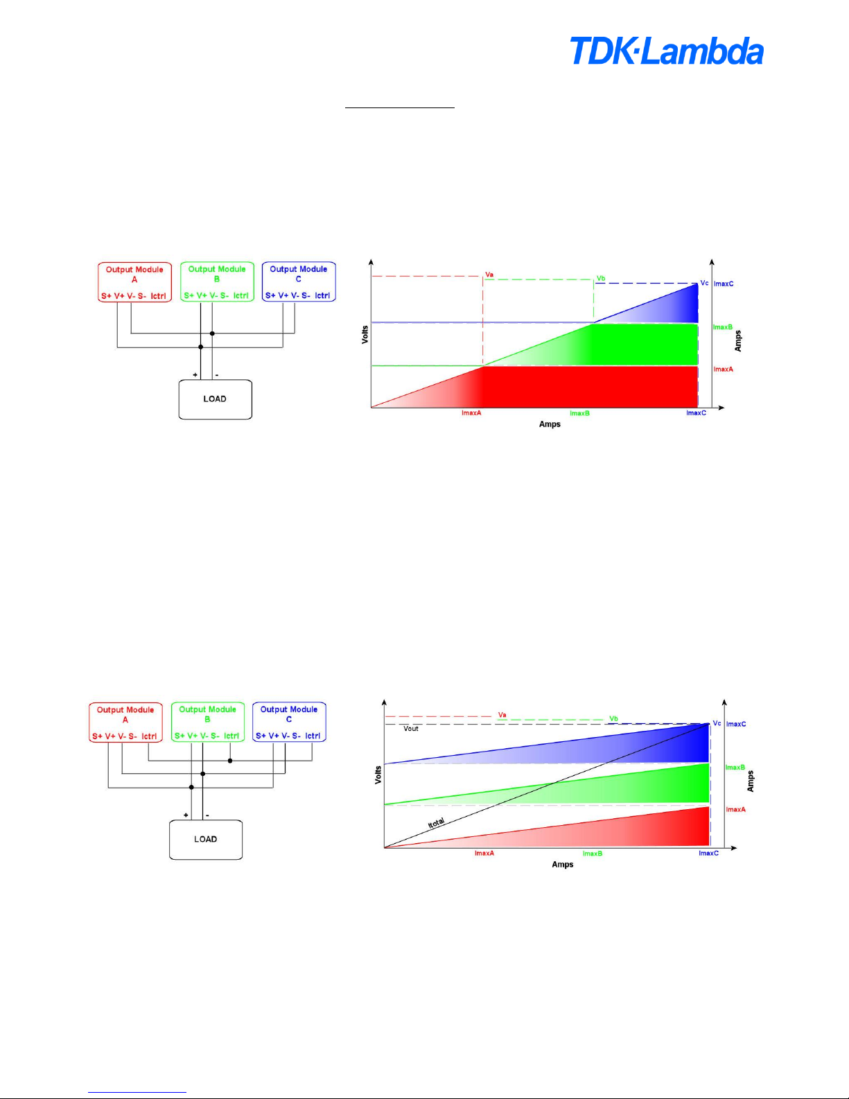
11. Parallel Connected Outputs
CM output modules of the same type can be paralleled within the same product to achieve higher output currents. Links for paralleling modules
are available directly from TDK-Lambda.
The following instructions must be followed for output modules configured in this manner.
When paralleled, the outputs can operate in two distinct modes, Normal parallel mode or Share parallel mode.
Normal Parallel Mode
For normal parallel mode, the positive power cables should be connected together and the negative power cables should be connected together.
No other connections are required as shown in the diagram below.
In this mode, the highest adjusted output module will supply all of the load current until its current limit is reached. If the load demand exceeds
this level the output voltage will drop to the level of the next highest adjusted module and that module will begin to supply the load current while
the first module continues delivering full current. This process repeats for the total number of paralleled modules. The diagram above shows the
VI curve for such a system.
Output modules that are not delivering current will typically sink a small amount of current from the other outputs, but this will not exceed -6% of
each module’s maximum rated current.
Typically, system reliability is reduced in this mode as the higher adjusted modules will do most of the work with the lower adjusted modules only
delivering current during peak load demand.
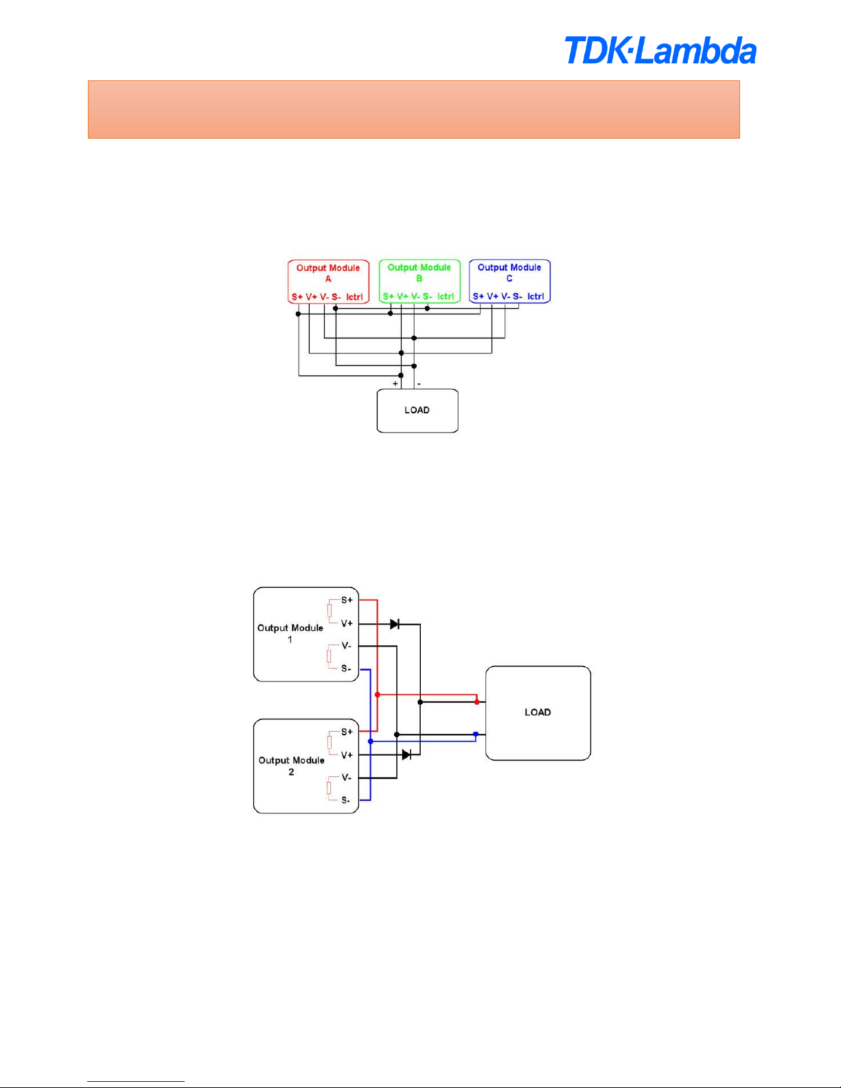
Share Parallel Mode
In share parallel mode, the outputs are paralleled as before and the I
CONTROL
pin of each module connected together as shown in the diagram
below.
Connecting the I
CONTROL
pins together forces all the outputs to deliver the same current, ensuring that the system reliability is maximised and the
work load is distributed evenly across all paralleled modules.
In this mode, the lowest adjusted output module will determine the actual output voltage and all higher adjusted outputs will reduce their voltage.
The current output signal (I
CONTROL
) can still be used to measure the output current but it must be scaled by N, where N is the number of
paralleled modules.
Page 22
CM4 App Note 260424 issue 2.1.docx Document No. 260424 Page 22 of 29
Parallel Remote Sensing
Remote sensing can be used as normal with paralleled modules. The sense lines (S+ and S-) from each of the output modules should be
connected together, S+ to S+, and S- to S- as shown below. This should be done close to the power supply output and a single pair of cables
brought from these sense lines to the load. Keeping cable lengths to a minimum and using twisted pairs where necessary will help reduce noise
pickup in the sense lines.
N+1 Configurations
When using N+1 redundant configurations, a suitably rated diode (or controlled MOSFET) must be used on each output to prevent a device
failure from causing a system failure. However, the diode introduces voltage drops between the supply and the load that significantly degrade the
load regulation. To counteract this, the remote sense lines can be used to regulate the voltage at the load as shown below.
Typically, this configuration can damage the internal sense resistors used within a power supply. However, the CM outputs have integrated
protection to prevent this type of damage and are completely N+1 compatible without any additional external protection circuitry. Note that only
the positive sense terminal is protected and diodes should be used in the positive connection only.
WARNING!
Care must be taken to avoid differential voltages between the negative power output terminals of share mode paralleled modules as this can cause
errors at the control pins. To avoid this, it is recommended to use TDK-Lambda parallel links to parallel modules in share mode.
Page 23
CM4 App Note 260424 issue 2.1.docx Document No. 260424 Page 23 of 29
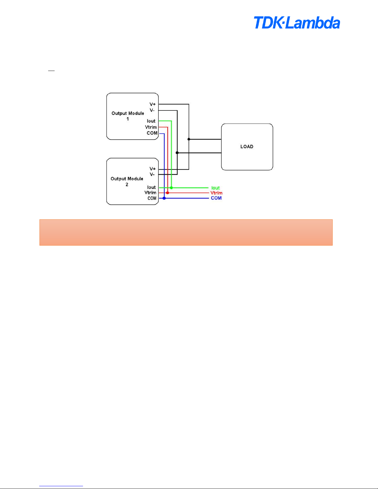
Paralleled Remote Voltage/Current Adjustments
The simplest way to achieve remote voltage/current programming with paralleled outputs is to operate the modules in share parallel mode.
Follow the procedure outlined earlier to configure the outputs in share parallel mode and once configured in this mode, all the V
CONTROL
and COM
pins can be connected together. Remote voltage/current programming can then be performed exactly as with a stand-alone module.
It is not recommended to use remote voltage/current programming in normal parallel mode.
Paralleling Across Multiple Products
Paralleling across multiple products is not possible without external protection (such as external diodes or controlled MOSFETs) to prevent
circulating currents between each product. Failure to provide such protection may result in damage to the power supplies. Consult TDK-Lambda
for details on how best to implement such applications.
When modules are paralleled across multiple products, the outputs in each product will not be synchronised and the peak to peak output ripple
may contain beat frequencies in the audio spectrum.
WARNING!
Care must be taken to avoid differential voltages between the negative power output terminals of share mode paralleled modules as this can cause
errors at the control pins. To avoid this, it is recommended to use TDK-Lambda parallel links to parallel modules in share mode.
Page 24
CM4 App Note 260424 issue 2.1.docx Document No. 260424 Page 24 of 29
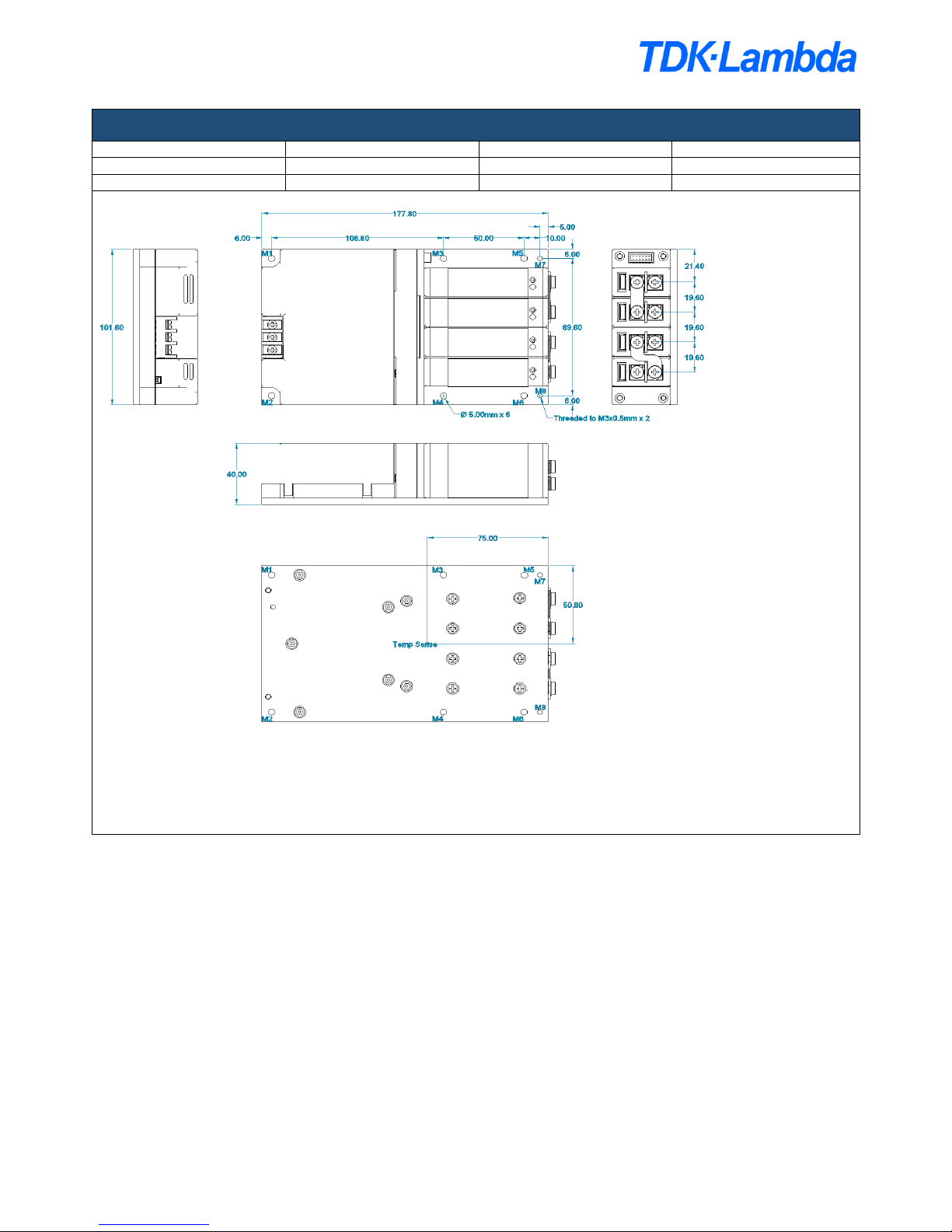
12. Mechanical Dimensions and Mounting
SCREWS
Location
Details
Penetration
Tightening
Baseplate Mount: M1 – M6
Hole size, Diameter 5.00mm
4mm Baseplate thickness
0.55 NM
Output Module Connection
M4
-
0.35 NM
Input Module Connection
6-32
-
0.8 NM
Unless stated otherwise, all dimensions are in millimeter s and in accordance with DIN2768 -1/2 CLASS C
Page 25

CM4 App Note 260424 issue 2.1.docx Document No. 260424 Page 25 of 29
13. Connector details
PINOUTS
Circuit
Details
J1 – Mains Input
1
Live
2
Neutral
3
Earth
J2 – Standby control
1 Standby control negative
2 Standby control positive
J3 – Global Signals
1 Slot 4 - Power Good
2
Slot 4 - Inhibit
3 Slot 3 - Power Good
4
Slot 3 - Inhibit
5 Slot 2 - Power Good
6
Slot 2 - Inhibit
7 Slot 1 - Power Good
8
Slot 1 - Inhibit
9 Temperature sense (T
SNS
)
10
AC OK
11
+5V (Bias Supply 1A)
12
COM
J4 -Output Signals
1
- Sense
2
+ Sense
3
COM
4
I Control
5
V Control
6
+5V (Bias Supply 10mA)
MATING CONNECTORS
Ref.
Details
Manufacturer
Housing
Terminal
J1 - Mains Input
3 Pin, Barrier, 6-32 Steel Screws, 0.8 Nm or 7 Lb-In Torque
(1)
J2 - Standby control
2 Pin, 1.25mm, with Friction Lock, 28-30AWG
MOLEX
0510210200
0500588000
J3 - Global Signals
12 Pin, 2mm, with Friction Lock, 24-30 AWG, WIRE TO BOARD
MOLEX
0511101260
0503948051
12 Pin, 2mm, with Friction Lock, 24-30 AWG, IDT CABLE TO BOARD
MOLEX
0875681273
J4 - Output Signals
6 PIN, 1.25mm, with Friction Lock, 28-30AWG
MOLEX
0510210600
0500588000
Output Power
Positive/Negative, M4 terminal, use appropriately rated crimp terminal
Notes 1. Cable 14-18AWG, 300V, 16A, 105°C, use appropriately rated crimp terminal.
2. Direct equivalents may be used for any connector parts.
3. All cables must be rated 105°C min, equivalent to UL1015
Page 26

CM4 App Note 260424 issue 2.1.docx Document No. 260424 Page 26 of 29
14. EMC Compliance
Typical Conducted emissions
Typical Radiated emissions
For radiated and conducted emissions, compliance of the final system relies on proper installation of the PSU component. The installation
guidelines detailed below should be followed.
Installation Guidelines for optimum EMC performance
CM units should be mounted within a metal enclosure using the mounting fixtures provided.
If the application enclosure is not metal, then a metal ground plate should be used to mount both the power supply and the load.
Both input and output cables should be fixed as close as possible to the ground plate or metal enclosure.
Input and output cables should be separated as much as possible from each other or a shield/screen used to isolate RF currents
Output power and sense cables should be twisted pairs and routed parallel to each other. Do not twist sense and power cables
together.
All cables lengths and loop areas should be minimised.
Where cables must enter or exit the enclosure, good high frequency 100nF decoupling capacitors of sufficient voltage rating should be
connected to the cables as close to the entry/exit point as possible.
For further details or assistance contact TDK-Lambda.
Page 27

CM4 App Note 260424 issue 2.1.docx Document No. 260424 Page 27 of 29
15. Reliability
The CM4 series has undergone extensive testing, including HALT and Environmental testing. Reliability data is collected on an ongoing basis.
Please contact TDK-Lambda for the most up to date reliability data.
The reliability data quoted in the datasheets are the calculated failures per million hours (FPMH) using the Telcordia SR-332, issue 2 standard.
The procedure defined in SR-332 allows several different techniques to be used for calculating MTBF and when evaluating competing MTBF
figures it is important that only the same techniques are compared.
The quoted CM reliability figures use Method I Case 3, Ground, Fixed, Controlled which specifies an ambient temperature of 30°C and an upper
confidence level of 90%. It is also assumed that the product is operated at 100% duty cycle, has an input voltage of 220V
RMS
, an output power of
600W and that the baseplate temperature is the same as the ambient temperature.
The table below shows a summary of the FPMH & MTBF for all system components and for a typical fully assembled system.
Assembly
Failure Rate (FPMH)
MTBF (Hrs)
Input module
0.962972
1038452
Transformer
0.371919
2688754
S1
0.415368
2407499
S2
0.397808
2513774
S3
0.398170
2511487
S4
0.405630
2465300
CM4 with 4 S1 modules
2.996363
333737.934
To calculate the MTBF of any CM system,
Add the FPMH figures for each system component to give the total FPMH.
Get the MTBF by dividing 1,000,000 by the total FPMH.
The variation in FPMH is shown in the graph and table below.
Temp
Input module
Transformer
S1
S2
S3
S4
CM4 with 4 S1 modules
0
0.41329578
0.127619
0.192619
0.185396
0.186105
0.186243
1.291276945
10
0.54688976
0.178886
0.245347
0.235357
0.235992
0.2362
1.678671789
20
0.72397837
0.255159
0.316147
0.302737
0.30326
0.305183
2.206465072
30
0.96297168
0.371919
0.415369
0.397808
0.39817
0.40563
2.951868534
40
1.29407059
0.555049
0.560829
0.538309
0.538452
0.559393
4.046103211
50
1.76616217
0.846405
0.782692
0.754326
0.754185
0.803972
5.707742381
60
2.46010898
1.315415
1.130884
1.095712
1.095216
1.202005
8.299340054
70
3.50420104
2.067304
1.686039
1.643019
1.642101
1.855247
12.39791075
80
5.09894211
3.266645
2.575169
2.523173
2.52177
2.925702
18.91140128
90
7.55815578
5.160517
3.995269
3.93316
3.931214
4.659641
29.23795696
100
11.3495991
8.112606
6.236851
6.163284
6.160733
7.430093
45.4531658
Page 28

CM4 App Note 260424 issue 2.1.docx Document No. 260424 Page 28 of 29
16. Output Modules
Refer to datasheet for output module ratings
Adjusting output voltages
Each CM output module contains a built-in potentiometer to allow for accurate output voltage adjustments. To adjust the output voltage, connect
a calibrated voltmeter (or DMM) to the output terminals and insert an appropriate trimming tool (e.g. Bourns Model H-90, maximum diameter
3mm) through the hole marked “Adjust” at the top of the output module as shown below. Do not use excessive force as this may damage the unit.
Ensure the trimming tool mates correctly with the internal potentiometer and slowly turn the tool clockwise to increase the voltage or counterclockwise to decrease the voltage. Once the desired voltage has been achieved, remove the trimming tool and disconnect the voltmeter. Repeat
this step for each output module in need of adjustment.
Attaching a heatsink or cooling plate
For improved performance, the baseplate of the CM4 unit can be attached to a heatsink or cooling plate. TDK-Lambda has a range of heatsinks
available to allow the CM4 to be mounted horizontally or vertically.
Each heatsink comes pre-assembled with a high performance thermal interface pad and 6 x M4 x 10mm Pozi Pan screws which can be used to
attach the heatsink to the baseplate.
The diagrams below show a CM4 unit attachment to a Type 1 and Type 2 heatsink. Before assembly ensure both the baseplate and heatsink
surfaces are clean and free from debris. The final assembly can then be mounted into the end system via the four holes (Type 1: 2 each side,
Type 2: 2 each end) on the flange of the heatsink.
It is recommended to tighten the baseplate mounting screws to 0.55 NM. In high vibration environments, an appropriate thread lock should be
used.
All recommended screw tightening torques are nominal values and should be verified in the application where appropriate.
CM4 Heatsink 1
CM4 Heatsink 2
Voltage Adjust
Page 29

CM4 App Note 260424 issue 2.1.docx Document No. 260424 Page 29 of 29
17. Accessories
Description
Photo/Drawing
Part number*
Current share cables
2 way = 200451
3 way = 200452
4 way = 200451
Output
Cable Set
1x Signals cable
(~200mm)
2x Power terminals
200450
Input
Cable Set
1x Signals cable
(~200mm)
1x Standby cable
(~200mm)
3x Power terminals
200449
CM4 Heatsink1
(Provided with 6x M4 x
10mm Posi-Drive screws
for baseplate mounting
and thermal interface ACC-
TF)
200445
CM4 Heatsink2
(Provided with 6x M4 x
10mm Posi-Drive screws
for baseplate mounting
and thermal interface
200447)
200446
Thermal interface
(170mmx80mm)
200447
* For larger pack size part numbers, please contact TDK-Lambda.
4 WAY SHARE CABLE
 Loading...