

Page 1
(1/30)
AC Input
Conformity to RoHS Directive
Single Output, General-Purpose, UL/C-UL/TÜV Approved
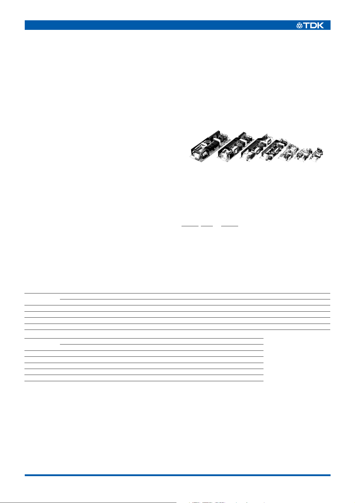
J Series JBW(10 to 150W)
FEATURES
• Compact and low price.
• Wide input voltage range.
• Safety standards approved.
• Corresponds to products with CE marking.
• Full lineup of output power 10 to 150W
• Open frame
• Meets conducted noise standard FCC Class B.
• Warranty period: 3 years
• Specific bromine inflammable materials (PBDPEs, PBBs) are
not included in use.
• It is a product conforming to RoHS directive.
APPLICATIONS
Measuring equipment, robotics, automation equipment, information processing equipment, security systems, amusement equipment, etc.
PRODUCT IDENTIFICATION
SAFETY STANDARDS
UL60950-1, CSA C22.2 No.60950-1(C-UL), EN60950-1(TÜV),
approved.
EMC REGULATIONS
• FCC Class-B, VCCI Class-B, EN-55011-B and EN55022-B
meet.
• Harmonic current requirement EN61000-3-2 meet(50 to 150W).
JBW 05 – 2R0
(1) (2) (3)
(1)Series name
(2)Rated output voltage
(3)Rated output current(R: Decimal point)
PART NUMBERS AND RATINGS
Output voltage
(V)
5 2 JBW05-2R0 3 JBW05-3R0 6 JBW05-6R0 10 JBW05-10R
12 0.9 JBW12-0R9 1.3 JBW12-1R3 2.5 JBW12-2R5 4.3 JBW12-4R3
15 0.7 JBW15-0R7 1 JBW15-1R0 2 JBW15-2R0 3.5 JBW15-3R5
24 0.5 JBW24-0R5 0.7 JBW24-0R7 1.3 JBW24-1R3 2.1 JBW24-2R1
Output voltage
(V)
5 15 JBW05-15R 20 JBW05-20R 30 JBW05-30R
12 6.3 JBW12-6R3 8.5 JBW12-8R5 12.5 JBW12-12R
15 5.0 JBW15-5R0 6.7 JBW15-6R7 10 JBW15-10R
24 3.2 JBW24-3R2 4.3 JBW24-4R3 6.3 JBW24-6R3
48 —— —— 3.2JBW48-3R2
• 3.3 and 48V models(75 to 150W type) are made to order.
• Conformity to RoHS Directive: This means that, in conformity with EU Directive 2002/95/EC, lead, cadmium, mercury, hexavalent chromium, and specific
bromine-based flame retardants, PBB and PBDE, have not been used, except for exempted applications.
10W Type 15W Type 30W Type 50W Type
Current(A) Part No. Current(A) Part No. Current(A) Part No. Current(A) Part No.
75W Type 100W Type 150W Type
Current(A) Part No. Current(A) Part No. Current(A) Part No.
• All specifications are subject to change without notice.
004-02 / 20070523 / ea122_jbw.fm
Page 2
(2/30)
JBW10W Type
SPECIFICATIONS AND STANDARDS
Part No. JBW05-2R0 JBW12-0R9 JBW15-0R7 JBW24-0R5
Rated output voltage and current
Maximum output power W 10 10.8 10.5 12
Input conditions
Input voltage Eac/Edc V 85 to 265[Rating: 100 to 240]/110 to 370
Input frequency Hz 47 to 440[Rating: 50 to 60](Single phase)
Input current A 0.25typ./0.35max. [AC.100V]0.15typ./0.25max.[AC.240V]
Fuse rating A 2[AC.250V, built-in]
Surge current A 15typ.(20max.)[AC.100V]30typ.(40max.)[AC.240V] 1st surge current, cold start, reset after 1s minimum.
Leakage current mA 0.1typ./0.75max.[AC.100V, 60Hz]0.15typ./0.75max.[AC.240V, 60Hz]
Power factor 0.6typ./0.45typ.[AC.100/240V]
Efficiency
Output characteristics
Output voltage Edc V 5 12 15 24
Voltage variable range Edc V Fixed Fixed Fixed Fixed
Maximum output current A 2 0.9 0.7 0.5
Minimum output currentA0000
Overvoltage threshold Edc V 5.75min. 13.8min. 17.25min. 27.6min.
Overcurrent threshold A 2.5min. 1.12min. 0.87min. 0.62min.
Source effect % 0.4max.[Within the input voltage range]
Voltage
stability
Ripple Ep-p mV 80max. 120max. 120max. 120max.
Ripple noise Ep-p mV 120max. 150max. 150max. 150max.
Start up time ms 700max.(200typ.)/700max.(200typ.) [AC.100/240V]
Hold up time ms 15typ/140typ [AC.100/240V]
Auxiliary functions
Indicator display No
Overvoltage protection Zenor diode clamp method, output may latch up depending on the condition.
Overcurrent protection Fold back type, automatic recovery.
Remote ON-OFF No
Remote sensing No
Parallel operation Impossible
Series operation Inpossible
Output voltage external variable function No
Standards
Safety standards UL60950-1, CSA C22.2 No.60950-1(C-UL), EN60950-1(TÜV) approved.
Noise terminal voltage FCC-B, VCCI-B, EN55011-B, EN55022-B meet.
Input harmonics current requirement No
Constructions
External dimensions mm 21× 36×95[H× W×L]
Weight g 50max.
Mounting method Can be attached to 1 side.
Case material No(PWB Material: CEM3)
∗
Current rating(maximum output current) is determined for –10 to +50°C. Derating is required when used outside this temperature range.
• Optional input, output cable kits are available at a separate price.
Load effect % 0.8max.[0 to 100% load]
Temperature effect % 1max.[Ambient temperature: –10 to +50°C]
Drift(Time effect) % 0.4max.[25°C, input and output ratings, after input voltage ON for 30min to 8h]
Recovery % ±4max.[50 to 100% sudden load change]
∗
5V • 2A 12V • 0.9A 15V • 0.7A 24V • 0.5A
% 71typ.[AC.100V] 78typ.[AC.100V] 79typ.[AC.100V] 82typ.[AC.100V]
% 71typ.[AC.240V] 79typ.[AC.240V] 80typ.[AC.240V] 83typ.[AC.240V]
• All specifications are subject to change without notice.
004-02 / 20070523 / ea122_jbw.fm
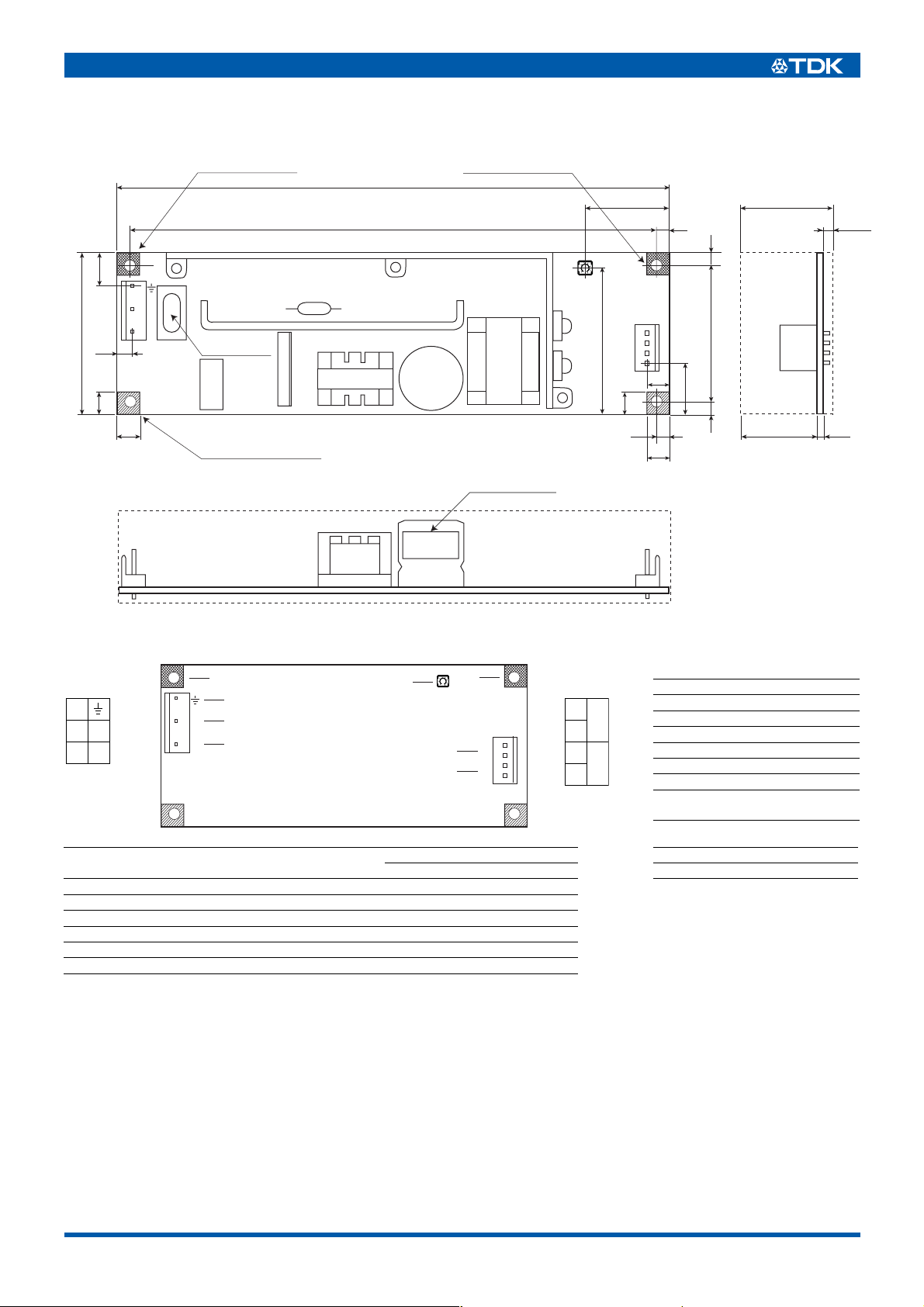
Page 3
JBW10W Type
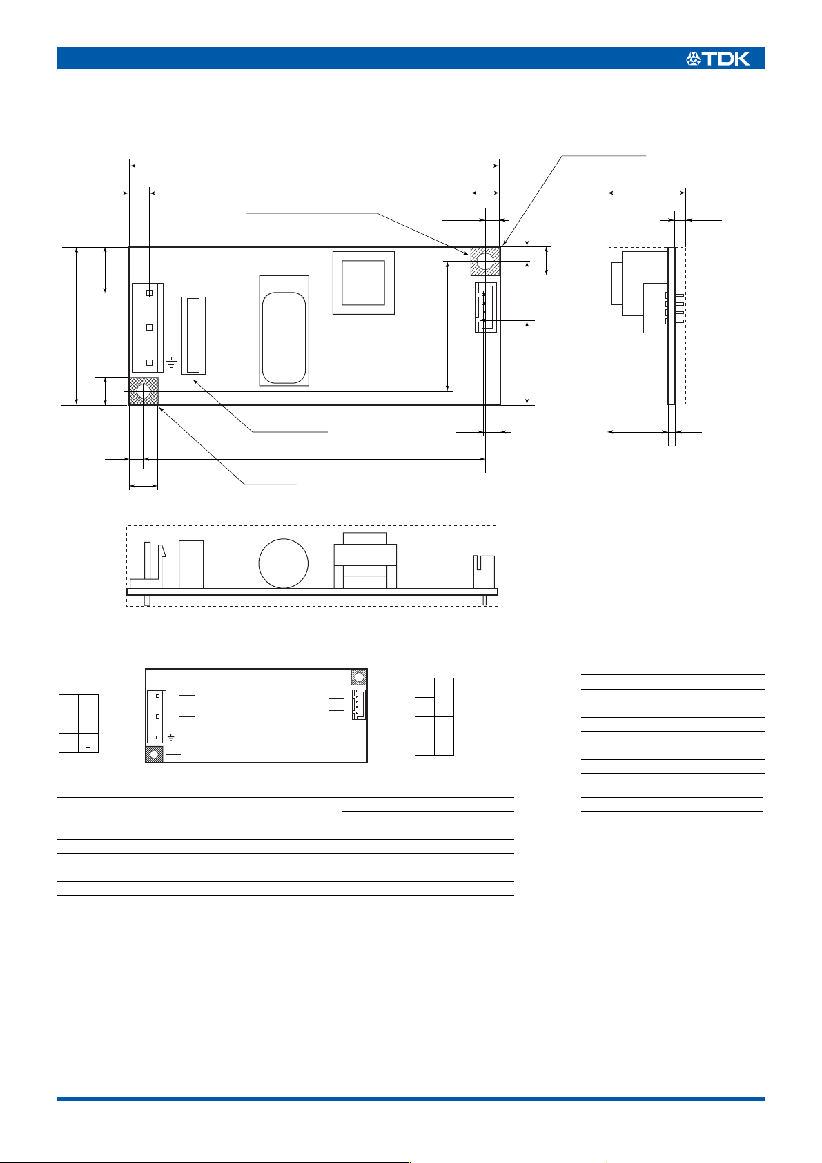
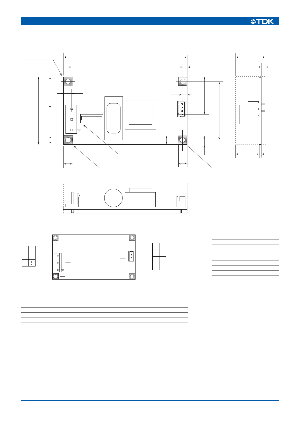
SHAPES AND DIMENSIONS
(3/30)
2-
95
ø3.4Mounting holes
21
3max.
16.4 1.6
3.5
29±0.5
TB2
3.8
7
3.5
7
+
+
_
_
17.3
5.2
Area For Spacer(
Solder Side
10
36
7
3.5
TB1
L
N
7
TDK
Ser. No. LABEL
GND Pad
Solder Side
ø6.0max.)
JBW05-2R0
88±0.5
Dimensions in mm
±1mm : without specified dimensions
TERMINAL DESIGNATION
TB2
TB1
P3
P2LN
P1
Connector made by
L
N
2
3
4
Power supply side
connector
+
6
+
_
_
5
Cable Side Option Part No.
Housing Terminal Set 4EU20G054
1
Japan Solderless Terminal Co., Ltd.
Input Connector(TB1) VH Series B3P5-VH-B VHR-5N SVH-21T-P1.1
Output Connector(TB2) XH Series B4B-XH-2 XHP-4 SXH-001T-P0.6
LCE
Input Connector(TB1) P101 Series P101-05-2/4 H101-05 T101
Output Connector(TB2) P221 Series P221-04 H221-04 T221-01
P4
P3
P2
P1
+
–
Terminal No. Designations
1 Input terminal(L)
2 Input terminal(N)
3 Frame ground terminal(G)
4 Ground pad
5 Output terminal(–)
6 Output terminal(+)
• All specifications are subject to change without notice.
004-02 / 20070523 / ea122_jbw.fm
Page 4
(4/30)
JBW15W Type
SPECIFICATIONS AND STANDARDS
Part No. JBW05-3R0 JBW12-1R3 JBW15-1R0 JAW24-0R7
Rated output voltage and current
Maximum output power W 15 15.6 15 16.8
Input conditions
Input voltage Eac/Edc V 85 to 265[Rating: 100 to 240]/110 to 370
Input frequency Hz 47 to 440[Rating: 50 to 60](Single phase)
Input current A 0.36typ./0.43max.[AC.100V]0.2typ./0.24max.[AC.240V]
Fuse rating A 2[AC.250V, built-in]
Surge current A 15typ./19.5max.[AC.100V]30typ./41max.[AC.240V] 1st surge current, cold start, reset after 1s minimum.
Leakage current mA 0.2typ./0.75max.[AC.100V, 60Hz]0.3typ./0.75max.[AC.240V, 60Hz]
Power factor 0.6typ./0.45typ.[AC.100/240V]
Efficiency
Output characteristics
Output voltage Edc V 5 12 15 24
Voltage variable range Edc V Fixed Fixed Fixed Fixed
Maximum output current A 3 1.3 1 0.7
Minimum output currentA0000
Overvoltage threshold Edc V 5.75min. 13.8min. 17.25min. 27.6min.
Overcurrent threshold A 3.15min. 1.37min. 1.05min. 0.74min.
Source effect % 0.4max.[Within the input voltage range]
Voltage
stability
Ripple Ep-p mV 80max. 120max. 120max. 120max.
Ripple noise Ep-p mV 120max. 150max. 150max. 150max.
Start up time ms 200max.(25typ.)/100max.(25typ.)[AC.100/240V] 200max.(40typ.)/100max.(40typ.)[AC.100/240V]
Hold up time ms 13typ./150typ. [AC.100/240V]
Auxiliary functions
Indicator display No
Overvoltage protection Zenor diode clamp method, output may latch up depending on the condition.
Overcurrent protection Rectangular type, automatic recovery.
Remote ON-OFF No
Remote sensing No
Parallel operation Impossible
Series operation Impossible
Output voltage external variable function No
Standards
Safety standards UL60950-1, CSA C22.2 No.60950-1(C-UL), EN60950-1(TÜV) approved.
Noise terminal voltage FCC-B, VCCI-B, EN55011-B, EN55022-B meet.
Input harmonics current requirement No
Constructions
External dimensions mm 22.6× 50× 95[H× W× L]
Weight g 80max.
Mounting method Can be attached to 1 side.
Case material No(PWB Material: CEM3)
∗
Current rating(maximum output current) is determined for –10 to +50°C. Derating is required when used outside this temperature range.
• Optional input, output cable kits are available at a separate price.
Load effect % 0.8max.[0 to 100% load]
Temperature effect % 1max.[Ambient temperature: –10 to +50°C]
Drift(Time effect) % 0.4max.[25°C, input and output ratings, after input voltage ON for 30min to 8h]
Recovery % ±4max.[50 to 100% sudden load change]
∗
5V • 3A 12V • 1.3A 15V • 1.0A 24V • 0.7A
% 72typ.[AC.100V] 76typ.[AC.100V] 76typ.[AC.100V] 78typ.[AC.100V]
% 72typ.[AC.240V] 74typ.[AC.240V] 74typ.[AC.240V] 76typ.[AC.240V]
• All specifications are subject to change without notice.
004-02 / 20070523 / ea122_jbw.fm
Page 5
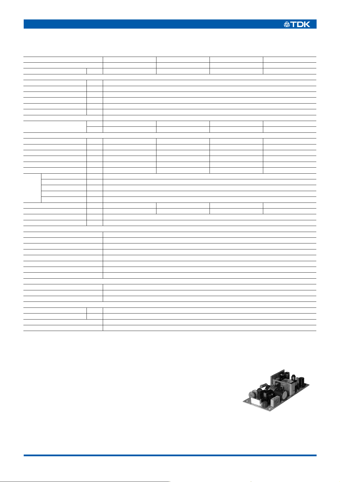
JBW15W Type
SHAPES AND DIMENSIONS
ø
3.4Mounting holes
4-
95
88±0.5
3.5
(5/30)
22.6
3max.
23.7
50
7
7
TERMINAL DESIGNATION
TB1
N
5.2
L
TDK
GND Pad
Solder Side
JBW05-3R0
Ser. No. LABEL
3.8
+
+
_
_
TB3
7
7
28
43±0.5
3.5
Area For Spacer (ø6.0max.)
Solder Side 3 Places
18.5
1.6
Dimensions in mm
±1mm : without specified dimensions
TB1
P3
P2LN
P1
Connector made by
+
1
L
2
N
3
4
Power supply side
connector
6
+
_
5
_
Cable Side Option Part No.
Housing Terminal Set 4EU20G054
P4
P3
P2
P1
TB3
+
–
Japan Solderless Terminal Co., Ltd.
Input Connector(TB1) VH Series B3P5-VH-B VHR-5N SVH-21T-P1.1
Output Connector(TB3) XH Series B4B-XH-2 XHP-4 SXH-001T-P0.6
LCE
Input Connector(TB1) P101 Series P101-05-2/4 H101-05 T101
Output Connector(TB3) P221 Series P221-04 H221-04 T221-01
Terminal No. Designations
1 Input terminal(L)
2 Input terminal(N)
3 Frame ground terminal(G)
4 Ground pad
5 Output terminal(–)
6 Output terminal(+)
• All specifications are subject to change without notice.
004-02 / 20070523 / ea122_jbw.fm
Page 6
(6/30)
JBW30W Type
SPECIFICATIONS AND STANDARDS
Part No. JBW05-6R0 JBW12-2R5 JBW15-2R0 JAW24-1R3
Rated output voltage and current
Maximum output power W 30 30 30 31.2
Input conditions
Input voltage Eac/Edc V 85 to 265[Rating: 100 to 240]/110 to 370
Input frequency Hz 47 to 440[Rating: 50 to 60](Single phase)
Input current A 0.65typ./0.86max.[AC.100V]0.35typ./0.48max.[AC.240V]
Fuse rating A 2[AC.250V, built-in]
Surge current A 15typ./30max.[AC.100V]30typ./60max.[AC.240V] 1st surge current, cold start, reset after 1s minimum.
Leakage current mA 0.35typ./0.75max.[AC.100V, 60Hz]0.5typ./0.75max.[AC.240V, 60Hz]
Power factor 0.6typ./0.45typ.[AC.100/240V]
Efficiency
Output characteristics
Output voltage Edc V 5 12 15 24
Voltage variable range Edc V Fixed Fixed Fixed Fixed
Maximum output current A 6 2.5 2 1.3
Minimum output currentA0000
Overvoltage threshold Edc V 5.6min. 13.3min. 16.6min. 26.5min.
Overcurrent threshold A 6.3min. 2.7min. 2.1min. 1.4min.
Source effect % 0.4max.[Within the input voltage range]
Voltage
stability
Ripple Ep-p mV 80max. 120max. 120max. 120max.
Ripple noise Ep-p mV 120max. 150max. 150max. 150max.
Start up time ms 650max.(350typ.)/320max.(130typ.)[AC.100/240V]
Hold up time ms 20typ./160typ.[AC.100/240V]
Auxiliary functions
Indicator display No
Overvoltage protection Voltage shut-down type.
Overcurrent protection Rectangular type(Winker operation), automatic recovery.
Remote ON-OFF No
Remote sensing No
Parallel operation Impossible
Series operation Impossible
Output voltage external variable function No
Standards
Safety standards UL60950-1, CSA C22.2 No.60950-1(C-UL), EN60950-1(TÜV) approved.
Noise terminal voltage FCC-B, VCCI-B, EN55011-B, EN55022-B meet.
Input harmonics current requirement No
Constructions
External dimensions mm 26× 55×122[H× W× L]
Weight g 150max.
Mounting method Can be attached to 1 side.
Case material No(PWB Material: CEM3)
∗
Current rating(maximum output current) is determined for –10 to +50°C. Derating is required when used outside this temperature range.
• Optional input, output cable kits are available at a separate price.
Load effect % 0.8max.[0 to 100% load]
Temperature effect % 2max.[Ambient temperature: –10 to +50°C]
Drift(Time effect) % 0.4max.[25°C, input and output ratings, after input voltage ON for 30min to 8h]
Recovery % ±4max.[50 to 100% sudden load change]
∗
5V • 6A 12V • 2.5A 15V • 2A 24V • 1.3A
% 75typ.[AC.100V] 78typ.[AC.100V] 79typ.[AC.100V] 80typ.[AC.100V]
% 77typ.[AC.240V] 79typ.[AC.240V] 80typ.[AC.240V] 81typ.[AC.240V]
• All specifications are subject to change without notice.
004-02 / 20070523 / ea122_jbw.fm
Page 7
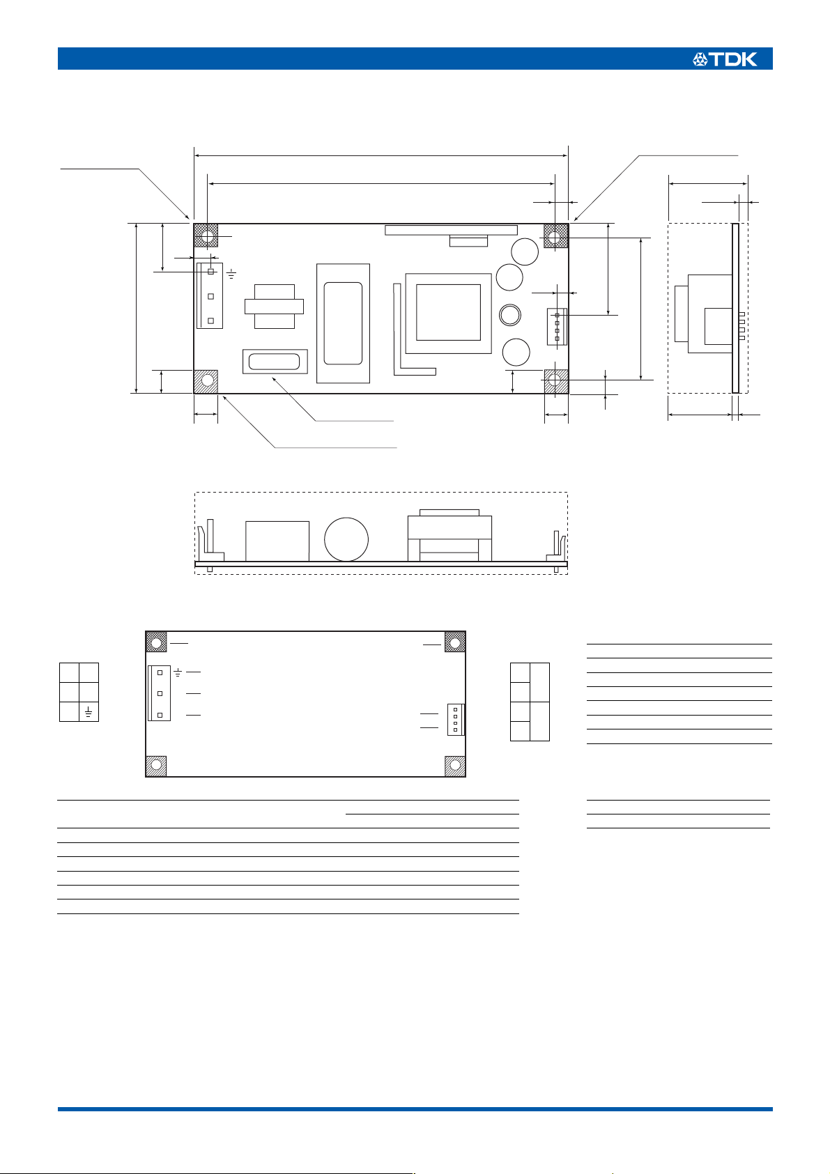
JBW30W Type
SHAPES AND DIMENSIONS
GND Pad 2 Places
Solder Side
16
6.5
55
TB1
N
L
TDK
122
112±0.5
JBW05-6R0
5
6.6
TB2
(7/30)
4-ø3.4Mounting holes
26
3max.
30
_
_
+
+
45±0.5
8
TERMINAL DESIGNATION
TB1
P1P2L
N
P3
4
N
L
8
8
Area For Spacer (
Solder Side 2 Places
Ser. No. LABEL
ø
6.0max.)
8
5
21.4 1.6
Dimensions in mm
±1mm : without specified dimensions
4
3
2
1
_
_
5
+
6
+
P1
P2
P3
P4
TB2
–
+
Terminal No. Designations
1 Input terminal(L)
2 Input terminal(N)
3 Frame ground terminal(G)
4 Ground pad
5 Output terminal(–)
6 Output terminal(+)
Connector made by
Power supply side
connector
Cable Side Option Part No.
Housing Terminal Set 4EU20G057
Japan Solderless Terminal Co., Ltd.
Input Connector(TB1) VH Series B3P5-VH-B VHR-5N SVH-21T-P1.1
Output Connector(TB2) VH Series B4P-VH-B VHR-4N SVH-21T-P1.1
LCE
Input Connector(TB1) P101 Series P101-05-2/4 H101-05 T101
Output Connector(TB2) P101 Series P101-04 H101-04 T101
• All specifications are subject to change without notice.
004-02 / 20070523 / ea122_jbw.fm
Page 8
(8/30)
JBW50W Type
SPECIFICATIONS AND STANDARDS
Part No. JBW05-10R JBW12-4R3 JBW15-3R5 JBW24-2R1
Rated output voltage and current
Maximum output power W 50 51.6 52.5 50.4
Input conditions
Input voltage Eac/Edc
Input frequency Hz 47 to 66[Rating: 50 to 60](Single phase)
Input current A 0.7typ./0.88max. [AC.100V]0.35typ./0.5max.[AC.240V]
Fuse rating A 3.15[AC.250V, built-in]
Surge current A 15typ.(30max.)[AC.100V]40typ.(60max.)[AC.240V] cold start
Leakage current mA 0.35typ./0.75max.[AC.100V, 60Hz]0.5typ./0.75max.[AC.240V, 60Hz]
Power factor 0.99typ./0.93typ.[AC.100/240V]
Efficiency
Output characteristics
Output voltage Edc V 5 12 15 24
Voltage variable range Edc V 4.5 to 5.5 10.8 to 13.2 13.5 to 16.5 21.6 to 26.4
Maximum output current A 10 4.3 3.5 2.1
Minimum output currentA0000
Overvoltage threshold Edc V 5.75 to 6.9 13.8 to 16.8 17.2 to 21 27.6 to 33.6
Overcurrent threshold A 10.5min. 5.4min. 4.4min. 2.7min.
Source effect % 0.4max.[Within the input voltage range]
Voltage
stability
Ripple Ep-p mV 80max. 120max. 120max. 120max.
Ripple noise Ep-p mV 120max. 150max. 150max. 150max.
Start up time ms 500max.(400typ.)/500max.(400typ.) [AC.100/240V]
Hold up time ms 20typ./20typ. [AC.100/240V]
Auxiliary functions
Indicator display No
Overvoltage protection Voltage shut-down type.
Overcurrent protection Rectangular type, automatic recovery.
Remote ON-OFF No
Remote sensing No
Parallel operation Impossible
Series operation Possible
Output voltage external variable function No
Standards
Safety standards UL60950-1, CSA C22.2 No.60950-1(C-UL), EN60950-1(TÜV) approved.
Noise terminal voltage FCC-B, VCCI-B, EN55011-B, EN55022-B meet.
Input harmonics current requirement EN61000-3-2 meet.
Constructions
External dimensions mm 26× 55×190[H× W× L]
Weight g 220max.
Mounting method Can be attached to 1 side.
Case material No(PWB Material: CEM3)
∗1
∗2
• Optional input, output cable kits are available at a separate price.
Load effect % 0.8max.[0 to 100% load]
Temperature effect % 1max.[Ambient temperature: –10 to +50°C]
Drift(Time effect) % 0.4max.[25°C, input and output ratings, after input voltage ON for 30min to 8h]
Recovery % ±4max.[50 to 100% sudden load change]
Current rating(maximum output current) is determined for –10 to +50°C. Derating is required when used outside this temperature range.
Please note that the deterioration of parts is occasionally caused when operating for a long time(over 10 minutes) with the voltage below the range of the
input voltage.
∗2
∗1
5V • 10A 12V • 4.3A 15V • 3.5A 24V • 2.1A
V 85 to 265[Rating: 100 to 240]/120 to 375
% 77typ.[AC.100V] 80typ.[AC.100V] 80typ.[AC.100V] 81typ.[AC.100V]
% 79typ.[AC.240V] 81typ.[AC.240V] 81typ.[AC.240V] 83typ.[AC.240V]
• All specifications are subject to change without notice.
004-02 / 20070523 / ea122_jbw.fm
Page 9
JBW50W Type
SHAPES AND DIMENSIONS
GND Pad 2 Places
Solder Side
12.18
190
180±0.5
4-ø4 Mounting holes
35.7
(9/30)
26
5
5
3max.
N
55
5.5
L
TB1
8
Ser. No. LABEL
Area For Spacer (
TERMINAL DESIGNATION
TB1
P3
P2 N
P1
L
4
N
L
Solder Side 2 Places
ø6max.)
3
2
1
JBW05-10R
TDK
7
4
5
6
RATING LABEL
_
_
+
+
P4
P3
P2
P1
TB2
–
+
47.7
TB2
_
_
+
+
7.1
8
5
8
45±0.5
17.2
5
±1mm : without specified dimensions
Terminal No. Designations
1 Input terminal(L)
2 Input terminal(N)
3 Frame ground terminal(G)
4 Ground pad
5 Output terminal(–)
6 Output terminal(+)
7
Output voltage variable
volume
1.621.4
Dimensions in mm
Connector made by
Power supply side
connector
Cable Side Option Part No.
Housing Terminal Set 4EU20G057
Japan Solderless Terminal Co., Ltd.
Input Connector(TB1) VH Series B3P5-VH-B VHR-5N SVH-21T-P1.1
Output Connector(TB2) VH Series B4P-VH-B VHR-4N SVH-21T-P1.1
LCE
Input Connector(TB1) P101 Series P101-05-2/4 H101-05 T101
Output Connector(TB2) P101 Series P101-04 H101-04 T101
• All specifications are subject to change without notice.
004-02 / 20070523 / ea122_jbw.fm
Page 10

JBW75W Type
SPECIFICATIONS AND STANDARDS
Part No. JBW05-15R JBW12-6R3 JBW15-5R0 JBW24-3R2
Rated output voltage and current 5V • 15A 12V • 6.3A 15V • 5.0A 24V • 3.2A
Maximum output power W 75 75.6 75 76.8
Input conditions
Input voltage Eac/Edc V 85 to 265[Rating: 100-240]/120 to 370
Input frequency Hz 47 to 66
Input current A 1.6/0.8max.[100-240V]
Fuse rating A 3.15
Surge current A 30/60max.[100-240V]
Leakage current mA 0.75/0.75max.[AC.100V(DENAN)/240V(UL, IEC)]
Power factor 0.99/0.95typ.[100-240V]
Efficiency %
Output characteristics
Output voltage Edc V 5 12 15 24
Voltage variable range Edc V 4.5 to 5.5 10.8 to 13.2 13.5 to 16.5 21.6 to 26.4
Maximum output current A 15 6.3 5.0 3.2(Peak4.2)
Overvoltage threshold Edc V 5.75 to 6.9 13.8 to 16.8 17.2 to 21 27.6 to 33.6
Overcurrent threshold A 15.8min. 6.6min. 5.2min. 4.4min.
Source effect % 0.4max.[Within the input voltage range]
Voltage
stability
Ripple Ep-p mV 80 120 120 120
Ripple noise Ep-p mV 120 150 150 150
Start up time ms 500max.(400typ.)/250max.(200typ.)[AC.100/240V]
Hold up time ms 20typ.[100-240V]
Auxiliary functions
Indicator display No
Overvoltage protection Voltage shut-down type(Latch).
Overcurrent protection Rectangular type, automatic recovery.
Remote ON-OFF No
Remote sensing No
Standards
Safety standards UL60950-1, CSA C22.2 No.60950-1(C-UL), EN60950-1(TÜV) approved.
Noise terminal voltage FCC-B, VCCI-B, EN55011-B, EN55022-B meet.
Input harmonics current requirement EN61000-3-2
CE marking Planned compliance.
Constructions
External dimensions mm 32× 55×222[H× W× L]
Weight g 290max.
Mounting method Can be attached to 1 side.
Case material CEM3
Load effect % 0.8max.[0 to 100% load]
Temperature effect % 1max.[Ambient temperature: –10 to +60°C]
Drift(Time effect) % 0.4max.[25°C, input and output ratings, after input voltage ON for 30min to 8h]
Recovery % ±4max.[50 to 100% sudden load change]
75/77typ.
[100-240V]
78/80typ.
[100-240V]
79/81typ.
[100-240V]
82/84typ.
[100-240V]
(10/30)
• All specifications are subject to change without notice.
004-02 / 20070523 / ea122_jbw.fm
Page 11

JBW75W Type
SHAPES AND DIMENSIONS
5 5
55 45±0.5
222
212±0.5
(11/30)
29
3max.1.6
4-ø3.5
5
3
CP1
55
(
5.3
)
25.9
(
9max.
1
)
9max.
Area for spacer(ø6max.
Solder Side(2 Places
)
)
Ground pattern area(ø6max.
Solder Side(2 Places
TERMINAL DESIGNATION
CP1
P1
L
P3 N
P5
· Japan Solderless Terminal Co., Ltd.
VH Series B3P5-VH-B
Connector made by
Japan Solderless Terminal Co., Ltd.
Input Connector(CP1)VH Series B3P5-VH-B VHR-5N SVH-21T-P1.1
Output Connector(CP2)VH Series B6P-VH-B VHR-6N SVH-21T-P1.1
5
3
CP1
1
Power supply side
connector
1
2
3
CP2
4
5
6
Cable Side Option Part No.
Housing Terminal Set 4EU20G085
(
)
4.5
1
CP2
6
(
)
45.9
)
)
CP2
P1
–
P2
P3
P4
+
P5
P6
· Japan Solderless Terminal Co., Ltd.
VH Series B6P-VH-B
)
)
50.9
(
)
43.2
(
33
(
±1mm : without specified dimensions
Dimensions in mm
• All specifications are subject to change without notice.
004-02 / 20070523 / ea122_jbw.fm
Page 12

JBW100W Type
SPECIFICATIONS AND STANDARDS
Part No. JBW05-20R JBW12-8R5 JBW15-6R7 JBW24-4R3
Rated output voltage and current 5V • 20A 12V • 8.5A 15V • 6.7A 24V • 4.3A
Maximum output power W 100 102 100.5 103.2
Input conditions
Input voltage Eac/Edc V 85 to 265[Rating: 100-240]/120 to 370
Input frequency Hz 47 to 66
Input current A 1.8/1.0max.[100-240V]
Fuse rating A 5
Surge current A 30/60max.[100-240V]
Leakage current mA 0.75/0.75max.[AC.100V(DENAN)/240V(UL, IEC)]
Power factor 0.99/0.95typ.[100-240V]
Efficiency %
Output characteristics
Output voltage Edc V 5 12 15 24
Voltage variable range Edc V ±10% ±10% ±10% ±10%
Maximum output current A 20 8.5 6.7 4.3(Peak5)
Overvoltage threshold Edc V 5.75 to 6.9 13.8 to 16.8 17.2 to 21 27.6 to 33.6
Overcurrent threshold A 21.0min. 10.6min. 8.38min. 5.38min.
Source effect % 0.4max.[Within the input voltage range]
Voltage
stability
Ripple Ep-p mV 80 120 120 120
Ripple noise Ep-p mV 120 150 150 150
Start up time ms 500max.(400typ.)/500max.(300typ.)[AC.100/240V]
Hold up time ms 20typ.[100-240V]
Auxiliary functions
Indicator display No
Overvoltage protection Voltage shut-down type(Latch).
Overcurrent protection Rectangular type, automatic recovery.
Remote ON-OFF No
Remote sensing No
Standards
Safety standards UL60950-1, CSA C22.2 No.60950-1(C-UL), EN60950-1(TÜV) approved.
Noise terminal voltage FCC-B, VCCI-B, EN55011-B, EN55022-B meet.
Input harmonics current requirement EN61000-3-2
CE marking Planned compliance.
Constructions
External dimensions mm 35× 62×222[H× W× L]
Weight g 400max.
Mounting method Can be attached to 1 side.
Case material FR4
Load effect % 0.8max.[0 to 100% load]
Temperature effect % 1max.[Ambient temperature: –10 to +60°C]
Drift(Time effect) % 0.4max.[25°C, input and output ratings, after input voltage ON for 30min to 8h]
Recovery % ±4max.[50 to 100% sudden load change]
78/80typ.
[100-240V]
80/82typ.
[100-240V]
80/82typ.
[100-240V]
82/85typ.
[100-240V]
(12/30)
• All specifications are subject to change without notice.
004-02 / 20070523 / ea122_jbw.fm
Page 13

JBW100W Type
SHAPES AND DIMENSIONS
5.0
62
)
52±0.5
17.9
(
(
4.7
5
)
CP1
3
1
Input
connector
222
212±0.5
Output voltage
adjustment trimmer
CP2
(13/30)
32
9
(
)
5.8
1
8
42.0
)
51.5
(
3max.1.6
5
9max.
9max.
Area for spacer(ø6max.
Solder Side(3 Places
)
)
Output voltage connector
Ground pattern area(ø6max.
Solder Side(1 Place
)
TERMINAL DESIGNATION
4
7
3
5
2
3
CP1
P1
L
P3 N
P5
· Japan Solderless Terminal Co., Ltd.
VH Series B3P5-VH-B
1
CP1
1
Connector made by
Power supply side
connector
CP2
· Japan Solderless Terminal Co., Ltd.
VH Series B8P-VH-B
Cable Side Option Part No.
Housing Terminal Set 4EU20G056
1
5
6
8
Japan Solderless Terminal Co., Ltd.
Input Connector(CP1)VH Series B3P5-VH-B VHR-5N SVH-21T-P1.1
Output Connector(CP2)VH Series B8P-VH-B VHR-8N SVH-21T-P1.1
CP2
P1
P2
P3
P4
P5
P6
P7
P8
(
)
32.7
)
±1mm : without specified dimensions
Dimensions in mm
Terminal No. Designations
–
1 Input terminal(L)
2 Input terminal(N)
3 Frame ground terminal(G)
4 Ground pad
5 Output terminal(–)
+
6 Output terminal(+)
7 Output voltage setting trim(+)
• All specifications are subject to change without notice.
004-02 / 20070523 / ea122_jbw.fm
Page 14

(14/30)
JBW150W Type
SPECIFICATIONS AND STANDARDS
Part No. JBW05-30R JBW12-12R JBW15-10R JBW24-6R3 JBW48-3R2
Rated output voltage and current
Maximum output power W 150 150 150 151.2 153.6
Input conditions
Input voltage Eac/Edc V 85 to 265[Rating: 100-240]/120 to 370
Input frequency Hz 47 to 66
Input current A 2.7/1.5max.[100-240V]
Surge current A 30/60max.[100-240V]
Leakage current mA 0.75/0.75max.[AC.100V(DENAN)/240V(UL, IEC)]
Power factor 0.99/0.95typ.[100-240V]
Efficiency %
Output characteristics
Output voltage EdcV5 12152448
Voltage variable range Edc V 4.5 to 5.5 10.8 to 13.2 13.5 to 16.5 21.6 to 26.4 43.2 to 52.8
Maximum output current A 30 12.5 10 6.3(Peak7.5) 3.2
Overvoltage threshold Edc V 5.75 to 6.9 13.8 to 16.8 17.2 to 21 27.6 to 33.6 55.2 to 67.2
Overcurrent threshold A 31.5min. 15.7min. 12.5min. 7.87min. 3.36min.
Source effect % 0.4max.[Within the input voltage range]
Voltage
stability
Ripple Ep-p mV 80max. 120max. 120max. 120max. 150max.
Ripple noise Ep-p mV 120max. 150max. 150max. 150max. 350max.
Start up time ms 500max.(400typ.)/500max.(300typ.)[AC.100/240V]
Hold up time ms 25/35typ.[AC.100/240V]
Auxiliary functions
Indicator display No
Overvoltage protection Voltage shut-down type(Latch).
Overcurrent protection Rectangular type, automatic recovery.
Remote ON-OFF No
Remote sensing No
Standards
Safety standards UL60950-1, CSA C22.2 No.60950-1(C-UL), EN60950-1(TÜV) approved.
Noise terminal voltage FCC-B, VCCI-B, EN55011-B, EN55022-B meet.
Input harmonics current requirement EN61000-3-2
CE marking Meet.
Constructions
External dimensions mm 40× 75×222[H× W× L]
Weight g 550max.
Mounting method Can be attached to 1 side.
Case metal FR4
∗
Current rating(maximum output current) is determined for –10 to +40°C. Derating is required when used outside this temperature range.
Load effect % 0.8max.[0 to 100% load]
Temperature effect % 1max.[Ambient temperature: –10 to +60°C]
Drift(Time effect) % 0.4max.[25°C, input and output ratings, after input voltage ON for 30min to 8h]
Recovery % ±4max.[50 to 100% sudden load change]
∗
5V • 30A 12V • 12A 15V • 10A 24V • 6.3A 48V • 3.2A
78/80typ.
[100-240V]
81/83typ.
[100-240V]
81/83typ.
[100-240V]
82/84typ.
[100-240V]
82/84typ.
[100-240V]
• All specifications are subject to change without notice.
004-02 / 20070523 / ea122_jbw.fm
Page 15

JBW150W Type
SHAPES AND DIMENSIONS
5.0 212±0.5
)
5
(
222
(5)
(15/30)
37
3max.1.6
5
CP1
3
1
75
65±0.55
)
47.2
(
Input connector
9max.
UP
(4)
9max.
Area for spacer(ø6max.
Solder Side(3 Places
TERMINAL DESIGNATION
4
3
5
3
CP1
P1
P3 N
P5
· Japan Solderless Terminal Co., Ltd.
VH Series B3P5-VH-B
1
L
CP1
2
1
Output voltage adjustment trimmer
)
)
· Japan Solderless Terminal Co., Ltd.
VH Series B6P-VH-B
Ground pattern area(ø6max.
Solder Side(1 Place
1
5
CP3
7
1
6
CP2
7
6
P1
P2
P3
P4
P5
P6
CP2
1
)
CP3
CP2
)
4
(
(4)
(
)
)
CP3
P1
P2
P3
+
P4
P5
P6
P7
· Japan Solderless Terminal Co., Ltd.
VH Series B7P-VH-B
27.9
–
29.5
7
1
)(
6
32.7
(
)
±1mm : without specified dimensions
Dimensions in mm
Terminal No. Designations
1 Input terminal(L)
2 Input terminal(N)
3 Frame ground terminal(G)
4 Ground pad
5 –Output terminal(–)
6 +Output terminal(+)
7 Output voltage setting trim(+)
Connector made by
Power supply side
connector
Cable Side Option Part No.
Housing Terminal Set 4EU00G062
Japan Solderless Terminal Co., Ltd.
Input Connector(CP1)VH Series B3P5-VH-B VHR-5N SVH-21T-P1.1
Output Connector(CP2)VH Series B6P-VH-B VHR-6N SVH-21T-P1.1
Output Connector(CP3)VH Series B7P-VH-B VHR-7N SVH-21T-P1.1
• All specifications are subject to change without notice.
004-02 / 20070523 / ea122_jbw.fm
Page 16

Characteristics, Functions, and Applications
BLOCK DIAGRAMS
JBW10W/15W/30W TYPES
(16/30)
AC input
L
N
Input
filter
circuit
rectifier
circuit
current
limiting
circuit
Surge
Input
JBW50W TYPE
AC input
L
N
Surge
current
limiting
circuit
Input
filter
circuit
Input
smoothing
circuit
COMMON SPECIFICATIONS
Temperature and humidity
Operating(°C) –10 to +60
Temperature range
Humidity range
Vibration and shock
Vibration
Shock
Withstand voltage and insulation resistance
Withstand voltage
Insulation resistance
Operating available(°C) –20 to –10
Storage(°C) –30 to +75
Operating(%)RH
Storage(%)RH
5 to 10Hz All amplitude 10mm[3 directions, each 1h]
10 to 200Hz Acceleration 19.6m/s
Acceleration 10 to 50W: 588m/s
Pulse duration 11±5ms
Input terminal to ground terminal(G) Eac: 2kV, 1min[Normal temperature, normal humidity, cutout current 10mA]
Input terminal to output terminal Eac: 3kV, 1min[Normal temperature, normal humidity, cutout current 10mA]
Output terminal to ground terminal(G) Eac: 500V, 1min[Normal temperature, normal humidity, cutout current 10mA]
Input terminal to ground terminal(G)
Output terminal to ground terminal(G)
Input
smoothing
circuit
Boost-up
circuit
PFC
control
circuit
Overcurrent
detection
circuit
control circuit
Overcurrent
detection
circuit
Output rectifying
and
smoothing circuit
Power
switching
circuit
Drive
circuit
PWM
Power
switching
circuit
Drive
circuit
Control circuit
Output voltage
control circuit
Output rectifying
and
smoothing circuit
Overvoltage
detection circuit
Output voltage
control circuit
Overvoltage
protection
10 to 90[Maximum wet-bulb temperature: 35°C, without dewing]
2
(2G)[3 directions, each 1h]
2
(60G)[3 directions, each 3 times]/75 to 150W: 588m/s2(60G)[Sine wave]
Eac: 500V, 100MΩ min.[Normal temperature, normal humidity]Input terminal to output terminal
+
–
+
–
DC OUT
DC OUT
• All specifications are subject to change without notice.
004-02 / 20070523 / ea122_jbw.fm
Page 17

Characteristics, Functions, and Applications
(17/30)
10 to 50W TYPES
OUTPUT POWER-AMBIENT TEMPERATURE(DERATINGS)
100
80
70
60
40
Output power(%)
20
–20 –10 0 10 20 30 40 50 60 71
Available operating range
(outside of warranty)
Ambient temperature(˚C)
INSTALLATIONS
• Mounting the power supply at the four corners with metal spac-
ers (2 corners for 10W models).
• Maintain a min. 4mm clearance distance in order to satisfy insu-
lation and high voltage safety requirements.
• Lay an insulating sheet under the power supply in case a min.
8mm installation space cannot be secured between the PC
board and the housing.
• Provide a min. 4mm distance between heat sink or component
surface and surrounding objects in order to cause a thermal convection.
• Since components are mounted on the back (solder) side of the
product, sufficient care should be taken when handling the
power supply to protect the PC board from shock, vibration, torsion, etc. which can result in damage caused by cracked chip
components.
75 to 150W TYPES
OUTPUT POWER-AMBIENT TEMPERATURE(DERATINGS)
75, 100W TYPES
100
80
60
40
Output power(%)
20
0
–20 –10
Available operating range
(outside of warranty)
0102030405060
Ambient temperature(˚C)
(E),(F)
(C),(D)
(A)
150W TYPE
100
80
60
50
40
Output power(%)
20
0
–20 –10
Available operating range
(outside of warranty)
0102030405060
Ambient temperature(˚C)
(E),(F)
(C),(D)
(A)
INSTALLATION DIRECTION
(A) Standard installation
Heat sink
(B)
(C)
4mm
min.
Mounting screw dia.: 3mm
4mm
min.
8mm
min.
++
Metal spacer
ø6mm max.
4mm
min.
Power
supply
UP
Housing
To install the power supply in a device, apply the standard installation direction (A) or (B).
In case of an installation in other directions, please contact TDK.
(A) (B)
Component surface
Component surface
The shaded portion indicates a side in which an output
connector is arranged.
Components
(D)(
E
IN
OUT
)
(F)
OUT
IN
There are installation directions (B) to (F) as shown below in addition to the standard installation direction (A) for mounting the
power supply on an apparatus. The installation (B), however, is
inhibited because it will cause heat to be trapped inside the power
supply.
Derating of the output voltage and the ambient temperature for the
installation directions (C) to (F) are not the same as for the direction (A). Please consult us if you need.
• All specifications are subject to change without notice.
004-02 / 20070523 / ea122_jbw.fm
Page 18

Characteristics, Functions, and Applications
(18/30)
RIPPLE NOISE MEASUREMENT CONDITIONS
L
+
Load
1C2
Output connector
Output ripple and noise measurement point (20MHz)
: 100µF Electrolytic capacitor
1
C
: 0.1µF Film capacitor
C
2
L
: 150mm
C
SERIES OPERATION (TO INCREASE OUTPUT VOLTAGE OR
TO OBTAIN SEPARATE ±OUTPUT)
When the output voltage of a single power supply is insufficient,
several power supplies can be connected in series in order to
obtain a higher voltage or separate ±outputs.
If power supplies A and B in the illustration below are 5V each, a
10V output can be obtained in this connection. It should be noted
that, however, the output current is limited to the lower rated current value of the power supplies A and B. There is no problem if
the voltages of A and B are different from each other.
D1 and D2 in the illustration designate diodes for preventing
reverse voltage application. They are provided for preventing internal components of the power supply having the lower rated voltage
from being damaged by an applied reverse voltage caused by a
short circuit in the load or the like.
Use diodes which meet the following requirements:
Reverse withstanding voltage: Over twice that of the combined
output voltage
Forward current: Over twice that of the output current
Forward voltage drop: As small as possible
(e.g. Shottkey diode, etc.)
INSULATION AND WITHSTAND VOLTAGE TESTS
The insulation and withstand voltage tests may cause deterioration. Care must be taken for execution of the tests. The potential
must be equal among input, output, and FG (frame ground) terminals. It is preferable to use testers that gently start up at the testON and automatically discharge charged energy at the test-OFF.
Manual discharging after the tests should be through a resistor
around 100kΩ to 1MΩ (Do not perform discharging at low imped-
ance. It may cause deterioration.)
In any case, take full countermeasures for electric-shock prevention.
OTHER CONDITIONS
• Unless conditions are otherwise specified in the specifications or
standards, 25°C and rated input-output should be applied.
SERIES CONNECTION FOR INCREASING OUTPUT VOLTAGE
Power supply A
Power supply B
∗
For obtaining separate ±outputs, (A) should be zero voltage.
+
–
+
–
D1
∗
(A)
D2
Load
• All specifications are subject to change without notice.
004-02 / 20070523 / ea122_jbw.fm
Page 19

Characteristics, Functions, and Applications
JBW10W TYPE TYPICAL CHARACTERISTICS: JBW05-2R0
AC.100V TYPE: INPUT CURRENT AC.200V TYPE: INPUT CURRENT
0.5
0.20
(19/30)
Input current(A)
0.4
0.3
0.2
0.1
85V
100V
132V
0
20 40 60 80 1000
Load(%
)
0.16
0.12
0.08
Input current(A)
0.04
0
20 40 60 80 1000
Load(%
)
AC.100V TYPE: EFFICIENCY AC.200V TYPE: EFFICIENCY
100
80
60
40
Efficiency(%)
20
0
132V
100V
85V
20 40 60 80 1000
Load (%)
100
80
60
40
Efficiency(%)
20
0
20 40 60 80 1000
Load (%)
170V
240V
265V
170V
200V
265V
AC.100V TYPE: POWER FACTOR AC.200V TYPE: POWER FACTOR
1.0
0.8
0.6
0.4
Power factor
0.2
0.0
85V
100V
132V
20 40 60 80 1000
Load (%)
1.0
0.8
0.6
0.4
Power factor
0.2
0.0
20 40 60 80 1000
Load (%)
AC.100V TYPE: SURGE CURRENT AC.200V TYPE: SURGE CURRENT
Vin=100V
11A
Enlarged view
H : 5ms/Div
V : 5A/Div
H : 0.1ms/Div
V : 5A/Div
27.6A
Enlarged view
170V
240V
265V
Vin=240V
H : 5ms/Div
V : 10A/Div
H : 0.1ms/Div
V : 10A/Div
• All specifications are subject to change without notice.
004-02 / 20070523 / ea122_jbw.fm
Page 20

(20/30)
Characteristics, Functions, and Applications
JBW10W TYPE TYPICAL CHARACTERISTICS: JBW05-2R0
AC.100/200V TYPE: –20°C START UP CHARACTERISTICS AC.100/200V TYPE: +60°C START UP CHARACTERISTICS
AC.265V
AC.85V
H : 50ms/Div
AC.265V
AC.85V
H : 50ms/Div
AC.100/200V TYPE: –20°C HOLD UP CHARACTERISTICS AC.100/200V TYPE: +60°C HOLD UP CHARACTERISTICS
240V
100V
85V
Off
170V
100V
85V
H : 10ms/Div
Off
H : 10ms/Div
AC.100V/200V TYPE: –20°C OVERCURRENT CURVE AC.100V/200V TYPE: +60°C OVERCURRENT CURVE
6
5
AC.85V
4
3
AC.132V
AC.170V
AC.265V
6
5
AC.85V
AC.132V
4
3
AC.265V
AC.170V
2
Output voltage(V)
1
0
24310
Load current(A)
5
• All specifications are subject to change without notice.
2
Output voltage(V)
1
6
0
24310
Load current(A)
6
5
004-02 / 20070523 / ea122_jbw.fm
Page 21

Characteristics, Functions, and Applications
JBW10W TYPE TYPICAL CHARACTERISTICS: JBW05-2R0
AC.100V TYPE: LIFE OF ELECTROLYTIC CAPACITOR AC.200V TYPE: LIFE OF ELECTROLYTIC CAPACITOR
40
35
30
25
20
Life(Years)
15
10
5
0
20 40 60 80 100
Load(%)
30˚C
40˚C
50˚C
60˚C
70˚C
AC.100V TYPE: HOLD UP TIME AC.200V TYPE: HOLD UP TIME
10000
40
35
30
25
20
Life(Years)
15
10
5
0
20 40 60 80 100
10000
Load(%)
30˚C
40˚C
50˚C
60˚C
70˚C
(21/30)
1000
100
Hold up time(ms)
10
1
10 25 50 75 100
Load(%)
CONDUCTIVE NOISE EMISSION
[dBµV]
80
70
60
50
40
30
115V
100V
85V
[PEAK DATA]
1000
100
Hold up time(ms)
10
1
10 25 50 75 100
VCCI-B(QP)
VCCI-B(AV)
(FCC-B)
Load(%)
240V
200V
170V
20
10
0
0.15 0.5 301
Frequency(MHz)
5
• All specifications are subject to change without notice.
10
004-02 / 20070523 / ea122_jbw.fm
Page 22

Characteristics, Functions, and Applications
JBW15W TYPE TYPICAL CHARACTERISTICS: JBW05-3R0
AC.100V TYPE: INPUT CURRENT AC.200V TYPE: INPUT CURRENT
0.5
0.4
0.3
85V
100V
132V
0.25
0.20
0.15
170V
240V
265V
(22/30)
Input current(A)
0.2
0.1
0
20 40 60 80 1000
Load(%
)
0.10
Input current(A)
0.05
0
20 40 60 80 1000
Load(%
)
AC.100V TYPE: EFFICIENCY AC.200V TYPE: EFFICIENCY
100
80
60
40
Efficiency(%)
20
0
132V
100V
85V
20 40 60 80 1000
Load (%)
100
80
60
40
Efficiency(%)
20
0
20 40 60 80 1000
Load (%)
AC.100V TYPE: POWER FACTOR AC.200V TYPE: POWER FACTOR
1.0
0.8
0.6
0.4
Power factor
85V
100V
132V
1.0
0.8
0.6
0.4
Power factor
170V
240V
265V
170V
240V
265V
0.2
0.0
20 40 60 80 1000
Load (%)
0.2
0.0
20 40 60 80 1000
Load (%)
AC.100V TYPE: SURGE CURRENT AC.200V TYPE: SURGE CURRENT
Vin=100V
12.1A
Enlarged view
H : 5ms/Div
V : 5A/Div
H : 0.5ms/Div
V : 5A/Div
30A
Enlarged view
• All specifications are subject to change without notice.
Vin=240V
H : 5ms/Div
V : 10A/Div
H : 0.5ms/Div
V : 10A/Div
004-02 / 20070523 / ea122_jbw.fm
Page 23

(23/30)
Characteristics, Functions, and Applications
JBW15W TYPE TYPICAL CHARACTERISTICS: JBW05-3R0
AC.100/200V TYPE: –20°C START UP CHARACTERISTICS AC.100/200V TYPE: +60°C START UP CHARACTERISTICS
AC.265V
AC.85V
H : 10ms/Div
AC.265V
AC.85V
H : 10ms/Div
AC.100/200V TYPE: –20°C HOLD UP CHARACTERISTICS AC.100/200V TYPE: +60°C HOLD UP CHARACTERISTICS
240V
100V
85V
Off
240V
100V
H : 50ms/Div
85V
H : 10ms/Div
H : 10ms/Div
Off
H : 50ms/Div
H : 10ms/Div
H : 10ms/Div
AC.100V/200V TYPE: –20°C OVERCURRENT CURVE AC.100V/200V TYPE: +60°C OVERCURRENT CURVE
7
6
5
4
3
Output voltage(V)
2
1
AC.85V
AC.240V
AC.265V
AC.100V
7
6
5
4
3
Output voltage(V)
2
1
AC.85V
AC.265V
AC.240V
AC.100V
0
24310
Load current(A)
• All specifications are subject to change without notice.
5
0
24310
Load current(A)
5
004-02 / 20070523 / ea122_jbw.fm
Page 24

Characteristics, Functions, and Applications
(%)
JBW15W TYPE TYPICAL CHARACTERISTICS: JBW05-3R0
AC.100V TYPE: LIFE OF ELECTROLYTIC CAPACITOR AC.200V TYPE: LIFE OF ELECTROLYTIC CAPACITOR
40
35
30
25
20
Life(Years)
15
10
5
0
20 40 60 80 100
Load(%)
30˚C
40˚C
50˚C
60˚C
70˚C
AC.100V TYPE: HOLD UP TIME AC.200V TYPE: HOLD UP TIME
10000
16
14
12
10
8
Life(Years)
6
4
2
0
20 40 60 80 100
10000
Load(%)
30˚C
40˚C
50˚C
60˚C
70˚C
(24/30)
1000
100
Hold up time(ms)
10
1
10 25 50 75 100
Load(%)
CONDUCTIVE NOISE EMISSION
[dBµV]
100
90
80
70
60
50
40
115V
100V
85V
[PEAK DATA]
1000
100
Hold up time(ms)
10
1
10 25 50 75 100
VCCI(QP)
VCCI(AV)
FCC-B
Load
240V
200V
170V
30
20
10
0
–10
0.15 0.5 1 5
Frequency [MHz]
• All specifications are subject to change without notice.
10 20 30
004-02 / 20070523 / ea122_jbw.fm
Page 25

Characteristics, Functions, and Applications
JBW30W TYPE TYPICAL CHARACTERISTICS: JBW05-6R0
AC.100V TYPE: INPUT CURRENT AC.200V TYPE: INPUT CURRENT
1.0
0.5
(25/30)
Input current(A)
0.8
0.6
0.4
0.2
85V
100V
132V
0
20 40 60 80 1000
Load(%
)
Input current(A)
0.4
0.3
0.2
0.1
0
20 40 60 80 1000
Load(%
)
AC.100V TYPE: EFFICIENCY AC.200V TYPE: EFFICIENCY
100
80
60
40
Efficiency(%)
20
0
132V
100V
85V
20 40 60 80 1000
Load (%)
100
80
60
40
Efficiency(%)
20
0
20 40 60 80 1000
Load (%)
170V
240V
265V
170V
240V
265V
AC.100V TYPE: POWER FACTOR AC.200V TYPE: POWER FACTOR
1.0
0.8
0.6
0.4
Power factor
0.2
0.0
85V
100V
132V
20 40 60 80 1000
Load (%)
1.0
0.8
0.6
0.4
Power factor
0.2
0.0
20 40 60 80 1000
Load (%)
AC.100V TYPE: SURGE CURRENT AC.200V TYPE: SURGE CURRENT
Vin=100V
12.8A
H : 5ms/Div
V : 5A/Div
31.2A
170V
240V
265V
Vin=240V
H : 5ms/Div
V : 10A/Div
• All specifications are subject to change without notice.
004-02 / 20070523 / ea122_jbw.fm
Page 26

(26/30)
Characteristics, Functions, and Applications
JBW30W TYPE TYPICAL CHARACTERISTICS: JBW05-6R0
AC.100/200V TYPE: –20°C START UP CHARACTERISTICS AC.100/200V TYPE: +60°C START UP CHARACTERISTICS
AC.265V
AC.85V
H : 50ms/Div
AC.265V
AC.85V
H : 50ms/Div
AC.100/200V TYPE: –20°C HOLD UP CHARACTERISTICS AC.100/200V TYPE: +60°C HOLD UP CHARACTERISTICS
170V
100V
85V
Off
170V
100V
85V
H : 10ms/Div
Off
H : 10ms/Div
AC.100V/200V TYPE: –20°C OVERCURRENT CURVE AC.100V/200V TYPE: +60°C OVERCURRENT CURVE
7
6
5
4
3
Output voltage(V)
2
1
AC.132V
AC.170V
AC.265V
AC.85V
7
6
5
4
3
Output voltage(V)
2
1
AC.132V
AC.170V
AC.265V
AC.85V
0
48620
Load current(A)
• All specifications are subject to change without notice.
10
0
48620
Load current(A)
10
004-02 / 20070523 / ea122_jbw.fm
Page 27

Characteristics, Functions, and Applications
JBW30W TYPE TYPICAL CHARACTERISTICS: JBW05-6R0
AC.100V TYPE: LIFE OF ELECTROLYTIC CAPACITOR AC.200V TYPE: LIFE OF ELECTROLYTIC CAPACITOR
16
14
12
10
8
Life(Years)
6
4
2
0
20 40 60 80 100
Load(%)
30˚C
40˚C
50˚C
60˚C
70˚C
AC.100V TYPE: HOLD UP TIME AC.200V TYPE: HOLD UP TIME
10000
8
7
6
5
4
Life(Years)
3
2
1
0
20 40 60 80 100
10000
Load(%)
30˚C
40˚C
50˚C
60˚C
70˚C
(27/30)
1000
100
Hold up time(ms)
10
1
10 25 50 75 100
Load(%)
CONDUCTIVE NOISE EMISSION
[dBµV]
80
70
60
50
40
30
115V
100V
85V
[PEAK DATA]
1000
100
Hold up time(ms)
10
1
10 25 50 75 100
VCCI(QP)
VCCI(AV)
FCC-B
Load(%)
240V
200V
170V
20
10
0
–10
0.15 0.5 1 5 10 20 30
Frequency [MHz]
• All specifications are subject to change without notice.
004-02 / 20070523 / ea122_jbw.fm
Page 28

Characteristics, Functions, and Applications
JBW50W TYPE TYPICAL CHARACTERISTICS: JBW05-10R
AC.100V TYPE: INPUT CURRENT AC.200V TYPE: INPUT CURRENT
1.0
0.5
(28/30)
Input current(A)
0.8
0.6
0.4
0.2
85V
100V
132V
0
20 40 60 80 1000
Load(%
)
Input current(A)
0.4
0.3
0.2
0.1
0
20 40 60 80 1000
Load(%
)
AC.100V TYPE: EFFICIENCY AC.200V TYPE: EFFICIENCY
100
80
60
40
Efficiency(%)
20
0
132V
100V
85V
20 40 60 80 1000
Load (%)
100
80
60
40
Efficiency(%)
20
0
20 40 60 80 1000
Load (%)
AC.100V TYPE: POWER FACTOR AC.200V TYPE: POWER FACTOR
1.0
0.8
85V
100V
132V
1.0
0.8
170V
240V
265V
265V
240V
170V
170V
240V
265V
0.6
0.4
Power factor
0.2
0.0
20 40 60 80 1000
Load (%)
0.6
0.4
Power factor
0.2
0.0
20 40 60 80 1000
Load (%)
AC.100V TYPE: SURGE CURRENT AC.200V TYPE: SURGE CURRENT
Vin=100V
16.2A
Enlarged view
H : 5ms/Div
V : 10A/Div
H : 0.2ms/Div
V : 10A/Div
43A
Enlarged view
Vin=240V
H : 5ms/Div
V : 20A/Div
H : 0.2ms/Div
V : 20A/Div
• All specifications are subject to change without notice.
004-02 / 20070523 / ea122_jbw.fm
Page 29

(29/30)
Characteristics, Functions, and Applications
JBW50W TYPE TYPICAL CHARACTERISTICS: JBW05-10R
AC.100/200V TYPE: –20°C START UP CHARACTERISTICS AC.100/200V TYPE: +60°C START UP CHARACTERISTICS
AC.265V
AC.85V
H : 50ms/Div
AC.265V
AC.85V
H : 50ms/Div
AC.100/200V TYPE: –20°C HOLD UP CHARACTERISTICS AC.100/200V TYPE: +60°C HOLD UP CHARACTERISTICS
AC.170V
AC.100V
AC.85V
Off
AC.170V
AC.100V
AC.85V
H : 10ms/Div
Off
H : 10ms/Div
AC.100V/200V TYPE: –20°C OVERCURRENT CURVE AC.100V/200V TYPE: +60°C OVERCURRENT CURVE
7
6
7
6
5
4
3
Output voltage(V)
2
1
0
AC.100V
Load current(A)
5
4
3
Output voltage(V)
2
AC.240V
12 2016840
1
0
AC.100V
Load current(A)
AC.240V
12 2016840
• All specifications are subject to change without notice.
004-02 / 20070523 / ea122_jbw.fm
Page 30

Characteristics, Functions, and Applications
JBW50W TYPE TYPICAL CHARACTERISTICS: JBW05-10R
AC.100V TYPE: LIFE OF ELECTROLYTIC CAPACITOR AC.200V TYPE: LIFE OF ELECTROLYTIC CAPACITOR
8
7
6
5
4
Life(Years)
3
2
1
60˚C
0
20 40 60 80 100
Load(%)
30˚C
40
50˚C
˚C
AC.100V TYPE: HOLD UP TIME AC.200V TYPE: HOLD UP TIME
1000
8
7
6
5
4
Life(Years)
3
2
1
0
20 40 60 80 100
Load(%)
1000
60˚C
30˚C
40˚C
50˚C
(30/30)
100
10
Hold up time(ms)
1
10 25 50 75 100
Load(%)
CONDUCTIVE NOISE EMISSION
[dBµV]
90
80
70
60
50
40
115V
100V
85V
[PEAK DATA]
100
10
Hold up time(ms)
1
10 25 50 75 100
VCCI(QP)
VCCI(AV)
FCC-B
240V
200V
170V
Load(%)
30
20
10
0
0.15 0.5 1 5 10 20 30
Frequency [MHz]
• All specifications are subject to change without notice.
004-02 / 20070523 / ea122_jbw.fm
 Loading...