

Page 1
Data Sheet: Belleta® iEA Series –Single Output Eighth Brick
℡ (877) 498
-
0099
Standard Features:
• Size – 58.4mm x 22.9 mm x 8.8
mm (2.3 in. x 0.9 in. x 0.347 in.)
• Thru-hole pins 3.68 mm (0.145”)
• High efficiency – greater than 89%
• 1500Vdc isolation voltage
• Meets basic insulation spacing
requirements
• Constant switching frequency
• Industry Standard Footprint
• Output Voltage Adjustment
• Remote on/off (positive logic)
• Remote sense
• Auto-recovering output over-
voltage protection
• Auto-recovering output over-
current protection
• Auto-recovering output short circuit
protection
• Auto-recovering over-temperature
protection
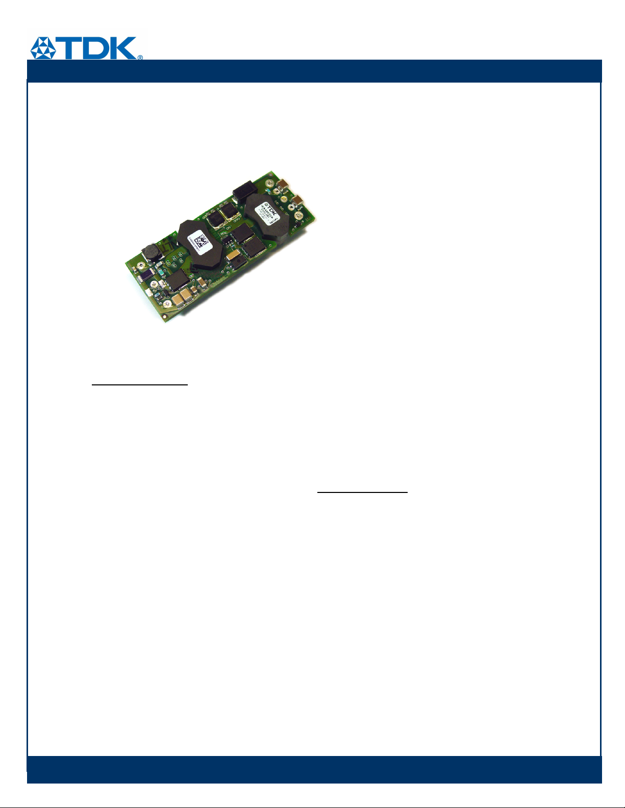
Belleta® iEA Series DC/DC Power Modules
The Belleta Series offers an industry standard
eighth brick power module with true useable
power. Thanks to its low component count and
single-board open-frame design, it provides both
better electrical and thermal performance, and
lower cost than many other suppliers’ eighth brick
product offerings. Belleta® modules are perfect
for both next generation planning and cost
reduction design environments
• UL 60950 (US and Canada), VDE
0805, CB scheme (IEC950), CE
Mark (EN60950)
• ISO Certified manufacturing
facilities
• Patented Design
Optional Features:
• Remote on/off (negative logic)
• Latching output over-voltage
protection
• Short Thru-hole pins 2.79 mm
(0.110”)
• Long Thru-hole pins 5.08 mm
(0.200”)
48V Input, 25A Output
Eighth Brick
©2004 TDK Innoveta® Inc.
iEAFullDatasheet 032707 3/29/2007 Revision 2.0
1/41
Page 2
Data Sheet: Belleta® iEA Series –Single Output Eighth Brick
℡ (877) 498
-
0099
http://www.tdkinnoveta.com/
Ordering information:
Product
Identifier
TDK Innoveta
Option Table:
Feature
Product Offering:
iEA48007A120V 36-75V 12V 6.5A 78W 91%
iEA48015A050V 36-75V 5V 15A 75W 90%
iEA48020A033V 36-75V 3.3V 20A 66W 90%
iEA48025A025V 36-75V 2.5V 25A 62.5W 86%
iEA48025A018V 36-75V 1.8V 25A 45W 83%
iEA48025A015V 36-75V 1.5V 25A 37.5W 81%
iEA48025A012V 36-75V 1.2V 25A 30W 78%
Package
Size
i E A 48 020 A 033 V -
Eighthbrick
Platform
Belleta 36-75V
Input
Voltage
Output
Current/
Power
015 –15A
020 – 20A
025 – 25A
Output
Units
Amps
Main
Output
Voltage
120 – 12V
050 – 5V
033 – 3.3V
025 – 2.5V
018 – 1.8V
015 – 1.5V
012 – 1.2V
# of
Outputs
Single
Safety
Class
0 00
Positive Logic
Set
00 X X
01 X X
02 X X
03 X X
04 X X
05 X X
11 X X X
15 X X X
On/Off
Negative Logic
On/Off
0.110” Pin
Length
0.200” Pin
Length
0.145” Pin
Length
Latching
Code Input Voltage Output Voltage
Output
Current
Maximum
Output Power
00 – Standard
OVP
Feature Set
Efficiency
3320 Matrix Drive, Suite 100
Richardson, TX 75082
Phone (877) 498-0099 Toll Free
(469) 916-4747
Fax (877) 498-0143 Toll Free
(214) 239-3101
support@tdkinnoveta.com
©2004 TDK Innoveta® Inc.
iEAFullDatasheet 032707 3/29/2007 Revision 2.0
2/41
Page 3
℡ (877) 498
-
0099
6
4
Data Sheet: Belleta® iEA Series –Single Output Eighth Brick
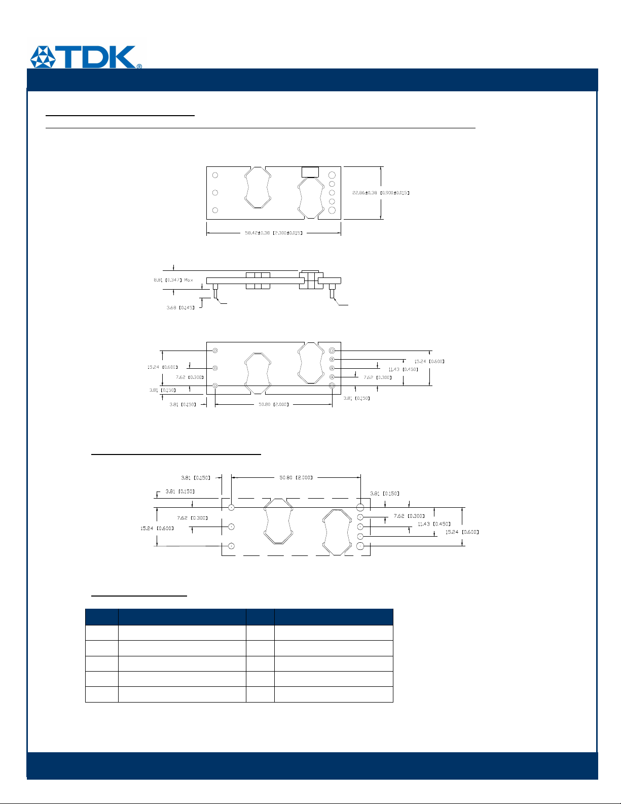
Mechanical Specification:
Dimensions are in mm [in]. Unless otherwise specified tolerances are: x.x ± 0.5 [0.02], x.xx and x.xxx ± 0.25 [0.010].
1.02 [0.040] DIA Pin
2.03 [0.080] DIA Stand-Offs
6 Pins
1.57 [0.062] DIA Pin
2.59 [0.102] DIA Stand-Offs
2 Pins
Recommended Hole Pattern: (top view)
1
2
3
8
7
5
Pin Assignment:
PIN FUNCTION PIN FUNCTION
1 Vin(+) 4 Vo(-)
2 On/Off 5 Sense(-)
3 Vin(-) 6 Trim
7 Sense(+)
8 Vo(+)
Pin base material is brass with tin plating; the maximum module weight is 30.4g (1.07 oz).
©2004 TDK Innoveta® Inc.
iEAFullDatasheet 032707 3/29/2007 Revision 2.0
3/41
Page 4
℡ (877) 498
-
0099
Data Sheet: Belleta® iEA Series –Single Output Eighth Brick
Absolute Maximum Ratings:
Stress in excess of Absolute Maximum Ratings may cause permanent damage to the device.
Characteristic Min Max Unit Notes & Conditions
Continuous Input Voltage -0.5 80 Vdc
Transient Input Voltage --- 100 Vdc 100mS max.
Isolation Voltage --- 1500 Vdc
Storage Temperature -55 125 ˚C
Operating Temperature Range (Tc)
Measured at the location specified in the thermal
-40 125 ˚C
measurement figure. Maximum temperature varies
with model number, output current, and module
orientation – see curve in thermal performance
section of the data sheet.
Input Characteristics:
Unless otherwise specified, specifications apply over all Rated Input Voltage, Resistive Load, and Temperature conditions.
Characteristic Min Typ Max Unit Notes & Conditions
Operating Input Voltage 36 48 75 Vdc
Maximum Input Current --- --- 4 A Vin = 0 to Vin,max
Turn-on Voltage --- 33 --- Vdc
Turn-off Voltage 26 30 --- Vdc
Hysteresis 0.5 3 --- Vdc
Startup Delay Time from application of input
voltage
Startup Delay Time from on/off --- 35 --- mS Vo = 0 to 0.1*Vo,nom; Vin = Vi,nom,
Output Voltage Rise Time --- 50 --- mS Io=Io,max,Tc=25˚C, Vo=0.1 to 0.9*Vo,nom
Inrush Transient --- --- 0.2 A2s
Input Reflected Ripple --- 15 --- mApp See input/output ripple and noise
Input Ripple Rejection --- 55 --- dB @120Hz
Caution: The power modules are not internally fused. An external input line normal blow fuse with a
maximum value of 10A is required, see the Safety Considerations section of the data sheet.
--- 35 --- mS Vo = 0 to 0.1*Vo,nom; on/off =on,
Io=Io,max, Tc=25˚C
Io=Io,max,Tc=25˚C
measurements figure; BW = 20 MHz
©2004 TDK Innoveta® Inc.
iEAFullDatasheet 032707 3/29/2007 Revision 2.0
4/41
Page 5

Data Sheet: Belleta® iEA Series –Single Output Eighth Brick
℡ (877) 498
-
0099
Electrical Data:
iEA48007A120V-000 through -015: 12V, 6.5A Output
Characteristic Min Typ Max Unit Notes & Conditions
Output Voltage Initial Setpoint 11.64 12 12.36 Vdc Vin=Vin,nom; Io=Io,max; Tc = 25˚C
Output Voltage Tolerance 11.58 12 12.42 Vdc
Efficiency --- 90.5 --- % Vin=Vin,nom; Io=Io,max; Tc = 25˚C
Line Regulation --- 10 24 mV Vin=Vin,min to Vin,max
Load Regulation --- 10 24 mV Io=Io,min to Io,max
Temperature Regulation --- 60 240 mV Tc=Tc,min to Tc,max
Output Current 0.5 --- 6.5 A
Output Current Limiting Threshold --- 8.5 --- A Vo = 0.9*Vo,nom, Tc<Tc,max
Short Circuit Current --- 12 --- A Vo = 0.25V, Tc = 25˚C
Over all rated input voltage, load, and
temperature conditions to end of life
At loads less than Io,min the module will
continue to regulate the output voltage, but
the output ripple may increase
--- 80 200
Output Ripple and Noise Voltage
--- 26 --- mVrms
Output Voltage Adjustment Range 90 --- 110 %Vo,nom
Output Voltage Sense Range --- --- 10 %Vo,nom
Dynamic Response:
Recovery Time
Transient Voltage
Output Voltage Overshoot during startup --- --- 5 % Vin=Vin,nom; Io=Io,max,Tc=25˚C
Switching Frequency --- 400 --- kHz Fixed
Output Over Voltage Protection 13.6 --- 15.7 V
External Load Capacitance 0 --- 2000& uF
Isolation Capacitance --- 1000 --- pF
Isolation Resistance 10 --- --- MΩ
Vref 1.225 V Required for trim calculation
& Contact TDK Innoveta for applications that require additional capacitance or very low esr
---
---
60
220
---
---
mVpp
uS
mV
Measured across one 1.0 uF ceramic
capacitor and a 10uF tantalum capacitor –
see input/output ripple measurement figure;
BW = 20MHz
di/dt = 0.1A/uS, Vin=Vin,nom; load step
from 50% to 75% of Io,max
©2004 TDK Innoveta® Inc.
iEAFullDatasheet 032707 3/29/2007 Revision 2.0
5/41
Page 6
℡ (877) 498
-
0099
Data Sheet: Belleta® iEA Series –Single Output Eighth Brick
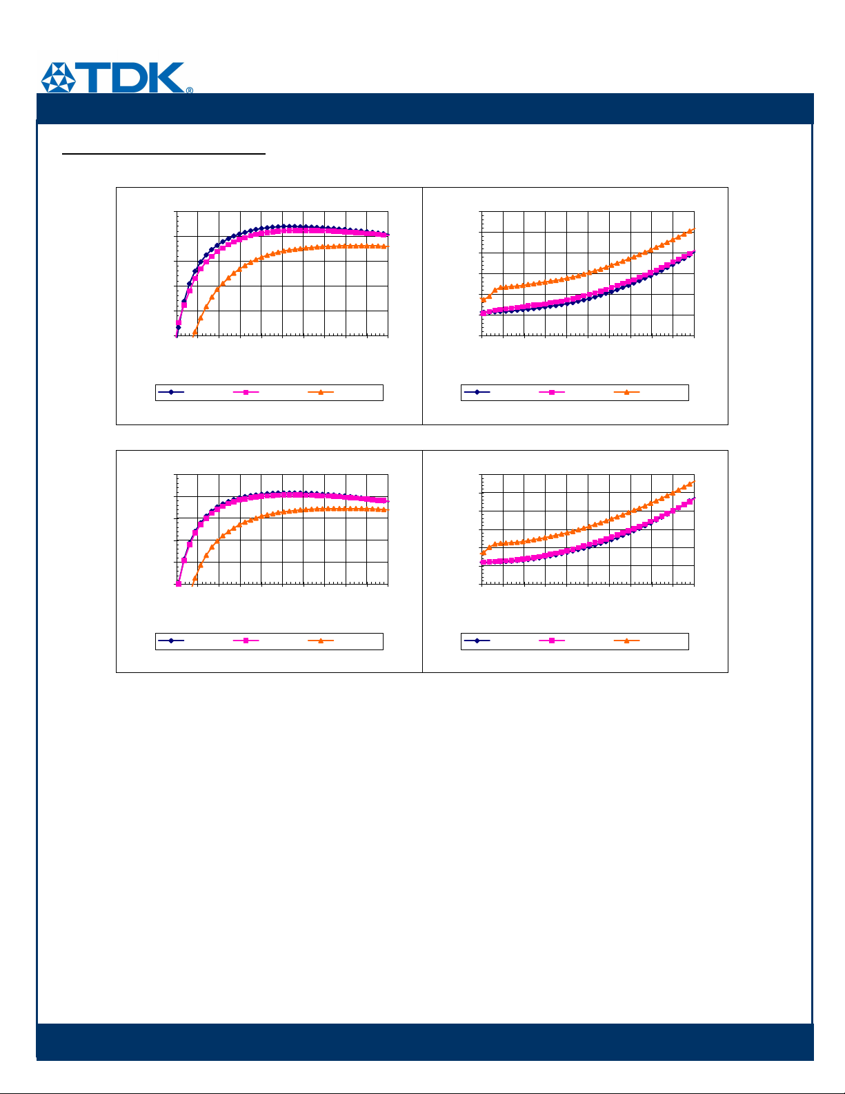
Electrical Characteristics:
iEA48007A120V-000 through -015: 12V, 6.5A Output
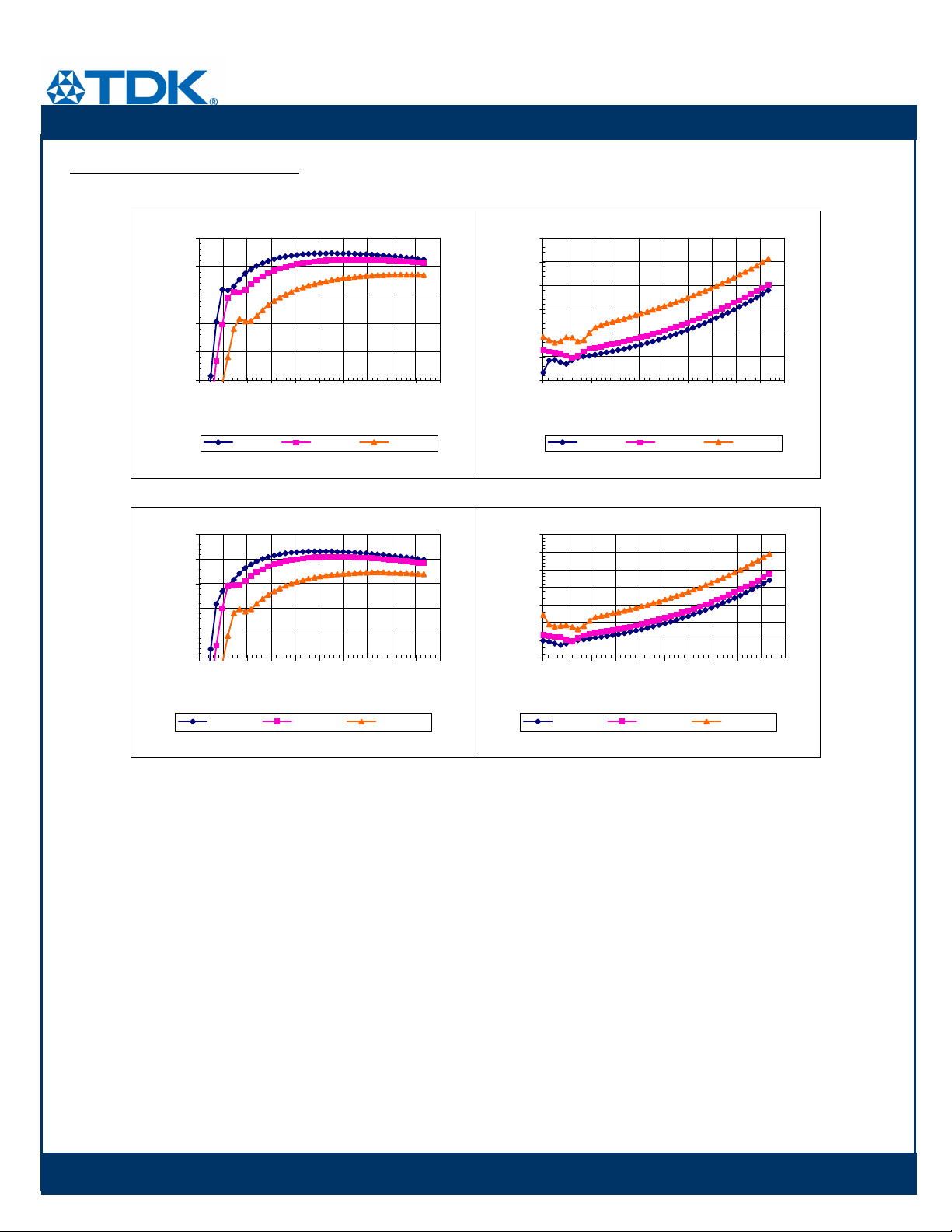
95
90
(%)
η
η
η
η
85
80
Efficiency,
75
70
0 0.7 1.4 2.1 2.8 3.5 4.2 4.9 5.6 6.3 7
Output Current (A)
Vin = 36V Vin = 48V Vin = 75V
iEA48007A120V-000 Typical Efficiency vs. Input
Voltage at Ta=25 degrees.
95
90
(%)
η
η
η
η
85
80
75
Efficiency,
70
0 0.7 1.4 2.1 2.8 3.5 4.2 4.9 5.6 6.3 7
Output Current (A)
12
10
8
6
4
2
Power Dissipation (W)
0
0 0.7 1.4 2.1 2.8 3.5 4.2 4.9 5.6 6.3 7
Output Current (A)
Vin = 36V Vin = 48V Vin = 75V
iEA48007A120V-000 Typical Power Dissipation vs.
Input Voltage at Ta=25 degrees
14
12
10
8
6
4
2
Power Dissipation (W)
0
0 0.7 1.4 2.1 2.8 3.5 4.2 4.9 5.6 6.3 7
Output Current (A)
Vin = 36V Vin = 48V Vin = 75V
iEA48007A120V-000 Typical Efficiency vs. Input
Voltage at Ta=85 degrees.
©2004 TDK Innoveta® Inc.
iEAFullDatasheet 032707 3/29/2007 Revision 2.0
Vin = 36V Vin = 48V Vin = 75V
iEA48007A120V-000 Typical Power Dissipation vs.
Input Voltage at Ta=85 degrees
6/41
Page 7
Data Sheet: Belleta® iEA Series –Single Output Eighth Brick
℡ (877) 498
-
0099
1.2255×
5
Electrical Characteristics (continued):
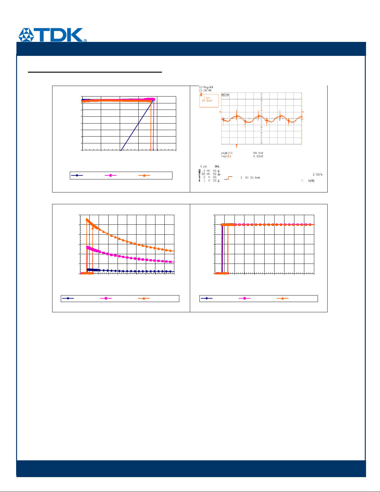
iEA48007A120V-000 through -015: 12V, 6.5A Output
12.34
12.24
12.14
12.04
11.94
11.84
11.74
Output Voltage (V)
11.64
0 0.7 1.4 2.1 2.8 3.5 4.2 4.9 5.6 6.3 7
Output Current (A)
Vin = 36V Vin = 48V Vin = 75V
iEA48007A120V-000 Typical Output Voltage vs. Load
Current at Ta = 25 degrees
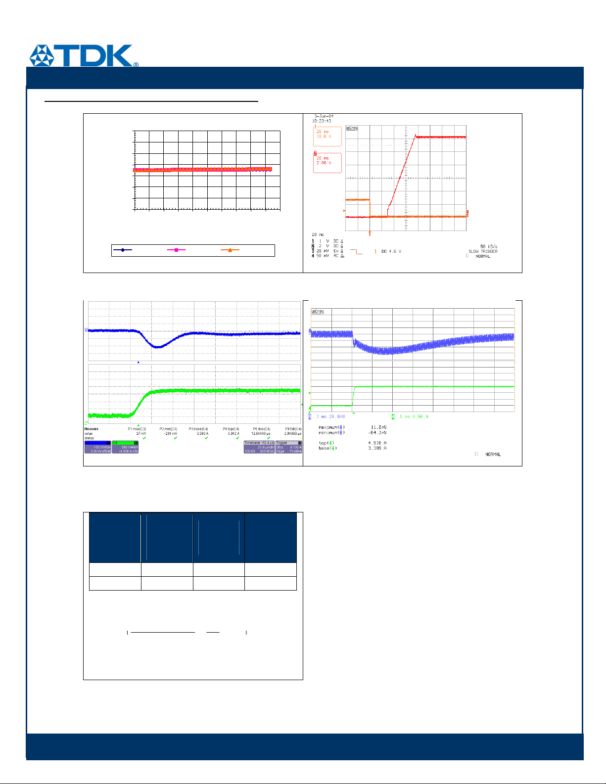
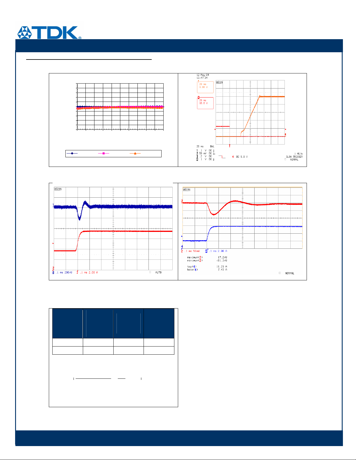
iEA48007A120V-001 Typical startup characteristic from
on/off at full load. Ch 1 - on/off signal, Ch 2 – output
voltage
iEA48007A120V-000 Typical Output voltage response
to load step from 50% to 75% of full load with output
current slew rate of 0.1A/uS.
5.1 12× 100 5+( )⋅
Trim
Down
Resistor
(Kohm)
%
Change
of Vout
510
− 10.2−
%
Change
of Vout
-5% 91.8K +5% 937K
-10% 40.8K +10% 488K
e.g. trim up 5%
Rup
iEA48007A120V-000 Calculated resistor values for
output voltage adjustment
©2004 TDK Innoveta® Inc.
iEAFullDatasheet 032707 3/29/2007 Revision 2.0
Trim Up
Resistor
(Kohm)
K⋅:=
iEA48007A120V-000 Typical Output voltage response
to load step from 50% to 75% of full load with output
current slew rate of 0.1A/uS and 2200uF external load.
7/41
Page 8
Data Sheet: Belleta® iEA Series –Single Output Eighth Brick
℡ (877) 498
-
0099
Electrical Characteristics (continued):
iEA48007A120V-000 through -015: 12V, 6.5A Output
12.5
12
11.5
11
Output Voltage (V)
10.5
10
0 2 4 6 8 10 12
Output Current (A)
Vin = 36V Vin = 48V Vin = 75V
iEA48007A120V-000 Typical Output Current Limit
Characteristics vs. Input Voltage at Ta=25 degrees.
3.5
3
2.5
2
1.5
1
Input Current (A)
0.5
0
27 32 37 41 46 51 56 61 65 7 0 75
Input Voltage (V)
Io_min = 0A Io_mid = 3.3A Io_max = 6.5A
iEA48007A120V-000 Typical Input Current vs. Input
Voltage Characteristics
iEA48007A120V-000 Typical Output Ripple at nominal
input voltage and full load at Ta=25 degrees
14
12
10
8
6
4
Output Voltage (V)
2
0
27 32 37 41 46 51 56 61 65 70 75
Input Voltage (V)
Io_min = 0A Io_mid = 3.3A Io_max = 6.5A
iEA48007A120V-000 Typical Output Voltage vs. Input
Voltage Characteristics
©2004 TDK Innoveta® Inc.
iEAFullDatasheet 032707 3/29/2007 Revision 2.0
8/41
Page 9
Data Sheet: Belleta® iEA Series –Single Output Eighth Brick
℡ (877) 498
-
0099
Thermal Performance:
iEA48007A120V-000 through -015: 12V, 6.5A Output
7
6
5
4
3
2
1
0
25 45 65 85 105 125
NC
0.5 m/s (10 0 LFM)
1.0 m/ s (200 LFM)
2.0 m/s (400 LFM)
3.0 m/s (600 LFM)
Tc, Thermal Limi t
T emp er at ure ( oC )
7
6
5
4
3
2
Output Current (A)
1
0
25 45 65 85 105 125
NC
0.5 m/s (100 LFM)
1.0 m/s (200 LFM)
2.0 m/s (400 LFM)
3.0 m/s (600 LFM)
Tc, Thermal Limit
Temperature (oC)
iEA48007A120V-000 maximum output current vs. ambient
temperature at nominal input voltage for airflow rates natural
convection (60lfm) to 600lfm with airflow from pin 3 to pin 1.
iEA48007A120V-000 maximum output current vs.ambient
temperature at nominal input voltage for airflow rates natural
convection (60lfm) to 600lfm with airflow from pin 1 to pin 3.
Best orientation
airflow
Thermal measurement
location on PWB Cu
iEA48007A120V-000 thermal measurement location –
top view
Both the thermal curves provided and the example given above are based upon measurements made in TDK Innoveta’s
experimental test setup that is described in the Thermal Management section. Due to the large number of variables in
system design, TDK Innoveta recommends that the user verify the module’s thermal performance in the end application.
The critical component should be thermo coupled and monitored, and should not exceed the temperature limit specified in
the derating curve above. It is critical that the thermocouple be mounted in a manner that gives direct thermal contact or
significant measurement errors may result. TDK Innoveta can provide modules with a thermocouple pre-mounted to the
critical component for system verification tests.
©2004 TDK Innoveta® Inc.
iEAFullDatasheet 032707 3/29/2007 Revision 2.0
9/41
Page 10

Data Sheet: Belleta® iEA Series –Single Output Eighth Brick
℡ (877) 498
-
0099
Electrical Data:
iEA48015A050V-000 through -015: 5V, 15A Output
Characteristic Min Typ Max Unit Notes & Conditions
Output Voltage Initial Setpoint 4.92 5 5.08 Vdc Vin=Vin,nom; Io=Io,max; Tc = 25˚C
Output Voltage Tolerance 4.85 5 5.15 Vdc
Efficiency --- 90 --- % Vin=Vin,nom; Io=Io,max; Tc = 25˚C
Line Regulation --- 2 10 mV Vin=Vin,min to Vin,max
Load Regulation --- 1 10 mV Io=Io,min to Io,max
Temperature Regulation --- 30 75 mV Tc=Tc,min to Tc,max
Output Current 1 --- 15 A
Output Current Limiting Threshold --- 20 --- A Vo = 0.9*Vo,nom, Tc<Tc,max
Short Circuit Current --- 14 --- A Vo = 0.25V, Tc = 25˚C
Over all rated input voltage, load, and
temperature conditions to end of life
At loads less than Io,min the module will
continue to regulate the output voltage, but
the output ripple may increase
--- 55 125
Output Ripple and Noise Voltage
--- 7 --- mVrms
Output Voltage Adjustment Range 90 --- 110 %Vo,nom
Output Voltage Sense Range --- --- 10 %Vo,nom
Dynamic Response:
Recovery Time
Transient Voltage
Output Voltage Overshoot during startup --- --- 250 mV Vin=Vin,nom; Io=Io,max,Tc=25˚C
Switching Frequency --- 400 --- kHz Fixed
Output Over Voltage Protection 5.7 --- 6.7 V
External Load Capacitance 0 --- 5000& uF
Isolation Capacitance --- 1000 --- pF
Isolation Resistance 10 --- --- MΩ
Vref 1.225 V Required for trim calculation
& Contact TDK Innoveta for applications that require additional capacitance or very low esr
---
---
100
200
---
---
mVpp
uS
mV
Measured across one 0.1 uF ceramic
capacitor and a 22uF ceramic capacitor –
see input/output ripple measurement figure;
BW = 20MHz
di/dt = 0.1A/uS, Vin=Vin,nom; load step
from 50% to 75% of Io,max
©2004 TDK Innoveta® Inc.
iEAFullDatasheet 032707 3/29/2007 Revision 2.0
10/41
Page 11
℡ (877) 498
-
0099
Data Sheet: Belleta® iEA Series –Single Output Eighth Brick
Electrical Characteristics:
iEA48015A050V-000 through -015: 5V, 15A Output
95
90
(%)
η
η
η
η
85
80
Efficiency,
75
70
1 2.4 3 .8 5.2 6.6 8 9.4 10.8 12.2 13.6 15
Output Current (A)
Vin = 36V Vin = 48V Vin = 75V
iEA48015A050V-000 Typical Efficiency vs. Input
Voltage at Ta=25 degrees.
95
90
(%)
η
η
η
η
85
80
75
Efficiency,
70
1 2.4 3 .8 5.2 6.6 8 9.4 10.8 12.2 13.6 15
Output Current (A)
12
10
8
6
4
2
Power Dissipation (W)
0
1 2.4 3 .8 5.2 6.6 8 9.4 10.8 12.2 13.6 15
Output Current (A)
Vin = 36V Vin = 48V Vin = 75V
iEA48015A050V-000 Typical Power Dissipation vs.
Input Voltage at Ta=25 degrees
12
10
8
6
4
2
Power Dissipation (W)
0
1 2.4 3 .8 5.2 6.6 8 9.4 10.8 12.2 13.6 15
Output Current (A)
Vin = 36V Vin = 48V Vin = 75V
iEA48015A050V-000 Typical Efficiency vs. Input
Voltage at Ta=85 degrees.
©2004 TDK Innoveta® Inc.
iEAFullDatasheet 032707 3/29/2007 Revision 2.0
Vin = 36V Vin = 48V Vin = 75V
iEA48015A050V-000 Typical Power Dissipation vs.
Input Voltage at Ta=85 degrees
11/41
Page 12
℡ (877) 498
-
0099
1.2255×
5
Data Sheet: Belleta® iEA Series –Single Output Eighth Brick
Electrical Characteristics (continued):
iEA48015A050V-000 through -015: 5V, 15A Output
5.05
5.04
5.03
5.02
5.01
5
4.99
4.98
4.97
Output Voltage (V)
4.96
4.95
1 2.4 3.8 5.2 6.6 8 9.4 10.8 12.2 13.6 15
Output Current (A)
Vin = 36V Vin = 48V Vin = 75V
iEA48015A050V-000 Typical Output Voltage vs. Load
Current at Ta = 25 degrees
iEA48015A050V-000 Typical Output voltage response
to load step from 50% to 75% of full load with output
current slew rate of 0.1A/uS.
5.1 5× 100 5+( )⋅
Trim
Down
Resistor
(Kohm)
%
Change
of Vout
510
− 10.2−
%
Change
of Vout
-5% 91.8K +5% 325K
-10% 40.8K +10% 168K
e.g. trim up 5%
Rup
Trim Up
Resistor
(Kohm)
K⋅:=
iEA48015A050V-001 Typical startup characteristic from
on/off at full load. Ch4 - on/off signal, Ch 1 – output
voltage
iEA48015A050V-000 Typical Output voltage response
to load step from 50% to 75% of full load with output
current slew rate of 0.1A/uS and 5000uF load.
iEA48015A050V-000 Calculated resistor values for
output voltage adjustment
©2004 TDK Innoveta® Inc.
iEAFullDatasheet 032707 3/29/2007 Revision 2.0
12/41
Page 13
Data Sheet: Belleta® iEA Series –Single Output Eighth Brick
℡ (877) 498
-
0099
Electrical Characteristics (continued):
iEA48015A050V-000 through -015: 5V, 15A Output
5.01
4.99
4.97
4.95
4.93
4.91
4.89
Output Voltage (V)
4.87
4.85
1 6 11 16 21 26
Output Current (A)
Vin = 36V Vin = 48V Vin = 75V
iEA48015A050V-000 Typical Output Current Limit
Characteristics vs. Input Voltage at Ta=25 degrees.
iEA48015A050V-000 Typical Output Ripple at nominal
input voltage and full load at Ta=25 degrees
3
2.5
2
1.5
1
Input Current (A)
0.5
0
27 32 37 41 46 51 56 61 65 7 0 75
Input Voltage (V)
Io_min = 0 .8A Io_mid = 7.5A Io_max = 15.1A
iEA48015A050V-000 Typical Input Current vs. Input
Voltage Characteristics
6
5
4
3
2
Output Voltage (V)
1
0
27 32 37 41 46 51 56 61 65 70 75
Input Voltage (V)
Io_min = 0.8A Io_mid = 7.5A Io_max = 15.1A
iEA48015A050V-000 Typical Output Voltage vs. Input
Voltage Characteristics
©2004 TDK Innoveta® Inc.
iEAFullDatasheet 032707 3/29/2007 Revision 2.0
13/41
Page 14

Data Sheet: Belleta® iEA Series –Single Output Eighth Brick
℡ (877) 498
-
0099
Output Current (A)
Thermal Performance:
iEA48015A050V-000 through -015: 5V, 15A Output
16
14
12
10
8
6
4
2
0
25 45 65 85 105 1 25
NC
0.5 m/s (100 LFM)
1.0 m/s (200 LFM)
2.0 m/s (400 LFM)
3.0 m/s (600 LFM)
Tc, Thermal Limit
Temperature (oC)
iEA48015A050V-000 maximum output current vs. ambient
temperature at nominal input voltage for airflow rates natural
convection (60lfm) to 600lfm with airflow from pin 3 to pin 1.
Best orientation
airflow
Thermal measurement
location on PWB Cu
iEA48015A050V-000 thermal measurement location –
top view
Both the thermal curves provided and the example given above are based upon measurements made in TDK Innoveta’s
experimental test setup that is described in the Thermal Management section. Due to the large number of variables in
system design, TDK Innoveta recommends that the user verify the module’s thermal performance in the end application.
The critical component should be thermo coupled and monitored, and should not exceed the temperature limit specified in
the derating curve above. It is critical that the thermocouple be mounted in a manner that gives direct thermal contact or
significant measurement errors may result. TDK Innoveta can provide modules with a thermocouple pre-mounted to the
critical component for system verification tests.
©2004 TDK Innoveta® Inc.
iEAFullDatasheet 032707 3/29/2007 Revision 2.0
14/41
Page 15

Data Sheet: Belleta® iEA Series –Single Output Eighth Brick
℡ (877) 498
-
0099
Electrical Data:
iEA48020A033V-000 through -015: 3.3V, 20A Output
Characteristic Min Typ Max Unit Notes & Conditions
Output Voltage Initial Setpoint 3.25 3.3 3.35 Vdc Vin=Vin,nom; Io=Io,max; Tc = 25˚C
Output Voltage Tolerance 3.20 3.3 3.40 Vdc
Efficiency --- 89.5 --- % Vin=Vin,nom; Io=Io,max; Tc = 25˚C
Line Regulation --- 2 7 mV Vin=Vin,min to Vin,max
Load Regulation --- 3 8 mV Io=Io,min to Io,max
Temperature Regulation --- 15 60 mV Tc=Tc,min to Tc,max
Output Current 1.5 --- 20 A
Output Current Limiting Threshold --- 29 --- A Vo = 0.9*Vo,nom, Tc<Tc,max
Short Circuit Current --- 20 --- A Vo = 0.25V, Tc = 25˚C
Over all rated input voltage, load, and
temperature conditions to end of life
At loads less than Io,min the module will
continue to regulate the output voltage, but
the output ripple may increase
--- 35 100
Output Ripple and Noise Voltage
--- 11 --- mVrms
Output Voltage Adjustment Range 90 --- 110 %Vo,nom
Output Voltage Sense Range --- --- 10 %Vo,nom
Dynamic Response:
Recovery Time
Transient Voltage
Output Voltage Overshoot during startup --- --- 165 mV Vin=Vin,nom; Io=Io,max,Tc=25˚C
Switching Frequency --- 400 --- kHz Fixed
Output Over Voltage Protection 3.75 --- 4.4 V
External Load Capacitance 100 --- 5000& uF Recommend TDK part C3225X5R0J107MT
Isolation Capacitance --- 1000 --- pF
Isolation Resistance 10 --- --- MΩ
Vref 1.225 V Required for trim calculation
& Contact TDK Innoveta for applications that require additional capacitance or very low esr
---
---
90
180
---
---
mVpp
uS
mV
Measured across one 1.0 uF ceramic
capacitor and a 10uF tantalum capacitor –
see input/output ripple measurement figure;
BW = 20MHz
The trim range is reduced to 105% when
the input voltage is below 40V.
The sense range is reduced to 5% when the
input voltage is below 40V.
di/dt = 0.1A/uS, Vin=Vin,nom; load step
from 50% to 75% of Io,max
©2004 TDK Innoveta® Inc.
iEAFullDatasheet 032707 3/29/2007 Revision 2.0
15/41
Page 16

℡ (877) 498
-
0099
Data Sheet: Belleta® iEA Series –Single Output Eighth Brick
Electrical Characteristics:
iEA48020A033V-000 through -015: 3.3V, 20A Output
95
90
(%)
η
η
η
η
85
80
Efficiency,
75
70
1 2.9 4.8 6.7 8.6 10.5 12.4 14.3 16.2 18.1 20
Output Current (A)
Vin = 36V Vin = 48V Vin = 75V
iEA48020A033V-000 Typical Efficiency vs. Input
Voltage at Ta=25 degrees.
95
90
(%)
η
η
η
η
85
80
Efficiency,
75
70
1 2.9 4 .8 6.7 8.6 10.5 12.4 14. 3 16.2 18.1 20
Output Current (A)
12
10
8
6
4
2
Power Dissipation (W)
0
1 2.9 4.8 6.7 8.6 10.5 12.4 14.3 16.2 18.1 20
Output Current (A)
Vin = 36V Vin = 48V Vin = 75V
iEA48020A033V-000 Typical Power Dissipation vs.
Input Voltage at Ta=25 degrees
12
10
8
6
4
2
Power Dissipation (W)
0
1 2.9 4 .8 6.7 8.6 10.5 12.4 14.3 16.2 18.1 20
Output Current (A)
Vin = 36V Vin = 48V Vin = 75V
iEA48020A033V-000 Typical Efficiency vs. Input
Voltage at Ta=85 degrees.
©2004 TDK Innoveta® Inc.
iEAFullDatasheet 032707 3/29/2007 Revision 2.0
Vin = 36V Vin = 48V Vin = 75V
iEA48020A033V-000 Typical Power Dissipation vs.
Input Voltage at Ta=85 degrees
16/41
Page 17

Data Sheet: Belleta® iEA Series –Single Output Eighth Brick
℡ (877) 498
-
0099
1.225
5
5
Electrical Characteristics (continued):
iEA48020A033V-000 through -015: 3.3V, 20A Output
3.35
3.33
3.31
3.29
3.27
Output Voltage (V)
3.25
1 2.9 4.8 6.7 8.6 10.5 12.4 14.3 16.2 18.1 20
Output Current (A)
Vin = 36V Vin = 48V Vin = 75V
iEA48020A033V-000 Typical Output Voltage vs. Load
Current at Ta = 25 degrees
iEA48020A033V-001 Typical startup characteristic from
on/off at full load. Ch2 - on/off signal, Ch 1 – output
voltage
iEA48020A033V-000 Typical output voltage response
to load step from 50% to 75% of full load with output
current slew rate of 0.1A/uS.
5.1 3.3× 100 5+( )⋅
Trim
Down
Resistor
(Kohm)
×
%
Change
of Vout
510
− 10.2−
%
Change
of Vout
-5% 91.8K +5% 176.3K
-10% 40.8K +10% 89.9K
e.g. trim up 5%
Rup
iEA48020A033V-000 Calculated resistor values for
output voltage adjustment
©2004 TDK Innoveta® Inc.
iEAFullDatasheet 032707 3/29/2007 Revision 2.0
iEA48020A033V-000 Typical output voltage response
to load step from 50% to 75% of full load with output
current slew rate of 0.1A/uS and 5000uF load.
Trim Up
Resistor
(Kohm)
K⋅:=
17/41
Page 18

Data Sheet: Belleta® iEA Series –Single Output Eighth Brick
℡ (877) 498
-
0099
Electrical Characteristics (continued):
iEA48020A033V-000 through -015: 3.3V, 20A Output
3.32
3.31
3.3
3.29
3.28
3.27
Output Voltage (V)
3.26
3.25
20 22 24 26 28 30 32
Output Current (A)
Vin = 36V Vin = 48V Vin = 75V
iEA48020A033V-000 Typical Output Current Limit
Characteristics vs. Input Voltage at Ta=25 degrees.
iEA48020A033V-000 Typical Output Ripple at nominal
input voltage and full load at Ta=25 degrees
3
2.5
2
1.5
1
Input Current (A)
0.5
0
27 32 37 41 46 51 56 61 65 70 75
Input Voltage (V)
Io_min = 1A Io_mid = 10A Io_max = 20A
iEA48020A033V-000 Typical Input Current vs. Input
Voltage Characteristics
3.5
3
2.5
2
1.5
1
Output Voltage (V)
0.5
0
27 32 37 41 46 51 56 61 65 70 75
Input Voltage (V)
Io_min = 1A Io_mid = 10A Io_max = 20A
iEA48020A033V-000 Typical Output Voltage vs. Input
Voltage Characteristics
©2004 TDK Innoveta® Inc.
iEAFullDatasheet 032707 3/29/2007 Revision 2.0
18/41
Page 19

Data Sheet: Belleta® iEA Series –Single Output Eighth Brick
℡ (877) 498
-
0099
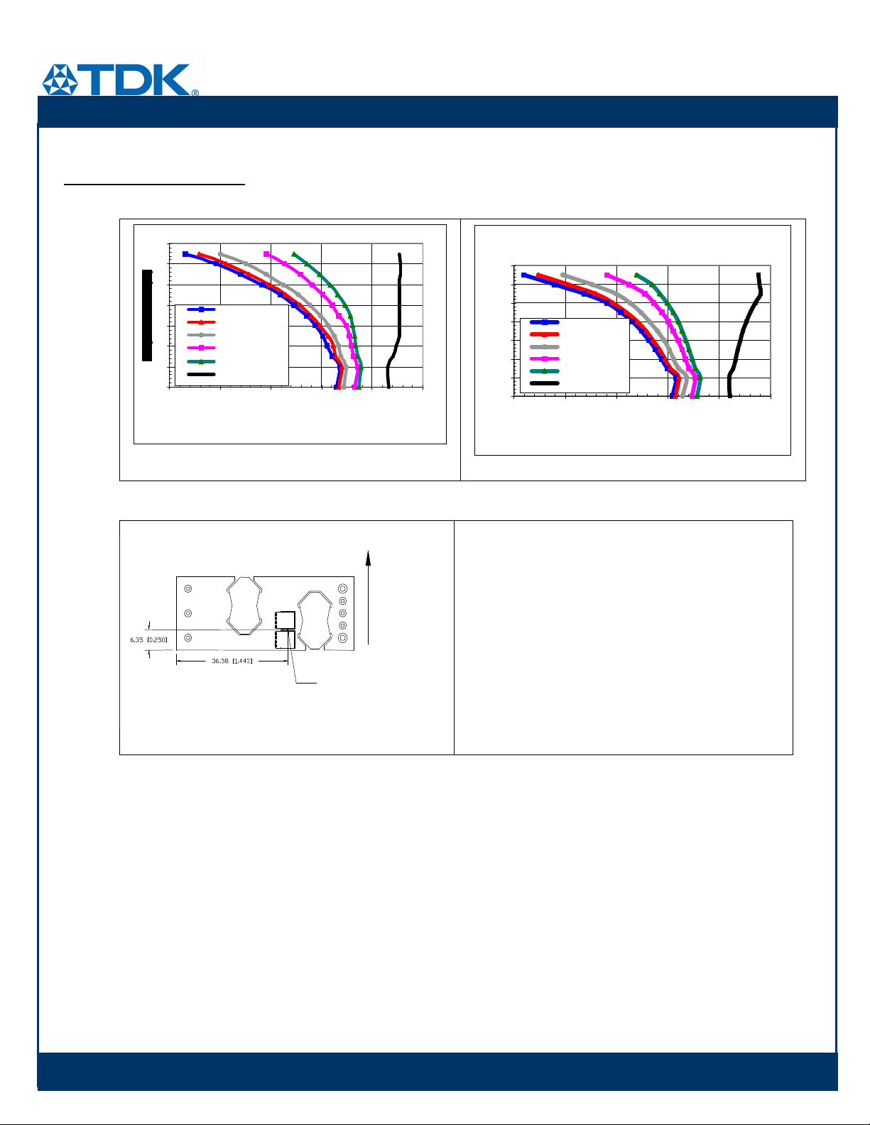
Thermal Performance:
iEA48020A033V-000 through -015: 3.3V, 20A Output
25
20
15
Output Current (A)
10
5
NC
0.5 m/s (100 LFM)
1.0 m/s (200 LFM)
2.0 m/s (400 LFM)
3.0 m/s (600 LFM)
Tc, Thermal Limit
30 40 50 60 70 80 90 100 11 0 120 130
Temperature (C)
iEA48020A033V-000 maximum output current vs. ambient
temperature at nominal input voltage for airflow rates natural
convection (60lfm) to 600lfm with airflow from pin 3 to pin 1.
25
20
15
Output Current (A)
10
5
30 40 50 60 70 80 90 100 110 120 130
NC
0.5 m/s (100 LFM)
1.0 m/s (200 LFM)
2.0 m/s (400 LFM)
3.0 m/s (600 LFM)
Tc, Thermal Limit
Temperature (C)
iEA48020A033V-000 maximum output current vs. ambient
temperature at nominal input voltage for airflow rates natural
convection (60lfm) to 600lfm with airflow from pin 1 to pin 3.
Best orientation
airflow
iEA48020A033V-000 thermal measurement location –
Both the thermal curves provided and the example given above are based upon measurements made in TDK Innoveta’s
experimental test setup that is described in the Thermal Management section. Due to the large number of variables in
system design, TDK Innoveta recommends that the user verify the module’s thermal performance in the end application.
The critical component should be thermo coupled and monitored, and should not exceed the temperature limit specified in
the derating curve above. It is critical that the thermocouple be mounted in a manner that gives direct thermal contact or
significant measurement errors may result. TDK Innoveta can provide modules with a thermocouple pre-mounted to the
critical component for system verification tests.
©2004 TDK Innoveta® Inc.
iEAFullDatasheet 032707 3/29/2007 Revision 2.0
Thermal measurement
location on PWB Cu
top view
19/41
Page 20

Data Sheet: Belleta® iEA Series –Single Output Eighth Brick
℡ (877) 498
-
0099
Electrical Data:
iEA48025A025V-000 through -015: 2.5V, 25A Output
Characteristic Min Typ Max Unit Notes & Conditions
Output Voltage Initial Setpoint 2.46 2.5 2.54 Vdc Vin=Vin,nom; Io=Io,max; Tc = 25˚C
Output Voltage Tolerance 2.42 2.5 2.58 Vdc
Efficiency --- 85.5 --- % Vin=Vin,nom; Io=Io,max; Tc = 25˚C
Line Regulation --- 1 5 mV Vin=Vin,min to Vin,max
Load Regulation --- 1 7 mV Io=Io,min to Io,max
Temperature Regulation --- 10 50 mV Tc=Tc,min to Tc,max
Output Current 2.0 --- 25 A
Output Current Limiting Threshold --- 31 --- A Vo = 0.9*Vo,nom, Tc<Tc,max
Short Circuit Current --- 20 --- A Vo = 0.25V, Tc = 25˚C
Over all rated input voltage, load, and
temperature conditions to end of life
At loads less than Io,min the module will
continue to regulate the output voltage, but
the output ripple may increase
--- 35 100
Output Ripple and Noise Voltage
--- 11 --- mVrms
Output Voltage Adjustment Range 90 --- 110 %Vo,nom
Output Voltage Sense Range --- --- 10 %Vo,nom
Dynamic Response:
Recovery Time
Transient Voltage
Output Voltage Overshoot during startup --- --- 165 mV Vin=Vin,nom; Io=Io,max,Tc=25˚C
Switching Frequency --- 400 --- kHz Fixed
Output Over Voltage Protection 2.7 --- 3.5 V
External Load Capacitance 0 --- 5000& uF
Isolation Capacitance --- 1000 --- pF
Isolation Resistance 10 --- --- MΩ
Vref 1.225 V Required for trim calculation
& Contact TDK Innoveta for applications that require additional capacitance or very low esr
---
---
100*
200*
---
---
mVpp
uS
mV
Measured across one 1.0 uF ceramic
capacitor and a 10uF tantalum capacitor –
see input/output ripple measurement figure;
BW = 20MHz
di/dt = 0.1A/uS, Vin=Vin,nom; load step
from 50% to 75% of Io,max
©2004 TDK Innoveta® Inc.
iEAFullDatasheet 032707 3/29/2007 Revision 2.0
20/41
Page 21

℡ (877) 498
-
0099
Data Sheet: Belleta® iEA Series –Single Output Eighth Brick
Electrical Characteristics:
iEA48025A025V-000 through -015: 2.5V, 25A Output
95
90
(%)
η
η
η
η
85
80
Efficiency,
75
70
0 2.51 5.02 7.53 10 12.6 15 .1 17.6 20.1 22.6 25.1
Output Current (A)
Vin = 36V Vin = 48V Vin = 75V
iEA48025A025V-000 Typical Efficiency vs. Input
Voltage at Ta=25 degrees.
2.54
2.53
2.52
2.51
2.5
2.49
2.48
Output Voltage (V)
2.47
2.46
0 2.5 5 7.5 10 1 2.5 15 17.5 20 22.5 25
Output Current (A)
14
12
10
8
6
4
2
Power Dissipation (W)
0
0 2.51 5.02 7.53 10 12.6 15.1 17.6 20.1 22.6 25.1
Output Current (A)
Vin = 36V Vin = 48V Vin = 75V
iEA48025A025V-000 Typical Power Dissipation vs.
Input Voltage at Ta=25 degrees
Vin = 36V Vin = 48V Vin = 75V
iEA48025A025V-000 Typical Output Voltage vs. Load
Current at Ta = 25 degrees
iEA48025A025V-000 Typical startup characteristic
from input voltage application at full load. Ch3 - input
voltage, Ch 1 – output voltage
©2004 TDK Innoveta® Inc.
iEAFullDatasheet 032707 3/29/2007 Revision 2.0
iEA48025A025V-001 Typical startup characteristic from
on/off at full load. Ch3 - on/off signal, Ch 1 – output
voltage
2.55
2.5
2.45
2.4
2.35
Output Voltage (V)
2.3
15 20 25 30 35
Output Current (A)
Vin = 36V Vin = 48V Vin = 75V
iEA48025A025V-000 Typical Output Current Limit
Characteristics vs. Input Voltage at Ta=25 degrees.
21/41
Page 22

Data Sheet: Belleta® iEA Series –Single Output Eighth Brick
℡ (877) 498
-
0099
1.2255×
5
Electrical Characteristics (continued):
iEA48025A025V-000 through -015: 2.5V, 25A Output
3
2.5
2
1.5
1
Input Current (A)
0.5
0
27 31.8 36.6 41.4 46.2 5 1 55.8 60.6 65.4 70.2 75
Input Voltage (V)
Io_min = 0A Io_mid = 12.6A Io_max = 25.2A
iEA48025A025V-000 Typical Input Current vs. Input
Voltage Characteristics
5.1 2.5× 100 5+( )⋅
Trim
Down
Resistor
(Kohm)
%
Change
of Vout
510
− 10.2−
Trim Up
Resistor
(Kohm)
K⋅:=
%
Change
of Vout
-5% 91.8K +5% 106K
-10% 40.8K +10% 53.3K
e.g. trim up 5%
Rup
3
2.5
2
1.5
1
0.5
Output Voltage (V)
0
27 32 37 4 1 46 51 56 61 65 7 0 75
Input Voltage (V)
Io_min = 0A Io_mid = 12.6A
Io_max = 25.2A
iEA48025A025V-000 Typical Output Voltage vs. Input
Voltage Characteristics
iEA48025A025V-000 Calculated resistor values for
output voltage adjustment
©2004 TDK Innoveta® Inc.
iEAFullDatasheet 032707 3/29/2007 Revision 2.0
22/41
Page 23

Data Sheet: Belleta® iEA Series –Single Output Eighth Brick
℡ (877) 498
-
0099
Thermal Performance:
iEA48025A025V-000 through -015: 2.5V, 25A Output
30
25
20
15
10
Output Current (A)
5
0
25 45 65 85 105 125
Temperature (oC)
NC 0.5 m /s (100 LFM)
1.0 m/s (200 LFM) 2.0 m/s (400 LFM)
3.0 m/s (600 LFM) Tc, Thermal Limit
iEA48025A025V-000 maximum output current vs. ambient
temperature at nominal input voltage for airflow rates natural
convection (60lfm) to 600lfm with airflow from pin 3 to pin 1.
Best orientation
airflow
Thermal measurement
location on PWB Cu
iEA48025A025V-000 thermal measurement location –
top view
Both the thermal curves provided and the example given above are based upon measurements made in TDK Innoveta’s
experimental test setup that is described in the Thermal Management section. Due to the large number of variables in
system design, TDK Innoveta recommends that the user verify the module’s thermal performance in the end application.
The critical component should be thermo coupled and monitored, and should not exceed the temperature limit specified in
the derating curve above. It is critical that the thermocouple be mounted in a manner that gives direct thermal contact or
significant measurement errors may result. TDK Innoveta can provide modules with a thermocouple pre-mounted to the
critical component for system verification tests.
©2004 TDK Innoveta® Inc.
iEAFullDatasheet 032707 3/29/2007 Revision 2.0
23/41
Page 24

Data Sheet: Belleta® iEA Series –Single Output Eighth Brick
℡ (877) 498
-
0099
Electrical Data:
iEA48025A018V-000 through -015: 1.8V, 25A Output
Characteristic Min Typ Max Unit Notes & Conditions
Output Voltage Initial Setpoint 1.77 1.8 1.83 Vdc Vin=Vin,nom; Io=Io,max; Tc = 25˚C
Output Voltage Tolerance 1.74 1.8 1.86 Vdc
Efficiency --- 82.5 --- % Vin=Vin,nom; Io=Io,max; Tc = 25˚C
Line Regulation --- 1 5 mV Vin=Vin,min to Vin,max
Load Regulation --- 1 7 mV Io=Io,min to Io,max
Temperature Regulation --- 10 50 mV Tc=Tc,min to Tc,max
Output Current 2.0 --- 25 A
Output Current Limiting Threshold --- 35 --- A Vo = 0.9*Vo,nom, Tc<Tc,max
Short Circuit Current --- 20 --- A Vo = 0.25V, Tc = 25˚C
Over all rated input voltage, load, and
temperature conditions to end of life
At loads less than Io,min the module will
continue to regulate the output voltage, but
the output ripple may increase
--- 35 100
Output Ripple and Noise Voltage
--- 8 --- mVrms
Output Voltage Adjustment Range 90 --- 110 %Vo,nom
Output Voltage Sense Range --- --- 10 %Vo,nom
Dynamic Response:
Recovery Time
Transient Voltage
Output Voltage Overshoot during startup --- --- 165 mV Vin=Vin,nom; Io=Io,max,Tc=25˚C
Switching Frequency --- 400 --- kHz Fixed
Output Over Voltage Protection 2.12 --- 2.58 V
External Load Capacitance 0 --- 5000& uF
Isolation Capacitance --- 1000 --- pF
Isolation Resistance 10 --- --- MΩ
Vref 1.225 V Required for trim calculation
& Contact TDK Innoveta for applications that require additional capacitance or very low esr
---
---
120
130
---
---
mVpp
uS
mV
Measured across one 1.0 uF ceramic
capacitor and a 10uF tantalum capacitor –
see input/output ripple measurement figure;
BW = 20MHz
di/dt = 0.1A/uS, Vin=Vin,nom; load step
from 50% to 75% of Io,max
©2004 TDK Innoveta® Inc.
iEAFullDatasheet 032707 3/29/2007 Revision 2.0
24/41
Page 25

℡ (877) 498
-
0099
Data Sheet: Belleta® iEA Series –Single Output Eighth Brick
Electrical Characteristics:
iEA48025A018V-000 through -015: 1.8V, 25A Output
90
88
86
84
(%)
η
η
η
η
82
80
78
76
Efficiency,
74
72
70
2 4.3 6 .6 8.9 11.2 13.5 15.8 18.1 20.4 22.7 25
Output Current (A)
Vin = 36V Vin = 48V Vin = 75V
iEA48025A018V-000 Typical Efficiency vs. Input
Voltage at Ta=25 degrees.
1.83
1.82
1.81
1.8
1.79
1.78
Output Voltage (V)
1.77
2 4 7 9 11 14 16 18 20 23 25
Output Current (A)
12
10
8
6
4
2
Power Dissipation (W)
0
2 4.3 6 .6 8.9 11.2 13.5 15.8 18.1 20.4 22.7 25
Output Current (A)
Vin = 36V Vin = 48V Vin = 75V
iEA48025A018V-000 Typical Power Dissipation vs.
Input Voltage at Ta=25 degrees
Vin = 36V Vin = 48V Vin = 75V
iEA48025A018V-000 Typical Output Voltage vs. Load
Current at Ta = 25 degrees
iEA48025A018V-000 Typical startup characteristic
from input voltage application at full load. Ch1 - input
voltage, Ch 4 – output voltage
©2004 TDK Innoveta® Inc.
iEAFullDatasheet 032707 3/29/2007 Revision 2.0
iEA48025A018V-001 Typical startup characteristic from
on/off at full load. Ch1 - on/off signal, Ch 4 – output
voltage
iEA48025A018V-000 Typical transient response.
Output voltage response to load step from 50% to 75%
of full load with output current slew rate of 0.1A/uS.
25/41
Page 26

Data Sheet: Belleta® iEA Series –Single Output Eighth Brick
℡ (877) 498
-
0099
1.2255×
5
Electrical Characteristics (continued):
iEA48025A018V-000 through -015: 1.8V, 25A Output
1.85
1.8
1.75
1.7
1.65
1.6
Output Voltage (V)
1.55
1.5
20 25 30 35
Output Current (A)
Vin = 36V Vin = 48V Vin = 75V
iEA48025A018V-000 Typical Output Current Limit
Characteristics vs. Input Voltage at Ta=25 degrees.
2.5
2
1.5
1
0.5
Input Current (A)
0
26 31 36 41 46 51 55 60 65 70 75
Input Voltage (V)
Io_min = 1.8A Io_mid = 12.6A
Io_max = 25.2A
iEA48025A018V-000 Typical Input Current vs. Input
Voltage Characteristics
%
Change
of Vout
Trim
Down
Resistor
(Kohm)
%
Change
of Vout
Trim Up
Resistor
(Kohm)
-5% 91.8K +5% 45.2K
-10% 40.8K +10% 21.2K
e.g. trim up 5%
Rup
5.1 1.8× 100 5+( )⋅
510
− 10.2−
K⋅:=
iEA48025A018V-000 Typical Output Ripple at nominal
input voltage and full load at Ta=25 degrees
2
1.8
1.6
1.4
1.2
1
0.8
0.6
0.4
Output Voltage (V)
0.2
0
26 3 1 36 41 46 51 55 60 65 70 75
Input Voltage (V)
Io_min = 1.8A Io_mid = 12.6A
Io_max = 25.2A
iEA48025A018V-000 Typical Output Voltage vs. Input
Voltage Characteristics
iEA48025A018V-000 Calculated resistor values for
output voltage adjustment
©2004 TDK Innoveta® Inc.
iEAFullDatasheet 032707 3/29/2007 Revision 2.0
26/41
Page 27

Data Sheet: Belleta® iEA Series –Single Output Eighth Brick
℡ (877) 498
-
0099
Output Current (A)
Thermal Performance:
iEA48025A018V-000 through -015: 1.8V, 25A Output
30
25
20
15
10
5
0
10 30 50 70 90 110 1 30
NC
0.5 m/s (100 LFM)
1.0 m/s (200 LFM)
1.5 m/s (300 LFM)
2.0 m/s (400 LFM)
3.0 m/s (600 LFM)
Tc, Thermal Li mit
Temperature (oC)
iEA48025A018V-000 maximum output current vs. ambient
temperature at nominal input voltage for airflow rates natural
convection (60lfm) to 600lfm with airflow from pin 3 to pin 1.
Best orientation
airflow
Thermal measurement
location on PWB Cu
iEA48025A018V-000 thermal measurement location –
top view
Both the thermal curves provided and the example given above are based upon measurements made in TDK Innoveta’s
experimental test setup that is described in the Thermal Management section. Due to the large number of variables in
system design, TDK Innoveta recommends that the user verify the module’s thermal performance in the end application.
The critical component should be thermo coupled and monitored, and should not exceed the temperature limit specified in
the derating curve above. It is critical that the thermocouple be mounted in a manner that gives direct thermal contact or
significant measurement errors may result. TDK Innoveta can provide modules with a thermocouple pre-mounted to the
critical component for system verification tests.
©2004 TDK Innoveta® Inc.
iEAFullDatasheet 032707 3/29/2007 Revision 2.0
27/41
Page 28

Data Sheet: Belleta® iEA Series –Single Output Eighth Brick
℡ (877) 498
-
0099
Electrical Data:
iEA48025A015V-000 through -015: 1.5V, 25A Output
Characteristic Min Typ Max Unit Notes & Conditions
Output Voltage Initial Setpoint 1.47 1.5 1.53 Vdc Vin=Vin,nom; Io=Io,max; Tc = 25˚C
Output Voltage Tolerance 1.45 1.5 1.55 Vdc
Efficiency --- 81 --- % Vin=Vin,nom; Io=Io,max; Tc = 25˚C
Line Regulation --- 1 5 mV Vin=Vin,min to Vin,max
Load Regulation --- 1 7 mV Io=Io,min to Io,max
Temperature Regulation --- 10 50 mV Tc=Tc,min to Tc,max
Output Current 2.0 --- 25 A
Output Current Limiting Threshold --- 35 --- A Vo = 0.9*Vo,nom, Tc<Tc,max
Short Circuit Current --- 20 --- A Vo = 0.25V, Tc = 25˚C
Over all rated input voltage, load, and
temperature conditions to end of life
At loads less than Io,min the module will
continue to regulate the output voltage, but
the output ripple may increase
--- 30 100
Output Ripple and Noise Voltage
--- 8 --- mVrms
Output Voltage Adjustment Range 90 --- 110 %Vo,nom
Output Voltage Sense Range --- --- 10 %Vo,nom
Dynamic Response:
Recovery Time
Transient Voltage
Output Voltage Overshoot during startup --- --- 140 mV Vin=Vin,nom; Io=Io,max,Tc=25˚C
Switching Frequency --- 400 --- kHz Fixed
Output Over Voltage Protection 1.7 --- 2.3 V
External Load Capacitance 0 --- 5000& uF
Isolation Capacitance --- 1000 --- pF
Isolation Resistance 10 --- --- MΩ
Vref 1.225 V Required for trim calculation
& Contact TDK Innoveta for applications that require additional capacitance or very low esr
---
---
120
85
---
---
mVpp
uS
mV
Measured across one 1.0 uF ceramic
capacitor and a 10uF tantalum capacitor –
see input/output ripple measurement figure;
BW = 20MHz
di/dt = 0.1A/uS, Vin=Vin,nom; load step
from 50% to 75% of Io,max
©2004 TDK Innoveta® Inc.
iEAFullDatasheet 032707 3/29/2007 Revision 2.0
28/41
Page 29

℡ (877) 498
-
0099
Data Sheet: Belleta® iEA Series –Single Output Eighth Brick
Electrical Characteristics:
iEA48025A015V-000 through -015: 1.5V, 25A Output
88
86
84
(%)
82
η
η
η
η
80
78
76
Efficiency,
74
72
70
0 2.5 5 7.5 10 12.5 15 17.5 20 22.5 25
Output Current (A)
Vin = 36V Vin = 48V Vin = 75V
iEA48025A015V-000 Typical Efficiency vs. Input
Voltage at Ta=25 degrees.
1.53
1.52
1.51
1.5
1.49
Output Voltage (V)
1.48
1.47
0 2.5 5 7.5 10 12.5 15 17.5 20 22.5 25
Output Current (A)
12
10
8
6
4
2
Power Dissipation (W)
0
0 2.5 5 7.5 10 12. 5 15 17 .5 20 2 2.5 25
Output Current (A)
Vin = 36V Vin = 48V Vin = 75V
iEA48025A015V-000 Typical Power Dissipation vs.
Input Voltage at Ta=25 degrees
Vin = 36V Vin = 48V Vin = 75V
iEA48025A015V-000 Typical Output Voltage vs. Load
Current at Ta = 25 degrees
iEA48025A015V-000 Typical startup characteristic
from input voltage application at full load. Ch3 - input
voltage, Ch 1 – output voltage
©2004 TDK Innoveta® Inc.
iEAFullDatasheet 032707 3/29/2007 Revision 2.0
iEA48025A015V-001 Typical startup characteristic from
on/off at full load. Ch3 - on/off signal, Ch 1 – output
voltage
iEA48025A015V-000 Typical transient response.
Output voltage response to load step from 50% to 75%
of full load with output current slew rate of 0.1A/uS.
29/41
Page 30

Data Sheet: Belleta® iEA Series –Single Output Eighth Brick
℡ (877) 498
-
0099
1.2255×
5
Electrical Characteristics (continued):
iEA48025A015V-000 through -015: 1.5V, 25A Output
1.52
1.5
1.48
1.46
1.44
Output Voltage (V)
1.42
1.4
25 27 29 31 33 35 37
Output Current (A)
Vin = 36V Vin = 48V Vin = 75V
iEA48025A015V-000 Typical Output Current Limit
Characteristics vs. Input Voltage at Ta=25 degrees.
1.8
1.6
1.4
1.2
1
0.8
0.6
0.4
Input Current (A)
0.2
0
27 32 37 41 46 51 56 61 65 70 75
Input Voltage (V)
Io_min = 0A Io_mid = 12.6A Io_max = 25.2A
iEA48025A015V-000 Typical Input Current vs. Input
Voltage Characteristics
%
Change
of Vout
Trim
Down
Resistor
(Kohm)
%
Change
of Vout
Trim Up
Resistor
(Kohm)
-5% 91.8K +5% 18.9K
-10% 40.8K +10% 7.5K
e.g. trim up 5%
Rup
5.1 1.5× 100 5+( )⋅
510
− 10.2−
K⋅:=
iEA48025A015V-000 Typical Output Ripple at nominal
input voltage and full load at Ta=25 degrees
1.6
1.4
1.2
1
0.8
0.6
0.4
Output Voltage (V)
0.2
0
27.0 31.8 36.6 41.4 46.2 51.0 55.8
Input Voltage (V)
Io_min = 0A Io_mid = 12.6A Io_max = 25.2A
iEA48025A015V-000 Typical Output Voltage vs. Input
Voltage Characteristics
iEA48025A015V-000 Calculated resistor values for
output voltage adjustment
©2004 TDK Innoveta® Inc.
iEAFullDatasheet 032707 3/29/2007 Revision 2.0
30/41
Page 31

Data Sheet: Belleta® iEA Series –Single Output Eighth Brick
℡ (877) 498
-
0099
Thermal Performance:
iEA48025A015V-000 through -015: 1.5V, 25A Output
30
25
20
15
10
Output Current (A)
5
0
NC
0.5 m/s (100 LFM)
1.0 m/s (200 LFM)
2.0 m/s (400 LFM)
3.0 m/s (600 LFM)
Tc, Thermal Limit
25 45 65 85 105 125 145
Temperature (oC)
iEA48025A015V-000 maximum output current vs. ambient
temperature at nominal input voltage for airflow rates natural
convection (60lfm) to 600lfm with airflow from pin 3 to pin 1.
Best orientation
airflow
Thermal measurement
location on PWB Cu
iEA48025A015V-000 thermal measurement location –
top view
Both the thermal curves provided and the example given above are based upon measurements made in TDK Innoveta’s
experimental test setup that is described in the Thermal Management section. Due to the large number of variables in
system design, TDK Innoveta recommends that the user verify the module’s thermal performance in the end application.
The critical component should be thermo coupled and monitored, and should not exceed the temperature limit specified in
the derating curve above. It is critical that the thermocouple be mounted in a manner that gives direct thermal contact or
significant measurement errors may result. TDK Innoveta can provide modules with a thermocouple pre-mounted to the
critical component for system verification tests.
©2004 TDK Innoveta® Inc.
iEAFullDatasheet 032707 3/29/2007 Revision 2.0
31/41
Page 32

Data Sheet: Belleta® iEA Series –Single Output Eighth Brick
℡ (877) 498
-
0099
Electrical Data:
iEA48025A012V-000 through -015: 1.2V, 25A Output
Characteristic Min Typ Max Unit Notes & Conditions
Output Voltage Initial Setpoint 1.182 1.2 1.218 Vdc Vin=Vin,nom; Io=Io,max; Tc = 25˚C
Output Voltage Tolerance 1.164 1.2 1.236 Vdc
Efficiency --- 78 --- % Vin=Vin,nom; Io=Io,max; Tc = 25˚C
Line Regulation --- 1 5 mV Vin=Vin,min to Vin,max
Load Regulation --- 1 7 mV Io=Io,min to Io,max
Temperature Regulation --- 10 50 mV Tc=Tc,min to Tc,max
Output Current 2.5 --- 25 A
Output Current Limiting Threshold --- 33 --- A Vo = 0.9*Vo,nom, Tc<Tc,max
Short Circuit Current --- 20 --- A Vo = 0.25V, Tc = 25˚C
Over all rated input voltage, load, and
temperature conditions to end of life
At loads less than Io,min the module will
continue to regulate the output voltage, but
the output ripple may increase
--- 45 100
Output Ripple and Noise Voltage
--- 10 --- mVrms
Output Voltage Adjustment Range 90 --- 110 %Vo,nom
Output Voltage Sense Range --- --- 10 %Vo,nom
Dynamic Response:
Recovery Time
Transient Voltage
Output Voltage Overshoot during startup --- --- 125 mV Vin=Vin,nom; Io=Io,max,Tc=25˚C
Switching Frequency --- 300 --- kHz Fixed
Output Over Voltage Protection 1.5 --- 2.0 V
External Load Capacitance 0 --- 5000& uF
Isolation Capacitance --- 1000 --- pF
Isolation Resistance 10 --- --- MΩ
Vref 1.225 V Required for trim calculation
& Contact TDK Innoveta for applications that require additional capacitance or very low esr
---
---
175
100
---
---
mVpp
uS
mV
Measured across one 1.0 uF ceramic
capacitor and a 10uF tantalum capacitor –
see input/output ripple measurement figure;
BW = 20MHz
di/dt = 0.1A/uS, Vin=Vin,nom; load step
from 50% to 75% of Io,max
©2004 TDK Innoveta® Inc.
iEAFullDatasheet 032707 3/29/2007 Revision 2.0
32/41
Page 33

℡ (877) 498
-
0099
Data Sheet: Belleta® iEA Series –Single Output Eighth Brick
Electrical Characteristics:
iEA48025A012V-000 through -015: 1.2V, 25A Output
86
84
82
(%)
η
η
η
η
80
78
76
74
Efficiency,
72
70
1 3.4 5.8 8.2 10.6 13 15.4 17.8 20.2 22.6 25
Output Current (A)
Vin = 36V Vin = 48V Vin = 75V
iEA48025A012V-000 Typical Efficiency vs. Input
Voltage at Ta=25 degrees.
1.22
1.215
1.21
1.205
1.2
1.195
1.19
Output Voltage (V)
1.185
1.18
1 3.4 5.8 8.2 10.6 13 15.4 17.8 20.2 22.6 25
Output Current (A)
12
10
8
6
4
2
Power Dissipation (W)
0
1 3.4 5.8 8.2 10.6 1 3 15.4 17.8 2 0.2 22 .6 25
Output Current (A)
Vin = 36V Vin = 48V Vin = 75V
iEA48025A012V-000 Typical Power Dissipation vs.
Input Voltage at Ta=25 degrees
Vin = 36V Vin = 48V Vin = 75V
iEA48025A012V-000 Typical Output Voltage vs. Load
Current at Ta = 25 degrees
iEA48025A012V-000 Typical startup characteristic
from input voltage application at full load. Ch1 - input
voltage, Ch3 – output voltage
©2004 TDK Innoveta® Inc.
iEAFullDatasheet 032707 3/29/2007 Revision 2.0
iEA48025A012V-001 Typical startup characteristic from
on/off at full load.Ch1-on/off signal, Ch3 –output voltage
iEA48025A012V-000 Typical transient response.
Output voltage response to load step from 50% to 75%
of full load with output current slew rate of 0.1A/uS.
33/41
Page 34

Data Sheet: Belleta® iEA Series –Single Output Eighth Brick
℡ (877) 498
-
0099
5
Electrical Characteristics (continued):
iEA48025A012V-000 through -015: 1.2V, 25A Output
1.25
1.2
1.15
1.1
1.05
Output Voltage (V)
1
20 25 30 35
Output Current (A)
Vin = 36V Vin = 48V Vin = 75V
iEA48025A012V-000 Typical Output Current Limit
Characteristics vs. Input Voltage at Ta=25 degrees.
iEA48025A012V-000 Typical Output Ripple at nominal
input voltage and full load at Ta=25 degrees
1.6
1.4
1.2
1
0.8
0.6
0.4
Input Current (A)
0.2
0
27 32 37 41 46 51 56 61 65 70 75
Input Voltage (V)
Io_min = 1.3A Io_mid = 12.6A Io_max = 25.2A
iEA48025A012V-000 Typical Input Current vs. Input
Voltage Characteristics
%
Change
of Vout
Trim
Down
Resistor
(Kohm)
%
Change
of Vout
Trim Up
Resistor
(Kohm)
-5% 18K +5% 20K
-10% 8K +10% 10K
e.g. trim up 5%
Rup
K⋅:=
100
1.4
1.2
1
0.8
0.6
0.4
Output Voltage (V)
0.2
0
27 32 37 41 46 51 56 61 65 70 75
Input Voltage (V)
Io_min = 1.3A Io_mi d = 12.6A Io_max = 25.2A
iEA48025A012V-000 Typical Output Voltage vs. Input
Voltage Characteristics
iEA48025A012V-000 Calculated resistor values for
output voltage adjustment
©2004 TDK Innoveta® Inc.
iEAFullDatasheet 032707 3/29/2007 Revision 2.0
34/41
Page 35

Data Sheet: Belleta® iEA Series –Single Output Eighth Brick
℡ (877) 498
-
0099
Thermal Performance:
iEA48025A012V-000 through -015: 1.2V, 25A Output
30
25
20
15
10
Output Current (A)
5
0
NC
0.5 m/s (100 LFM)
1.0 m/s (200 LFM)
2.0 m/s (400 LFM)
3.0 m/s (600 LFM)
Tc, Thermal Limit
25 45 65 85 105 125 145
Temperature (oC)
iEA48025A012V-000 maximum output current vs. ambient
temperature at nominal input voltage for airflow rates natural
convection (60lfm) to 600lfm with airflow from pin 3 to pin 1.
Best orientation
airflow
Thermal measurement
location on PWB Cu
iEA48025A012V-000 thermal measurement location –
Both the thermal curves provided and the example given above are based upon measurements made in TDK Innoveta’s
experimental test setup that is described in the Thermal Management section. Due to the large number of variables in
system design, TDK Innoveta recommends that the user verify the module’s thermal performance in the end application.
The critical component should be thermo coupled and monitored, and should not exceed the temperature limit specified in
the derating curve above. It is critical that the thermocouple be mounted in a manner that gives direct thermal contact or
significant measurement errors may result. TDK Innoveta can provide modules with a thermocouple pre-mounted to the
critical component for system verification tests.
top view
©2004 TDK Innoveta® Inc.
iEAFullDatasheet 032707 3/29/2007 Revision 2.0
35/41
Page 36

℡ (877) 498
-
0099
A
Data Sheet: Belleta® iEA Series –Single Output Eighth Brick
Thermal Management:
An important part of the overall system
design process is thermal management;
thermal design must be considered at all
levels to ensure good reliability and lifetime
of the final system. Superior thermal design
and the ability to operate in severe
application environments are key elements
of a robust, reliable power module.
A finite amount of heat must be dissipated
from the power module to the surrounding
environment. This heat is transferred by the
three modes of heat transfer: convection,
conduction and radiation. While all three
modes of heat transfer are present in every
application, convection is the dominant
mode of heat transfer in most applications.
However, to ensure adequate cooling and
proper operation, all three modes should be
considered in a final system configuration.
The open frame design of the power module
provides an air path to individual
components. This air path improves
convection cooling to the surrounding
environment, which reduces areas of heat
concentration and resulting hot spots.
Test Setup: The thermal performance data
of the power module is based upon
measurements obtained from a wind tunnel
test with the setup shown in the wind tunnel
figure. This thermal test setup replicates the
typical thermal environments encountered in
most modern electronic systems with
distributed power architectures. The
electronic equipment in networking, telecom,
wireless, and advanced computer systems
operates in similar environments and utilizes
vertically mounted PCBs or circuit cards in
cabinet racks.
The power module, as shown in the figure,
is mounted on a printed circuit board (PCB)
and is vertically oriented within the wind
tunnel. The cross section of the airflow
passage is rectangular. The spacing
between the top of the module and a parallel
facing PCB is kept at a constant (0.5 in).
The power module’s orientation with respect
to the airflow direction can have a significant
impact on the module’s thermal
performance.
Thermal Derating: For proper application of
the power module in a given thermal
environment, output current derating curves
are provided as a design
AIRFLOW
Air Velocity and Ambient
Temperature
Measurement Location
Wind Tunnel Test Setup Figure
in millimeters and (inches).
guideline on the Thermal Performance
section for the power module of interest.
The module temperature should be
measured in the final system configuration
to ensure proper thermal management of
the power module. For thermal performance
verification, the module temperature should
be measured at the component indicated in
the thermal measurement location figure on
the thermal performance page for the power
module of interest. In all conditions, the
power module should be operated below the
maximum operating temperature shown on
the derating curve. For improved design
margins and enhanced system reliability, the
power module may be operated at
temperatures below the maximum rated
operating temperature.
Module
Centerline
76 (3.0)
I
R
F
L
O
W
Air Passage
Centerline
Dimensions are
Adjacent PCB
12.7
(0.50)
©2004 TDK Innoveta® Inc.
iEAFullDatasheet 032707 3/29/2007 Revision 2.0
36/41
Page 37

℡ (877) 498
-
0099
Data Sheet: Belleta® iEA Series –Single Output Eighth Brick
Heat transfer by convection can be
enhanced by increasing the airflow rate that
the power module experiences. The
maximum output current of the power
module is a function of ambient temperature
) and airflow rate as shown in the
(T
AMB
thermal performance figures on the thermal
performance page for the power module of
interest. The curves in the figures are
shown for natural convection through 2 m/s
(400 ft/min). The data for the natural
convection condition has been collected at
0.3 m/s (60 ft/min) of airflow, which is the
typical airflow generated by other heat
dissipating components in many of the
systems that these types of modules are
used in. In the final system configurations,
the airflow rate for the natural convection
condition can vary due to temperature
gradients from other heat dissipating
components.
Operating Information:
Over-Current Protection: The power
modules have current limit protection to
protect the module during output overload
and short circuit conditions. During overload
conditions, the power modules may protect
themselves by entering a hiccup current limit
mode. The modules will operate normally
once the output current returns to the
specified operating range. There is a typical
delay of 30mS from the time an overload
condition appears at the module output until
the hiccup mode will occur.
Output Over-Voltage Protection: The
power modules have a control circuit,
independent of the primary control loop that
reduces the risk of over voltage appearing at
the output of the power module during a
fault condition. If there is a fault in the
primary regulation loop, the over voltage
protection circuitry will cause the power
module to enter a hiccup over-voltage mode
once it detects that the output voltage has
reached the level indicated on the Electrical
Data section for the power module of
interest. When the condition causing the
over-voltage is corrected, the module will
operate normally.
An optional latching over-voltage protection
is available. On modules with this feature,
the power module will shut down once it
detects that the output voltage has reached
the level indicated on the Electrical Data
section for the power module of interest.
The module remains off unless the input
voltage is recycled.
Thermal Protection: When the power
modules exceed the maximum operating
temperature, the modules may turn off to
safeguard the power unit against thermal
damage. The module will auto restart as the
unit is cooled below the over temperature
threshold. On modules with the latching
over-voltage protection feature, the unit may
latch off during a severe over temperature
condition; the module remains off unless the
input voltage is recycled.
Remote On/Off: - The power modules have
an internal remote on/off circuit. The user
must supply an open-collector or compatible
switch between the Vin(-) pin and the on/off
pin. The maximum voltage generated by
the power module at the on/off terminal is
15V. The maximum allowable leakage
current of the switch is 50uA. The switch
must be capable of maintaining a low signal
Von/off < 1.2V while sinking 1mA.
The standard on/off logic is positive logic.
The power module will turn on if terminal 2 is
left open and will be off if terminal 2 is
connected to terminal 3. If the positive logic
circuit is not being used, terminal 2 should
be left open.
An optional negative logic is available. The
power module will turn on if terminal 2 is
connected to terminal 3, and it will be off if
terminal 2 is left open. If the negative logic
feature is not being used, terminal 2 should
be shorted to terminal 3.
©2004 TDK Innoveta® Inc.
iEAFullDatasheet 032707 3/29/2007 Revision 2.0
37/41
Page 38

Data Sheet: Belleta® iEA Series –Single Output Eighth Brick
℡ (877) 498
-
0099
Vref
%Vo
%Vo
Vin (+)
On/ Off
Vin(-)
On/Off Circuit for positive or negative
logic
Output Voltage Adjustment: The output
voltage of the power module may be
adjusted by using an external resistor
connected between the Vout trim terminal
(pin 6) and either the Sense (+) or Sense (-)
terminal. If the output voltage adjustment
feature is not used, pin 6 should be left
open. Care should be taken to avoid
injecting noise into the power module’s trim
pin. A small 0.01uF capacitor between the
power module’s trim pin and Sense (-) pin
may help avoid this.
Vout(+)
Sense(+)
Trim
Sense(-)
Vout(-)
Rdown
Circuit to decrease output voltage
With a resistor between the trim and Sense
(-) terminals, the output voltage is adjusted
down. To adjust the output voltage down a
percentage of Vout (%Vo) from Vo,nom, the
trim resistor should be chosen according to
the following equation:
For all outputs except 1.2V:
Rdown
510
10.2−
1000⋅:=
%Vo
For 1.2V output only:
Rdown
The current limit set point does not increase
as the module is trimmed down, so the
available output power is reduced.
Circuit to increase output voltage
With a resistor between the trim and sense
(+) terminals, the output voltage is adjusted
up. To adjust the output voltage up a
percentage of Vout (%Vo) from Vo,nom the
trim resistor should be chosen according to
the following equation:
For all outputs except 1.2V:
5.1Vonom 100 %Vo+( )⋅
Rup
For 1.2V output only:
Rup
The value of Vref is found in the Electrical
Data section for the power module of
interest. The maximum power available
from the power module is fixed. As the
output voltage is trimmed up, the maximum
output current must be decreased to
maintain the maximum rated power of the
module. As the output voltage is trimmed,
the output over-voltage set point is not
adjusted. Trimming the output voltage too
high may cause the output over voltage
protection circuit to be triggered.
100
%Vo
Vout(+)
Sense(+)
Trim
Sense(-)
Vout(-)
⋅
100
%Vo
1000⋅:=
2−
1000⋅:=
510
− 10.2−
Rup
1000⋅:=
©2004 TDK Innoveta® Inc.
iEAFullDatasheet 032707 3/29/2007 Revision 2.0
38/41
Page 39

℡ (877) 498
-
0099
Data Sheet: Belleta® iEA Series –Single Output Eighth Brick
Remote Sense: The power modules feature
remote sense to compensate for the effect
of output distribution drops. The output
voltage sense range defines the maximum
voltage allowed between the output power
terminals and output sense terminals, and it
is found on the electrical data page for the
power module of interest. If the remote
sense feature is not being used, the
Sense(+) terminal should be connected to
the Vo(+) terminal and the Sense (-)
terminal should be connected to the Vo(-)
terminal.
The output voltage at the Vo(+) and Vo(-)
terminals can be increased by either the
remote sense or the output voltage
adjustment feature. The maximum voltage
increase allowed is the larger of the remote
sense range or the output voltage
adjustment range; it is not the sum of both.
As the output voltage increases due to the
use of the remote sense, the maximum
output current must be decreased for the
power module to remain below its maximum
power rating.
EMC Considerations: TDK Innoveta power
modules are designed for use in a wide
variety of systems and applications. For
assistance with designing for EMC
compliance, please contact TDK Innoveta
technical support.
Input Impedance:
The source impedance of the power feeding
the DC/DC converter module will interact
with the DC/DC converter. To minimize the
interaction, a 10-100uF input electrolytic
capacitor should be present if the source
inductance is greater than 1.5uH.
Reliability:
The power modules are designed using TDK
Innoveta’s stringent design guidelines for
component derating, product qualification,
and design reviews. Early failures are
screened out by both burn-in and an
automated final test. The MTBF is
calculated to be greater than 4.8M hours at
full output power and Ta = 40˚C using the
Telcordia SR-332 calculation method.
Improper handling or cleaning processes
can adversely affect the appearance,
testability, and reliability of the power
modules. Contact TDK Innoveta technical
support for guidance regarding proper
handling, cleaning, and soldering of TDK
Innoveta’s power modules.
Quality:
TDK Innoveta’s product development
process incorporates advanced quality
planning tools such as FMEA and Cpk
analysis to ensure designs are robust and
reliable. All products are assembled at ISO
certified assembly plants.
©2004 TDK Innoveta® Inc.
iEAFullDatasheet 032707 3/29/2007 Revision 2.0
39/41
Page 40

℡ (877) 498
-
0099
Data Sheet: Belleta® iEA Series –Single Output Eighth Brick
Input/Output Ripple and Noise Measurements:
12uH
1 2
Battery
12
220uF
esr<0.1
100KHz
12
33uF
esr<0.7
100KHz
+
Vinput
-
Voutput
+
-
12
Cext
12
RLoad
The input reflected ripple is measured with a current probe and oscilloscope. The ripple
current is the current through the 12uH inductor.
The output ripple measurement is made approximately 9 cm (3.5 in.) from the power module
using an oscilloscope and BNC socket. The capacitor Cext is located about 5 cm (2 in.) from
the power module; its value varies from code to code and is found on the electrical data page
for the power module of interest under the ripple & noise voltage specification in the Notes &
Conditions column.
Safety Considerations:
For safety agency approval of the system in
which the DC-DC power module is installed,
the power module must be installed in
compliance with the creepage and clearance
requirements of the safety agency. The
isolation is basic insulation. For
applications requiring basic insulation, care
must be taken to maintain minimum
creepage and clearance distances when
routing traces near the power module.
As part of the production process, the power
modules are hi-pot tested from primary and
secondary at a test voltage of 1500Vdc.
To preserve maximum flexibility, the power
modules are not internally fused. An
external input line normal blow fuse with a
maximum value of 10A is required by safety
agencies. A lower value fuse can be
selected based upon the maximum dc input
current and maximum inrush energy of the
power module.
When the supply to the DC-DC converter is
less than 60Vdc, the power module meets
all of the requirements for SELV. If the
input voltage is a hazardous voltage that
exceeds 60Vdc, the output can be
considered SELV only if the following
conditions are met:
1) The input source is isolated from the
ac mains by reinforced insulation.
2) The input terminal pins are not
accessible.
3) One pole of the input and one pole
of the output are grounded or both
are kept floating.
4) Single fault testing is performed on
the end system to ensure that under
a single fault, hazardous voltages
do not appear at the module output.
Warranty:
TDK Innoveta’s comprehensive line of
power solutions includes efficient, highdensity DC-DC converters. TDK Innoveta
offers a three-year limited warranty.
Complete warranty information is listed on
our web site or is available upon request
from TDK Innoveta.
Ground Plane
©2004 TDK Innoveta® Inc.
iEAFullDatasheet 032707 3/29/2007 Revision 2.0
40/41
Page 41

Data Sheet: Belleta® iEA Series –Single Output Eighth Brick
℡ (877) 498
-
0099
http://www.tdkinnoveta.com/
3320 Matrix Drive, Suite 100
Richardson, TX 75082
Phone (877) 498-0099 Toll Free
(469) 916.4747
Fax (877) 498-0143 Toll Free
(214) 239.3101
support@tdkinnoveta.com
©2004 TDK Innoveta® Inc.
iEAFullDatasheet 032707 3/29/2007 Revision 2.0
Information furnished by TDK Innoveta is believed to be accurate and reliable. However, TDK Innoveta assumes no responsibility
for its use, nor for any infringement of patents or other rights of third parties, which may result from its use. No license is granted
by implication or otherwise under any patent or patent rights of TDK Innoveta. TDK Innoveta components are not designed to be
used in applications, such as life support systems, wherein failure or malfunction could result in injury or death. All sales are
subject to TDK Innoveta’s Terms and Conditions of Sale, which are available upon request. Specifications are subject to change
41/41
 Loading...