

Page 1
73M2901/5V
®
TDK SEMICONDUCTOR CORP.
DESCRIPTION
The 73M2901/5V is a single-chip modem that
combines all the controller (DTE) and data pump
functions necessary to implement an intelligent
V.22bis data modem. This device is based on TDK
Semiconductor’s implementation of the industry
standard 8032 microcontroller core with a proprietary
multiply and accumulate (MAC) coprocessor; SigmaDelta A/D and D/A converters; and an analog front
end. The ROM and RAM necessary to operate the
modem are contained on the device. Additionally,
the 73M2901/5V provides an on-chip oscillator and
Hybrid driver.
The 73M2901/5V is a high performance, low
voltage, low power, single chip modem capable of
data transmission and reception through 2400bps.
The 73M2901/5V is intended for embedded
applications and battery operation. This device
offers options for a low power conventional 5 volt
design with optional internal hybrid and country
specific call progress support.
Advanced Single
Chip Modem
August 2001
FEATURES
· Low overall system chip count. True one
chip solution for embedded systems
· Low operating power (~250mW @ 5V,
automatic low power standby and power
down options available)
· Internal ROM and RAM for normal operation
· On chip optional hybrid driver
· Designed for +5 volts (+/-10%)
· Data speeds:
V.22bis – 2400bps
V.22, Bell 212 – 1200bps
V.21, Bell 103 – 300bps
V.23 – 1200/75bps (w/ turnaround (PAVI))
Bell 202 – 1200bps
Bell 202 and V23 4-wire operations
· Dynamic Range: -9dBm to –43 dBm
· “AT” command set
· Host access to modem port pins via AT
commands for custom I/O expansion
· DTMF tone generation and detection
· Call progress support with multinational
options (FCC68, CTR21, JATE…)
· Caller ID capability
· Blacklisting capability
· Packaging: 32 pin PLCC or 44 pin TQFP
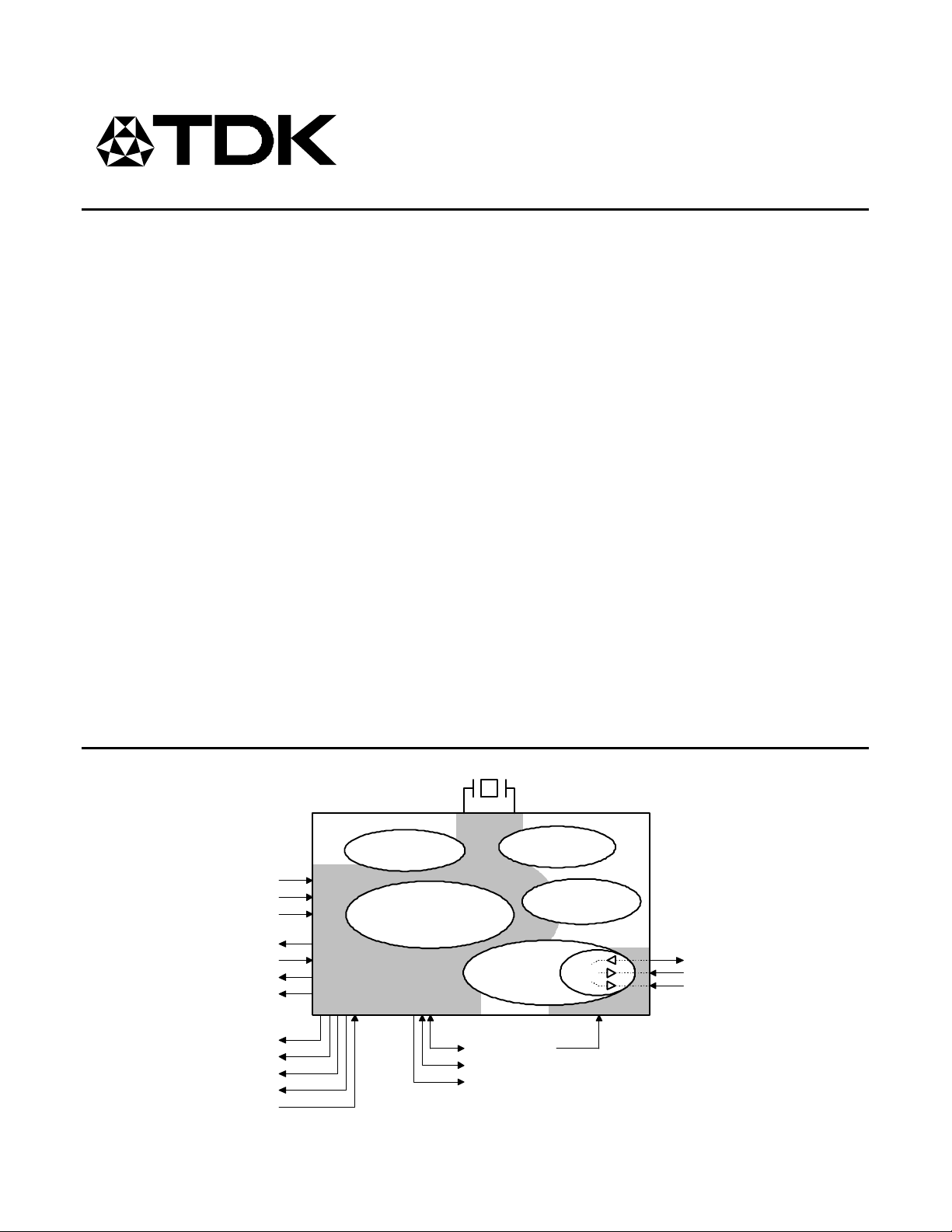
ASRCH
RING
DTR
TxCLK
TxD
RxD
RxCLK
RI
CTS
DCD
DSR
RTS
BLOCK DIAGRAM
RAM
CPU
AFE
USR10
USR11
RELAY
ROM
HBDEN
MAC
Hybrid
RxA
TxAP
TxAP
Page 2

73M2901/5V
Advanced Single
Chip Modem
HARDWARE DESCRIPTION
The 73M2901/5V is designed for a single +5 volt
supply with low power consumption (~250mW @ 5
volts). The modem supports automatic standby idle
mode. The modem will also accept a request to
power down from the DTE via hardware control. No
additional major components are required to
complete the modem core logic. The modem
provides direct firmware LED support via port pins.
HARDWARE FEATURES
· Fully self-contained. “AT” Command interpreter
and data pump
· User pin available
· Synchronous serial data I/O available
· Asynchronous serial port
· On-chip hybrid driver.
· Autobaud capability from 300bps to 9600bps
POWER SUPPLY
Power is supplied to the 73M2901/5V via the VPD and
VPA pins. The 73M2901/5V is designed for a single
+5 (+/-10%) volt supply and for low power consumption
(~250mW @ 5 volts). Ground Reference is provided
at the VND and VNA pins.
LOW POWER MODE
The TDK 73M2901/5V supports a low power mode.
If the low power standby option is enabled the
73M2901/5V will go into a power saving mode when
idle. The oscillator will be running, clocks will be
supplied to the UART, timers and interrupt blocks;
but no clocks will be supplied to the CPU. Instruction
processing and activity on the internal busses is
halted. Normal operation is resumed when an
interruption such as DTR, RING or ASRCH (any
character send to the 73M2901/5V) is requested or
when a reset occurs.
ANALOG LINE / HYBRID INTERFACE
The 73M2901/5V provides a differential analog
output (TXAP and TXAN) and a single-ended analog
input (RXA) with internal A/D and D/A converters. A
driver is provided for an internal hybrid function.
The internal hybrid driver is capable of driving an
external load matching impedance and a linecoupling transformer. If an external hybrid is to be
used, the on-chip hybrid drivers can be reconfigured
to drive a minimum load of 50kW and thus reduce
the driver’s power consumption.
The hybrid configuration is controlled by the state of
the HBDEN pin. For driving a line-coupling
transformer, HBDEN should be pulled high. For
driving an external hybrid (load on TXAP and TXAN
is 50kW or larger), HBDEN should be pulled low.
The 73M2901/5V provides firmware control for a
hook relay driver (RELAY) as well as interrupt
support for a ring detect opto-coupler (RING).
INTERRUPT PINS
The external interrupt sources, DTR, ASRCH and RING,
come from dedicated input pins of the same name.
DTR informs the 73M2901/5V that the host has
requested the 73M2901/5V perform a specific
function. The actual particulars of that function can
be changed by “AT” commands (described in full in
the TDK 73M2901 User’s Guide).
ASRCH informs the 73M2901/5V that the host is
passing data to the 73M2901/5V over the DTE
interface. This instructs the 73M2901/5V to begin
looking for valid “AT” commands. This pin needs to
be connected to the TXD pin.
RING informs the 73M2901/5V that the external
DAA circuitry has detected a ring signal.
CRYSTAL OSCILATOR
The TDK 73M2901/5V single chip modem can use
an external 11.0592 MHz reference clock or can
generate such a clock using only a crystal and two
capacitors. If an external clock is used, it should be
applied to OSCIN.
SPECIFYING A CRYSTAL
The manufacturer of a crystal resonator verifies its
frequency of oscillation in a test set-up, but to
ensure that the same frequency is obtained in the
application, the circuit conditions must be the same.
The TDK 73M2901/5V modem requires a parallel
mode (antiresonant) crystal, the important
specifications of which are as follows:
Mode: Parallel (antiresonant)
Frequency: 11.0592 MHz
Frequency tolerance: ±50 ppm at initial
temperature.
Temperature drift: ±50 ppm additional over full
Range.
Load capacitance: 18pF or 20pF
ESR: 75W max.
Drive level: Less than 1mW.
2
Page 3
Advanced Single
RESET
A reset is accomplished by holding the RESET pin
high. To ensure a proper power-on reset, the reset
pin must be held high for a minimum of 3m s. At
power on, the voltage at VPD, VPA, and RESET
must come up at the same time for a proper reset.
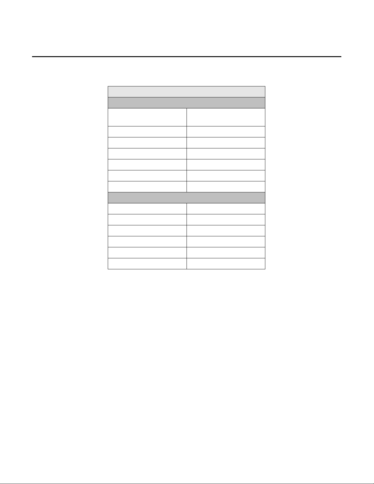
PIN DESCRIPTIONS
POWER PIN DESCRIPTION
PIN NAME 32-PIN 44-PIN TYPE DESCRIPTION
VPA 15 16 I Positive analog voltage (+ Analog Supply)
VNA 21 22 I Negative analog voltage. (Analog Ground)
VPD 6, 25,
29
VND 5, 22,
26
2,12,
27, 33
11, 24,
44, 28
I Positive digital voltage (+ Digital Supply)
I Negative digital voltage. (Digital Ground)
ASYNCHRONOUS AND SYNCHRONOUS SERIAL
DATA INTERFACE
The serial data interface consists of the TXD and
RXD data paths (LSBit shifted in and out first,
respectively); and the TXCLK and RXCLK serial
clock outputs associated with the data pins;
CTS/RTS flow control; DCR, DSR and DTR. In
synchronous mode, the data is passed at the bit rate
(tolerance is +1%, -2.5%).
73M2901/5V
Chip Modem
ANALOG INTERFACE PIN DESCRIPTION
PIN NAME 32-PIN 44-PIN TYPE DESCRIPTION
RXA 20 21 I Receive analog data
TXAN 16 17 O Transmit Analog TXAP 17 18 O Transmit Analog +
HBDEN 14 15 I 2w/4w hybrid driver enable pin
0 = Driver configured for 50kW or greater load (Tie to VND)
1 = Driver configured for driving line-coupling transformer (Tie to
VPD)
VBG 19 20 O
VREF 18 19 O
Analog Band Gap voltage reference pin (0.1m F to VNA)
Analog reference voltage pin (0.1m F to VNA)
EXTERNAL INTERRUPTS PIN DESCRIPTIONS
PIN NAME 32-PIN 44-PIN TYPE DESCRIPTION
RING
ASRCH
DTR
2
1
32
39
38
37
I
External interrupt – Line interface ring detection circuitry input
I
External interrupt – Autobaud detection, connected to TXD
I
External interrupt – DTE DTR signal input
3
Page 4
73M2901/5V
Advanced Single
Chip Modem
PIN DESCRIPTIONS (continued)
OSCILLATOR PIN DESCRIPTION
PIN NAME 32-PIN 44-PIN TYPE DESCRIPTION
OSCIN 24 26 I Crystal input for internal oscillator, also input for external
source.
OSCOUT 23 25 O Crystal oscillator output.
DIGITAL INTERFACE PIN DESCRIPTION
PIN NAME 32-PIN 44-PIN TYPE DESCRIPTION
RESET 13 9 I Resets 73M2901/5V
RXCLK 31 36 O Receive Data Synchronous Clock
RXD 30 35 O Serial output to DTE.
TXCLK 28 31 O Transmit Data Synchronous Clock
TXD 27 30 I Serial data input from DTE.
USR10 12 8 I/O This pin can optionally be configured as an active low detect
pin. This can be used to implement such functions as “parallel-
pick-up”, “line-in-use”, or “seize” detect.
USR11 11 7 I/O Programmable I/O port. This pin can ooptionnaly be used to
control an external switch for Caller ID decoding operations.
RTS (USR12) 10 6 I Request to Send
CTS (USR13) 9 5 O Clear to Send
DSR (USR14) 8 4 O Data Set Ready
DCD (USR15) 7 3 O Data Carrier Detect
RI (USR16) 4 43 O Ring Indicator
RELAY (USR17) 3 40 O Relay driver output
4
Page 5
73M2901/5V
Advanced Single
Chip Modem
ELECTRICAL SPECIFICATIONS
ABSOLUTE MAXIMUM RATINGS
Operation above maximum rating may permanently damage the device.
PARAMETER RATING
Supply Voltage -0.5V to +7.0V
Pin Input Voltage -0.5V to VPD + 0.5V
Storage Temperature -55ºC to 150°C
RECOMMENDED OPERATING CONDITIONS
PARAMETER RATING
Supply Voltage +5.0V (+/-10%)
Oscillator Frequency 11.0592MHz +/- 50ppm
Operating Temperature -40C to +85°C
TRANSMITTER
PARAMETER CONDITIONS MIN NOM MAX UNIT
ITU Guard Tone Power 550Hz (relative to carrier)
1800Hz (relative to carrier)
Calling Tone 1300Hz -11 -9.0 dBm01
Answer Tone Power 2225/2100Hz -11 -9.0 dBm01
DTMF Transmit Power High band tones
Low band tones
-5
-8
-8.0
-10
-3.5
-6.5
-6.0
-2
-5
-8.0
dB
dB
dBm01
1
dBm0 refers to the TDK recommended DAA ( 8dB loss from Transmit pins to the line and 5dB loss from the line to the Receive pin). Results
may vary depending on selected DAA. 0dBm = 0.775V
. dBm = 10log {Vrms2/[(1mW)(600O)]}
rms
5
Page 6
73M2901/5V
Advanced Single
Chip Modem
ELECTRICAL SPECIFICATIONS (continued)
MAXIMUM TRANSMIT LEVELS
Vref=2.25V; VPA=5.0V
Transmit type Maximum differential line
QAM -5.5
DPSK -3.4
FSK -1.2
DTMF (high tone) -6.0
DTMF (low tone) -8.0
DTMF (total) -3.9
Vref=1.25V; VPA=5.0V
level (dBm0)
QAM -9.6
DPSK -7.4
FSK -5.3
DTMF (high tone) -7.9
DTMF (low tone) -9.8
DTMF (total) -5.7
Note: The recommended DAA (see the TDK 73M2901 Reference Manual) will result in approximately 8dB loss from the transmit pins to the
phone line. This includes the loss through the line matching impedance (475W resistor), transformer, and solid state off-hook relay.
6
Page 7

73M2901/5V
Advanced Single
Chip Modem
ELECTRICAL SPECIFICATIONS (continued)
TRANSMITTER
PARAMETER CONDITIONS MIN NOM MAX UNIT
Gain Adjust
Tolerance
Transmit Gain Boost SFR 96h bit 1 (TXBOOST) = 1 4.8 5.1 5.4 dB
Total Harmonic
Distortion (THD)
Intermod Distortion At output (TXAP-TXAN)
Power Supply
Rejection Ratio
RECEIVER
PARAMETER CONDITIONS MIN NOM MAX UNIT
Carrier Detect On Tip and Ring -43.0 dBm01
Carrier Detect Off Tip and Ring -48.0 dBm01
Carrier Detect Hysteresis Tip and Ring 2.0 dB
Receive Level Tip and Ring -43.0 -9.0 dBm01
Idle Channel Noise 0.2kHz - 4.0kHz -70 -65 dB
By step
1Khz sine wave at output (TXAP-TXAN)
1.5Vpk(2.7dBm) for Vref=1.25V
2.4Vpk (6.8dBm) for Vref=2.25V
THD = 2nd and 3rd harmonic.
1.0kHz, 1.2 kHz sine waves summed
2.0Vpk for Vref=1.25V
2.4Vpk for Vref=2.25V
Refer to CTR21 specification for complete
description of requirements
-30 dBm signal at VPA
300Hz – 30kHz. Measured TXAP to TXAN.
-0.3 0 0.3 dB
-50 dB
each unwanted
frequency
component
sum of
unwanted
frequency
components in
pass band
-33
-20
30.0
below
low
tone
dB
dB
dB
7
Page 8

73M2901/5V
Advanced Single
Chip Modem
ELECTRICAL SPECIFICATIONS (continued)
RECEIVER (continued)
PARAMETER TEST CONDITION MIN NOM MAX UNITS
Input Impedance RXA 150 --- --Receive Gain
Boost
Level at RXA
Total Harmonic
Distortion (THD)
SFR 96h bit 2 (Rxgain) = 1 2.7 3.0 3.3 dB
VREF=1.25V 0.587 Vpk Maximum Input
VREF=2.25V 1.069 Vpk
1kHz 450mV-pk on RXA
THD = 2nd and 3rd harmonic.
-70 -50 dB
DC CHARACTERISTICS
kW
PARAMETER SYMBOL
Input Low Voltage
(Except OSCIN,RESET)
Input Low Voltage
OSCIN,RESET
Input High Voltage
(Except OSCIN,RESET)
Input High Voltage
OSCIN,RESET
Output Low Voltage
(Except OSCOUT)
Output Low Voltage
OSCOUT
Output High Voltage
(Except OSCOUT)
Output High Voltage
OSCOUT
Input Leakage Current
(Except OSCIN)
Input Leakage Current
OSCIN
VIL -0.5 0.2Vcc V
VIL -0.5 0.2 Vcc V
VIH 0.5 Vcc Vcc + 0.5 V
VIH 0.7 Vcc Vcc + 0.5 V
VOL IOL = 4mA 0.45 V
VOLOSC IOL = 3.0mA 0.7 V
VOH IOH = -4mA Vcc – 0.45 V
VOHOSC IOH =-3.0mA Vcc – 0.9 V
IIH Vss < Vin < Vcc 1
IIH Vss < Vin < Vcc 1 30
CONDITION MIN NOM MAX UNIT
m A
m A
8
Page 9

73M2901/5V
Advanced Single
Chip Modem
ELECTRICAL SPECIFICATIONS (continued)
DC CHARACTERISTICS
PARAMETER SYMBOL
5V Operations
Maximum Power Supply
Normal Operation @ 5V
HBDEN pulled high
Maximum Power Supply
Normal Operation @ 5V
HBDEN pulled low
Maximum Digital Power
Supply @ 5V
Maximum Analog Power
supply @ 5V
HBDEN pulled high
Maximum Analog Power
Supply @ 5V
HBDEN pulled low
Maximum Power Supply
Idle Mode @ 5V
Maximum Power Supply
Power Down Mode @ 5V
DC CHARACTERISTICS
PARAMETER CONDITION MIN NOM MAX UNIT
Vbg Vcc=5V 1.19 1.25 1.31 V
Vref Vcc=5V – no boost 1.19 1.25 1.31 V
Vref Vcc=5V + internal boost 2.14 2.25 2.36 V
5 Volts detection threshold 3.8 4.2 4.5 V
IDD1 30pF/pin 51 62 mA
IDD1 30pF/pin 35 43 mA
IDDd 30pF/pin 31 37 mA
IDDah1 30pF/pin 20 25 mA
IDDah0 30pF/pin 4 6 mA
IDD2 30pF/pin 11 15 mA
IDD3 30pF/pin 4 10
CONDITION MIN NOM MAX UNIT
m A
9
Page 10

73M2901/5V
Advanced Single
Chip Modem
FIRMWARE DESCRIPTION2
An “AT” command interpreter provides command
and configuration of the 73M2901/5V. This provides
the user a uniform interface to control the modem in
embedded applications.
The signal processing is performed by obtaining
data from and providing data to the integrated A/D
converter. A MAC hardware processor is provided
for computation.
To provide maximum flexibility, the system host
processor can access the internal RAM and Control
Register space in the modem. This will allow the
OEM user to modify parameters such as filter
response, transmit levels through the AT command
set using proprietary commands. The host
processor can also access the modem I/O port pins,
providing extended I/O capability.
FIRMWARE REQUIREMENTS
The modem always powers up in the idle (on hook)
mode. “AT” commands are issued via the serial
interface from the host. All modem configuration
commands are received in this manner. The data
modem firmware is contained in an internal ROM.
The firmware will automatically enter a power saving
idle mode if the modem is on hook and there are no
incoming host commands. The modem
automatically powers up upon receiving the next
command. This power up sequence occurs without
delay to the host. This function, while saving power,
is transparent to the host processor and can be
disabled by the host via an “AT” command. The
host can also program the modem to power down
via external pin (DTR) or via a firmware command.
FIRMWARE FEATURES
· “AT” command set
· Supports data standards through V.22bis
· Provides DAA control firmware (e.g. ring detect,
hook control, line in use detection support)
· Multinational Call progress support (FCC68,
CTR21, JATE…)
· Caller ID capability
FSK demodulation (V23 or Bell202)
Intra 1st/2nd ring CID data operations
Post Line reversal CID data operations
· Interfaces with standard V.24/EIA-232 (3-5 volt
inverted level) serial interface using the built in
serial port and firmware control of port pins
· Provides tone generation and detection, four
imprecise and four precise call progress detect
filters
· Host access to program RAM provided
· User access to modem functions
2
For a detailed description of the firmware consult the TDK
73M2901 User’s Manual.
10
Page 11

DESIGN CONSIDERATIONS
TDK Semiconductor’s single chip modem solutions
include all the basic modem functions. This makes
these devices adaptable to a variety of applications.
Unlike digital logic circuitry, modem designs must
contend with precise frequency tolerances and verify
low level analog signals, to ensure acceptable
performance. Using good analog circuit design
practices will generally result in a sound design.
The crystal oscillator should be held to a 50ppm
tolerance. Following are additional
recommendations that should be taken into
consideration when starting new designs.
LAYOUT CONSIDERATIONS
Good analog/digital design rules must be used to
control system noise in order to obtain high
performance in modem designs. The more digital
circuitry present in the application, the more
attention to noise control is needed.
High speed, digital devices should be locally
bypassed, and the telephone line interface and the
modem should be located next to each other near
where the telephone line connection is accessed. It
is recommended that power supplies and ground
traces should be routed separately to the analog and
digital portions on the board. Digital signals should
not be routed near low level analog or high
impedance analog traces.
The 73M2901/5V should be considered a high
performance analog device. A 10m F electrolytic
capacitor in parallel with a 0.1m F Ceramic capacitor
should be placed between VPD and VND as well as
between VPA and VNA. A 0.1m F ceramic capacitor
should be placed between VREF and VNA as well
as VBG and VNA. Use of ground planes and large
traces on power is recommended.
The 73M2901/5V is the first of a series of parts with
different and/or additional features. In order to insure
full lay out compatibility for all the series, it is
recommended to implement three additional
resistors in the schematics as shown in the
recommended schematics arrangement (R11, R12
and R13).
73M2901/5V
Advanced Single
Chip Modem
transformer directly (with the required impedance
matching series resistor). Used in this configuration,
there is loss associated in both the receive path and
transmit path.
The line interface circuit shown on the following
page represents the basic components and values3
for interfacing the TDK 73M2901/5V analog pins to
the telephone line.
MODEM PERFORMANCE
CHARACTERISTICS
The curves presented in this data sheet define
modem IC performance under a variety of line
conditions typical of those encountered over public
service telephone lines.
BER VS. SNR
This test represents the ability of the modem to
operate over noisy lines with a minimum amount of
data transfer errors. Since some noise is generated
in the best dial up lines, the modem must operate
with the lowest signal to noise ratio (SNR) possible.
Better modem performance is indicated by test
curves that are closest to the BER axis. A narrow
spread between curves representing the four line
parameters indicates minimal variation in
performance while operating over a range of
aberrant operating conditions. Typically a DPSK
modem will exhibit better BER performance test
curves receiving in the low band (answer mode)
than in the high band (originate mode).
BER VS. RECEIVE LEVEL
This test measures the dynamic range of the
modem. Because signal levels vary widely over dial
up lines, the widest possible dynamic range is
desirable. The SNR is held constant at the indicated
values as the Receive level is lowered from very a
very high to a very low signal level. The width of the
bowl of these curves, taken at the BER point is the
measure of the dynamic range.
TELEPHONE LINE INTERFACE
Transmit levels at the line are dependent on the
interface used between the pins and the line. In
order to save having to provide external op-amps to
drive the line coupling transformer, the analog
outputs (TXAP and TXAN) have the capability to be
used as the hybrid drivers for connecting to the
3
TDK73M2901 Demo boards use the line interface shown on the
following page. Other designs may have different requirements
and thus will require different component values or a different
configuration. With the shown configuration, there is
approximately an 8dB loss in the transmit path, and approximately
a 5dB loss in the receive path.
11
Page 12

73M2901/5V
elephone
Advanced Single
Chip Modem
RXA
21K
R4R3
5.1K
To
--> RS232
level shifter
--> Host
microprocessor
JP1
10
9
8
7
6
5
4
3
2
1
HEADER 10
TXAP
TXAN
VCC
GND
TTL V24
signals
interface
R1
475
C1
0.033m
Recommended Line Interface
VCC
R11 0R
1
+ C2
10uF
2
R1
10K
GND
7
DCD
8
DSR
9
CTS
4
RI
10
RTS
32
DTR
31
RXC
30
RXD
27
TXD
1
ASRCH
28
TXC
R12
0R
13
RST
OSCIN
USR11
USR10/LIU
11 12
Y1
11.0592 MHZ
6
23 24 25 26
29
VPD
VPD
VPD
OSCOUT
RING
RELAY
2 3
R13
nc
5
VND
VREF
HBDEN
22
VND
VPA
VNA
VBG
RXA
TXAP
TXAN
VND
VCC
GND
U1
2901_P32
15
21
18
19
14
20
17
16
C1
27PF
C3
33PF
T1
Midcom 671-8005
GND
GND
VPA
C4 100nF
C5 100nF
VNA
VCC
T
Line
R2 21K
R3 5.1K
R4 470
.033UF
T1
2
3
C7
SEC
4
671-8005
PRI
1
Recommended Schematics Arrangement
12
Page 13

TYPICAL USA APPLICATION SCHEMATICS
73M2901/5V
Advanced Single
Chip Modem
13
Page 14

73M2901/5V
Advanced Single
Chip Modem
BER VS SNR BER VS RECEIVE LEVEL
V.22bis
3002A Line, 5.0V, 25CV.22bis
1.00E+00
1.00E-01
Answer
Originate
1.00E-02
1.00E-03
Bit Error Rate
1.00E-04
1.00E+00
1.00E-01
1.00E-02
1.00E-03
Bit Error Rate
1.00E-04
3002A Line, 5.0V, 25C
Answer
Originate
1.00E-05
1.00E-06
10 11 12 13 14 15 16 17 18 19
SNR (Rx Signal/3k Hz) (dB)
1.00E-05
1.00E-06
4
8 12 16 20 24 28 32 36 40 44
Receive Level (dBm)
14
Page 15

32 PIN PLCC PIN-OUT
PIN PIN NAME PIN PIN NAME
1 ASRCH 17 TXAP
2 RING 18 VREF
3 RELAY 19 VBG
4 RI 20 RXA
5 VND 21 VNA
6 VPD 22 VND
7 DCD 23 OSCOUT
8 DSR 24 OSCIN
9 CTS 25 VPD
10 RTS 26 VND
11 USR11 27 TXD
73M2901/5V
Advanced Single
Chip Modem
12 USR10 28 TXCLK
13 RESET 29 VPD
14 HBDEN 30 RXD
15 VPA 31 RXCLK
16 TXAN 32 DTR
44 PIN TQFP PIN-OUT
PIN PIN NAME PIN PIN NAME PIN PIN NAME PIN PIN NAME
1 N/C 12 VPD 23 N/C 34 N/C
2 VPD 13 N/C 24 VND 35 RXD
3 DCD 14 N/C 25 OSCOUT 36 RXCLK
4 DSR 15 HBDEN 26 OSCIN 37 DTR
5 CTS 16 VPA 27 VPD 38 ASRCH
6 RTS 17 TXAN 28 VND 39 RING
7 USR11 18 TXAP 29 N/C 40 RELAY
8 USR10 19 VREF 30 TXD 41 N/C
9 RESET 20 VBG 31 TXCLK 42 N/C
10 N/C 21 RXA 32 N/C 43 RI
11 VND 22 VNA 33 VPD 44 VND
15
Page 16

73M2901/5V
Advanced Single
Chip Modem
MECHANICAL DRAWINGS
32-Pin PLCC
16
Page 17

MECHANICAL DRAWINGS (continued)
73M2901/5V
Advanced Single
Chip Modem
44-Pin TQFP (JEDEC LQFP)
17
Page 18

73M2901/5V
Advanced Single
Chip Modem
PACKAGE PIN DESIGNATIONS
(Top View)
CAUTION: Use handling procedures necessary for a
static sensitive component.
32-Lead PLCC 44-Pin TQFP
73M2901-32IH/5 73M2901-IGT/5
ORDERING INFORMATION
PART DESCRIPTION ORDER NUMBER PACKAGING MARK
73M2901/5V
32-Pin Plastic Leaded Chip Carrier
73M2901/5V
44-Pin Thin Quad Flat Pack
No responsibility is assumed by TDK Semiconductor Corporation for use of this product nor for any infringements of patents and trademarks
or other rights of third parties resulting from its use. No license is granted under any patents, patent rights or trademarks of
TDK Semiconductor Corporation, and the company reserves the right to make changes in specifications at any time without notice.
Accordingly, the reader is cautioned to verify that the data sheet is current before placing orders.
TDK Semiconductor Corp., 2642 Michelle Dr., Tustin, CA 92780, (714) 508-8800, FAX (714) 508-8877, www.tdksemiconductor.com
73M2901-32IH/5 73M2901-32IH
73M2901-IGT/5 73M2901-IGT
Ó TDK Semiconductor Corporation 08/30/01 Rev. D
Revision:
18
Page 19

73M2901/5V
Advanced Single
Chip Modem
August 22, 2001 Removed 5V pin callouts from package drawing.
August 30, 2001 Updated Mechanical Drawing
19
 Loading...