

Page 1
www.DataSheet.co.kr
Datasheet pdf - http://www.DataSheet4U.net/
Product Description: 26 inch TFT-LCD PANEL
AUO Model Name: T260XW02 VC
Customer Part No/Project Name:
Customer Signature Date AUO Date
PDF created with FinePrint pdfFactory Pro trial version www.pdffactory.com
Page 2

Document Version: 1.0
www.DataSheet.co.kr
Datasheet pdf - http://www.DataSheet4U.net/
Date:2006/12/1
Product Functional Specification
26” Color TFT-LCD Module
Model Name: T260XW02 VC
(QDI Model: QD26HL0206)
() Preliminary Specification
(*) Final Specification
PDF created with FinePrint pdfFactory Pro trial version www.pdffactory.com
Page 3

This specification sheet is for model name change, since AUO merged QDI from 2006/10/1
www.DataSheet.co.kr
Datasheet pdf - http://www.DataSheet4U.net/
This Specification Sheet keep the original QDI Model name and Spec.
New Model name and old model name comparison table as following:
AUO QDI
Model Name T260XW02 VC QD26HL0206
Change Item 1. Carton Printing format
2. Product Serial label format
PDF created with FinePrint pdfFactory Pro trial version www.pdffactory.com
Page 4
www.DataSheet.co.kr
Datasheet pdf - http://www.DataSheet4U.net/
Revision History
REV.
Date ECN NO. Change Content
1 12/1 Change AUO product name
PDF created with FinePrint pdfFactory Pro trial version www.pdffactory.com
Page 5

Content List
www.DataSheet.co.kr
Datasheet pdf - http://www.DataSheet4U.net/
Page
1. Application 5
2. Overview 5
3. General Specifications 5
4. Input Terminals 6
5. Absolute Maximum Ratings 5
6. Electrical Characteristics 11
7. Timing Characteristics 15
8. Input Signals, Basic Display Colors and Gray
Scale of Each Color 17
9. Optical Characterics 18
10. Display Quality 21
11. Handling Precautions 21
12. Reliability Test Items 21
13. Others 22
14. Drawing 23
PDF created with FinePrint pdfFactory Pro trial version www.pdffactory.com
Page 6
1. Application
www.DataSheet.co.kr
Datasheet pdf - http://www.DataSheet4U.net/
This specification applies to a color TFT-LCD module, QD26HL02
2. Overview
This module is a color active matrix LCD module incorporating amorphous silicon TFT
(Thin Film Transistor). It is composed of a color TFT-LCD panel; driver ICs, control circuit and
power supply circuit and a backlight unit. Graphics and texts can be displayed on a 1366×3×768
dots panel with 16.7 million colors by using the LVDS (Low Voltage Differential Signaling)
interface, 8-bit driving method and supplying +12V DC supply voltage for TFT-LCD panel
driving.
The TFT-LCD panel used for this module has very high aperture ratio. A low-reflection and
higher-color-saturation type color filter is also used for this panel. Therefore, high-brightness
and high-contrast image, which is suitable for the LCD TV,HDTV and multimedia use, can be
obtained by using this module.
[Features]
1) High aperture panel; high-brightness
2) Brilliant and high contrast image.
3) High speed response
4) WXGA resolution. 16:9
5) LVDS interface.
6) QSV technology
7) Wide viewing angle.
3. General Specifications
Parameter Specifications Unit
Display size 66.05 (26") Diagonal cm
Active area
Pixel format
575.769 (H)×323.712 (V)
1366 (H)×768 (V)
mm
Pixel
(1 pixel = R+G+B dots)
Pixel pitch
0.4215 (H) × 0.4215 (V)
mm
Pixel configuration R,G,B vertical stripe
Display mode Normally Black
Unit outline dimensions 626 x 373 mm
Thickness Max. 47.3 mm
Weight Typ 40.9 g
Surface treatment Anti-glare(13%) and
hard-coating 3H
Lamp Quantity 8 U shape pcs
PDF created with FinePrint pdfFactory Pro trial version www.pdffactory.com
Page 7
www.DataSheet.co.kr
Datasheet pdf - http://www.DataSheet4U.net/
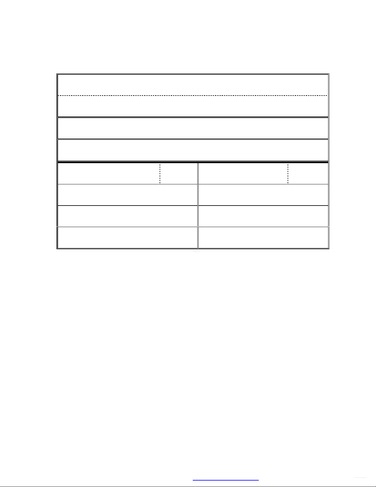
4. Input Terminals
4-1. TFT-LCD panel driving
CN1 (LVDS signals and +12V DC power supply)
Connector on Panel : FI-X30SSL-HF(Manufactured by JAE) or Equivalent
Mating connector : FI-30C2L (Manufactured by JAE) or Equivalent
Pin No
Symbol Description Default
1 VCC +12V, DC, Regulated
2 VCC +12V, DC, Regulated
3 VCC +12V, DC, Regulated
4 VCC +12V, DC, Regulated
5 GND Ground and Signal Return
6 GND Ground and Signal Return
7 GND Ground and Signal Return
8 GND Ground and Signal Return
9 LVDS Option Low/Open for Normal (NS), High for JEIDA Default NS type
10 Reserved N.C.
11 GND Ground and Signal Return for LVDS
12 RXIN0- LVDS Channel 0 negative
13 RXIN0+ LVDS Channel 0 positive
14 GND Ground and Signal Return for LVDS
15 RXIN1- LVDS Channel 1 negative
16 RXIN1+ LVDS Channel 1 positive
17 GND Ground and Signal Return for LVDS
18 RXIN2- LVDS Channel 2 negative
19 RXIN2+ LVDS Channel 2 positive
20 GND Ground and Signal Return for LVDS
21 RXCLKIN- LVDS Clock negative
22 RXCLKIN+ LVDS Clock Positive
23 GND Ground and Signal Return for LVDS
24 RXIN3- LVDS Channel 3 negative
25 RXIN3+ LVDS Channel 3 positive
26 GND Ground and Signal Return for LVDS
PDF created with FinePrint pdfFactory Pro trial version www.pdffactory.com
Page 8

27 Reserved N.C.
www.DataSheet.co.kr
Datasheet pdf - http://www.DataSheet4U.net/
28 Reserved N.C.
29 GND Ground and Signal Return
30 GND Ground and Signal Return
【
Note 1】All GND(ground) pins should be connected together.
【Note 2】All VDD (power supply) pins should be connected together.
PDF created with FinePrint pdfFactory Pro trial version www.pdffactory.com
Page 9

4-2 Interface block diagram
www.DataSheet.co.kr
Datasheet pdf - http://www.DataSheet4U.net/
PDF created with FinePrint pdfFactory Pro trial version www.pdffactory.com
Page 10

4-3. Backlight driving
www.DataSheet.co.kr
Datasheet pdf - http://www.DataSheet4U.net/
4-3-1. Inverter Connector
Connector on Inverter : S14B-PH-SM3(Manufactured by JST) or Equivalent
Mating connector : PHR-14 (Manufactured by JST) or Equivalent
Pin No Symbol Description Default
1 VIN Operating Voltage Supply, +24V DC regulated 24V
2 VIN Operating Voltage Supply, +24V DC regulated 24V
3 VIN Operating Voltage Supply, +24V DC regulated 24V
4 VIN Operating Voltage Supply, +24V DC regulated 24V
5 VIN Operating Voltage Supply, +24V DC regulated 24V
6 BLGND Ground and Current Return GND
7 BLGND Ground and Current Return GND
8 BLGND Ground and Current Return GND
9 BLGND Ground and Current Return GND
10 BLGND Ground and Current Return GND
11 ADIM
(1)
GND (0V) 80% Lum / Open (1.6V) 100% Lum / High
(3.3V) 120% Lum
12 ON/OFF BL On-Off: Open/High (3.3V) for BL On as default On
PWM Dimming: Open/High (3.3V) for 100% Lum
13 PDIM
(2)
Analog Dimming: GND (0V) 20% Lum/ Open or High
(3,3V) 100% Lum
14
PWM
Selection
(3)
GND: Duty Signal to 13pin, Open/High(3.3V): Analog
Voltage to 13 pin
[Note]
(1) ADIM is control signal for Inverter’s output Power to Back Light Lamp Bulb. Input Signal should
be able to control Amplitude of Inverter Output voltage. From 0V to 3.3V, Inverter Output Voltage
should be able to vary to control Brightness of Lamp from 80% to 120% Luminescence variation.
(2) PDIM is PWM control input; i.e. for the given ADIM, this PDIM input should be able to control
Width of Voltage Burst of inverter output for Lamp Driving. This input can have two type of input;
Ordinary default setting will be DC level signal using Saw Tooth Wave control for PWM duty
control. The other setting is Duty Signal Input with 3.3V TTL specification. These two method
should be decided by 14th Pin input setting.
(3) (3) 14 Pin is selection pin for PWM control method; if this pin is connected to GND, PDIM input of
100%
100%
Analog
13th Pin should have Logic Level Duty Signal for PWM control. If this is set to High or Open, 13th
Pin should have DC level signal therefore the Inverter should have Saw Tooth Wave Generator to
generate internal PWM signal. Default setting is “Analog”, means when it is “Not Connected”, 13th
pin of PWM control should be have DC Level signal for PWM.
PDF created with FinePrint pdfFactory Pro trial version www.pdffactory.com
Page 11

4-3-2. Lamp connector
www.DataSheet.co.kr
Datasheet pdf - http://www.DataSheet4U.net/
Back Light Lamp Connectors and Pin Assignment are as follows.
Connectors attached to Lamp Lead : BHR-04VS-1(JST)
Mating connectors for Inverter output : SM02(12.0)B-BHS-1-TB(JST) or
4002P0220T(LANDWIN
Pin No
Symbol Description Default
1 CFL HOT High Voltage AC Signal
2 N.C. Spacing for High Voltage Clearance
3 CFL HOT Return for High Voltage AC Signal
5. Absolute Maximum Ratings
LCD module
Parameter Symbol Condition
+12V supply voltage V
Storage temperature Tstg
Operating temperature (Ambient) Topa
【
Note1】Humidity:90%RH Max. at Ta≦40℃.
DD
Ta=25℃ -0.3 〜 +14.0
-
- 0 〜 +50 ℃
Ratings Unit Remark
V
-
20 〜 +60
℃ 【
Note1
】
Maximum wet-bulb temperature at 39℃ or less at Ta>40℃.
No condensation.
PDF created with FinePrint pdfFactory Pro trial version www.pdffactory.com
Page 12

6. Electrical Characteristics
Rise time
0V
T5 T6 T7 T3 T4
www.DataSheet.co.kr
Datasheet pdf - http://www.DataSheet4U.net/
6-1.TFT-LCD panel driving Ta
25℃
Parameter Symbol Min. Typ. Max. Unit Remark
V
Supply voltage V
DD
DD
Current dissipation IDD
Permissive input ripple
VRP
11.4 +12.0 12.6
-
340 650
-
-
120 mV p-p VDD=+12V
V
mA 【
【
Note2】
Note3】
voltage
Differential input High
VTH
-
-
100
mV
VCM=+1.2V
threshold voltage Low
Rush current I
VTL
RUSH
-100
-
-
mV
3.0 A
【
Note1
】
470uS
【
Note1】 VCM : Common mode voltage of LVDS driver.
【
Note2】
Power On-off sequence
90%
90%
Power Supply For
LCD
10%
10%
T1 T2
Interface Signal
10%
Valid
10%
50μs<T1,T6≦10 ms 0.5ms<T2,T5≦50 ms 200ms<T3,T4 T7>1 s
Power for LAMP
Lamp
【
Note3】 Maximum current condition; Change to 1x1 dot checker board pattern.
VDD=+12V
R G B R G B
R G B R G B
R G B R G B
R G B R G B
:0 GS
:255 GS
6-2. Backlight driving
The backlight system is a direct-lighting type with 8 U shape CCFT (Cold Cathode
Fluorescent Tube).
The characteristics of the lamp are shown in the following table.
Parameter Symbol Min.
Typ. Max. Unit
Remark
=
PDF created with FinePrint pdfFactory Pro trial version www.pdffactory.com
Page 13

Lamp current range I
Vrms
Vrms
www.DataSheet.co.kr
Datasheet pdf - http://www.DataSheet4U.net/
5.5 6 6.5 mAr
L
【
Note1】
ms
Lamp voltage V
Lamp power
1000 Vrms
L
PL
6
W
【
Note2】IL=mA
consumption
Lamp frequency F
Established starting
42 45 48 kHz
L
Vs 1100 1500
voltage
1200 1500
Lamp life time L
50000
L
hour
【
Note3】
Ta=25
℃
Ta=0
【
Note5】
℃ 【
【
Note1】 Lamp current is measured with current meter for high frequency as shown
below.
Note4
】
【
Note2】 Calculated Value for reference ( I
【
Note3】 Lamp frequency may produce interference with horizontal synchronous
L × V L)
frequency, and this may cause beat on the display. Therefore lamp frequency
shall be detached as much as possible from the horizontal synchronous
frequency and from the harmonics of horizontal synchronous to avoid
interference.
【
Note4】 The voltage above this value should be applied to the lamp for more than 1
second to start-up. Otherwise the lamp may not be turned on.
【
Note5】 Lamp life time is defined as the time when either ① or ② occurs in the
continuous operation under the condition of Ta = 25℃ and IL = 6mArms.
① Brightness becomes 50 % of the original value under standard condition.
② Kick-off voltage at Ta = 0℃ exceeds maximum value.
【
Note6】 The performance of the backlight, for example life time or brightness, is much
influenced by the characteristics of the DC-AC inverter for the lamp. When you
design or order the inverter, please make sure that a poor lighting caused by the
mismatch of the backlight and the inverter (miss-lighting, flicker, etc.) never
occur. When you confirm it, the module should be operated in the same
condition as it is installed in your instrument.
【
Note7】The lamp wire length is TBD mm(from AL back cover surface to connector, not
PDF created with FinePrint pdfFactory Pro trial version www.pdffactory.com
Page 14

including connector length)
Supply Input
Supply Input
www.DataSheet.co.kr
Datasheet pdf - http://www.DataSheet4U.net/
6-3 Backlight inverter
6-3-1. Inverter Electrical Characteristics
Parameter
Power
Symbol Min. Typ. Max. Unit Notes
V
22.8 24 25.2 Vdc
DDB
Voltage
Power
I
3000 3400 mA
DDB
Current
Power
PB 72 W
Consumption
6.4 Luminance Controls
Method Adjustment and Luminance Ratio PWM Selection Remark
Voltage
control
Adjustment – Continuous adjustment of
Luminance by adjusting the voltage
High/Open for max.
ADIM
3.3V1.6V/open0V
3.3V1.6V/open0V
PDIMLumratio
PWM
control
120%100%80%3.3V
120%100%80%3.3V
20%0V
20%0V
Adjustment- The luminance is controlled
by duty ratio of BRTP signal when PWM
Selection is GND and PWM signal is
inputted into BRTP termial.
Duty Ratio Luminance Ratio
0.2 20%(minimum)
1.0 100%
(maximum)
GND See PWM
timing
PDF created with FinePrint pdfFactory Pro trial version www.pdffactory.com
Page 15

6-5. PWM timing
A
www.DataSheet.co.kr
Datasheet pdf - http://www.DataSheet4U.net/
6-5-1. Timing diagram
- Outline
BRT
BRT
- Detail of A part
VBP
VBP
6-5-2. Each parameter
0≤tPWL≤50ms
tPWH
0≤tPWL≤50ms
0≤tPWL≤50ms
tPWL
tPW
PDF created with FinePrint pdfFactory Pro trial version www.pdffactory.com
Page 16

7. Timing characteristics of LCD module input signals
A D E F
www.DataSheet.co.kr
Datasheet pdf - http://www.DataSheet4U.net/
7-1. Timing characteristics
(This is specified at digital outputs of LVDS driver.)
Symbol Min Typ Max Unit Notes
ITIME
Frequency F
CLK
-
80 82 MHz DCLK
Hsync
Vsync
Data
Enable
Period t
Period t
Width-Active t
Frequency fH 44 48.54 52 kHz
CLK
HA
HC
12.2 12.5 - ns
1512 1648 1780
8 16 -
t
CLK
Frequency fv 47 60 63 Hz
Period t
Width-Active t
Horizontal back
774 810 -
VA
VC
t
HD
2 6 8 80 - t
tHA
CLK
porch
Horizontal front
tHF 16 186 - t
CLK
porch
Horizontal active t
Horizontal blanking t
Vertical back porch t
HE
HB
VD
1366 1366 1366 t
146 282 t
CLK
CLK
2 20 - tHA
Vertical front porch tVF 2 16 - tHA
Vertical active t
768 768 768 tHA
VE
Vertical blanking tVB 6 42 tHA
Notes : 1.The performance of electro-optical characteristics may be influenced by variance
of the vertical refresh rate.
2. Hsync period will be a double number of character (8).
7-2 Signal Timing Waveform(The time “B” is t
Data
ENAB
Sync
C
on horizontal timing and tVB on vertical timing)
HB
B
PDF created with FinePrint pdfFactory Pro trial version www.pdffactory.com
Page 17

0 0 0 0 0 0 0 0 0 0 0 0 0 0 0 1 1 1 1 1 1 1 1
0 0 0 0 0 0 0 1 1 1 1 1 1 1 1 0 0 0 0 0 0 0 0
0 0 0 0 0 0 0 1 1 1 1 1 1 1 1 1 1 1 1 1 1 1 1
1 1 1 1 1 1 1 0 0 0 0 0 0 0 0 0 0 0 0 0 0 0 0
1 1 1 1 1 1 1 1 1 1 1 1 1 1 1 0 0 0 0 0 0 0 0
1 1 1 1 1 1 1 1 1 1 1 1 1 1 1 1 1 1 1 1 1 1 1
0 0 0 0 0 0 0 0 0 0 0 0 0 0 0 0 0 0 0 0 0 0 0
1 0 0 0 0 0 0 0 0 0 0 0 0 0 0 0 0 0 0 0 0 0 0
0 1 1 1 1 1 1 0 0 0 0 0 0 0 0 0 0 0 0 0 0 0 0
1 1 1 1 1 1 1 0 0 0 0 0 0 0 0 0 0 0 0 0 0 0 0
0 0 0 0 0 0 0 0 0 0 0 0 0 0 0 0 0 0 0 0 0 0 0
0 0 0 0 0 0 0 0 1 0 0 0 0 0 0 0 0 0 0 0 0 0 0
0 0 0 0 0 0 0 1 0 1 1 1 1 1 1 0 0 0 0 0 0 0 0
0 0 0 0 0 0 0 1 1 1 1 1 1 1 1 0 0 0 0 0 0 0 0
0 0 0 0 0 0 0 0 0 0 0 0 0 0 0 0 0 0 0 0 0 0 0
0 0 0 0 0 0 0 0 0 0 0 0 0 0 0 0 1 0 0 0 0 0 0
0 0 0 0 0 0 0 0 0 0 0 0 0 0 0 1 0 1 1 1 1 1 1
0 0 0 0 0 0 0 0 0 0 0 0 0 0 0 1 1 1 1 1 1 1 1
www.DataSheet.co.kr
Datasheet pdf - http://www.DataSheet4U.net/
8. Input Signals, Basic Display Colors and Gray Scale of Each Color
Blue 0
Basic Color Gray Scale of Red
Green 0
Cyan 0
Red 1
Magenta 1 1 1 1 1 1 1 1 0 0 0 0 0 0 0 0 1 1 1 1 1 1 1 1
Yellow 1
White 1
Black 0
Colors &
Data Signal
Gray scale R0 R1 R2 R3 R4 R5 R6 R7 G0 G1 G2 G3 G4 G5 G6 G7 B0 B1 B2 B3 B4 B5 B6 B7
Black
0 0 0 0 0 0 0 0 0 0 0 0 0 0 0 0 0 0 0 0 0 0 0 0
ñ
1 0 0 0 0 0 0 0 0 0 0 0 0 0 0 0 0 0 0 0 0 0 0 0
Darker 0
ñ
ò
Bright 1
ò
0 1 1 1 1 1 1 1 0 0 0 0 0 0 0 0 0 0 0 0 0 0 0 0
Red 1
Black 0
Gray Scale of Green Gray Scale of Blue
ñ
0 0 0 0 0 0 0 0 1 0 0 0 0 0 0 0 0 0 0 0 0 0 0 0
Darker 0
ñ
ò
Bright 0
ò
0 0 0 0 0 0 0 0 0 1 1 1 1 1 1 1 0 0 0 0 0 0 0 0
Green 0
Black 0
ñ
0 0 0 0 0 0 0 0 0 0 0 0 0 0 0 0 1 0 0 0 0 0 0 0
Darker 0
ñ
ò
Bright 0
ò
0 0 0 0 0 0 0 0 0 0 0 0 0 0 0 0 0 1 1 1 1 1 1 1
Blue 0
á
â
á
â
á
â
á
â
á
â
á
â
á
â
á
â
á
â
0 : Low level voltage, 1 : High level voltage
PDF created with FinePrint pdfFactory Pro trial version www.pdffactory.com
Page 18

Photo detector
o
www.DataSheet.co.kr
Datasheet pdf - http://www.DataSheet4U.net/
Ta=25℃, VDD=+12V
Parameter Symbol Condition Min. Typ. Max. Unit Remark
Viewing
angle
L/R
U
D
θ21,θ22
θ11
θ12
CR>10 80 85 Deg.
80 85 Deg.
80 85 Deg.
range
Contrast ratio
Response time
Rise time
Fall time
Gray to gary
τr
τd
CRn θ=0°
τ
21
4
8 16 ms
600 1000
-
reponse time
Chromaticity of Wx 0.244 0.274 0.304
White (CIE 1931)
Wy 0.256 0.286 0.316
Chromaticity of Rx 0.612 0.642 0.672
Red (CIE 1931) Ry 0.306 0.336 0.366
Chromaticity of Gx 0.236 0.268 0.298
Green (CIE 1931)
Gy 0.565 0.595 0.625
Chromaticity of Bx 0.113 0.143 0.173
Blue (CIE 1931) By 0.032 0.062 0.092
Luminance of white
【Note4】
White Uniformity
Y
δ
L
W
400 500 Cd/m
-
ms
ms
ms
25
-
-
-
-
2
- 1.3
【Note1,4】
【Note2,4】
【Note3,4】
【Note4】
NTSC 72%
【Note5】
The measurement shall be executed 30 minutes after
※
= 6mArms)
ghting at rating. (typical condition : I
li
The optical characteristics shall be measured in a dark room or equivalent state with the
method shown in Fig.1 below.
(BM-5A: TOPCON)
Fig 1. Optical characteristics measurement
L
PDF created with FinePrint pdfFactory Pro trial version www.pdffactory.com
Page 19

www.DataSheet.co.kr
Datasheet pdf - http://www.DataSheet4U.net/
PDF created with FinePrint pdfFactory Pro trial version www.pdffactory.com
Page 20

【Note1】Definitions of viewing angle range:
time
τrτ
d
Black
Black
White
0%
10%
100%
90%
www.DataSheet.co.kr
Datasheet pdf - http://www.DataSheet4U.net/
【Note2】Definition of contrast ratio:
The contrast ratio is defined as the following.
Contrast Ratio (CR) =
Luminance (brightness) with all pixels
Luminance (brightness) with all pixels
【Note3】Definition of response time:
The response time is defined as the following figure and shall be measured by
switching the input signal for "black" and "white" .
(Relative Value)
Photo detector Output
【Note4】This shall be measured at center of the screen.
【Note5】Definition of white uniformity:
White uniformity is defined as the
following with five measurements
H/4
H/2
3H/4
PDF created with FinePrint pdfFactory Pro trial version www.pdffactory.com
Page 21

www.DataSheet.co.kr
Datasheet pdf - http://www.DataSheet4U.net/
δw =
Luminance of Center
Luminance (of every point other than center
PDF created with FinePrint pdfFactory Pro trial version www.pdffactory.com
Page 22

10. Display Quality
Serial Number Bar
www.DataSheet.co.kr
Datasheet pdf - http://www.DataSheet4U.net/
The display quality of the color TFT-LCD module shall be in compliance with the
Incoming Inspection Standard.
11.Handling Precautions
a) Be sure to turn off the power supply when inserting or disconnecting the cable.
b) Be sure to design the cabinet so that the module can be installed without any extra stress such as warp or twist.
c) Since the front polarizer is easily damaged, pay attention not to scratch it.
d) Wipe off water drop immediately. Long contact with water may cause
discoloration or spots.
e) When the panel surface is soiled, wipe it with absorbent cotton or other soft cloth.
f) Since the panel is made of glass, it may break or crack if dropped or bumped on
hard surface. Handle with care.
g) Since CMOS LSI is used in this module, take care of static electricity and injure
the human earth when handling.
h) Observe all other precautionary requirements in handling components.
i) This module has its circuitry PCBs on the rear side and should be handled carefully
in order not to be stressed.
j) Laminated film is attached to the module surface to prevent it from being scratched . Peel the film off
slowly just before the use with strict attention to electrostatic charges. Ionized air shall be blown over
during the action. Blow off the 'dust' on the polarizer by using an ionized nitrogen gun, etc..
12.Reliability test items
Test item Conditions
No.
1 High temperature storage test
2 Low temperature storage test
3 High temperature
& high humidity operation test
4 High temperature operation
test
5 Low temperature operation test
6 Vibration test (non-
Ta = 60℃ 240h
Ta =-20℃ 240h
Ta = 50℃ ; 80 %RH 240h
Ta = 60℃ 240h
Ta = 0℃ 240h
Frequency: 10〜500Hz, 1.0G , 20 min/each axis
operating)
7 Shock test
(non- operating)
Gravity : 100G
Pulse width : 2ms, half sine wave
Direction : ±X,±Y,±Z
Once for each direction.
13.Others
1) LCD Module Label:
Serial number Product Name
LWC295100001 QD26HL02 Rev.01
LWC295100001 Digital code 4, 5 is Date code.
Digital 4 (Year) 1: 2001, 2: 2002, 3:2003,….
Code
PDF created with FinePrint pdfFactory Pro trial version www.pdffactory.com
Page 23

Digital 5 (Month) 1: Jan, 2: Feb,… , A:Oct, B:Nov., C: Dec.
www.DataSheet.co.kr
Datasheet pdf - http://www.DataSheet4U.net/
2) Adjusting volume has been set optimally before shipment, so do not change any adjusted value. If adjusted
value is changed, the specification may not be satisfied.
3) Disassembling the module can cause permanent damage and should be strictly
avoided.
4) Please be careful since image retention may occur when a fixed pattern is displayed for a long time.
5) If any problem occurs in relation to the description of this specification, it shall be
resolved through discussion with spirit of cooperation.
PDF created with FinePrint pdfFactory Pro trial version www.pdffactory.com
Page 24

Front View
www.DataSheet.co.kr
Datasheet pdf - http://www.DataSheet4U.net/
14. Drawing
©Copyright AU Optronics, Inc.
Sep, 2006 All Rights Reserved.
No Reproduction and Redistribution Allowed
PDF created with FinePrint pdfFactory Pro trial version www.pdffactory.com
Page 25

www.DataSheet.co.kr
Datasheet pdf - http://www.DataSheet4U.net/
©Copyright AU Optronics, Inc.
Sep, 2006 All Rights Reserved.
No Reproduction and Redistribution Allowed
PDF created with FinePrint pdfFactory Pro trial version www.pdffactory.com
 Loading...