

Page 1

TCL
SERVICE MANUAL
CRT CHASSIS SY33
1、 Caution………………………………………………………………………2
2、 Specification…………………………………………………………………6
3、 Alignment Procedure……… ……………………………………………… 8
4、 Block Diagram…………… …………………………………………… … 13
5、 Circuit Theory Introduction…………………… …………………………14
6、 Troubleshooting ……… ………… …………… ………… ……………16
7、 Schematic Diagram ……………………… ………………………………18
8、 Main IC Introduction………… …… ……………………………………20
9、 BOM list…………………… ………………………………………………30
This manual is the latest at the time of printing, and does not
include the modification which may be made after the printing, by
the constant improvement of product
Page 2
CAUTION:
1、
Use of controls, adjustments or procedures other than those specified herein may result in
hazardous radiation exposure.
CAUTION: T O REDUCE THE RISK OF
CAUTION
RISK RISK OF OF ELECTRIELECTRICC
SHOCK SHOCK DO DO NOT NOT OPEN.OPEN.
The lighting flash with arrowhead symbol, with an equilateral triangle is intended to
alert the user to the presence of uninsulated voltage within the products
enclosure that may be of sufficient magnitude to constitute a risk of electric shock to
the person.
The exclamation point within an equilateral triangle is intended to alert the user to the
presence of important operating and maintenance (servicing) instructions in the
literature accompanying the appliance.
ELECTRICAL SHOCK, DO NOT REMOVE
COVER (OR BACK). NO USER SERVICEABLE
PARTS INSIDE. REFER SERVICING TO
QUALIFIED SERVICE PERSONNEL.
dangerous
WARNING: TO REDUCE RISK OF FIRE OR ELECTRIC SHOCK, DO NOT
EXPOSE THIS APPLIANCE TO RAIN OR MOISTURE.
2
Page 3

IMPORTANT SAFETY INSTRUCTIONS
CAUTION:
Read all of these instructions. Save these instructions for later use . Follow all Warnings and
Instructions marked on the audio equipment.
1. Read Instructions- All the safety and operating instructions should be read before the product is operated.
2. Retain Instructions- The safety and operating instructions should be retained for future reference.
3. Heed Warnings- All warnings on the product and in the operating instructions should be adhered to.
4. Follow Instructions- All operating and use instructions should be followed.
FOR YOUR PERSONAL SAFETY
1. When the power cord or plug is damaged or frayed, unplug this television set from the wall outlet and refer servicing to
qualified service personnel.
2. Do not overload wall outlets and extension cords as this can result in fire or electric shock.
3. Do not allow anything to rest on or roll over the power cord, and do not place the TV where power cord is subject to
traffic or abuse. This may result in a shock or fire hazard.
4. Do not attempt to service this television set yourself as opening or removing covers may expose you to dangerous
voltage or other hazards. Refer all servicing to qualified service personnel.
5. Never push objects of any kind into this television set through cabinet slots as they may touch dangerous voltage
points or shor t out parts that could result in a fire or electric shock. Never spill liquid of any kind on the television set.
6. If the television set has been dropped or the cabinet has been damaged, unplug this television set from the wall outlet
and refer servicing to qualified service personnel.
7. If liquid has been spilled into the television set, unplug this television set from the wall outlet and refer servicing to
qualified service personnel.
8. Do not subject your television set to impact of any kind. Be particularly careful not to damage the picture tube surface.
9. Unplug this television set from the wall outlet before cleaning. Do not use liquid cleaners or aerosol cleaners. Use a
damp cloth for cleaning.
10.1. Do not place this television set on an unstable cart, stand, or table. The television set may fall, causing serious injury
to a child or an adult, and serious damage to the appliance . Use only with a car t or stand recommended by the
manufacturer, or sold with the television set. Wall or shelf mounting should follow the manufacturer s instructions, and
should use a mounting kit approved by the manufacturer.
10.2. An appliance and car t combination should be moved with care. Quick stops, excessive force, and uneven surfaces
may cause the appliance and cart combination to overturn.
3
Page 4
PROTECTION AND LOCATION OF YOUR SET
11. Do not use this television set near water ... for example, near a bathtub, washbowl, kitchen sink, or laundry tub, in a
wet basement, or near a swimming pool, etc.
Never expose the set to rain or water. If the set has been exposed to rain or water, unplug the set from the wall
outlet and refer servicing to qualified service personnel.
12. Choose a place where light (artificial or sunlight) does not shine directly on the screen.
13. Avoid dusty places, since piling up of dust inside TV chassis may cause failure of the set when high humidity persists.
14. The set has slots, or openings in the cabinet for ventilation purposes, to provide reliable operation of the receiver, to
protect it from overheating. These openings must not be blocked or covered.
Never cover the slots or openings with cloth or other material.
Never block the bottom ventilation slots of the set by placing it on a bed, sofa, rug, etc.
Never place the set near or over a radiator or heat register.
Never place the set in enclosure, unless proper ventilation is provided.
a built-in
PROTECTION AND LOCATION OF YOUR SET
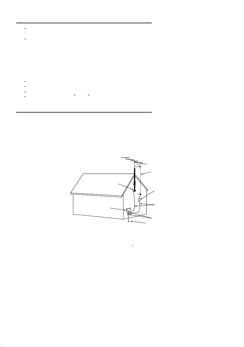
15.1. If an outside antenna is connected to the television set, be sure the antenna system is grounded so as to provide some
protection against voltage surges and built up static charges, Section 810 of the National Electrical Code, NFPA No.
70-1975, provides information with respect to proper grounding of the mast and supporting structure, grounding of the
lead-in wire to an antenna discharge unit, size of grounding conductors, location of antenna discharge unit, connection
to grounding electrode, and requirements for the grounding electrode.
EXAMPLE OF ANTENNA GROUNDING AS PER NATIONAL ELECTRICAL CODE INSTRUCTIONS
EXAMPLE OF ANTENNA GROUNDING AS PER
NATIONALELECTRICAL CODE
ANTENNA
LEAD- INWIRE
GROUND CLAMP
ELECTRIC SERVICE
EQUIPMENT
NEC-NATIONALELECTRICAL CODE
ANTENNA DISCHARGE
UNIT (NEC SECTION
810-20)
GROUNDING
CONDUCTORS
(NECSECTION 810-21)
GROUND CLAMPS
POWER SERVICE GROUNDING
ELECTRODE SYSTEM
(NEC ART 250. PARTH)
15.2. Note to CATV system installer : (Only for the television set with CATV reception)
This reminder is provided to call the CATV system attention to Article 820-40 of the NEC that provides
installer s
guidelines for proper grounding and, in particular, specifies that the cable ground shall be connected to the grounding
system of the building, as close to the point of cable entry as practical.
16. An outside antenna system should not be located in the vicinity of overhead power lines or other electric lights or power
circuits, or where it can fall into such power lines or circuits. When installing an outside antenna system, extreme care
should be taken to keep from touching such power lines or circuits as contact with them might be fatal.
17. For added protection for this television set during a lightning storm, or when it is left unattended and unused for long
periods of time, unplug it from the wall outlet and disconnect the antenna. This will prevent damage due to lightning
and power-line surges.
4
Page 5

OPERATION OF YOUR SET
18.
This television set should be operated only from the type of power source indicated on the marking label. If you are not
sure of the type of power supply at your home, consult your television dealer or local power company. For television
sets designed to operate from batter y power, refer to the operating instructions.
19. If the television set does not operate normally by following the operating instructions, unplug this television set from the
wall outlet and refer servicing to qualified service personnel. Adjust only those controls that are covered in the operating
instructions as improper adjustment of other controls may result in damage and will often require extensive work by a
qualified technician to restore the television set to normal operation.
20. When going on a holiday : If your television set is to remain unused for a period of time, for instance, when you go on
a holiday, turn the television set and unplug the television set from the wall outlet.
off
IF THE SET DOES NOT OPERATE PROPERLY
21. If you are unable to restore normal operation by following the detailed procedure in your operating instructions,
do not attempt any further adjustment. Unplug the set and call your dealer or service technician.
22. Whenever the television set is damaged or fails, or a distinct change in performance indicates a need for
service, unplug the set and have it checked by a professional service technician.
23. It is normal for some TV sets to make occasional snapping or popping sounds, particularly when being
turned on or off. If the snapping or popping is continuous or frequent, unplug the set and consult your
dealer or service technician.
FOR SERVICE AND MODIFICATION
24. Do not use attachments not recommended by the television set manufacturer as they may cause hazards.
25. When replacement parts are required, be sure the service technician has used replacement parts specified
by the manufacturer that have the same characteristics as the original part. Unauthorized substitutions
may result in fire, electric shock, or other hazards.
26. Upon completion of any service or repairs to the television set, ask the service technician to perform
routine safety checks to determine that the television is in safe operating condition.
5
Page 6

2、Specification
Chassis
Target Market
CRT
Color System
(TV)
Sound System
(TV)
Sound System
(TV)
System (AV)
Power Supply
Standby
picture
Terminal Rear RCA x *
matching CRT size 21" 21"
Slim CRT
PAL
PAL(BG DK I)
PAL(M N)
SECAM
NTSC
D/K
B/G
I
M
M/N
Global NICAM
German Stereo
BTSC
Sound effect
Woofer
Teletext
V-chip/ CCD
MONO(AV)
STEREO(AV)
PAL
PAL(M N)
NTSC
SECAM
AC 90-240V, 50/60Hz
AC 180-240V, 50/60Hz
AC 160-240V, 50/60Hz
AC 110, 50/60Hz
AC108V-132V 50/60Hz
<1W
<3W
<4W
<6W
<9W
<10W
<12W
Comb-f for NTSC (1H delay)
Comb-f for PAL/NTSC (4/2H
delay)
Rear SCART(Single)
S-Video (Rear or Side)
SY33 SY33
S.America APAC/Russia
√√
★√
√
★√
√
★√
★√
★√
√
√
★√
★√(2for1)
√√
√√
AC90-270V AC90-270V
√√
√(built-in MCU) √(built-in MCU)
★2 input/ 1output ★2 input/ 1output
★√ ★√
★√(2for1)
Page 7

YPbPr
HDMI
Language
digital module DVB-T / ATSC
★√ ★√
English/Portuguese/French/ Spanish
(1)English/Russian/Arabic;
(2)English/Vietnamese/Thai;★
Thai Bilingual
Page 8

3、Alignment Procedure
Method for Entering Factory Mode:
a. Production mode: Press the key [Fac] in remote control to enter or exit factory mode(But only
display 4 pages);
b. Engineer mode: Press key [DISPLAY] to display channel information(Setup for display picture
on bottom left of screen, press the number key [6][1][5][8] ;
c. Display “--PRODUCT--”,then press the key [MUTE] two times,the factory menu on the screen 。
The number on top right corner of factory menu is page number of factory menu. Press the key
[CH+/-] to adjust curser up or down。Press the key [VOL+/-] to change the value。When choose
the first top line, press [VOL+] / [VOL-] to choose the menu page。
d. Press key [sleep] to display factory menu in production mode. Please choose next page when display
factory menu。
e. Press key [0] to be shifted to one bright line status in production mode,. Press key [0] again to return factory
menu.
Relevant key number for one bright line:
[1] RB+ [2] GB+ [3] BB+
[4] RB- [5] GB- [6] BB-
Factory Service Menu Index:
*** PAGE 1 ****** Init Range
V.POSITION/50 19 0…63
V.POS SHIFT/50 0 0…15
V.SIZE/50 79 0…127
V.LIN/50 23 0…31
V.SC 17 0…31
OSD-V-START/50 0 0…3
OSD-H-POS 20 0…127
CHANGE PRO.
*** PAGE 1 ****** Init Range
V.POSITION/60 19 0…63
V.POS SHIFT/60 0 0…15
V.SIZE/60 79 0…127
V.LIN/60 23 0…31
V.SC 17 0…31
OSD V.START/60 0 0…3
OSD-H-POS 20 0…127
CHANGE PRO.
*** PAGE 2 ****** Init Range
H.PHASE/50 15 0…31
Page 9

H-BLK L 0 0…7
H-BLK R 3 0…7
H-SIZE 0…63
H.SIZE COMP/50 0…7
TRAPE/50 0…63
PARABOLAO/50 0…63
U.CORNER TOP/50 0…15
U.CORNER BTM/50,60 0…15
*** PAGE 2 ****** Init Range
H.PHASE/60 15 0…31
H-BLK L 0 0…7
H-BLK R 3 0…7
H-SIZE 0…63
H.SIZE COMP/60 0…7
TRAPE/60 0…63
PARABOLAO/60 0…63
U.CORNER TOP/60 0…15
U.CORNER BTM/60 0…15
*** PAGE 3 ****** Init Range
RB 127 0…255
GB 127 0…255
BB 127 0…255
R-D 90 0…127
G-D 12 0…15
B-D 90 0…127
S.B 80 0…127
*** PAGE 4 ****** Init Range
PROD.AGING OFF OFF/ON
RF-AGC-DELAY 16 0…63
CONTRAST/50 60 0…63
COLOR/50 20 0…63
SHARP/50 8 0…31
TINT/00 30 0…63
EW-COR.SW 1 0/1
CLEAR INFO NO NO/YES
*** PAGE 5 ****** Init Range
OSD CON. 3 0…7
FULL-OSD CON. 2 0…7
OPT-AV 2 0…3
Page 10

OPT-SVIDEO YES NO/YES
OPT-DVD YES NO/YES
OPT-AV3 NO NO/YES
AMERICA N/S USA/(N/S)
TUNE-SPEED 3 0…3
CH6 BAND 0 0/1
*** PAGE 6 ****** Init Range
OSD THEME 0 0…7
OPT-LOGO 0 0/1
HALF TONE 1 0…3
*** PAGE 7 ***CHROMA Init Range
COL-AUTO ON ON/OFF
COL-NTSC ON ON/OFF
COL-PAL/M ON ON/OFF
COL-PAL/N ON ON/OFF
C.TRAP ADJ/PAL 7 0…7
C.TRAP ADJ/NTSC 4 0…7
C.BPF ADJ. 0 0…3
C.VCO ADJ/NTSC
*** PAGE 8 ***FM Init Range
DEEM.TC 1 0/1
FM.GAIN
4 0…7
0 0/1
INIT EEPROM
*** PAGE 9 ***Other Init Range
PRO.MUTE OFF ON/OFF
BRI.MAX 63 0…63
VOL/01 0 0…127
VOL/16 61 0…127
VOL/36 103 0…127
*** PAGE 10 ***ON/OFF Init Range
AC-POWER ON LAST LAST/OFF
ON-TV/AV LAST TV/LAST
ON-DELAY 1 0…3
ON-SEARCH NO YES/NO
OFF-V.DELAY 0…7
NO YES/NO
Page 11

*** PAGE 11 ***PIC. Init Range
BLK.STR.START
BLK.STR.GAIN 3 0…3
*** PAGE 12 ***PIC. Init Range
BRT.ABL.DEF 1 0/1
MID.STP.DEF 1 0/1
BRT.ABL.TH 7 0…7
CORING GAIN 0 0…3
WPL OPE.POINT 2 0…3
Y GAMMA 2 0…3
DC.REST
COL.KILLER OPE. 4 0…7
RGB TEMP SW 1 0/1
*** PAGE 13 ***PIC. Init Range
SH ADJUST 0 0/1
B-Y/DC 12 0…15
R-Y/DC 12 0…15
B-Y/DC.DVD 9 0…15
R-Y/DC.DVD 9 0…15
*** PAGE 14 ***SYNC. Init Range
AFC GAIN/GATE 1 0/1
FBPBLK.SW 1 0/1
VSEPUP 0 0/1
VBLK SW 0 0/1
V.COUNT AUTO YES YES/NO
V.COMP 3 0…7
SYNC.SEP.S 4 0…7
H.FREQ/ES 32 0…63
VCO FREQ.IF/ES
*** PAGE 15 ***C.DEMO Init Range
G-Y AMP 8 0…15
G-Y ANGLE 0 0/1
R/B GAIN 8 0…15
R/B ANGLE 8 0…15
PAL APC SW 0 0/1
OPT-V.PROTECT OFF OFF/ON
V.PROTECT TH.
0 0…3
2 0…3
31 0…31
Page 12

OPT-ABL.P OFF OFF/ON
ABL-LOW LIMIT 63 0…63
*** PAGE 16 ***IF Init Range
OVER.MOD.SW OFF OFF/ON
OVER.MOD.LEVEL 2 0…15
PRE-SHOOT ADJ 0 0…3
OVER-SHOOT ADJ 0 0…3
VIDEO LEVEL 7 0…7
VIDEO.LVL.OFFSET 2 0…3
S.TRAP ADJ 4 0…7
IF VCO ADJ 2 0…3
Page 13
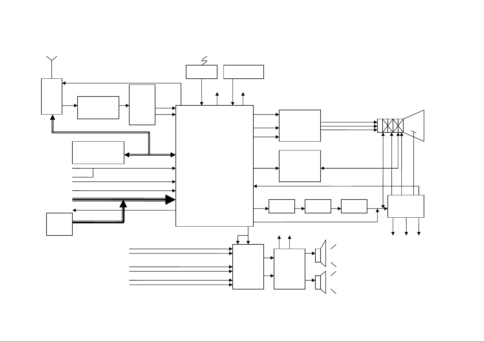
4、Block Diagram
Antenna
AGC
IR1001 Key Board
Tuner
AV1
S V ideo Y
AV2
YCbCr
AV out
Scart
signal
Q101 IF
Preamplifier
IC001
24C16 EEPROM
C
Scart Audio
AV1 Audio
R/L
AV2 Audio
R/L
R/L
Z101
SAW
LBN3
383
48 49 51
63
64
I2C BUS
31
32
46
45
54
MUTE
61
26 29 36 30
IC201
LA76933
IFamplifier/ Video detection
/Sound detectionj/ Y&C
Separation/ Color decode/
Base color matrix/ Sync
separation/ display process/
AV switch/ MCU/ OSD
52
STB BY
5
12
IC901
4052
Electron
Switch
12
13
14
Q502/Q504/
Q506 V i deo
Preamplifier
IC301
17
LA78041
V-amplifier
44
21
Q401 T401 Q402
15 EW
AV Audio out
3
13
IC601
LA4235
2 Audio
8
12
Amplifie
V SCAN
FBP
FOCUS
H SCAN
SCREEN
T402
FBT
4/5 11 10
±14V 220V 6.3V
HV
Page 14

5、Circuit Flow Introduction
1)、Chassis summarize
The main chip of SY33 chassis adopt IC LA76933 of SANYO company ,audio power
amplifier adopts IC LA42352,power supply adopts IC STRW6553, and vertical scan amplifier
adopts IC LA78041.The chassis has low cost and steady function, it has been adopts for
25M63,21M63 model.
2)、Base features
The unit TV supports PAL/DK.I,AV supports PAL/NTSC system, in 2XAV,1x S-video
3)、Unit Signal Flow Introduction
SY33 chassis circuit includes tuner, IF ,SAWF,LA76933 H/V scan circuit ,AV board, side AV
board, keypad board, USB board, power board. audio power amplifier circuit and power supply
circuit etc. The main ICs are LA78041,LA42352,HPC922-C,L7809CV,L7805CV, LA76933,
HCF4052 IC etc.
1)TV signal flow
RF from antenna enters tuner to be processed ( RF being inverted IF), and IF from pin11 of
TU101 passes R106 ,C110 to Q101 IF preamplifier .
After amplifying, IF signal enters pin1 of Z101 to filter and separate SIF and PIF via pin4 and
pin5 of Z101 into pin63 and pin64 of IC201(LA76933) to process PIF .
There are two ways output signal of process IF amplifier:
One is video signal, from pin60 of IC201 , after R227,R228 adjustment ,it is sent pin56 of
IC201 to process demodulation of picture.
Another way is sound signal, from pin5 of IC201 and passes C260 coupling。 The sound
signal is sent to pin1 and pin9 of IC901,after IC901 choosing, signal from pin3 and pin13 of
IC901 is sent to pin2 and pin4 of IC601 to process sound power amplification. After amplifying,
The signals from pin8 and pin12 of IC601 is sent to L/R speaker.
2) AV signal flow
AV1 signal process circuit.
Video signal of AV1from pin1 of P901 enters to pin46 of IC201 to decode process.
Sound signals of AV1from pin2 and pin3 of P901 input is sent to pin5 and pin 14 of IC901 to
choose , after being choosed, the signal flow same as TV sound.
AV2 signal process circuit.
Page 15

Video signal of AV2 from pin4of P901 is sent to pin54 of IC201 to decode process.
Sound signals of AV2 from pin5 and pin6 of P901 is sent to pin1 and pin 12 to choose
signal,.After being choosed, the signal flow same as TV sound.
3) High-Definition signal flow.
Y signal from pin7 of P901 enters pin48 of IC201 to process video.
Cb signa from pin8 of P901 enters pin49 of IC201 to process video.
Cr signal from pin9 of P901 enters pin51 of IC201 to process video.
4) Sound signal flow
Volume control:
Sound signal from pin27 and pin28 of IC201 enters pin6 and pin13 of IC601 to be amplified
and be sent out form pin8 and pin12 of IC601.
Mute control:
Pin30 of IC201 sends mute control signal, and passes D002 to connect base of Q602,controls
the Q602 ON or OFF, the pin C of Q602 connects pin5 of IC601 to control mute normal
working .When Q602 off, pin5 of IC601 is high level. So pin8 and pin12 of sound signal output
to speaker, when MCU sent mute signal of high level,Q602 ON, it lets the pin5 of IC601 is low
level to shut down the sound signal of pin8/pin12 of IC601, the mute is working.
TU101 is a common tuner. The RF signal is processed by tuner inside circuit disposal :high
frequency amplifier 、mixing、 high frequency demodulation、AGC、AFT、PLL。Then IF output
signal from pinIF of TU101 passes preamplifier Q101 to enter SAW Z101. The PIF signal from
pin4 and pin5 of Z101, enters pin63 and pin64 of IC201 to be decoded.
Page 16

N
6、Troubleshooting
LED ok,No Picture,
o sound
Check if 112V is short
to ground?
N
Check if 18V is short
to ground?
N
Check IC201 power
supply +5V ok?
Y
Check waveform of
X001ok?
Y
The waveform of
SDA and SCL ok?
Y
Check +5VA ok?
Y
The waveform of
H-out of IC 201 ok?
Y
Q401output
waveform ok?
Y
Q401output
waveform ok?
Y
Check each pin of
T402 ok?
Y
Check IC301 ok?
Y
Check ambient
parts of IC301
and replace the bad
N
N
N
N
N
N
N
N
Y
Replace Q402
Y
Replace IC601
Check which branch
N
short to ground and
repairing
Replace X001
Replace IC001
Replace IC205
Replace IC201
Replace Q401 or D406
Replace Q401
Replace T402
Replace IC301
Page 17

No LED,No Picture
Check
D801-D804,
RT801,C806
Replace
300V ok?
Y
Check
D801-d804,Q815
No Sound,Picture ok
Check which channel
no sound
Y
F801 ok?
N
N
Check Q815,
IC801 and
ambient parts
Replace
TV no sound AV no sound
Replace IC901
or repairing the
channel
N
IC 901sound output ok?
Y
Check IC601 or
ambient parts
Replace
Check pin5
of IC201
output ok?
N Y
Replace
IC201
Replace
C292 or
C260
Page 18

7ÿSchematic Diagram
Page 19

8ÿMain IC Introduction
LA769337X(X:J〜N)/LA769337FBTentative
1)
LA76933
Pin Assignment
PIN FUNCTION PIN FUNCTION PIN FUNCTION PAD Name
内部結線
Internal connections
1 SIF Output 64 VIF Input1 BIP
2 VIF AGC 63 VIF Input2 PInt01 C_Sync PSYNC P33
3 SIF Input 62 IF Ground PInt02 CLOCK PCL P32
4 FM Filter 61 RF AGC Output PInt03 DATA PDA P31
60 Video Output
Output
6 Audio Output 59 AFT Filter PInt06 INT_B PB B
7 SIF APC Filter 58 APC Filter PInt07 INT_G PG G
8 IF Vcc 57 Black Level Det. Filter PInt08 INT_R PR R
Ext. Audio Input / VM
Output
10 ABL 55 Video/Vertical Vcc PInt11 ENABLE PENA P30
11 RGB Vcc 54 External Video Input PInt12 PDC PPDC PEIN
12 Red Output 53 Chroma APC Filter PInt13 CVBS PCVBS CVIN
56 Internal Video Input
fsc Output
PInt04 I PI I 5 FM Output / Selected Audio
PInt05 FS PFS BL
PInt09 HS PHS HS 9
PInt10 VS PVS VS
PInt14 CPU TST B PCPUB TSTB 13 Green Output 52 Selected Video Output or
PInt15 CPU TST G PCPUG TSTG
μCOM
14 Blue Output 51 Cr Input PInt16 CPU TST R PCPUR TSTR
15
16 V Ramp Osc. Capacitor 49 Cb Input PInt18 AFT PAFT AN3
17 Vertical Output 48 DVD-Y PInt19 VDD PVDD VDDi
18 VCO IREF 47 NC Pint20 4MHZ
19 Horizontal/BUS Vcc 46 YC-Y Pint21 R out PROUT
20 Horizontal AFC Filter 45 YC-C Pint22 B out PBOUT
21 Horizontal Output 44 Flyback Pulse Input Pint23 Vref PVREF
22 Video/Vertical/BUS Ground 43 CCD Vcc
23 P00/INT0 42 CPU Ground Pint25 R input PR_IN
24 P01/INT1 41 FIL
25 P02 40 RES
26 P03/INT3 39 P07/AN7
27 P14/PWM1 38 P06/AN6
28 P15/PWM2 37 P05/AN5
E/W Output
50 4.43MHz Crystal PInt17 Reset PRES RESi
P4M
Clock
Pint24 B input PB_IN
Pint26 Vcc*2 PVCC2
29 P17 36 P04/AN4
30 P16/PWM3 35 VDD
31 P12/SDA1 34 XT2
32 P13/SCK1 33 XT1
No.72
Page 20

Page 21
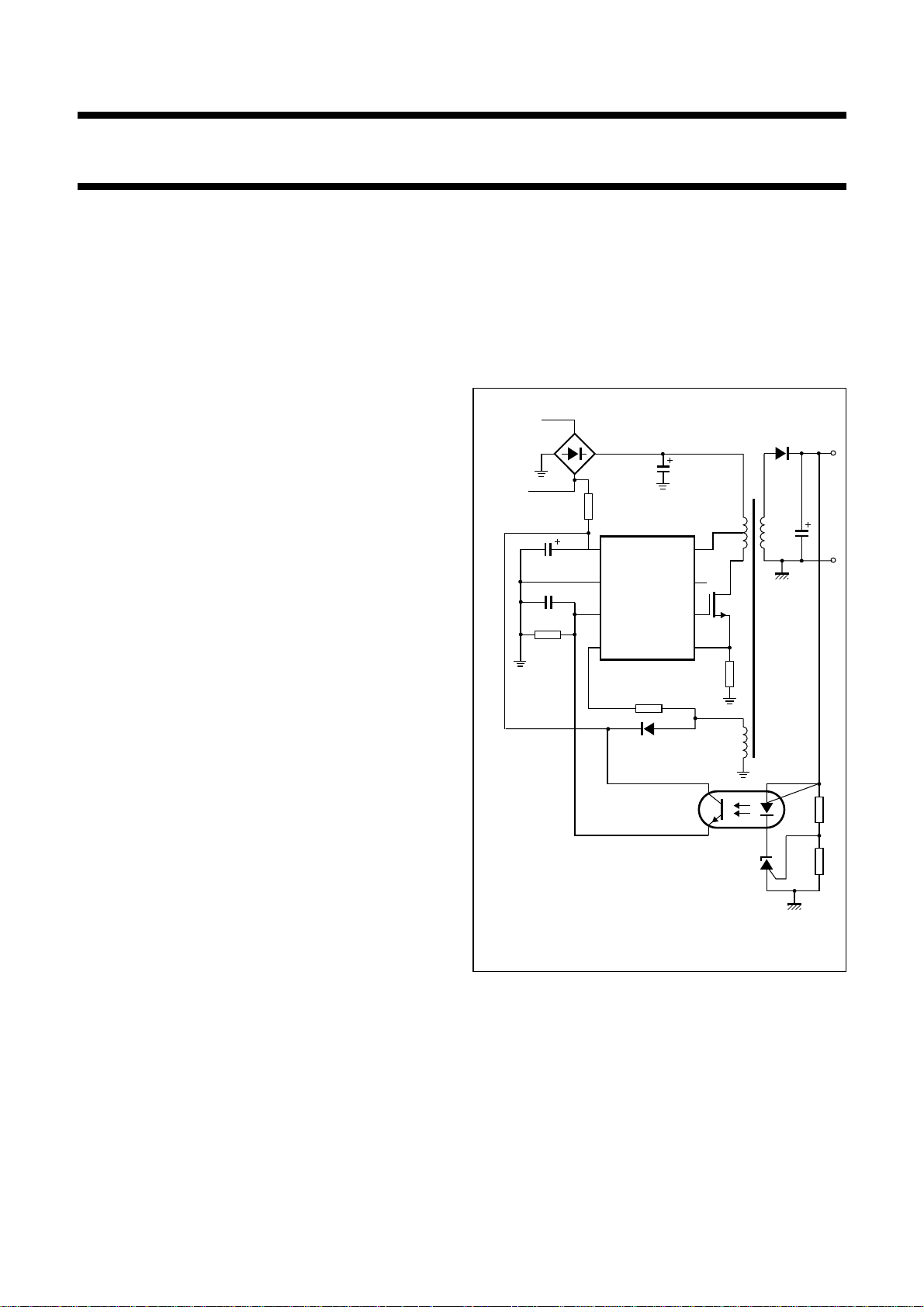
2ÿ
TEA1506
GreenChipII SMPS control IC
TEA1506P; TEA1506AP;
TEA1506T; TEA1506AT
FEATURES
Distinctive features
• Universal mains supply operation (70 to 276 V AC)
• High level of integration; giving a low external
component count.
Green features
• Valley or zero voltage switching for minimum switching
losses
• Efficient quasi-resonant operation at high power levels
• Frequency reduction at low power standby for improved
system efficiency (≤3W)
• Cycle skipping mode at very low loads.
Protection features
• Safe restart mode for system fault conditions
• Continuous mode protection by means of
demagnetization detection (zero switch-on current)
• Accurateandadjustableovervoltage protection (latched
in TEA1506; safe restart in TEA1506A)
• Short winding protection
• Undervoltage protection (foldback during overload)
• Overtemperature protection
• Low and adjustable overcurrent protection trip level
• Soft (re)start.
APPLICATIONS
Besides typical application areas, i.e. TV and monitor
supplies, the device can be used in adapters and chargers
and all applications that demand an efficient and
cost-effective solution up to 150 W. Unlike the other
GreenChipII control ICs, the TEA1506 has no internal
high voltage start-up source and needs to be started by
means of an external bleeder resistor.
1
2
TEA1506P
TEA1506AP
3
4
8
7
6
5
2003 Sep 09 2
MDB504
Fig.1 Basic application diagram.
Page 22

This text is here in white to force landscape pages to be rotated correctly when browsing through the pdf in the Acrobat reader.This text is here in
k
_white to force landscape pages to be rotated correctly when browsing through the pdf in the Acrobat reader.This text is here inThis text is here in
white to force landscape pages to be rotated correctly when browsing through the pdf in the Acrobat reader. white to force landscape pages to be ...
2003 Sep 09 4
, full pagewidth
BLOCK DIAGRAM
Philips Semiconductors Product specification
GreenChipII SMPS control IC
V
CC
GND
CTRL
1
(2)
2
(3)
3
(6)
I
prot(CTRL)
3.8 V
−1
SUPPLY
MANAGEMENT
internal
FREQUENCY
UVLO start
supply
VOLTAGE
CONTROLLED
OSCILLATOR
CONTROL
POWER-ON
RESET
OVER-
TEMPERATURE
PROTECTION
UVLO
V
< 4.5 V
CC
or UVLO
(TEA1506AT)
LOGIC
UP/DOWN
COUNTER
LOGIC
SQ
R
Q
SQ
R
Q
100
mV
VALLEY
OVER-
VOLTAGE
PROTECTION
DRIVER
LEB
blank
OCP
I
prot(DEM)
clamp
soft
start
S2
8
DRAIN
(14)
4
DEM
(7)
6
DRIVER
(11)
I
ss
0.5 V
5
I
sense
(9)
TEA1506P; TEA1506AP;
TEA1506T; TEA1506AT
TEA1506P;
TEA1506AP
(TEA1506T;
TEA1506 AT)
Pin numbers in parenthesis represent the SO version.
MAXIMUM
ON-TIME
PROTECTION
Fig.2 Block diagram.
short
winding
0.88 V
OVERPOWER
PROTECTION
MDB505
Page 23

Philips Semiconductors Product specification
GreenChipII SMPS control IC
TEA1506P; TEA1506AP;
TEA1506T; TEA1506AT
PINNING
SYMBOL
V
CC
GND 2 3 ground
CTRL 3 6 control input
DEM 4 7 input from auxiliary winding for demagnetization timing; overvoltage and
I
sense
DRIVER 6 11 gate driver output
HVS 7 12, 13 high voltage safety spacer; not connected
DRAIN 8 14 drain of external MOS switch; input for valley sensing and initial internal
n.c. − 1, 4, 5, 8,10not connected
PIN
DESCRIPTION
DIP8 SO14
1 2 supply voltage
overpower protection
5 9 programmable current sense input
supply
handbook, halfpage
V
CC
GND
CTRL
DEM
1
2
TEA1506P
TEA1506AP
3
4
MDB506
8
7
6
5
DRAIN
HVS
DRIVER
I
sense
Fig.3 Pin configuration DIP8.
handbook, halfpage
n.c.
V
CC
GND
n.c.
n.c.
CTRL
DEM
1
2
3
4
TEA1506AT
5
6
7
TEA1506T
MDB507
14
13
12
11
10
9
8
DRAIN
HVS
HVS
DRIVER
n.c.
I
sense
n.c.
Fig.4 Pin configuration SO14.
2003 Sep 09 5
Page 24

Philips Semiconductors Product specification
GreenChipII SMPS control IC
FUNCTIONAL DESCRIPTION
The TEA1506 is the controller of a compact flyback
converter, and is situated at the primary side. An auxiliary
winding of the transformer provides demagnetization
detection and powers the IC after start-up.
The TEA1506 can operate in multi modes (see Fig.5).
handbook, halfpage
(kHz)
f
VCO fixed quasi resonant
175
25
Fig.5 Multi modes operation.
MGU508
P (W)
TEA1506P; TEA1506AP;
TEA1506T; TEA1506AT
V
handbook, halfpage
sense(max)
Fig.6 V
0.52 V
sense(max)
1 V
(typ)
1.5 V
(typ)
voltage as function of V
The moment the voltage on pin VCC drops below the
undervoltage lock-out level, the IC stops switching and
re-enters the safe restart mode.
Supply management
MGU233
V
CTRL
CTRL
.
The next converter stroke is started only after
demagnetization of the transformer current (zero current
switching), while the drain voltage has reached the lowest
voltage to prevent switching losses (green function). The
primary resonant circuit of the primary inductance and
draincapacitor ensures this quasi-resonant operation. The
design can be optimized in such a way that zero voltage
switching can be reached over almost the universal mains
range.
To prevent very high frequency operation at lower loads,
the quasi-resonant operation changes smoothly in fixed
frequency PWM control.
At very low power (standby) levels, the frequency is
controlled down, via the VCO, to a minimum frequency of
approximately 25 kHz.
Start-up and undervoltage lock-out
Initially the IC is in the save restart mode. As long as V
is below the V
level, the supply current is nearly
CC(start)
CC
zero.
TheICwillactivatethe converter as soon as the voltage on
pin VCC passes the V
CC(start)
level.
The IC supply is taken over by the auxiliary winding as
soon as the output voltage reaches its intended level.
All (internal) reference voltages are derived from a
temperature compensated, on-chip band gap circuit.
Current mode control
Current mode control is used for its good line regulation
behaviour.
The ‘on-time’ is controlled by the internally inverted control
voltage, which is compared with the primary current
information. The primary current is sensed across an
external resistor. The driver output is latched in the logic,
preventing multiple switch-on.
The internal control voltage is inversely proportional to the
external control pin voltage, with an offset of 1.5 V. This
means that a voltage range from 1 to 1.5 V on pin CTRL
will result in an internal control voltage range from
0.5 to 0 V (a high external control voltage results in a low
duty cycle).
Oscillator
The maximum fixed frequency of the oscillator is set by an
internal current source and capacitor. The maximum
frequency is reduced once the control voltage enters the
VCO control window. Then, the maximum frequency
changeslinearly with the control voltageuntil the minimum
frequency is reached (see Figs 6 and 7).
2003 Sep 09 6
Page 25

Philips Semiconductors Product specification
GreenChipII SMPS control IC
handbook, halfpage
f
(kHz)
175
25
VCO
VCO
2
level
level
Fig.7 VCO frequency as function of V
handbook, full pagewidth
1
MGU509
175 kHz
V
sense(max) (V)
sense(max)
TEA1506P; TEA1506AP;
TEA1506T; TEA1506AT
Cycle skipping
At very low power levels, a cycle skipping mode will be
activated. A high control voltage will reduce the switching
frequency to a minimum of 25 kHz. If the voltage on the
control pin is raised even more, switch-on of the external
power MOSFET will be inhibited until the voltage on the
control pin has dropped to a lower value again (see Fig.8).
For system accuracy, it is not the absolute voltage on the
control pin that will trigger the cycle skipping mode, but a
signal derived from the internal VCO will be used.
Remark: If the no-load requirement of the system is such
.
that the output voltage can be regulated to its intended
level at a switching frequency of 25 kHz or above, the
cycle skipping mode will not be activated.
f
osc
1.5 V − V
CTRL
CTRL
X2
V
x
150 mV
The voltage levels dV1 and dV2 are fixed in the IC to 50 mV (typical) and 18 mV (typical) respectively.
current
comparator
V
I
DRIVER
OSCILLATOR
DRIVER
I
sense
f
max
f
min
cycle
skipping
1
0
Fig.8 The cycle skipping circuitry.
dV
2
dV
1
150
Vx (mV)
MGU510
Vx (mV)
2003 Sep 09 7
Page 26

Philips Semiconductors Product specification
GreenChipII SMPS control IC
Demagnetization
The system will be in discontinuous conduction mode all
the time. The oscillator will not start a new primary stroke
until the secondary stroke has ended.
Demagnetization features a cycle-by-cycle output
short-circuit protection by immediately lowering the
frequency (longer off-time), thereby reducing the power
level.
Demagnetizationrecognition is suppressed during the first
t
time. This suppression may be necessary in
suppr
applications where the transformer has a large leakage
inductance, at low output voltages and at start-up.
If pin DEM is open-circuit or not connected, a fault
condition is assumed and the converter will stop operating
immediately. Operation will recommence as soon as the
fault condition is removed.
Minimum and maximum ‘on-time’
The minimum ‘on-time’ of the SMPS is determined by the
Leading Edge Blanking (LEB) time. The IC limits the
‘on-time’ to 50 µs. When the system desires an ‘on-time’
longer than 50 µs, a fault condition is assumed (e.g.
removed Ciin Fig.12), the IC will stop switching and enter
the safe restart mode.
TEA1506P; TEA1506AP;
TEA1506T; TEA1506AT
Regarding the TEA1506, the IC will not start switching
again. Subsequently, VCC will drop again to the UVLO
level, etc.
Operation only recommences when the VCCvoltage drops
below a level of about 4.5 V.
RegardingtheTEA1506A, when the V
switching starts again (safe restart mode) when the V
level is reached. This process is repeated as long as the
OVP condition exists.
Theoutput voltage V
atwhich the OVP function trips,
o(OVP)
can be set by the demagnetization resistor, R
V
N
----------N
=
o OVP()
s
I
(OVP)(DEM)RDEM
aux
× V
+{}
clamp(DEM)(pos)
where Nsis the number of secondary turns and N
number of auxiliary turns of the transformer.
Current I
(OVP)(DEM)
The value of R
is internally trimmed.
can be adjusted to the turns ratio of the
DEM
transformer, thus making an accurate OVP possible.
levelisreached,
start
DEM
:
aux
start
is the
OverVoltage Protection (OVP)
An OVP mode is implemented in the GreenChip series.
This works for the TEA1506 by sensing the auxiliary
voltage via the current flowing into pin DEM during the
secondary stroke. The auxiliary winding voltage is a
well-defined replica of the output voltage. Any voltage
spikes are averaged by an internal filter.
Iftheoutput voltage exceeds the OVP trip level, an internal
counter starts counting subsequent OVP events. The
counter has been added to prevent incorrect OVP
detections which might occur during ESD or lightning
events. If the output voltage exceeds the OVP trip level a
fewtimes and not again ina subsequent cycle, the internal
counter will count down with twice the speed compared
with counting-up. However, when typical 10 cycles of
subsequent OVP events are detected, the IC assumes a
true OVP and the OVP circuit switches the power
MOSFET off. Next, the controller waits until the UVLO
level is reached on pin VCC. When VCC drops to UVLO,
capacitor C
will be recharged to the V
VCC
start
level.
2003 Sep 09 8
Page 27

Philips Semiconductors Product specification
GreenChipII SMPS control IC
Valley switching
A new cycle starts when the power MOSFET is switched
on (see Fig.9). After the ‘on-time’ (which is determined by
the ‘sense’ voltage and the internal control voltage), the
switchis opened and the secondary stroke starts.After the
secondary stroke, the drain voltage shows an oscillation
primary
stroke
1
pCd
×()×
secondary
stroke
with a frequency of approximately
----------------------------------------------2 π× L
where L
is the primary self inductance of the transformer
p
and Cd is the capacitance on the drain node.
As soon as the oscillator voltage is high again and the
secondary stroke has ended, the circuit waits for the
handbook, full pagewidth
TEA1506P; TEA1506AP;
TEA1506T; TEA1506AT
lowest drain voltage before starting a new primary stroke.
This method is called valley detection.
Figure 9 shows the drain voltage together with the valley
signal, the signal indicating the secondary stroke and the
oscillator signal.
In an optimum design, the reflected secondary voltage on
the primary side will force the drain voltage to zero. Thus,
zero voltage switching is very possible, preventing large
1
P
capacitive switching losses
-- -
2
and allowing high frequency operation, which results in
small and cost effective inductors.
secondary
ringing
2
CV
× f××=
drain
valley
secondary
stroke
oscillator
BA
MGU235
A: Start of new cycle at lowest drain voltage.
B: Start of new cycle in a classical PWM system at high drain voltage.
Fig.9 Signals for valley switching.
2003 Sep 09 9
Page 28

Philips Semiconductors Product specification
GreenChipII SMPS control IC
MGU236
handbook, halfpage
−100 µA
(typ)
I
DEM
−24 µA
(typ)
Fig.10 OPP correction curve.
OverCurrent Protection (OCP)
The cycle-by-cycle peak drain current limit circuit uses the
externalsourceresistor to measure the current accurately.
This allows optimum size determination of the transformer
core (cost issue). The circuit is activated after the leading
edge blanking time, t
. The OCP circuit limits the ‘sense’
leb
voltage to an internal level.
V
sense(max)
0.52 V
(typ)
0.3 V
(typ)
TEA1506P; TEA1506AP;
TEA1506T; TEA1506AT
Short winding protection
After the leading edge blanking time, the short winding
protection circuit is activated. If the ‘sense’ voltage
exceeds the short winding protection voltage V
converter will stop switching. Once VCC drops below the
UVLO level, capacitor C
will be recharged and the
VCC
supply will restart again. This cycle will be repeated until
the short-circuit is removed (safe restart mode).
The short winding protection will also protect in case of a
secondary diode short-circuit.
OverTemperature Protection (OTP)
An accurate temperature protection is provided in the
circuit. When the junction temperature exceeds the
thermal shutdown temperature, the IC will enter the safe
restart mode.
When the V
level is reached, switching starts again.
start
This process is repeated as long as the OTP condition
exists.
swp
, the
OverPower Protection (OPP)
Duringthe primary stroke, the rectifiedmains input voltage
is measured by sensing the current drawn from pin DEM.
This current is dependent on the mains voltage, according
to the following formula:
N
where:
N
=
-----------N
aux
p
I
V
≈≈
-------------- -
DEM
R
DEM
aux
×
NV
mains
-------------------------R
DEM
The current information is used to adjust the peak drain
current, which is measured via pin I
. The internal
sense
compensation is such that an almost mains independent
maximum output power can be realized.
The OPP curve is given in Fig.10.
2003 Sep 09 10
Page 29

Philips Semiconductors Product specification
GreenChipII SMPS control IC
Control pin protection
If pin CTRL is open-circuit or not connected, a fault
conditionisassumed and the converter will stop switching.
Operation will recommence as soon as the fault condition
is removed.
Soft start-up
To prevent transformer rattle during hiccup, the
transformer peak current is slowly increased by the soft
start function. This can be achieved by inserting a resistor
and a capacitor between pin I
(see Fig.11). An internal current source charges the
capacitor to V = ISS× RSS, with a maximum of
approximately 0.5 V.
The start level and the time constant of the increasing
primary current level can be adjusted externally by
changing the values of RSS and CSS.
V
I
primary(max)
τ R
SSCSS
ocpISSRSS
=
---------------------------------------------- -
×=
The charging current I
pin I
pin I
is below approximately 0.5 V. If the voltage on
sense
exceeds 0.5 V, the soft start current source will
sense
×()–
R
sense
will flow as long as the voltage on
SS
start limiting the current ISS. At the V
current source is completely switched off.
Since the soft start current ISSis supplied from pin DRAIN,
the RSSvalue will not affect theVCCcurrent during start-up.
and the sense resistor
sense
level, the I
CC(start)
SS
TEA1506P; TEA1506AP;
TEA1506T; TEA1506AT
handbook, halfpage
I
SS
0.5 V
Driver
The driver circuit to the gate of the power MOSFET has a
current sourcing capability of 135 mA typical anda current
sink capability of 560 mA typical. This permits fast turn-on
and turn-off of the power MOSFET for efficient operation.
A low driver source current has been chosen to limit the
∆V/∆t at switch-on. This reduces Electro Magnetic
Interference (EMI) and also limits the current spikes
across R
sense
.
start-up
R
I
sense
5
V
ocp
C
Fig.11 Soft start.
SS
SS
R
sense
MGU237
2003 Sep 09 11
Page 30

10、B0M List
t
MATERIAL CONCENTRATIVE BOM PRINT
MATERIAL NO.: 03-DM62SAB-SC60S
MATERIAL NAME: S21M62Q/CS-SY33-LA
Parent Child Description
03-DM62SAB-SC60S T6-016W31-A009XZ
T6-016W31-A009XZ 06-016W31-A009X
ASS'Y-REMOTE CONTROL BD
OF ARTEQU
REMOTE CONTROLLER
RC1663108
ty
1PC
1PC
Uni
BOM text
03-DM62SAB-SC60S T8-21RFLN-HF4AB ASS'Y - MATCH TUBE 1 PC
T8-21RFLN-HF4AB T8-21RFLN-FHF4AB ASS'Y - MATCH TUBE(F.CAB) 1 PC
T8-21RFLN-FHF4AB 44-21RFLN-HF4A CRT A51ERS357X440 1 PC
T8-21RFLN-FHF4AB 46-27688H-04XG
T8-21RFLN-HF4AB T8-21RFLN-MHF4AB
HS 4P A/B 400/13 RBGW
TJC1/4Y
ASS'Y - MATCH TUBE(MAIN
BD)
1 PC FOR DY COIL
1PC
T8-21RFLN-MHF4AB 10-0BY228-F0X DIODE BY228 1 PC D405
T8-21RFLN-MHF4AB 10-0FR104-FBX
T8-21RFLN-MHF4AB 18-FG0151-JHX
T8-21RFLN-MHF4AB 18-FG0439-JHX
T8-21RFLN-MHF4AB 25-BCB101-M1X
T8-21RFLN-MHF4AB 27-AHQ393-JSX
T8-21RFLN-MHF4AB 27-AHR394-JSX
T8-21RFLN-MHF4AB 27-ALQ102-J0X
T8-21RFLN-MHF4AB 27-ALQ272-J0X
T8-21RFLN-MHF4AB 27-ALR133-J0X
T8-21RFLN-MHF4AB 36-LIN180-XX1
DIODE FR104 (FAST
RECTIFIER)
RES. M.O. 150 OHM 2W +/5%
RES. M.O. 4.3 OHM 2W +/5%
CAP. ELEC 100 UF 16V +/20%
CAP. M.PP 0.039 UF 400V
+/-5%
CAP. M.PP 0.39 UF 400V
+/-5%
CAP. M.PP 0.001UF 1.6KV
+/-5%
CAP. M.PP 0.0027UF 1.6KV
+/-5%
CAP. M.PP 0.013 UF 1.6KV
+/-5%
TCL36-LIN180-XX1= COIL
LINEARITY 18 UH R
1 PC D407
1 PC R318
1 PC R412
1 PC C275
1 PC C403
1 PC C421
1 PC C421A
1 PC C402
1 PC C406
1 PC L412
T8-21RFLN-MHF4AB 36-WID601-XX1 COIL CHOKE 600 UH 1 PC L411A
T8-21RFLN-MHF4AB 37-FCA001-EAA0A FLYBACK BSC27-0101Q 1 PC T402
T8-21RFLN-MHF4AB 66-343730-0B0
HOLLOW RIVET
1.6MMX3.0MMX3.2MM
2 PC FOR L411A
T8-21RFLN-HF4AB T8-DM62SAB-CRY ASS'Y - CRT BD 1 PC
T8-DM62SAB-CRY 10-1N4148-ABX DIODE 1N4148 (SWITCHING) 3 PC
T8-DM62SAB-CRY 11-SA1015-YBX
TRANSISTOR ST2SA1015Y
(PNP)
1 PC Q507
D207;D501;D
502
Page 31

T8-DM62SAB-CRY 11-TC3207-0BX TRANSISTOR KTC3207 3 PC
T8-DM62SAB-CRY 18-CB0101-JNX
T8-DM62SAB-CRY 18-CB0182-JNX
T8-DM62SAB-CRY 18-CB0332-JNX
T8-DM62SAB-CRY 18-CB0511-JNX
T8-DM62SAB-CRY 18-CB0681-JNX
T8-DM62SAB-CRY 18-CD0155-JNX
T8-DM62SAB-CRY 18-FE0272-JNX
T8-DM62SAB-CRY 18-FG0153-JHX
T8-DM62SAB-CRY 25-BCB101-M1X
T8-DM62SAB-CRY 25-BCB221-M1X
T8-DM62SAB-CRY 25-BLB109-M1X
T8-DM62SAB-CRY 26-ABC471-JZX
T8-DM62SAB-CRY 26-AMM681-KRX
T8-DM62SAB-CRY 26-EBP103-ZF1
T8-DM62SAB-CRY 26-EBP103-ZFS
T8-DM62SAB-CRY 35-139730-00X FERR. BEAD BF60 2 PC FOR C508
T8-DM62SAB-CRY 40-0Y12DG-CRB1XG P.C.B CRT BD 1 PC
T8-DM62SAB-CRY 46-10967W-01XG PIN BASE *1 TJC1-1A 1 PC P501
T8-DM62SAB-CRY 47-CRT004-XX0G
T8-DM62SAB-CRY 46-33079W-05XG PIN BASE *5 TJC3-5A 1 PC P503
T8-DM62SAB-CRY 46-35179W-04XG PIN BASE TJC3-4A 1 PC P502
03-DM62SAB-SC60S T8-DM62SAB-BSY ASS'Y - BASE 1 PC
T8-DM62SAB-BSY 54-420800-000 RUBBER PAD 3 PC
T8-DM62SAB-BSY T8-DM62SAB-BSYZ ASS'Y - BASE(ART) 1 PC
T8-DM62SAB-BSYZ 62-444330-0CL1A BASE 1 PC
T8-DM62SAB-BSYZ 74-045035-50H PLASTIC BAG 1 PC
03-DM62SAB-SC60S T8-DM62SAB-FCN ASS'Y - FRONT CABINET 1 PC
RES. C.F. 100 OHM 1/6W
+/-5%
RES. C.F. 1.8K OHM 1/6W
+/-5%
RES. C.F. 3.3K OHM 1/6W
+/-5%
RES. C.F. 510 OHM 1/6W
+/-5%
RES. C.F. 680 OHM 1/6W
+/-5%
RES. C.F. 1.5M OHM 1/4W
+/-5%
RES. M.O. 2.7K OHM 1/2W
+/-5%
RES. M.O. 15K OHM 2W +/5%
CAP. ELEC 100 UF 16V +/20%
CAP. ELEC 220 UF 16V +/20%
TCL25-BLB109-M1X= CAP.
ELEC 1 UF 250V +/
CAP. CER 470 PF 50V +/-5%
SL
CAP. CER 680 PF 2KV +/10% R
CAP CER 50V 2.5MM 10nF 20%+80%
CAP.CER 10NF 50V +80% 20%
TCL47-CRT004-XX0G= CRT
SOCKET GZS10-2-10
3PC
1 PC R514
2 PC R515;R522
6PC
1 PC R509
1 PC R524
3PC
3PC
1 PC C507
1 PC C506
1 PC C504
3PC
1 PC C505
1 PC C508
1 PC C509
1 PC S501
Q504;Q502;Q
506
R510;R501;R
505
R513;R511;R
508;R506;R5
03;R502
R519;R520;R
521
R516;R517;R
518
C502;C501;C
503
Page 32

T8-DM62SAB-FCN 54-114002-00X
T8-DM62SAB-FCN 54-205140-000 SPACER CRT MOUNTING T=2MM 4 PC
T8-DM62SAB-FCN 54-314740-0X0
T8-DM62SAB-FCN 57-389890-000 WIRE MOUNTS 80MMX2.2MM 3 PC
T8-DM62SAB-FCN 62-227680-0UA
T8-DM62SAB-FCN 62-227680-1UA FBT BRACKET 1 PC
T8-DM62SAB-FCN 62-444320-0CL SALVER 1 PC
T8-DM62SAB-FCN 62-450560-0UN TRACKING_R 1 PC
T8-DM62SAB-FCN 62-450570-0UN TRACKING_L 1 PC
T8-DM62SAB-FCN 63-B30100-AB2G SCREW-ST 3MM 10MM 62 R=Y 1 PC
T8-DM62SAB-FCN 63-B40100-BT4G S/T SCREW B 4 X 10 3 PC
T8-DM62SAB-FCN 63-B40150-AB4G
T8-DM62SAB-FCN 63-W30100-AB4G S/T SCREW W 3 X 10 AB 3 PC
T8-DM62SAB-FCN 63-Z60250-AB4G S/T SCREW HA 6X25 4 PC
T8-DM62SAB-FCN 67-M44681-0E4 METAL PART 1 PC
T8-DM62SAB-FCN T8-DM62SAB-FCNZ
T8-DM62SAB-FCNZ 55-DM62FC-1CL1A FRONT CABINET 1 PC
T8-DM62SAB-FCNZ 56-DM62FB-0HA5O PUSH BUTTON 1 PC
T8-DM62SAB-FCNZ 56-DM62LE-0HC5Z LENS 1 PC
T8-DM62SAB-FCNZ 58-DM62FI-0UI1A INLAY PUSH BUTTON 1 PC
T8-DM62SAB-FCNZ 67-2960LG-0A09A LOGO 1 PC
T8-DM62SAB-FCN 41-GND021-LX0 ASS'Y-GND BRAID 21“CRT 1 PC
T8-DM62SAB-FCN 36-DEG210-BX3 DEGAUSSING COIL 2500MM 1 PC
T8-DM62SAB-FCN 67-X12668-0E0 SPRING CRT 6MMX40MMX0.5MM 1 PC
T8-DM62SAB-FCN 42-41208D-XX0G SPEAKER YDP412-1A 2 PC W601,W602
T8-DM62SAB-FCN 46-14026H-02XG
T8-DM62SAB-FCN 46-27250H-02XG
T8-DM62SAB-FCN 63-Z30120-AB4G S/T SCREW 3.0 X 12 4 PC
03-DM62SAB-SC60S T8-DM62SAB-MANSM ASS'Y - CHASSIS BD 1 PC
FELT TAPE
(360MMX19MMX0.3MM)
CRT FIBRE SHEET
(22MMX22MMX0.8MM)
BRACKET ABS-KINGFA 606
(UO)
SCREW-ST 4MM 15MM ISO 62
R=Y
ASS'Y - FRONT
CABINET(ART)
HS 2P 2468#22 570MM S112Y/7MM
HS 2P24 450/5 F/W TJC302H
6PC
12 PC
1PC
6PC
1PC
1PC
1PC
MTG
CRT&F.CAB
MTG
CHASSIN&CRT
;
MTG LENS
PCB & F.CAB
MTG ARMOR
PLATE&CHASS
IN
MTG CHASSIN
& F.CAB
MTG LENS &
F.CAB;MTG
BUTTON &
F.CAB
MTG CRT &
F.CAB
P602H FOR
M.BD P602
P601H FOR
M.BD P601
MTG SPK &
F.CAB
Page 33

T8-DM62SAB-MANSM T8-DM62SAB-IRY
T8-DM62SAB-IRY 02-IRR001-XX1
T8-DM62SAB-IRY 11-SC1815-YBX
T8-DM62SAB-IRY 14-LED03R-XX1 LED RED Φ3MM FO203 1 PC D1101
T8-DM62SAB-IRY 18-CB0152-JNX
T8-DM62SAB-IRY 18-CB0470-JNX
T8-DM62SAB-IRY 18-CB0472-JNX
T8-DM62SAB-IRY 25-HCB470-M1X
T8-DM62SAB-IRY 26-EBP104-ZFS
T8-DM62SAB-IRY 40-21M62S-IRB1XG P.C.B IR RECEIVE BD 1 PC
T8-DM62SAB-IRY 46-33079W-04XG PIN BASE *4 TJC3-4A 1 PC P1101
T8-DM62SAB-MANSM T8-DM62SAB-KEY ASS'Y - KEY BD 1 PC
T8-DM62SAB-KEY 18-CB0122-JNX
T8-DM62SAB-KEY 18-CB0123-JNX
T8-DM62SAB-KEY 18-CB0152-JNX
T8-DM62SAB-KEY 18-CB0302-JNX
T8-DM62SAB-KEY 18-CB0472-JNX
T8-DM62SAB-KEY 40-21V18S-KEC1XG P.C.B KEY BD 1 PC
T8-DM62SAB-KEY 46-27626W-02XG
T8-DM62SAB-KEY 48-TAC002-XX1 TACT SWITCH TSVB-3-D 7 PC
T8-DM62SAB-MANSM T8-DM62SAB-MAN ASS'Y - MAIN BD 1 PC
T8-DM62SAB-MAN 07-457FF5-NA8XG FS TUNER FSNA05T-4-E 1 PC TU101
T8-DM62SAB-MAN 10-0001H8-FBX DIODE 1H8 (FAST RECOVERY) 1 PC D809
T8-DM62SAB-MAN 10-0FR104-FBX
T8-DM62SAB-MAN 10-0RL255-EBX
T8-DM62SAB-MAN 10-0RU3AM-FBX
ASS'Y - INFRARED RECEIVE
BD
IR RECEIVER MODULE
HRM380017
TRANSISTOR 2SC1815-Y
(NPN)
RES. C.F. 1.5K OHM 1/6W
+/-5%
RES. C.F. 47 OHM 1/6W +/5%
CARBON RES. C.F. 4.7K OHM
1/6W +/-5%
CAP. ELEC 47 UF 16V +/20%
CAP. CER 0.1UF 50V +80%/20%
RES. C.F. 1.2K OHM 1/6W
+/-5%
RES. C.F. 12K OHM 1/6W
+/-5%
RES. C.F. 1.5K OHM 1/6W
+/-5%
RES. C.F. 3K OHM 1/6W +/5%
CARBON RES. C.F. 4.7K OHM
1/6W +/-5%
PIN BASE *2 TJC3-2A
(HORIZ)
DIODE FR104 (FAST
RECTIFIER)
DIODE RL255 OR
RL206(POWER RECTIFIER)
HIGH EFFICIENCY RECTIFIER
RU3AM
1PC
1 PC IR1101
1 PC Q1101
1 PC R1102
1 PC R1103
1 PC R1101
1 PC C1101
1 PC C1102
1 PC R1001
1 PC R1006
2 PC R1002;R1003
1 PC R1004
1 PC R1005
1 PC P1001
K1001;K1002
;K1003;K100
4;K1005;K10
06;K1007
D820;D403;D
5PC
4PC
1 PC D833
402;D401;D4
90
D802;D803;D
804;D801
Page 34

T8-DM62SAB-MAN 10-0RU3YX-FBX DIODE RU3YX 2 PC D830;D841
T8-DM62SAB-MAN 10-1N4001-EBX DIODE 1N4001 (RECTIFIER) 1 PC D301
T8-DM62SAB-MAN 10-1N4007-EBX DIODE IN4007 1 PC D816
D204;D206;D
819;D203;D2
02;D201;D84
0;D814;D210
T8-DM62SAB-MAN 10-1N4148-ABX DIODE 1N4148 (SWITCHING) 21 PC
T8-DM62SAB-MAN 10-79C18V-DBX DIODE ZENER 18V 1/2W 5% 1 PC D821
T8-DM62SAB-MAN 10-79C33V-DBX DIODE ZENER 33V 1/2W 5% 1 PC D101
T8-DM62SAB-MAN 10-79C8V2-DBX DIODE ZENER 8V2 1/2W 5% 1 PC D205
T8-DM62SAB-MAN 10-79C9V1-DBX DIODE ZENER 9V1 1/2W 5% 1 PC D404
T8-DM62SAB-MAN 10-HS5V1B-DBX DIODE 500MW 5.1HSB 1 PC D001
T8-DM62SAB-MAN 11-SA1015-YBX
T8-DM62SAB-MAN 11-DD1556-0AX TRANSISTOR 3DD1556 1 PC Q402
T8-DM62SAB-MAN 11-DD2603-RAX TRANSISTOR 3DD2603-R 1 PC Q470
T8-DM62SAB-MAN 11-C124ES-0BX
T8-DM62SAB-MAN 11-SC1815-YBX
T8-DM62SAB-MAN 11-SC2235-YAX TRANSISTOR 2SC2235-Y(NPN) 1 PC Q401
T8-DM62SAB-MAN 11-SC3779-DBX
T8-DM62SAB-MAN 11-SD2012-0CX TRANSISTOR 2SD2012 1 PC Q203
T8-DM62SAB-MAN 11-SK2645-0AX
T8-DM62SAB-MAN 13-000040-52P IC 4052 1 PC IC901
T8-DM62SAB-MAN 13-000TL4-31T IC TL431ACLP 1 PC IC803
T8-DM62SAB-MAN 13-00M24C-08P
T8-DM62SAB-MAN 13-0HPC92-2CP PHOTO COUPLER HPC922-C 1 PC IC802
T8-DM62SAB-MAN 13-0L7805-CVS +5V 1.5A IC L7805CV 1 PC IC205
T8-DM62SAB-MAN 13-0LA769-33P IC LA76933FLASH 1 PC IC201(CP)
T8-DM62SAB-MAN 13-LA4235-20S IC LA42352 1 PC IC601
T8-DM62SAB-MAN 13-STV817-2AS IC STV8172A 1 PC IC301
T8-DM62SAB-MAN 13-TEA150-6PP
T8-DM62SAB-MAN 18-CB0100-JNX
TRANSISTOR ST2SA1015Y
(PNP)
TRANSISTOR PDTC124ES
(NPN)
TRANSISTOR 2SC1815-Y
(NPN)
TRANSISTOR 2SC3779D (RF
AMPL)
TRANSISTOR 2SK2645-01MR
(POWER
IC EEPROM 8K M24C08
(WRITE)
TCL13-TEA150-6PP= IC
TEA1506P R=N
RES. C.F. 10 OHM 1/6W +/5%
4PC
1 PC Q602
7PC
1 PC Q101
1 PC Q815
1 PC IC001(CP)
1 PC IC801
1 PC R814
;D602;D211;
D302;D406;D
470;D306;D2
20;D862;D86
3;D601;D601
A;D603
Q208;Q471;Q
801;Q472
Q844;Q842;Q
841;Q802;Q2
02;Q922;Q30
6
Page 35

T8-DM62SAB-MAN 18-CB0101-JNX
T8-DM62SAB-MAN 18-CB0102-JNX
T8-DM62SAB-MAN 18-CB0103-JNX
T8-DM62SAB-MAN 18-CB0104-JNX
T8-DM62SAB-MAN 18-CB0105-JNX
T8-DM62SAB-MAN 18-CB0121-JNX
T8-DM62SAB-MAN 18-CB0122-JNX
T8-DM62SAB-MAN 18-CB0151-JNX
T8-DM62SAB-MAN 18-CB0181-JNX
T8-DM62SAB-MAN 18-CB0184-JNX
T8-DM62SAB-MAN 18-CB0220-JNX
T8-DM62SAB-MAN 18-CB0221-JNX
T8-DM62SAB-MAN 18-CB0222-JNX
T8-DM62SAB-MAN 18-CB0223-JNX
T8-DM62SAB-MAN 18-CB0229-JNX
T8-DM62SAB-MAN 18-CB0243-JNX
RES. C.F. 100 OHM 1/6W
+/-5%
RES. C.F. 1K OHM 1/6W +/5%
RES. C.F. 10K OHM 1/6W
+/-5%
RES. C.F. 100K OHM 1/6W
+/-5%
TCL18-CB0105-JNX= RES.
C.F. 1M OHM 1/6W
RES. C.F. 120 OHM 1/6W
+/-5%
RES. C.F. 1.2K OHM 1/6W
+/-5%
RES. C.F. 150 OHM 1/6W
+/-5%
RES. C.F. 180 OHM 1/6W
+/-5%
RES. C.F. 180K OHM 1/6W
+/-5%
RES. C.F. 22 OHM 1/6W +/5%
RES. C.F. 220 OHM 1/6W
+/-5%
RES. C.F. 2.2K OHM 1/6W
+/-5%
RES. C.F. 22K OHM 1/6W
+/-5%
RES. C.F. 2.2 OHM 1/6W
+/-5%
RES. C.F. 24K OHM 1/6W
+/-5%
R915;R274;R
8PC
13 PC
16 PC
5PC
1 PC R262
1 PC R253
1 PC R811
2 PC R109;R108
2 PC R217;R336
1 PC R213
2 PC R057;R058
3PC
5PC
6PC
2 PC R602;R603
2 PC R267;R268
916;R261;R2
03;R202;R20
1;R255
R923;R922;R
605;R475;R4
11;R221;R01
3;R020A;R10
7;R220;R620
;R860;J220
R006;R004;R
606;R003;R8
40;R851;R31
2;R017;R020
;R021;R205;
R311;R271;R
604;R316;R0
10
R031;R238;R
925;R924;R8
63
R106;R919;R
264
R222;R912;R
917;R918;R9
26
R841;R846;R
914;R927;R9
21;R913
Page 36

T8-DM62SAB-MAN 18-CB0272-JNX
T8-DM62SAB-MAN 18-CB0274-JNX
T8-DM62SAB-MAN 18-CB0302-JNX
T8-DM62SAB-MAN 18-CB0331-JNX
T8-DM62SAB-MAN 18-CB0332-JNX
T8-DM62SAB-MAN 18-CB0333-JNX
T8-DM62SAB-MAN 18-CB0334-JNX
T8-DM62SAB-MAN 18-CB0391-JNX
T8-DM62SAB-MAN 18-CB0392-JNX
T8-DM62SAB-MAN 18-CB0822-JNX
T8-DM62SAB-MAN 18-CB0394-JNX
T8-DM62SAB-MAN 18-CB0470-JNX
T8-DM62SAB-MAN 18-CB0471-JNX
T8-DM62SAB-MAN 18-CB0472-JNX
T8-DM62SAB-MAN 18-CB0473-JNX
T8-DM62SAB-MAN 18-CB0474-JNX
T8-DM62SAB-MAN 18-CB0514-JNX
T8-DM62SAB-MAN 18-CB0560-JNX
T8-DM62SAB-MAN 18-CB0561-JNX
T8-DM62SAB-MAN 18-CB0562-JNX
T8-DM62SAB-MAN 18-CB0682-JNX
T8-DM62SAB-MAN 18-CB0683-JNX
RES. C.F. 2.7K OHM 1/6W
+/-5%
TCL18-CB0274-JNX= RES.
C.F. 270K OHM 1/6
RES. C.F. 3K OHM 1/6W +/5%
RES. C.F. 330 OHM 1/6W
+/-5%
RES. C.F. 3.3K OHM 1/6W
+/-5%
RES. C.F. 33K OHM 1/6W
+/-5%
RES. C.F. 330K OHM 1/6W
+/-5%
RES. C.F. 390 OHM 1/6W
+/-5%
RES. C.F. 3.9K OHM 1/6W
+/-5%
RES. C.F. 8.2K OHM 1/6W
+/-5%
TCL18-CB0394-JNX= RES.
C.F. 390K OHM 1/6
RES. C.F. 47 OHM 1/6W +/5%
RES. C.F. 470 OHM 1/6W
+/-5%
CARBON RES. C.F. 4.7K OHM
1/6W +/-5%
RES. C.F. 47K OHM 1/6W
+/-5%
RES. C.F. 470K OHM 1/6W
+/-5%
RES. C.F. 510k OHM 1/6W
+/-5%
RES. C.F. 56 OHM 1/6W +/5%
RES. C.F. 560 OHM 1/6W
+/-5%
RES. C.F. 5.6K OHM 1/6W
+/-5%
RES. C.F. 6.8K OHM 1/6W
+/-5%
RES. C.F. 68K OHM 1/6W
+/-5%
1 PC R835
2 PC R471;R215
4PC
2 PC R224;R207
1 PC R812
5PC
1 PC R819
3PC
3PC
1 PC R206
2 PC R822;R237
1 PC R002
2 PC R110;R821
5PC
3PC
2 PC R214;R266
1 PC R065
1 PC R204
1 PC R263
2 PC R474;R282
1 PC R216
1 PC R853
R080;R081;R
252;R281
R837;R818;R
608;R609;R3
15
R227;R228;R
491
R011;R009;R
473
R836;R406;R
415;R607;R4
72
R218;R219;R
245
Page 37

T8-DM62SAB-MAN 18-CB0684-JNX
T8-DM62SAB-MAN 18-CB0750-JNX
T8-DM62SAB-MAN 18-CB0821-JNX
T8-DM62SAB-MAN 18-CD0101-JNX
T8-DM62SAB-MAN 18-CD0220-JNX
T8-DM62SAB-MAN 18-CD0222-JNX
T8-DM62SAB-MAN 18-CD0751-JNX
T8-DM62SAB-MAN 18-DB0123-FNX
T8-DM62SAB-MAN 18-DB0182-FNX
T8-DM62SAB-MAN 18-DB0222-FNX
T8-DM62SAB-MAN 18-DB0473-FNX
T8-DM62SAB-MAN 18-DB0472-FNX
T8-DM62SAB-MAN 18-CB0820-JNX
T8-DM62SAB-MAN 18-DE0823-FNX
T8-DM62SAB-MAN 18-EE0109-JNX
T8-DM62SAB-MAN 18-EF0109-JGX
T8-DM62SAB-MAN 18-EG0228-JHX
T8-DM62SAB-MAN 18-FF0101-JGX
T8-DM62SAB-MAN 18-FF0689-JGX RES.O.F 6.8 OHM 1W +/-5% 1 PC R431
T8-DM62SAB-MAN 18-FF0122-JGX
T8-DM62SAB-MAN 18-FF0221-JGX
T8-DM62SAB-MAN 18-FF0472-JGX
T8-DM62SAB-MAN 18-FG0153-JHX
RES. C.F. 680K OHM 1/6W
+/-5%
RES. C.F. 75 OHM 1/6W +/5%
RES. C.F. 820 OHM 1/6W
+/-5%
RES. C.F. 100 OHM 1/4W
+/-5%
RES. C.F. 22 OHM 1/4W +/5%
RES. C.F. 2.2K OHM 1/4W
+/-5%
RES. C.F. 750 OHM 1/4W
+/-5%
TCL18-DB0123-FNX= RES.
M.F. 12K OHM 1/6W
RES. M.F 1.8K OHM 1/6W
+/-1%
TCL18-DB0222-FNX= RES.
M.F. 2.2K OHM 1/6
RES. M.F. 47K OHM 1/6W
+/-1%
RES. M.F. 4.7K OHM 1/6W
+/-1%
RES. C.F. 82 OHM 1/6W +/5%
RES. M.F. 82K OHM 1/2W
+/-1%
RES. FUS. 1 OHM 1/2W +/5%
RES. FUS. 1 OHM 1W +/-5%
(LS)
RES. FUS. 0.22 OHM 2W +/5%
RES. M.O. 100 OHM 1W +/5%
TCL18-FF0122-JGX= RES.
M.O. 1.2K OHM 1W
RES. M.O. 220 OHM 1W +/5%
RES. M.O. 4.7K OHM 1W +/5%
RES. M.O. 15K OHM 2W +/5%
1 PC R226
R911;R910;R
6PC
1 PC R118
1 PC R813
1 PC R820
1 PC R817
1 PC R209
1 PC R310
1 PC R842
1 PC R251
1 PC R838
2 PC R234;R303
2 PC R235;R905
1 PC R839
2 PC R405;R409
3PC
1 PC R601
1 PC R032
1 PC R441
1 PC R433
1 PC R408
1 PC R101
909;R920;R9
06;R904
R407A;R403;
R208
Page 38

T8-DM62SAB-MAN 18-FG0334-JHX
T8-DM62SAB-MAN 18-FG0399-JHX
T8-DM62SAB-MAN 18-FG0683-JHX
T8-DM62SAB-MAN 18-KE0105-JNX
T8-DM62SAB-MAN 18-KF0825-JHX
T8-DM62SAB-MAN 18-RF0109-JGX
T8-DM62SAB-MAN 18-RG0108-JHX
T8-DM62SAB-MAN 18-RG0159-JHX
T8-DM62SAB-MAN 22-NTC309-XX0 NTC 3D210 LC/LCS 1 PC R803
T8-DM62SAB-MAN 22-PTC200-XX1 PTC 20 OHM +/-20% 1 PC RT801
T8-DM62SAB-MAN 25-BCA102-M1X
T8-DM62SAB-MAN 25-BCB100-M1X
T8-DM62SAB-MAN 25-BFB109-M1X CAP. ELEC 1 UF 50V +/-20% 7 PC
T8-DM62SAB-MAN 25-BCB101-M1X
T8-DM62SAB-MAN 25-BCB221-M1X
T8-DM62SAB-MAN 25-BCB470-M1X
T8-DM62SAB-MAN 25-BCB471-M1X
T8-DM62SAB-MAN 25-BDA102-M1X
T8-DM62SAB-MAN 25-BDB220-M1X
T8-DM62SAB-MAN 25-BDB470-M1X
T8-DM62SAB-MAN 25-BEA471-M1X
RES. M.O. 330K OHM 2W
+/-5%
RES. M.O. 3.9 OHM 2W +/5%
RES. M.O. 68K OHM 2W +/5%
RES. GLASS GLAZE 1M OHM
1/2W +/-5%
RES. GLASS GLAZE 8.2M OHM
1W
RES. WIRE ROUND 1 OHM 1W
+/-5%
RES. WIRE ROUND 0.1 OHM
2W +/-5%
RES. WIRE ROUND 1.5 OHM
2W +/-5%
CAP. ELEC 1000 UF 16V +/20%
CAP. ELEC 10 UF 16V +/20%
CAP. ELEC 100 UF 16V +/20%
CAP. ELEC 220 UF 16V +/20%
CAP. ELEC 47 UF 16V +/20%
CAP. ELEC 470 UF 16V +/20%
CAP. ELEC 1000 UF 25V +/20%
CAP. ELEC 22 UF 25V +/20%
CAP. ELEC 47 UF 25V +/20%
CAP. ELEC 470 UF 35V +/20%
1 PC R804
1 PC R470
1 PC R810
1 PC R802
1 PC R829
1 PC R314
1 PC R815
1 PC R313
1 PC C843
C936;C935;C
934;C933;C9
12 PC
6PC
3PC
4PC
2 PC C602;C602A
3PC
1 PC C820
1 PC C850
1 PC C832
32;C931;C93
0;C302;C227
;C016;C612;
C613
C903;C905;C
263;C215;C8
60;C861;C86
2
C211;C232;C
278;C279;C6
06;C950
C206;C208;C
609
C202;C604;C
614;C113
C601;C416;C
413
Page 39

T8-DM62SAB-MAN 25-BEB101-M1X
T8-DM62SAB-MAN 25-BEB470-M1X
T8-DM62SAB-MAN 25-BFB229-M1X
T8-DM62SAB-MAN 25-BFB478-M1X
T8-DM62SAB-MAN 25-BFB479-M1X
T8-DM62SAB-MAN 25-BLA100-M1X
T8-DM62SAB-MAN 25-BMJ221-M1S
T8-DM62SAB-MAN 25-DFA479-M1XR CAP.ELEC 4.7UF 50V +/-20% 1 PC C470
T8-DM62SAB-MAN 25-DFB100-M1X
T8-DM62SAB-MAN 25-DFB109-M1X
T8-DM62SAB-MAN 25-GFB109-M1X CAP. ELEC 1 UF 50V +/-20% 1 PC C258
T8-DM62SAB-MAN 25-GFB478-M1X
T8-DM62SAB-MAN 25-KJG101-M1X
T8-DM62SAB-MAN 25-PJG101-M1X
T8-DM62SAB-MAN 26-ABC104-ZFX
T8-DM62SAB-MAN 26-ABC180-JCX
T8-DM62SAB-MAN 26-ABC470-JZX
T8-DM62SAB-MAN 26-AIC221-KBX
T8-DM62SAB-MAN 26-AIC391-KBX
T8-DM62SAB-MAN 26-AIL103-KBX CAP.CER 10NF 500V +/-10% 2 PC C805;C826
T8-DM62SAB-MAN 26-AKA221-KRX
T8-DM62SAB-MAN 26-AKM221-KRX
T8-DM62SAB-MAN 26-AMM102-KRX
T8-DM62SAB-MAN 26-APK222-ME4
CAP. ELEC 100 UF 35V +/20%
CAP. ELEC 47 UF 35V +/20%
CAP. ELEC 2.2 UF 50V +/20%
CAP. ELEC 0.47 UF 50V +/20%
CAP. ELEC 4.7 UF 50V +/20%
CAP. ELEC 10 UF 250V +/20%
CAP.ELEC 220UF
400V(30*30)
CAP. ELEC 10 UF 50V +/20%
TCL25-DFB109-M1X= CAP.
ELEC 1 UF 50V +/-
CAP. ELEC 50V/0.47UF/+/20%
CAP. ELEC 100 UF 160V +/20%
CAP.CELE 100UF/160V/+/20%
CAP. CER 0.1 UF 50V +8020% F
CAP. CER 18 PF 50V +/-5%
NPO
CAP. CER 47 PF 50V +/-5%
SL
CAP. CER 220 PF 500V +/10% B
CAP. CER 390 PF 500V +/10% B
CAP. CER 220 PF 1KV +/10%
CAP. CER 220 PF 1KV +/10%
CAP. CER 1000 PF 2KV +/10% R
CAP. CER 2200PF 400VAC+/20% E
1 PC C303
1 PC C431
C605A;C605;
6PC
1 PC C267
4PC
1 PC C408
1 PC C806
1 PC C834
2 PC C228;C911
1 PC C256
1 PC C835
1 PC C411
2 PC C837;C814
2 PC C021;C022
1 PC C433
2 PC C830;C841
3PC
1 PC C833
1 PC C809
1 PC C815
1 PC C829
C292;C262;C
242;C226
C217;C108;C
101;C491
C407;C412;C
414
Page 40

T8-DM62SAB-MAN 26-APK471-KBX
T8-DM62SAB-MAN 26-AQK472-ZFX
T8-DM62SAB-MAN 26-EBP100-JCS
T8-DM62SAB-MAN 26-EBP102-KBS
T8-DM62SAB-MAN 26-EBP103-ZFS
T8-DM62SAB-MAN 26-EBP104-ZFS
T8-DM62SAB-MAN 26-EBP180-JCS CAP.CER18PF50V+/-5% 1 PC C251
T8-DM62SAB-MAN 26-EBP221-JCS CAP. CER 220 PF 50V +/-5% 1 PC C821
T8-DM62SAB-MAN 26-EBP224-ZFX
T8-DM62SAB-MAN 26-EBP390-JCS CAP. CER 39PF 50V +/-5% 1 PC C253
T8-DM62SAB-MAN 26-EBP473-ZFS
T8-DM62SAB-MAN 27-AHP103-J06
T8-DM62SAB-MAN 27-AQT224-MV3 CAP.M.PP 0.22UF 250VAC 1 PC C801
T8-DM62SAB-MAN 27-MBC104-J0X
T8-DM62SAB-MAN 27-MBC224-J0X
T8-DM62SAB-MAN 27-MBC334-J0X
T8-DM62SAB-MAN 27-MBC474-J0X
T8-DM62SAB-MAN 27-MCC562-J0X
T8-DM62SAB-MAN 27-MCC563-J0X
T8-DM62SAB-MAN 27-MHM104-K0X
CAP. CER 470PF 400VAC +/10% B
CAP. CER 4700PF 250VAC
+80% -20% F
TCL26-EBP100-JCS= CAP.
CER 10 PF 50V +/CAP. CER 1000 PF 50V +/20%
CAP.CER 10NF 50V +80% 20%
CAP. CER 0.1UF 50V +80%/20%
TCL26-EBP224-ZFX= CAP.
CER 0.22 UF 50V +
TCL26-EBP473-ZFS= CAP.
CER 47NF 50V +80/
TCL27-AHP103-J06=
CAP.M.PP.10NF/400V/+/-
CAP. M.P.E 0.1 UF 63V +/5%
CAP. M.P.E 0.22UF 63V +/5%
CAP. M.P.E 0.33UF 63V +/5%
CAP. M.P.E 0.47UF 63V +/5%
CAP. M.P.E 0.0056UF
100V+/-20%
TCL27-MCC563-J0X= CAP
M.P.E 0.056UF 100V
CAP. M.P.E 0.1 UF 400V
+/-10%
2 PC C803;C804
2 PC C807;C808
3PC
3PC
25 PC
1 PC C281
1 PC C818
2 PC C811;C265
1 PC C810
4PC
1 PC C309
1 PC C301
3PC
1 PC C422
1 PC C410
1 PC C802
C106;C107;C
304
C914;C839;C
112
C311;C310;C
280;C201;C8
42;C207;C21
2;C213;C276
;C222;C216;
C233;C432;C
017;C004;C0
01;C020;C10
2;C104;C109
;C110;C114;
C831;C611;C
610
C615;C608;C
607;C603
C255;C910;C
912
Page 41

T8-DM62SAB-MAN 27-PBC103-J0X
T8-DM62SAB-MAN 27-PBC152-J0X
T8-DM62SAB-MAN 27-PBC153-J0X
T8-DM62SAB-MAN 27-PBC223-J0X
T8-DM62SAB-MAN 27-PBC333-J0X
T8-DM62SAB-MAN 27-PBC473-J0X
T8-DM62SAB-MAN 27-PBC682-J0X
T8-DM62SAB-MAN 34-A100K0-1IX COIL CHOKE 10 UH +/-10% 1 PC L212
T8-DM62SAB-MAN 34-A109K0-1IX COIL CHOKE 1 UH +/-10% 1 PC L103
T8-DM62SAB-MAN 34-A608K6-1BX COIL CHOKE 0.6 UH +/-10% 1 PC L402
T8-DM62SAB-MAN 34-R101J2-0EX COIL PL - 100 UH +/-5% 1 PC L403
T8-DM62SAB-MAN 34-R101K2-1BX COIL CHOKE 100 UH +/-10% 1 PC L804
T8-DM62SAB-MAN 34-R150J2-0EX COIL PL - 15 UH +/-5% 1 PC L208
T8-DM62SAB-MAN 34-R220J2-0EX COIL PL - 22 UH +/-5% 3 PC
T8-DM62SAB-MAN 34-R330J2-0EX COIL PL - 33 UH +/-5% 1 PC L213
T8-DM62SAB-MAN 35-LB1005-0IX FERR BEAD H75 (3.5X1X5) 1 PC L815
T8-DM62SAB-MAN 36-HDR020-XX0
T8-DM62SAB-MAN 36-LIF005-XX1 LINE FILTER LCL-2826A 1 PC T801
T8-DM62SAB-MAN 36-WID361-XX1
T8-DM62SAB-MAN 40-00SY33-MAE1XG TV PCB MA BD R=Y 1 PC
T8-DM62SAB-MAN 41-WJ0050-B00
T8-DM62SAB-MAN 41-WJ0060-B00 光铜线6MM 7 PC
CAP. P.E. 0.01UF 63V +/5%
TCL27-PBC152-J0X= CAP.
P.E 0.0015UF 63V
CAP. P.E 0.015UF 63V +/5%
CAP. P.E 0.022 UF 63V +/5%
CAP. P.E 0.033UF 63V +/5%
CAP. P.E 0.047 UF 63V +/5%
CAP. P.E 0.0068UF 63V +/5%
TRANSFORMER HORIZ DRIVE
BCT-1621
COIL WIDTH 360 UH LC-361TCL
TCL41-WJ0050-B00= WIRE
BARE JUMPER 5MM R
1 PC C254
1 PC C204
1 PC C257
2 PC C252;C260
1 PC C261
1 PC C266
2 PC C013;C306
L104;L101;L
105
1 PC T401
1 PC L470
J980;J981;J
982;J809;J2
26;J808;J41
4;J415;J416
19 PC
;J417;J413;
J417A;J411;
J411A;J411B
;J413A;J413
B;J830;J806
J915;J213;J
602;J251;J2
01;J918;J03
2
Page 42

J207;J225;J
215;J929;J9
13;J926;J92
8;J903;J902
T8-DM62SAB-MAN 41-WJ0075-B00 WIREBAREJUMPER7.5MM 18 PC
T8-DM62SAB-MAN 41-WJ0070-B00 WIREBAREJUMPER7MM 3 PC
T8-DM62SAB-MAN 41-WJ0085-B00 WIREBAREJUMPER8.5MM 5 PC
T8-DM62SAB-MAN 41-WJ0100-B00 WIREBAREJUMPER10MM 7 PC
T8-DM62SAB-MAN 41-WJ0065-B00 1 R=N 2 PC J221;J218
T8-DM62SAB-MAN 18-CB0182-JNX
T8-DM62SAB-MAN 41-WJ0130-B00 WIREBAREJUMPER13MM 4 PC
T8-DM62SAB-MAN 41-WJ0080-B00 WIREBAREJUMPER8MM 3 PC
T8-DM62SAB-MAN 41-WJ0090-B00 WIRE BARE JUMPER 9MM 5 PC
T8-DM62SAB-MAN 41-WJ0160-B00 WIREBAREJUMPER16MM 2 PC J811;J927
T8-DM62SAB-MAN 41-WJ0110-B00 WIREBAREJUMPER11MM 4 PC
T8-DM62SAB-MAN 41-WJ0150-B00 WIREBAREJUMPER15MM 6 PC
T8-DM62SAB-MAN 41-WJ0200-B00 WIREBAREJUMPER20MM 8 PC
T8-DM62SAB-MAN 41-WJ0120-B00 WIREBAREJUMPER12MM 1 PC J907
T8-DM62SAB-MAN 41-WJ0125-B00 WIREBAREJUMPER12.5MM 1 PC R830
T8-DM62SAB-MAN 45-OSC32K-7Y0 CRYSTAL 32.768KHZ 1 PC X001
T8-DM62SAB-MAN 45-OSC4M4-3Y1 CRYSTAL 4.43MHZ 1 PC X261
T8-DM62SAB-MAN 45-SAWF18-590 SAW FILTER F1859 1 PC Z101
T8-DM62SAB-MAN 46-10962W-02XG PIN BASE *2 TJC2-2A 1 PC P803
T8-DM62SAB-MAN 46-33079W-02XG PIN BASE *2 TJC3-2A 1 PC P601(2-3)
T8-DM62SAB-MAN 46-12866W-02XG PIN BASE *2 S11-02Y 1 PC P602
T8-DM62SAB-MAN 46-33079W-04XG PIN BASE *4 TJC3-4A 1 PC P002
RES. C.F. 1.8K OHM 1/6W
+/-5%
1 PC J912
;J901;J805;
J822;J605;J
305;J250;J2
33;J812;J82
1
J202;J255;J
219
J911;J210;J
402;J209;J9
14
J205;J206;J
203;J401;J4
18;J208;J03
8
J917;J804;J
919;J930
J904;J601;J
813
J604;J801;J
905;R938;J2
12
J925;J910A;
J909;J257
J816;J033;J
906;J803;J8
02;J810
J204;J817;J
818;J307;J3
08;J819;J82
0;J256
Page 43

T8-DM62SAB-MAN 46-32535H-04XG
T8-DM62SAB-MAN 46-30953H-05XG
T8-DM62SAB-MAN 46-35063W-03XG PIN BASE *3 VH-3A 1 PC P802
T8-DM62SAB-MAN 46-30615H-04XG
T8-DM62SAB-MAN 46-39402W-04XG BASE 1 PC S401
T8-DM62SAB-MAN 47-RCA233-XX0 RCA SOCKET AV-3.2-12W08 1 PC P901
T8-DM62SAB-MAN 47-SVI002-XX0 Y/C SOCKET VERTICAL TYPE 1 PC P902
T8-DM62SAB-MAN 50-03150D-1GSG FUSE T 3.15A 250V 5X20MM 1 PC F801
T8-DM62SAB-MAN 51-BC0180-0LN01G POWER CORD 1 PC FOR P802
T8-DM62SAB-MAN 63-B30100-AB4G S/T SCREW B 3 X 10 AB 2 PC
T8-DM62SAB-MAN 64-B30080-104G M/C SCREW B 3 X 8 2 PC
T8-DM62SAB-MAN 64-B30060-104G M/C SCREW B 3 X 6 2 PC
T8-DM62SAB-MAN 64-P30100-104G M/C SCREW P 3 X 10 1 PC FOR Q402
T8-DM62SAB-MAN 65-Z30050-23MG NUT M 3 1 PC FOR Q402
T8-DM62SAB-MAN 66-20516X-0B0 FUSE HOLDER 2 PC FOR F801
T8-DM62SAB-MAN 66-343730-0B0
T8-DM62SAB-MAN 66-343740-0B0
T8-DM62SAB-MAN 67-H10918-4M2 HEAT SINK 1 PC FOR IC205
T8-DM62SAB-MAN 67-H24249-3M2 RAW HEATSINK 3 04 00 R=N 1 PC FOR Q203
T8-DM62SAB-MAN 67-H27292-1A0 HEAT SINK 1 PC FOR Q470
T8-DM62SAB-MAN 67-H30752-4A0 HEAT SINK 1 PC FOR Q402
TCL46-32535H-04XG= HS
4P24 550 TJC3-4Y/S
HS 2468#24 420 TJC35Y/SCN-5Y
HS 4P24 460 F/W TJC34Y/SCN-4
HOLLOW RIVET
1.6MMX3.0MMX3.2MM
HOLLOW RIVET
(2.3MMX4.0MMX3.5MM)
1 PC P003
FOR M. P201
1PC
1PC
21 PC
6PC
TO P503
(CRT BD)
FOR M. P402
TO P502
(CRT BD)
FOR
Q815;FOR
IC301
FOR
IC601;FOR
Q470
FOR
IC205;FOR
Q203
FOR
L412;FOR
L804;FOR
RT801;FOR
L470;FOR
C835;FOR
T402(1,
2,9);FOR
Q815
(D);"FOR
Q402(C,E)
";FOR
T804(1,8,9,
16)
FOR
S401;FOR
C806
Page 44

T8-DM62SAB-MAN 67-H38012-UA0 RAW HEATSINK U 30 00 R=N 1 PC FOR IC601
T8-DM62SAB-MAN 67-H40390-4A0 HEAT SINK 2 PC FOR IC301
T8-DM62SAB-MAN 67-H40413-2A0 STANDARD HEAT SINK 1 PC FOR Q815
FOR
T8-DM62SAB-MAN 67-M40068-1E4 HEAT SINK BRACKET 2 PC
T8-DM62SAB-MAN 71-DYP000-WX1 LABEL 1 PC
T8-DM62SAB-MAN 71-ICP000-WX1
T8-DM62SAB-MAN 25-HFB479-M1X
T8-DM62SAB-MAN 26-ABC682-KBX
T8-DM62SAB-MAN 35-139730-00X FERR. BEAD BF60 6 PC
T8-DM62SAB-MAN 41-WJ0190-B00 WIREBAREJUMPER19MM 1 PC J303
T8-DM62SAB-MAN 36-TRF305-LX0
T8-DM62SAB-MAN 26-EBP331-JCS
T8-DM62SAB-MAN 41-WJ0180-B00 WIRE BARE JUMPER 18MM 1 PC J035
T8-DM62SAB-MAN 18-CE0109-JNX
T8-DM62SAB-MAN 18-CB0154-JNX
T8-DM62SAB-MAN 10-79C20V-DBX DIODE ZENER 20V 1/2W 5% 1 PC D491
T8-DM62SAB-MAN 46-31790H-02XG
T8-DM62SAB-MAN 18-DB0273-FNX
T8-DM62SAB-MAN 18-CD0103-JNX
T8-DM62SAB-MAN 18-CB0124-JNX
T8-DM62SAB-MAN 18-CB0513-JNX
T8-DM62SAB-MAN 10-79C3V3-DBX DIODE ZENER 3.3V +/-5% 1 PC D861
T8-DM62SAB-MAN 18-CB0152-JNX
T8-DM62SAB-MAN 41-WJ0055-B00 WIRE BARE JUMPER 5.5 MM 1 PC J301
T8-DM62SAB-MAN 18-CB0183-JNX
TV PRI LABEL HEATSINK -R=N
CAP. ELEC 50V/4.7UF/+/20%
TCL26-ABC682-KBX= CAP.
CER 6800 PF 50V +
TRANSFORMER CONVERTER
BCK-40-0386
TCL26-EBP331-JCS= CAP.
CER 330PF 50V +/-
RES. C.F. 1 OHM 1/2W +/5%
TCL18-CB0154-JNX= RES.
C.F. 150K OHM 1/6
HS 2P22 540 TJC3-2Y/SCN2Y
RES. M.F. 27K OHM 1/6W
+/-1%
RES. C.F. 10K OHM 1/4W
+/-5%
RES. C.F. 120K OHM 1/6W
+/-5%
TCL18-CB0513-JNX= RES.
C.F. 51K OHM 1/6W
RES. C.F. 1.5K OHM 1/6W
+/-5%
RES. C.F. 18K OHM 1/6W
+/-5%
1 PC FOR IC301
1 PC C305
2 PC C621;C622
1 PC T804
1 PC C264
1 PC R490
1 PC R337
1PC
1 PC R950
1 PC R861
1 PC R862
1 PC R864
1 PC R265
1 PC R210
Q815;FOR
IC301
STICK ON
H.SINK(Q815
)
FOR
D830;FOR
D841;FOR
D833
P001 TO
P1001(KEY
BD)
Page 45

03-DM62SAB-SC60S T8-DM62SAB-PAN ASS'Y - PACKING 1 PC
T8-DM62SAB-PAN 75-DM62LL-CC0 POLYFOAM_LL 1 PC
T8-DM62SAB-PAN 75-DM62LR-CC0 POLYFOAM_LR 1 PC
T8-DM62SAB-PAN 75-DM62UL-CC0 POLYFOAM_UL 1 PC
T8-DM62SAB-PAN 75-DM62UR-CC0 POLYFOAM_UR 1 PC
T8-DM62SAB-PAN T8-DM62SAB-PANZ ASS'Y - PACKING(ART) 1 PC
T8-DM62SAB-PANZ 72-D62SAB-E601A OPERATION MANUAL 1 PC
T8-DM62SAB-PANZ 74-104097-3WD POLYBAG (104CMX97CM) 1 PC
T8-DM62SAB-PANZ 76-445360-0AT CARTON BOX 1 PC
DEC BAG PE
T8-DM62SAB-PANZ 74-022032-6WEAD
T8-DM62SAB-PAN 49-382380-BAT
03-DM62SAB-SC60S T8-DM62SAB-RCN ASS'Y - REAR CABINET 1 PC
T8-DM62SAB-RCN 54-427740-00X FELT TAPE 294X6X0.3 4 PC
T8-DM62SAB-RCN 63-B40150-AB4G
T8-DM62SAB-RCN 63-F30100-BT3G
T8-DM62SAB-RCN T8-DM62SAB-RCNZ ASS'Y - REAR CABINET(ART) 1 PC
T8-DM62SAB-RCNZ 55-DM62RC-1CL5C REAR CABINET 1 PC
T8-DM62SAB-RCNZ 58-D62SMP-JKT1A PLATE MODEL NO. 1 PC
T8-DM62SAB-RCNZ 58-DM62RI-1UI1A
220X320X0.06MM -- 00 00
R=N
BATTERY 7# (R03P AAA SUM-
4)
SCREW-ST 4MM 15MM ISO 62
R=Y
SCREW-ST 3MM 10MM ISO 65
0 0 R=Y
TV DEC OVERLAY REAR AV -00 00 R=N
1PC
2PC
10 PC
4PC
1PC
MTG R.CAB &
F.CAB
MTG M.BD &
R.CAB
 Loading...