

Page 1

LCD Power Supply Board Theory
Designed by TCL
Content
Chapter I PWL3711C Switch Power Supply 2
I AC Input and EMI Filtering Circuit 2
II Commutating Filter Circuit 3
III PFC Circuit 3
IV DC-DC Shift 6
V Switch Voltage Regulated Circuit 9
VI 、LCD3711C Power Supply Block Diagram. 12
VII Trouble Shooting 13
VIII Repairing 18
IX Schematic Diagram 19
Chapter II PWL3708B-SMPS and LCD3726-SMPS Power Supply 20
Chapter III ON37A switch power supply 20
I About ON37A Power Supply 21
II Circuit Diagram 22
III Operation Theory 23
IV Schematic Diagram 28
1
Page 2
Chapter I PWL3711C Switch Power Supply
C
I AC Input and EMI Filtering Circuit
PWL3711C power supply is composed of anti-interference circuit, bridge commutation circuit, filter
circuit, PFC( Power factor Correction) circuit and switch stabilized voltage circuit and so on. The merits of
switch power supply are wide operation voltage, low power consumption, high power reaching over 98%.
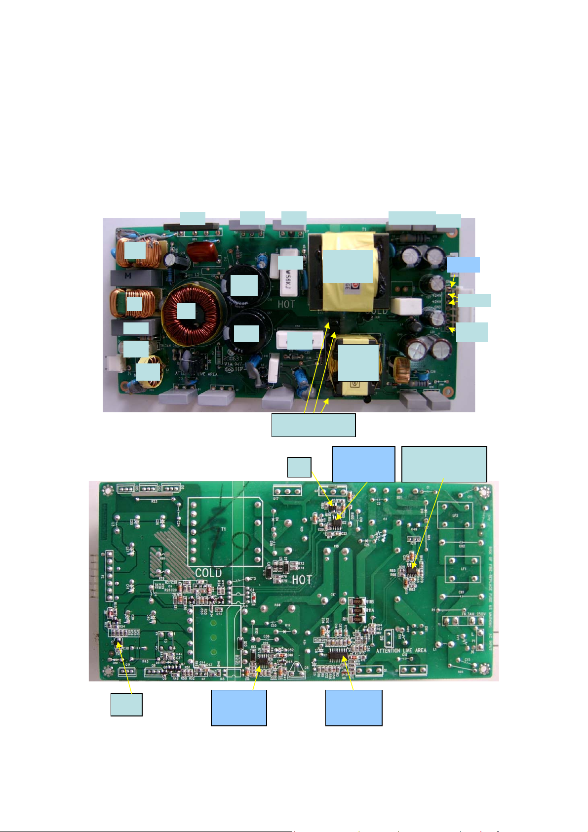
It has many protection functions such as OCP, OVP and over heat protection. Fig. 1-1
BD1
Q2
Q17
D8 Q13
Q15
P1
~220V
Input
LF2
CX1
LF1
F1
X2
L1
C49
D1
IC11
L2
C3
D9
Q1
C16
C17
R39
Q5
R16
R38
T1
+24V Output
IC3
IC5
T2
+12V
C26 C25
R79
C40
T3
Q6 Q14
C27
C41
C39
P_ON
+24V
+24V
+12V
IC8 Photo Coupler
Q2
IC2 NCP1217
PWM
IC10 LM393
Low Power Low Offset
Q11
IC6 NCP1377
PWM Curre nt
IC1 NCP1650
Power Factor
Fig. 1-1 PWL371 1C
2
Page 3

The switch power supply has two operation conditions:
1) Normal-Normal work when power on;
2) Standby-When TV set standby, switch power supply is in narrow pulse operation condition and
change to under voltage condition, then the output voltage goes down to half value of normal
condition;
The theory introduction of each part of the switch power supply as following:
I Anti-interference circuit
When switch on, the commercial AC220V/50Hz passes common-mode filter composed of fuse F1、
ZV1、R1、CX1、CX2、LF1|、LF2 to eliminate the all the EMI and high frequency interference pulse from
power input port.
X capacity and Y capacity are both safety capacitance. The difference of them is that X capacitance is
connected to AC input port to eliminate difference-mode interference, Y capacitance is connected between
AC input and ground to eliminate common-mode interference. Y capacitance has two kinds, one is Y1
capacitance belonging to double insulation Y capacitance and connecting between primary coil and second
coil, the other is Y2 capacitance belonging to basic single insulation Y capacitance and connecting between
primary coil to protect ground.
II Commutating Filter Circuit
BD1、C1、C2 compose bridge commutating circuit to convert the 220 AC to 300 DC filtered by C3.
III PFC Circuit
PFC circuit is composed of IC1(NCP1650),Q1,L2 and the other external components.
NCP1650 Power Factor Controller Introduction
NCP1650 chip is an active, power factor correction controller that can operate over a wide range of
input voltages, and output power level. It is designed to operate on 50/60Hz power system. This controller
offers severl different protection methods to assure safe, reliable operation under any conditions.
1、Feature:
Fixed Frequency Operation
Average Current Mode PWM
Continuous or Discontinuous Mode
Operation
Fast Line/Load Transient Compensation
True Power Limiting Circuit
High Accuracy Multipliers
2、Block Diagram
Undervoltage Lockout
Overvoltage Limiting Comparator
Brown Out Protection
Ramp Compensation Does Not Affect
Oscillator Accuracy
Operation from 25 to 250kHz
3
Page 4
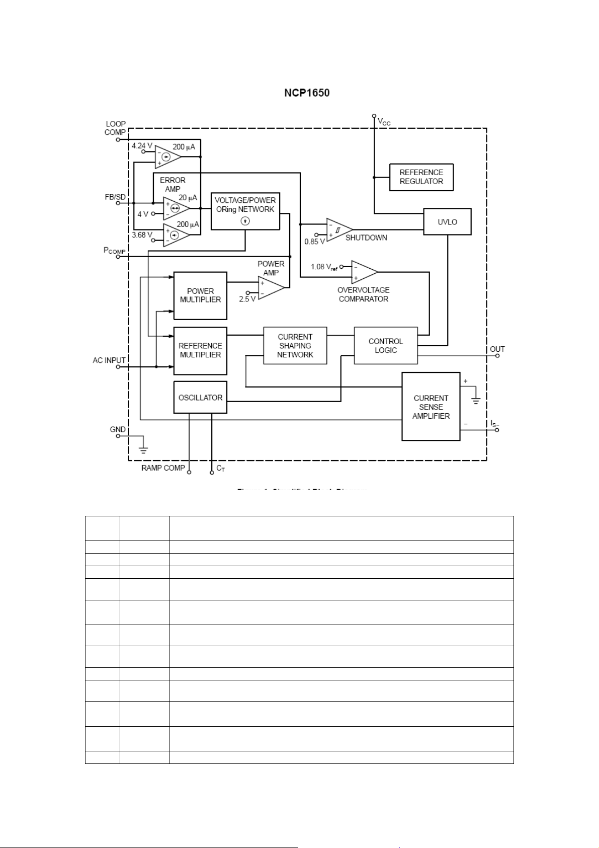
Fig.1-2 NCP1650 inner block diagram
3、Pin Function Description
Pin
Function Function
No.
1 Vcc
2 V ref
3 Acc
4 AC ref
5 AC
Provides power to the device
6.5volt regulated reference output.
Provides pole for the AC Reference Amplifier
This pin accommodates a capacitor to ground for filtering and stability of the ac error
amplifier
The rectified input ac rectified sinewave is connected to pin.
input
6 FB
7 Loop
8 Pcom
9 Pmax
The DC output of the converter is reduced throug resistive divider, to a level of 4.0 volts,
and connected to this pin to provide feedback for the voltage regulation loop.
A compensation network for the voltage regulation loop,is connected to the output of the
power error amplifier at this pin.
A compensation network for the maximum power loop
This pin allows the output of the power multiplier to be scaled for the desired maximum
power limit level
10 Iavg An external resistor with a low temperature coefficient connected from this
terminal to ground
11 Iavgfltr A capacitor connected to this pin filters the high frequency component from
the instantaneous current wave
12 Is- Negative current sense input.
4
Page 5
13 Ramp c This pin biases the ramp compensation circuit
14 CT Timing capacitor for the internal oscillator.
15 GND Grount reference for the circuit
16 DRV Drive output for power FET or IGBT.
4、NCP1650 test parameter:
Pin no Red probe connect
GND
Voltage Pin no Red probe connect
GND
Voltage
1 20K 12V 9 30K 0
2 15K 6.5V 10 13K 0
3 5K 0 11 5K 0
4 5K 0 12 0 0
5 17K 2V 13 42K 2V
6 28K 4V 14 4K 2V
7 6K 4.5V 15 0 0
8 5K 0 16
3 欧
0
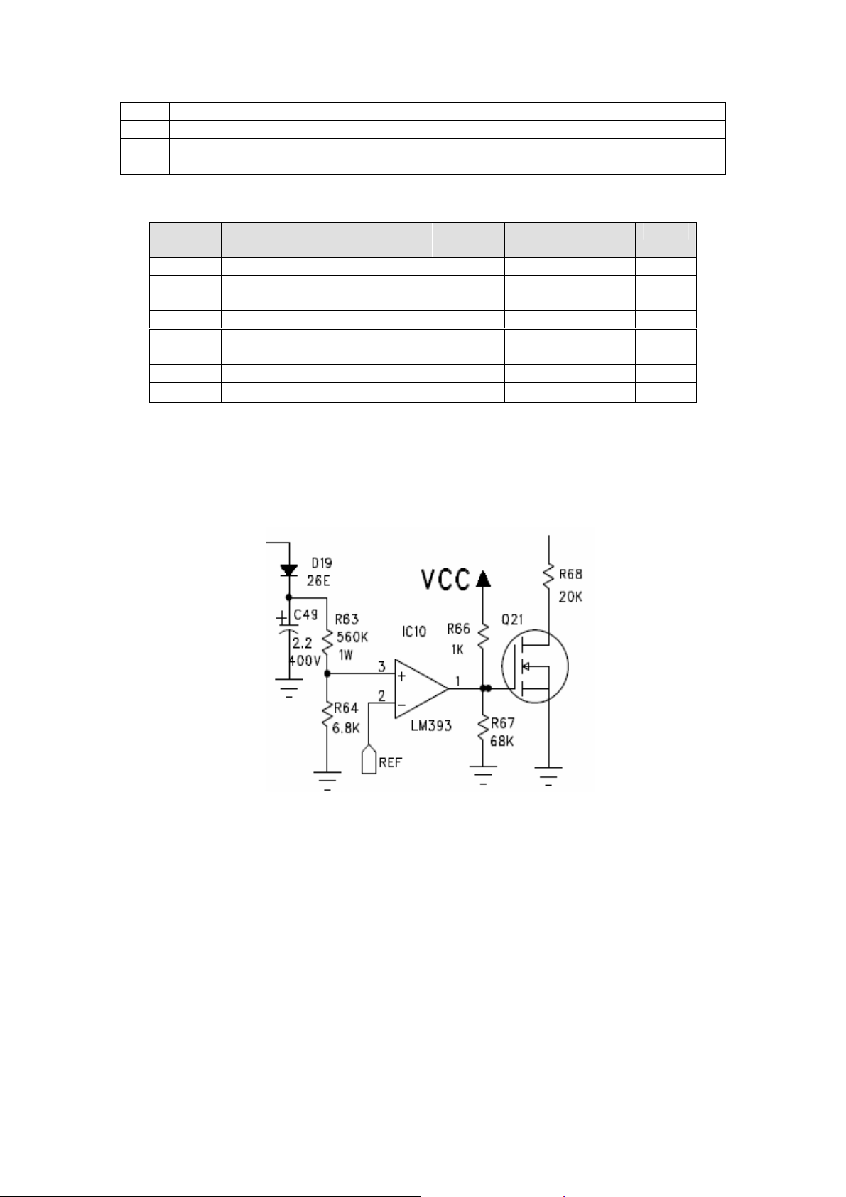
PFC circuit of PWL3711C is fixed frequency average current mode boost converter. PFC circuit
operates in two stages: 90Vac ~132Vac is the low input stage for PFC output 260VDC;180Vac~
264Vac is high input stage for PFC output 390VDC. The shift stage is 140Vac~165Vac
completed by comparator IC10. When input commercial current in high stage, the level of pin 3 of
IC10 is higher than pin2, then Q21 turns on to make sample voltage of IC1 FB(pin6) go down and
make the output voltage of PFC go up to 390VDC.
Fig.1-3 High and low voltage shift circuit
The operation frequency is about 70KHz.The output current changing should follow input
voltage changing to go to pin5/pin12 of IC and the voltage entering pin6 of IC. When the inner
parameters are compared and calculated to confirm the operation duty ratio and maintain the
stabile voltage. Under the stable output power, the input voltage decrease, minimum duty ratio of
the output pulse width of IC1 largen. When input voltage increases, the minimum duty ratio of
pulse width output will decrease; vice versa.
In an output cycle, duty ratio of IC1 pulse width output is mutative in which there is a
minimum duty ratio on the highest point of Vac. As shown fig. 1-4:
5
Page 6

V1I Vac
Q1 alternating with D1 produce output current of bridge commutating diode to flow
continuously, and the angle of flow go to 180°so that the current of AC has the same phase with
voltage of AC . The waveform is sine wave, and the power factor of system should approach to 1.
Switch: ON or OFF
IL
Iac
t 0
Fig. 1-4
IV DC-DC Shift:
1、12V Section
(1)、IC6-NCP1377
NCP1377 PWM Current-Mode Power Supply Controller
NCP1377 combines a true current mode modulator and a demagnetization detector which
ensures full borderline/critical Conduction Mode in any load/line conditions together with
minimum drain voltage switching. Due to its inherent skip cycle capability, the controller enters
burst mode as soon as the power demand falls below a predetermined level. As this happens at low
peak current, no audible noise can be heard.
The transformer core reset detection is done through an auxiliary winding which, brought via
a dedicated pin, also enables fast Over Voltage Protection. Once an OVP has been detected, the IC
permanently latches-off. The 1377 features a sampling time of 4.5us whereas it is 1.5us for the B
version.
The NCP1377 also features an efficient protective circuitries which, in presence of an
overcurrent condition, disables the output pulse and enters a safe burst mode, trying to restart.
Once the default has gone, the device auto-recovers. Finally an internal 1.0 ms soft-start
eliminates the traditional startup stress.
(2)、 Features
Free-running borderline/critical mode
quasi-resonant operation
Lockout OVP
Auto-recovery short-circuit protection via
UVLO crossover
External latch triggering, e.g. via
overtemperature signal
Current-mode with adjustable skip-cycle
capability
Internal 1.0 ms soft-start
Internal temperature shutdown
Internal leading edge blanking
500mA peak current source/sink
capability
Under voltage lockout level of 12.5V
(On)and 7.5V(Min)
Direct optocoupler connection
6
Page 7
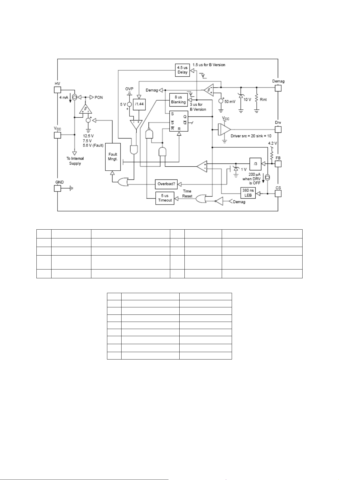
(3)、Internal Block
Fig.1-5 NCP1377 Internal Circuit Architecture
(4)、Pin Function Description
Pin Symbol Function Pin Symbol Function
1 Demag Core reset detection and OVP 5 Drv Driving pulse
2 FB Sets the peak current setpoint 6 Vcc Supplies the IC
3 CS Current sense input and skip
7 NC
cycle level selection
4 Gnd The IC ground 8 HV High-voltage pin
(5)、NCP 1377 test parameters:
Pin Red probe to ground Voltage
1 13K 0
2 41K 0
3 1K 0
4 0 0
5 3K 0
6
30Ω
7
∞
10V
0
8 400K 350V
Pin8 of IC6 connects R101 to “+”end of C16 via internal 4mA constant-current source to
charge C34. When reaches about 12.5V, output of pin5 of IC6 is pulse width waveform and 4mA
constant-current sourse will shut off, then auxiliary winding of transformer T2 supplies C34.
Because of PFC circuit, voltage of C16 is constant, and the changing of duty ratio of IC6 is
only with output load. At the moment of output loads enhance, 12V drops and the current of IC8
reduces, then level of pin12 of IC6 goes up, so largens pulse width duty ratio of IC6 and makes
the turn-on time longer to make transformer transmit more energy. Output of 12V goes up to
largen turn-on current of IC8. Shown as fig. 1-6.
7
Page 8
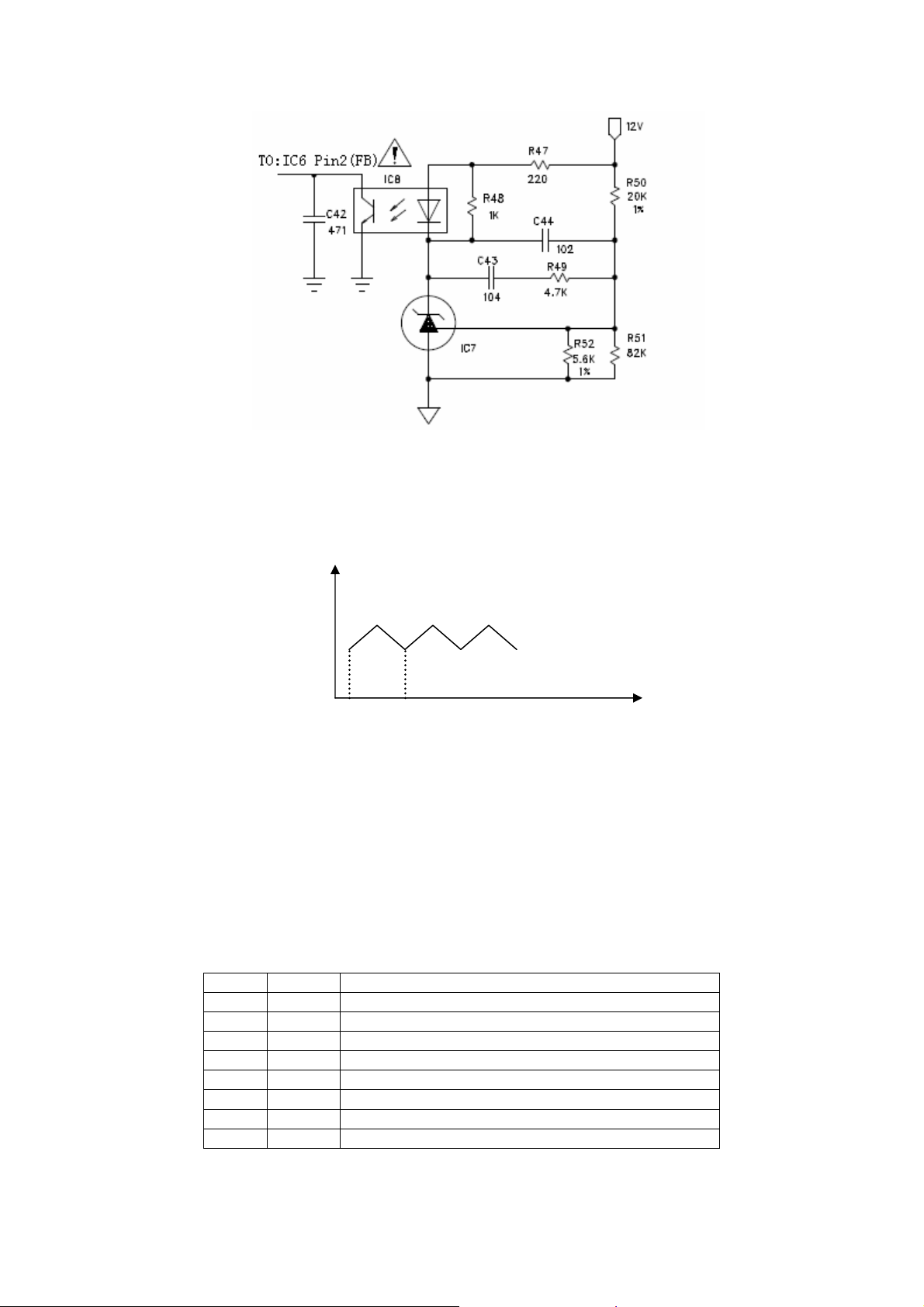
Fig. 1-6 12V branch feedback circuit
In fact, under output load changeless, IC6 also performs the above adjustment, but the adjustment
amplitude is slight. Output constant voltage relies to above closed loop adjustment, so that forms
output voltage ripple form:Fig. 1-9
V
12V
10us
One operation cycle
t 0
Fig. 1-9
2、24V Section
24V branch section is basic sameness to 12V section, but only little difference in function of IC
NCP1217(IC2) is current mode PWM controller, applying to offline switch power supply.
(1)Feature
1、 Current-mode with adjustable skip-cycle capability
2、 Built-in internal ramp compensation
3、 Auto-recovery internal output short-circuit protection
4、 Internal 1.0ms soft-start
5、 Fixed frequency versions at 65kHz, 100kHz and 133kHz
(2)Pin function description
Pin No Symbol Function
1 Adj Adjust the skipping peak current
2 FB Sets the peak current setpoint
3 CS Current sense input
4 Gnd IC Ground
5 Drv Drive pulse
6 VCC supplies the IC
7 NC
8 HV Ensures a clean and lossless startup sequence
(3)Internal Circuit architecture
8
Page 9
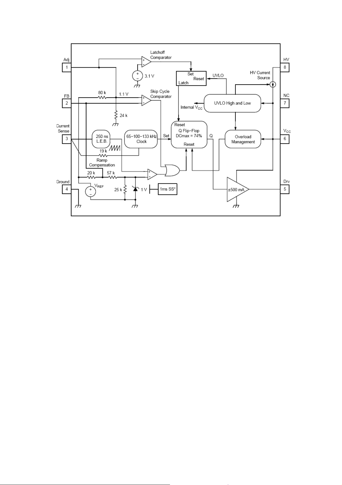
Fig. 1-10 NCP1217 Internal Circuit architecture
V Switch Voltage Regulated Circuit
1、Power Supply DC Output
24V/4A power supply branch: One way goes directly to primary winding passing primary
winding 1-3 to pin D of Q2/ Q17; the other way passing D3 and goes directly to pin8 of IC2
connecting internal circuit of IC to pin6 to charge C21. When the voltage setpoint reaches 12.5V,
IC2 operates normally and internal circuit latches off between pin6 and pin8, then C21 discharges
through internal circuit of IC2. At the same time, output of pin5 is driving signal to Q2/Q17 which
turns on, so the primary winding of T1 turns on to store the energy.
When C21 discharge to 5.6V, the discharge circuit shuts off and driving signal of pin5 latches
off , so each secondary winding of T1 induces output voltage via to energy shift.
At the same time, secondary winding pin6 charges C21 through L5/D7, when reaching 12.5V,
pin5 of IC2 sends out drive signal to Q2 and Q17 which turns on, so primary winding of T1 turns
on to enter new save energy loop process and ensure inducing constant output voltage from each
secondary winding.
When output of secondary reaches over 24V, the current of photocoupler IC3 enhances as
R24 sample voltage largens, so that photo coupler shines strongl y to feedback to pin2 of IC2, the
point voltage of this pin going low. Output signal of pin5 of IC2 shuts off to adjust duty ratio.
12V/4A power supply branch: One way to primary winding 1-3 of T2, then to D pin of Q5;
the other way via D11 to pin8 of IC6(NCP1377), connecting internal circuit of IC6 to charge C34,
9
Page 10

when voltage of C34 reaches 12.5V, IC6 starts up to operation, and the internal circuit disconnects
from pin6 and pin8. C21 discharges via internal circuit of IC6, and pin5 exports drive signal to
make Q5 turns on, so connects primary winding of T2, and T2 starts saving energy.
When C21 discharges to 5.6V, the discharge circuit will shut off, and output drive signal will
stop from pin5. For energy shift, inducing output voltage produces from each secondary winding
of T2.
At the meantime, secondary winding pin6 charges C34 via D13/R37, when the voltage
reaches 12.5V to drive pin5 to export drive signal, Q5 turns on and connects primary winding of
T2, then renews to save energy to ensure constant inducing output voltage from each secondary
winding.
When output voltage of secondary winding reaches 12V, the current of passing photocoupler
IC8 enhance, so the photocoupler shines strongly to feedback to pin2 of IC6, the level of this pin
goes down to output signal of pin5 of IC6 shuts off to adjust duty ratio to ensure constant output
voltage 12V.
2、Over-Current Protection
24V/4A supply power branch
The sample current passes R20 to get the sample voltage which on R17 to connect internal
circuit of pin3 of IC2. When the sample current reaches a certain rated value, IC2 stops to work
and protects the circuit.
12V/4A supply power branch
The sample current passes R39 to get sample voltage which is on R42 to connect internal
circuit of IC6’s pin3. When the sample current reaches a certain rated value, IC6 would stop to
work to protect the circuit.
3、OVP Circuit
12V/4A Supply Power Branch
Secondary winding pin5 of T2 connects IC6’s pin1 via R35, when testing circuit of IC6 test
the voltage over the rated value, IC6’s pin5 stops to export drive signal to make Q5 shut off.
When canceling the test signal, IC6’s pin5 exports drive signal again to make Q5 turn on and
continue to operate
24V/6A Supply Power Branch
when the output is higher than 31V, so ZD2 and ZD3 work normally and signal 24V-OVP
is high level. Q3’s pinC connects to ground. The current between pin1and pin2 of IC3, so inner
diode shines strongly, the current largen between pin3 and pin4. This signal is sent to pin2 of IC2
to latch off the drive signal. The power is off.When the high level signal 24V-OVP is sent to pinB
of Q12, Q12 turns on to the ground. The photo coupler is shines strongly and the current of
receiver increases. So the low level is sent to pin8 of IC2 to shut off the power.
10
Page 11

4、Power Standby
When plug in AC commercial current, the 12V of power supply continues to operate, power
supply standby circuit control is only for 24V supply.
Remote control signal connect P2’s pin1 via J2’s pin4 to passing R33 to B pin of Q4. When
receives power on signal, the B pin of Q4 is low level, Q4 turns on and Q12 shuts off.
Standby circuit
Fig. 1-11 Standby control circuit
Power off: when receives the remote signal low, Q4 shuts off and Q12 turns on. Because of
induction action of photocoupler, the level of IC2’s pin2 is pulled low, so IC2 stops to operate
Power on: when receives power on high level signal, Q4 turns on and B pin of Q12 equals to
connect ground. For photocoupler doesn’t work, IC2’s pin2 releases and this setpoint voltage is
high level. IC2 renews to operate to export drive signal from pin5, so the circuit exports 24V
power supply.
VI 、LCD3711C Power Supply Block Diagram.
11
Page 12

~220VAC
P_ON
Filter(LF1,
LF2,
CX1,CX2,
CY1,CY2)
High and Low
Voltage Converter
Circuit(IC10,Q21)
Standby and
Power on Circuit
(Q4,IC5)
Commutation
Circuit(BD1,C
3)
Transformer
T1
PFC
Circuit
( IC1,Q
Q2 Switch
PWM
Transistor
Circuit (IC2
Q2,Q17)
OCP Circuit (R20,R17)
Transformer
T2
Rectifier L3,D8,
Q13,Q15,C25)
+24V/6
OVP and
Stabilized
Voltage Circuit
( IC3,IC4,
Q3,ZD2, ZD3)
PWM
Circuit
(IC6)
Q5 Switch
Transistor
OCP Circuit
(R39,R42)
12
Synchronous
+12V/4
Rectifier
(T3,Q7,Q6)
Stabilized Voltage
Circuit (IC8,IC7)
Page 13

VII Trouble Shooting
e.g1 No Power
No Power
F1 burned
HV is lower
than 130V
HV ok,
No +12V
+12V OK,
No +24V
Mark: There are two supply outputs: +12V and + 24V by different transformer in this power
supply solution. When TV switch on, +12V output is ok to all the boards; then send standby
signal to power on, +24V output to the panel.
If HV is higher than130V, but High and Low Voltage Converter Circuit don’t work,
+12V and +24V output will be still ok.
13
Page 14

e.g2 No +12V, No +24V trouble shootin
g
F1 burned
Test if pin
pinS of Q1,
Q2,Q17,Q5
to ground?
N
Replace
C3,C16,C17,
C49, F1 ok?
N
Problem
from others
boards or
panel
OVER
Test and
Replace the
bad
14
Page 15

g
e.g2 No +12V, No +24V trouble shootin
HV is lower
than 130V
Test if pin
pinS of Q1,
Q2,Q17,Q5
to ground?
N
Is the impidance of IC2’s pin8,
IC6’s pin8, IC1’s pin5 low
N
Is BD1 OK?
Y
Replace R1
OVER
Y
Test and
Replace
the bad
Y
Test and
Replace
the bad
15
Page 16

e.g2 No +12V, No +24V trouble shooting
HV ok , no
+12V
+12V Repair
Stabilized
circuit
Y
IsIC’s pin8
N
over 130V
Y
Is IC’s pin5
N
about 10V?
Y
Test
Q14,Q6-Q9
N
OK?
Y
Voltage of IC6’s pin2 change from
3.8V to 4.2 again and again
N
Replace
IC6
Replace
IC 6 or
R101
Replace
IC 6 or
C34,ZD5
Replace
IC 6 or
C34,ZD5
OVER
16
Page 17

e.g3. +12V OK, No +24V trouble shootin
g
+12V OK, No +24V
Is 24V-OVP 0.7V?
N
P_ON is over 2V, is
pinC of Q12 12V?
Y
Is the voltage of
IC2’s pin8 over
130V?
Y
N
N
Test ZD2,ZD3 and
replace the bad.
Test IC5,Q12,
Q4,Q16and ambient
parts, replace the bad
Test IC2,R100 and
replace the bad
Y
Is the voltage of
IC2’s pin6 12V?
Y
Is PWM waveform
of IC2’pin5 is ok?
N
Is the voltage of
IC2’pin2 about 8V ?
N
Replace IC2
OVER
Test IC2,C21,ZD1
N
and replace the
bad
Y
Test Q20,Q2,Q17
and replace the bad
Y
Repair the stabilized
circuit
17
Page 18

VIII Repairing
1、A 40W bulb is necessary to be connected between the AC lines and lest the power board damaged.
The bulk will twinkle if the PWB is good. The input power is about several decades Watt. You can
measure 12V and 24V can be measured when P-ON voltage is given or connected with 12V;If the bulb
is lightening and no output is detected, the PWB still need further repairing.
2、Possible defective cause: ①defective Design ②defective Ma terial ③Producing engineering problem:
short circuit(soldering-connected, pin-shorted),open-circuit(false soldering, pin-unconnected)
3、Troubleshooting steps: ①If the fuse is OK and no output, IC is possibly damaged or shut down
under protective status. The other side, if the fuse is broken, you should check more parts like IC,
MOSFET, Diodes, Zener diode etc. ②You should know the pin functions of IC
Checking IC2 and IC6, 13V DC supply to VCC with no AC input. Test the voltage of PIN2 if the
voltage is 4.2VDC or not, and test if the output pulse width decrease or not by an oscilloscope. If not,
replace the IC.
4、Holes of double-face board , small copper wire will easy open when the power board pass oven ,it’s
not easy to be found, the places where is easy open are MOSFET S pole to grounding, drive circuit
and ISENCE circuit.
5、Component check: transformer /inductance /photo coupler /TL431 on the power board aren’t easy to
damage , most MOSFET damage is like G-S short circuit ,G-D-S short circuit, even crack, most
transistors damage are as B-E short circuit, C-B-E short circuit even crack., diode damage is as
short circuit. Zener diode damage is open circuit even crack. IC2 damage is possible ground to
output(D1) short circuit or less than 0.5; ground to VCC(D1)short circuit or less than 0.5 even crack.
Resistor damage is the resistance value increase even crack. SMD Capacitor damage is crack or
capability too large ; electrolytic capacitance damage is crack, plump , electrolyte leakage .
18
Page 19

PWL3711C-SMPS.schH.sch-1 - Mon Nov 06 10:19:07 2006
Page 20

Chapter II PWL3708B-SMPS and PWL3711C
The theory of these two switch power supply can refer to the description of LCD3711c.
Chapter III ON37A switch power supply
I About ON37A Power Supply
ON37A power supply circuit was designed by TCL R&D center, The circuit adopt PFC control IC
NCP1653 and PWM control IC NCP1377,it has over voltage protection, over current protection ,over hot
protection function etc. IC’s Follow Boost pattern can increase whole circuit efficiency at low voltage ,
increase dependable stability, and it can eliminate noise on some point of load, it make the unit’s
performance more steady. (Please refer to ON37A Schematic Diagram)
20
Page 21

U5 IC NCP1377
PWM Controller
U7 IC LM393
Dual Comparator
U6 IC NCP1655
PFC Controller
21
Page 22

II Circuit Diagram
Fig4-1 ON37A Power Supply Block Diagram
AC IN
EMC
Filter wave
circuit
Bridge
commutate
PFC control
circuit
Control IC
NCP1653
VCC control cell
Standby circuit
Control IC
VIPer22ADIP
PWM control
circuit
Control IC
NCP1377
Isolation
transforme
r
PS-ON
Isolation
transformer
Output voltage
commutate
filter wave
Over current, over
voltage protection,
standby control circuit
output
voltage
commutate
Photocoupler
insolation control
Main power
+24V/+12V/+18V
Standby
voltage
22
Page 23

III Operation Theory
1、Input Circuit
When turns on the power switch, AC220V/50Hz passes common model filter consisted of
fuse F801、RV801、C819、L806、LF802、LF801、R824 etc, it will restrain multiplicate
electromagnetism interference from power supply circuit and eliminate high frequency interfere
pulse from electricity net voltage .after BD1 bridge commutate , about 300V direct current output.
DC 300V is processed by each control circuit.
2、Standby Start-up Circuit
After being commutated to output 300v voltage ,one way is through D819.R832 connecting
with transformer T803’s primary coil , pin3 connect with pin5/Pin6/Pin7/Pin8 of IC U4,through
U4 inner start circuit connect with pin4 VDD of U4, cause U4 ‘s Source-Drain switch on, so that it
makes the T803’s primary coil work , so secondary coil output inductive 5V standby voltage.
DC 300V after
commutating
Transformer T803’s secondary winding pin4 is separated
2 ways , one way output 15V VCC voltage ,supply power to
IC , the other way through diode connect with pin4 of U4 to
supply power for U4.
After commutating, output voltage of the secondary
winding’s pin6 is sampled via R838, The sampling voltage input pin1 of U3, and the current occur
between the pin3 and pin4 of photo coupler U3.The change of the current input pin4 and pin3 of
U4, and the U4 adjust PWM to control transformer to output steady 5v standby voltage.
Fig 4-2 Standby Start-up Circuit 1
23
Page 24

Fig 4-2 Standby Start-up Circuit 2
3、Standby Control Circuit
While connecting AC power supply, the standby circuit wait to start.
Others control circuit units can startup After the standby circuit work under normal
situation .Then the main transformer start working, and output power supply 24V and 12V.
①Power On
When the control unit send one high level signal via pin3 of P802 to pin B of Q808 through
R842、R841、D819, Q808 turn on , In the meantime, pin1 and pin2 of photo coupler U2 is on, so
inductive current pass pin3 and pin4 of U2. It makes pole B of Q807 has low level and turn on.
The 15V supply power VCC1 and VCC2 to pin6 of U5 and pin8 of U6.
②Standby
Fig4-3 Standby、Turn on control Circuitry
24
Page 25

The otherwise, when pin3 of P802 send a control signal which is low level. The signal passes
R842.R841.D819 to pole B of Q808 and Q808 shut down, then pin1 and pin2 of photo coupler U2
open, therefore it doesn’t wok, pin4 and pin3 of U2 open too, then Q807 shut down, 15V VCC
power supply voltage can’t supply VCC2 and VCC1, and U5 and U6 can’t get the working
voltage, so U5,U6 stop working.
4、 PFC Circuit
While VCC1 is about 15v voltage to supply pin8 of U6 (NCP1653A), U6 start working, and
pin7 of U6 output pulse signal to pole B of Q801.
Fig 4-4 NCP1653A scheme diagram
The pulse signal control Q801 turning on an d shutting down, so it makes L801 repeat save
energy and discharge power, After being commutated, the voltage increase to about 390v, filtered
by C807 send to PWM circuit.
25
Page 26

Fig4-5 PFC switch control circuitry
PFC circuit adjustment is finished by pin1/pin3/pin4of U6 .
Bridge rectifier output voltage through resistance R860.R1.R864.R865.R867 and connect
with pin3 of U6,for input voltage limit controlling.
PFC circuit output voltage passes R862、R861、R863、R866 to connect with pin1 of U6.As
feedback signal , inner circuit of U6 adjust and control pulse width signal output from pin7.In
addition, it is over voltage protection function .
The negative current of PFC circuit passes R869 to connect pin4 of U6.
5、PWM Circuit
When VCC2 is about 15v voltage and connect with pin6 of U5,U5 start working to make
pin5 of U5 export pulse control signal to pole B of Q805 and Q802.
26
Page 27

Figure 4-6 NCP1377circuit diagram
When the pulse signal is high level,Q805 cut off and Q802 turn on. VCC2 passes Q802/R813
to charge up C820. when the pulse signal is low level, Q802 cut off and Q805 turn on. C820
discharge from Q805. As C820 repeats charging and discharging , that make pin1 and pin2 of
transformer T802 primary coil discharging or charging, so there is the inductive current in pin6
&pin5 and pin4 & pin3of secondary coil. The drive signal control Q803 and Q806 to close and
open.
For Q803 and Q806 close and open to make output voltage of PFC circuit which connect
with primary coil of the transformer to repeat saving energy and release energy. So the inductive
output voltage of secondary coil export 24V and 12V to main board.
Fig4-7 PWM control circuit diagram
6、Regulated Voltage Circuit
Regulated voltage Circuit is controlled by U5 and export 24V through R803 connecting with
pin1 and pin2 of U1.
Because of photo coupler , inductive current occur between pin3 and pin4 of U1, and pin4
of U1 connects with pin2 of U5. The feedback signal will be sent to inner of U5 to adjust the
pulse output from pin5 of U5 which keep transformer T801 output steady voltage.
27
Page 28

7、Over Voltage Protecti on
Output circuit of +24V and +12V connect with rectifier diode D804 and D806, then
incorporate the them into one way then pass D809/R856 to connect with pole B of Q812.
While work normally, pole B of Q812 is low level, then Q812 and Q810 cut off.
When main voltage 24V and 12V is over voltage , pole B of Q812 is high level, then pole B
of Q810 is high level, so that Q812 turn on to makes Q810 turn on, through diode D820
connecting with resistance R842 to pull the voltage down. That makes the power on high level
signal not work, which equal to turn off signal. So the power shuts down. and stops working.
8、Over Current Protection Circuit
In 12V output circuit, pin13 of secondary winding of transformer connects with R908 and
R902 to pin2 of U7 A.
Fig.4-8 Over current protection circuit
While over current occur, pin1 of U7A exports negative voltage and pin7 of U7B exports negative
voltage too. The negative voltage connects with the pole B of Q801 to make the Q810 turn on,
then passes D820 and connect with R842. That makes the voltage of this point go down quickly.
So high level of turning on signal doesn’t work equaling to turning off signal. The power shuts
down and stop working.
28
Page 29

MON37A-PW.sch-1 - Thu Nov 02 11:05:28 2006
 Loading...