

Page 1

TCL
Service Manual
CHASSIS MT62LV
Content s
1. Caution .…………………...................................................................…………...………..2
2. Test and Alignment………………….………………………………...………..7
3. Block Diagram………………………………….…….. .......................……..25
4. MB Schematic Diagram……………… …………….......................……….26
5. PSU Schematic Diagram..........................................................................43
6. Exploded View
....................................
................
.................................
44
Page 2
CAUTION:
1、
Use of controls, adjustments or procedures other than those specified herein may result in
hazardous radiation exposure.
CAUTION: TO REDUCE THE RISK OF
CAUTION
RISK RISK OF OF ELECTRIELECTRICC
SHOCK SHOCK DO DO NOT NOT OPEN.OPEN.
The lighting flash with arrowhead symbol, with an equilateral triangle is intended to
alert the user to the presence of uninsulated voltage within the product s
enclosure that may be of sufficient magnitude to constitute a risk of electric shock to
the person.
The exclamation point within an equilateral triangle is intended to alert the user to the
presence of important operating and maintenance (servicing) instructions in the
literature accompanying the appliance.
ELECTRICAL SHOCK, DO NOT REMOVE
COVER (OR BACK). NO USER SERVICEABLE
PARTS INSIDE. REFER SERVICING TO
QUALIFIED SERVICE PERSONNEL.
dangerous
WARNING: TO REDUCE RISK OF FIRE OR ELECTRIC SHOCK, DO NOT
EXPOSE THIS APPLIANCE TO RAIN OR MOISTURE.
Page 3

IMPORTANT SAFETY INSTRUCTIONS
CAUTION:
Read all of these instructions. Save these instructions for later use . Follow all Warnings and
Instructions marked on the audio equipment.
1. Read Instructions- All the safety and operating instructions should be read before the product is operated.
2. Retain Instructions- The safety and operating instructions should be retained for future reference.
3. Heed Warnings- All warnings on the product and in the operating instructions should be adhered to.
4. Follow Instructions- All operating and use instructions should be followed.
FOR YOUR PERSONAL SAFETY
1. When the power cord or plug is damaged or frayed, unplug this television set from the wall outlet and refer servicing to
qualified service personnel.
2. Do not overload wall outlets and extension cords as this can result in fire or electric shock.
3. Do not allow anything to rest on or roll over the power cord, and do not place the TV where power cord is subject to
traffic or abuse. This may result in a shock or fire hazard.
4. Do not attempt to service this television set yourself as opening or removing covers may expose you to dangerous
voltage or other hazards. Refer all servicing to qualified service personnel.
5. Never push objects of any kind into this television set through cabinet slots as they may touch dangerous voltage
points or short out parts that could result in a fire or electric shock. Never spill liquid of any kind on the television set.
6. If the television set has been dropped or the cabinet has been damaged, unplug this television set from the wall outlet
and refer servicing to qualified service personnel.
7. If liquid has been spilled into the television set, unplug this television set from the wall outlet and refer servicing to
qualified service personnel.
8. Do not subject your television set to impact of any kind. Be particularly careful not to damage the picture tube surface.
9. Unplug this television set from the wall outlet before cleaning. Do not use liquid cleaners or aerosol cleaners. Use a
damp cloth for cleaning.
10.1. Do not place this television set on an unstable cart, stand, or table. The television set may fall, causing serious injury
to a child or an adult, and serious damage to the appliance . Use only with a car t or stand recommended by the
manufacturer, or sold with the television set. Wall or shelf mounting should follow the manufacturer s instructions, and
should use a mounting kit approved by the manufacturer.
10.2. An appliance and car t combination should be moved with care. Quick stops, excessive force, and uneven surfaces
may cause the appliance and cart combination to overturn.
Page 4
PROTECTION AND LOCATION OF YOUR SET
11. Do not use this television set near water ... for example, near a bathtub, washbowl, kitchen sink, or laundry tub, in a
wet basement, or near a swimming pool, etc.
Never expose the set to rain or water. If the set has been exposed to rain or water, unplug the set from the wall
outlet and refer servicing to qualified service personnel.
12. Choose a place where light (artificial or sunlight) does not shine directly on the screen.
13. Avoid dusty places, since piling up of dust inside TV chassis may cause failure of the set when high humidity persists.
14. The set has slots, or openings in the cabinet for ventilation purposes, to provide reliable operation of the receiver, to
protect it from overheating. These openings must not be blocked or covered.
Never cover the slots or openings with cloth or other material.
Never block the bottom ventilation slots of the set by placing it on a bed, sofa, rug, etc.
Never place the set near or over a radiator or heat register.
Never place the set in enclosure, unless proper ventilation is provided.
a built-in
PROTECTION AND LOCATION OF YOUR SET
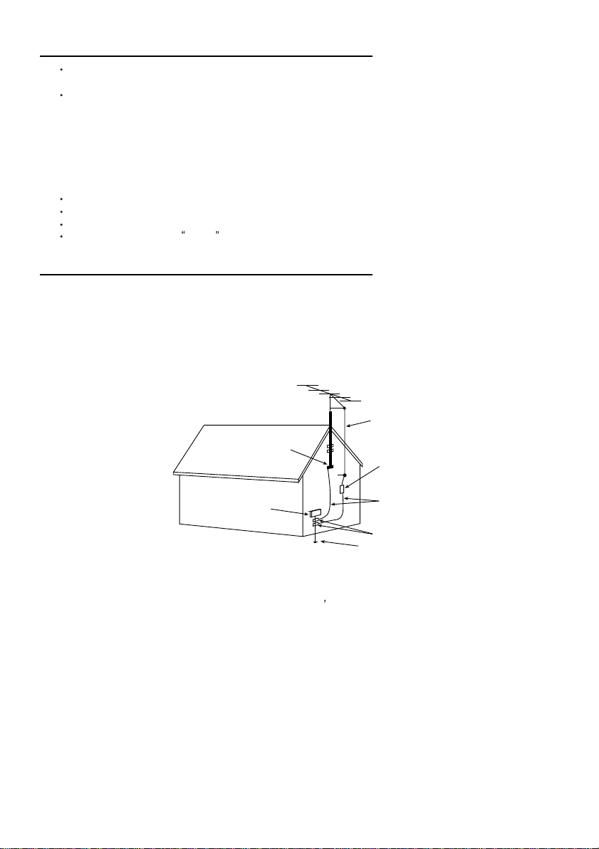
15.1. If an outside antenna is connected to the television set, be sure the antenna system is grounded so as to provide some
protection against voltage surges and built up static charges, Section 810 of the National Electrical Code, NFPA No.
70-1975, provides information with respect to proper grounding of the mast and supporting structure, grounding of the
lead-in wire to an antenna discharge unit, size of grounding conductors, location of antenna discharge unit, connection
to grounding electrode, and requirements for the grounding electrode.
EXAMPLE OF ANTENNA GROUNDING AS PER NATIONAL ELECTRICAL CODE INSTRUCTIONS
EXAMPLE OF ANTENNA GROUNDING AS PER
NATIONALELECTRICAL CODE
ANTENNA
LEAD- INWIRE
GROUND CLAMP
ELECTRIC SERVICE
EQUIPMENT
NEC-NATIONALELECTRICAL CODE
ANTENNA DISCHARGE
UNIT (NEC SECTION
810-20)
GROUNDING
CONDUCTORS
(NECSECTION 810-21)
GROUND CLAMPS
POWER SERVICE GROUNDING
ELECTRODE SYSTEM
(NEC ART 250. PARTH)
15.2. Note to CATV system installer : (Only for the television set with CATV reception)
This reminder is provided to call the CATV system attention to Article 820-40 of the NEC that provides
installer s
guidelines for proper grounding and, in part icular, specifies that the cable ground shall be connected to the grounding
system of the building, as close to the point of cable entry as practical.
16. An outside antenna system should not be located in the vicinity of overhead power lines or other electric lights or power
circuits, or where it can fall into such power lines or circuits. When installing an outside antenna system, extreme care
should be taken to keep from touching such power lines or circuits as contact with them might be fatal.
17. For added protection for this television set during a lightning storm, or when it is left unattended and unused for long
periods of time, unplug it from the wall outlet and disconnect the antenna. This will prevent damage due to lightning
and power-line surges.
Page 5

OPERATION OF YOUR SET
18.
This television set should be operated only from the type of power source indicated on the marking label. If you are not
sure of the type of power supply at your home, consult your television dealer or local power company. For television
sets designed to operate from battery power, refer to the operating instructions.
19. If the television set does not operate normally by following the operating instructions, unplug this television set from the
wall outlet and refer servicing to qualified service personnel. Adjust only those controls that are covered in the operating
instructions as improper adjustment of other controls may result in damage and will often require extensive work by a
qualified technician to restore the television set to normal operation.
20. When going on a holiday : If your television set is to remain unused for a period of time, for instance, when you go on
a holiday, turn the television set and unplug the television set from the wall outlet.
off
IF THE SET DOES NOT OPERATE PROPERLY
21. If you are unable to restore normal operation by following the detailed procedure in your operating instructions,
do not attempt any further adjustment. Unplug the set and call your dealer or service technician.
22. Whenever the television set is damaged or fails, or a distinct change in performance indicates a need for
service, unplug the set and have it checked by a professional service technician.
23. It is normal for some TV sets to make occasional snapping or popping sounds, particularly when being
turned on or off. If the snapping or popping is continuous or frequent, unplug the set and consult your
dealer or service technician.
FOR SERVICE AND MODIFICATION
24. Do not use attachments not recommended by the television set manufacturer as they may cause hazards.
25. When replacement parts are required, be sure the service technician has used replacement parts specified
by the manufacturer that have the same characteristics as the original part. Unauthorized substitutions
may result in fire, electric shock, or other hazards.
26. Upon completion of any service or repairs to the television set, ask the service technician to perform
routine safety checks to determine that the television is in safe operating condition.
Page 6

Factory Alignment Specification of normal SIACP
TCL WW R&D
FPD CENTER
Factory Alignment Specification of normal SIACP
For MT5362 serial
Version:V0.51
For the following Chassis:
MT62L:A mini edition of MT62B
MT62S: MT62B + MS6M20(MEMC module) for super slim LCD
MT62F:A full function edition of MT62B
MT62S2: MT62S + DVB-S/S2 for super slim LCD
MT62LV:MT62L + VGA source + headphone output
PREPARED BY : Lance Deng
APPROVED BY : DATE :
DATE : 2011-01-18
Page 7
Factory Alignment Specification of normal SIACP
Disclosure
The information contained in this document is proprietary to TCL SZ FPD lab and shall not be
disclosed by the recipient to third persons without the written permission of the team leader or
GM of R&D.
Revision History
Status, Ver Date, Drafter Description of changes
V0.10 2010-02-07 This is the first version of normal SIACP
·HDMI as the main absolute input
·The password of factory menu is 9735
V0.20 2010-04-14 ·Upgrade specs for High Pot. and Insulating Resist ance Tests
·Upgrade USB upgrade SW met ho d
V0.30 2010-06-09 ·Add RCU(remote control unit) selection for the models IP
before May of 2010 in factory menu:( “feature” sub page in
MT62L, “Project info” sub page in MT62F and MT62S)
RC199:RC1994***
RC200:RC3000***
V0.42 2010-10-15 Add MT62S2 Chassis,
V0.50 2010-10-26 Add MT62LV Chassis,
V0.51 2010-12-22 Add the statement that the adapter should meet the High Pot.
and Insulating Resistance requirement.
Page 8
Factory Alignment Specification of normal SIACP
These chassises are designed for European LCD TV with MPEG4. The main chip is from
Mediatec (MT5362 series) and supports below inputs and outputs:
class item MT62L MT62S MT62F MT62S2 MT62LV
ATV
( PAL B/G D/K I, SECAM
B/G D/K L/L)
DTV
(DVB-T,DVB-C,DVB-S/S2)
HDMI
(480i/p, 576i/p, 720p up to
1080i/p, compliant v1.2.
with HDCP)
VGA
VGA/DVI audio
CMP
(YPrPb can support from
input
&
output
function
Others
Serial connector of MT5362 definition:
Pin1:VCC Pin2:RXD Pin3:TXD Pin4:GND (MT62LV: Pin1:RXD Pin2:TXD Pin3:GND)
I2C connector of MEMC definition:
Pin1:VCC Pin2:GND Pin3:SCL Pin4:SDA
480i up to 1080p,audio)
SCART1
(CVBS & RGB,audio)
SCART2
(CVBS & YC,audio)
Side AV or back AV
(CVBS,audio)
USB player
(picture,video,audio)
SCART1 output
(CVBS,audio)
SCART2 output
(CVBS,audio)
Headphone output
SPDIF output
MEMC
CI+
Serial connector
I2C connector of MEMC
module
√ √ √ √ √
DVB-T DVB-T
DVB-C
2 5 3 5 2
√ √ √ √
√
√ √ √ √ √
√ √ √ √ √
Picture
(up to
SW)
√ √ √ √ √
√ √ √
Coaxial Optical Coaxial Optical Coaxial
√ √
√ √ √
P5 P16 P3 P16 P5
PM3 PM3
Share
with CMP
Picture,
Video,
audio
DVB-T
DVB-C
√
Back
AV
Picture,
Video,
audio
DVB-T
DVB-C
DVB-S/S2
Share
with CMP
Picture,
Video,
audio
DVB-T
√
Picture
(up to
SW)
Page 9

Factory Alignment Specification of normal SIACP
INFO:
ª All tests and measurements mentioned hereafter have to be carried out at a normal mains voltage
(220 ~ 240 VAC)
ª All voltages have to be measured with respect to ground, unless otherwise stated
ª All final tests have to be done on a complete set including LCD panel in a room with temperature of
25+/-7°C
ª The White Balance (color temperature) has to be performed into subdued lighted room after at
least 1 hour of warm-up/burn-in. This is applicable for both Alignment and Picture Performance
evaluation at OQA in order to be set free of any temperature drift ( colorimetry vs time)
1. Electrical Assembly Alignment
Preconditions – DC/DC Check
1.1.
Before power on, please check the board according to the relevant block diagram and circuit
diagram, and make sure that no serious error should destroy the board. For example,the output
of DC/DC and LDO should not shorted to ground.
Supply a suited voltage and power on , then check the voltage according to the relevant
block diagram , circuit diagram and voltage spec . the error should less than 5% .For example,
the voltage for main chip(DV33, AV33,DV18,DV11,etc.), the voltage for DDR (DDRV) , the
voltage for amplifier(AUDIO_PWR),etc. Only the standby voltage is necessary if there is no
software in the flash .
SW download
1.2.
Download the latest release MT62_SW into the flash using MTK SW tool. See Appendixo
“How to download FLASH SW”. Or upgrade the SW from USB port See Appendixp” How to
upgrade FLASH SW from USB”.
Download the latest release MEMC_SW (skip this step if no MEMC module on the chassis).
See Appendixs
“How to download FLASH SW for MEMC module”.
1.3. Panel ID check and modify
There is different ID stored in the NVM depended on different Panels. Modify it with Hyper
terminal if the initial ID or a wrong ID make the set can not display clearly. See Appendixr
. It can
be checked and modified in Factory menu->Feature->Panel ID if the set can display clearly .
The set should be restart if the panel ID is changed .
1.4. Functional Test
Once the boards (chassis, KB, IR, PSU…) and the panel are well interconnected, connect all
external generator devices to relevant inputs/outputs below according to their respective test
patterns format and check picture content and sound quality accordingly
Source Test signal (generator) Test pattern (format/image)
Analog /Digital Tuner RF cable Full Band (VHF/UHF) + CATV DVB-T
DVB-S/S2 Tuner
(only for MT62S2 mode)
DVB-S/S2 generator
1.Frequency : 950MHZ~2150MHZ
2. Symbol rate
DVB-S2:1~45MHZ(for QPSK)
DVB-S: 1~30MHZ(for QPSK)
3. LNB supply power:
Vertical voltage:12.85V ~14.2V
Horizonal voltage:17.6v~19.5v
:
1~30MHZ(for 8PSK)
Page 10
Factory Alignment Specification of normal SIACP
4. DiSEqC 1.0 and Tone Burst
(Diseqc input: A,B,C,D,Tone A,Tone B)
5. Double LNB frequency. changing
band by 22kHz tone
6. 22kHz tone spec :
frequency range: 20.5KHZ~23.5KHZ
amplitude: 400mv~900mv
current: at least 400mA
Composite(CVBS) Chroma/Fluke PAL Half Color & Gray bars
SCART1 (CVBS)
SCART1 (RGB)
SCART2 (CVBS)
SCART2 (Y/C)
VGA Chroma/QuantumData 1024x768@60Hz
CMP (YPrPb) Chroma/QuantumData 1080i@60Hz
HDMI DVD with HDMI
Headphone RF cable First channel
Loud Speakers RF cable First channel
Chroma/Fluke PAL Half Color & Gray bars
Half Color & Gray bars
Chroma/Fluke PAL Half Color & Gray bars
Half Color & Gray bars
Half Color & Gray bars
Movie 720p@60Hz
compliancy
SCART1 (CVBS out) RF cable First channel
SCART2 (CVBS out) Chroma/Fluke PAL Half Color & Gray bars
Audio tones can be defined by the factory (ie: 1KHz & 3KHz, sweep, …).
Picture video formats can be changed by the factory according to their own standard.
1.5. ADC Calibration
To ensure the ADC performance, the error of “generator+cable” must be less than 2%. The
following inputs require an ADC calibration for the time being.
VGA(skip this step if no VGA input on the chassis)
Provide a test signal 1024×768@60Hz with WhiteBlack squares.
Select the corresponding FactoryMenu->
key on
RemoteControl
to start. Value of status will change to “OK” if succeed.
ADC Calibration
CMP
Provide a test signal 720p@60Hz with 100% 8 steps ColorBar.
Select the corresponding FactoryMenu-> ADC Calibration-> Auto Color , then press ”OK”
key on
RemoteControl
to start. Value of status will change to “OK” if succeed.
Scart RGB
Provide a test signal PAL 576i with 100% 8 steps ColorBar.
Select the corresponding FactoryMenu->
key on
RemoteControl
The mean of status value:
“NONE”= no input is successful in ADC calibration.
“OK”= current input is successful in ADC calibration.
“NOK”= current input is fail in ADC calibration.
“ALL”= all inputs required are successful in ADC calibration.
to start. Value of status will change to “OK” if succeed.
ADC Calibration
R Gain, G Gain, B Gain, R Offset, G Offset, B Offset in
-> Auto Color , then press ”OK”
-> Auto Color , then press ”OK”
FactoryMenu->
ADC Calibration
Page 11

Factory Alignment Specification of normal SIACP
page
can be fine-tuned if necessary but not required.
1.6. DDC & EDID Test
The E-EDID data structure are according to VESA Enhanced EDID 1.3 (and EIA/CEA-861B for
HDMI).
Both VGA and HDMI have their own separate bin files:
For EDID check, it’s needed to check whether the correct EDID is downloaded by checking
corresponding EDID NVM Checksum or read them out to check bit by bit if it is in line with the
released EDID bin file.
1.7. HDCP Test
For HDCP compliancy, it’s needed to check whether the HDCP key has been well set.
1.8. CI+ Key activation and test(This step is only for the models with CI+ function )
Select factory menu-> Update CI+ Credential-> Update CI+ Credential , then press ”OK” key
RemoteControl
on
Code(Custom Code), Serial Num display if succeed. Download the CI+ Key and try to active it
again if fail.
to active the CI+ KEY. The Valid(CI+ state) state turn to “Yes” and Cus
2. Final Assembly Alignment
2.1. FactoryMenu
Follow the below steps to pop-up the Factory Menu in case of “FactoryKey” is disable
-
press RemoteControl key “MENU” to display main menu
:
- Select “Picture” and press “OK” key to enter the picture submenu
- Select “Contrast” item
press the subsequence RemoteControl keys “9”, “7”, “3” and “5”
-
Press RemoteControl key “Blue” To pop-up the Factory Menu in case of “FactoryKey” is
enable.
The status of “FactoryKey” can be changed in
RemoteControl “OK” key or “RIGHT” key to enter the submenu.
Press
FactoryMenu->
System
FactoryKey
->
Press RemoteControl “Menu” key to go back to the root menu.
Press RemoteControl “RIGHT”or “LEFT” key to change the values.
Press RemoteControl “OK” key run the function.
RemoteControl “Exit” key exit the factorymenu.
Press
2.2. Entering to “P” Mode
Turned on the factory key to enter into “P” mode.The TV will display “P” in bottom left corner
in “P” mode.
Page 12

Factory Alignment Specification of normal SIACP
2.3. White Balance Alignment
Make sure that the picture mode is “vivid”, enter to “P” mode(
switch off “Pic. Enhance” in Factory Menu-> WD Alignment before white balance alignment .
VGA,CMP,SCART RGB,DTV,CVBS_PAL Color Coordinates are relative to HDMI.
CVBS_SECAM and CVBS_NTSC Color Coordinates are relative to CVBS_PAL.
Warm and Cool Color Coordinates are relatives to Normal mode.
Only HDMI(YUV 720p@60Hz) input requires color temperature adjustment.
turned on the factory key
All the Relative
) and
Matrix Offsets should be set while doing alignment.
Expected Targets and Tolerances
The measured parameters should be “x, y” coordinates.
The White Balance alignment should be performed using a contact less analyzer (ei: Minolta
CA-210). The analyzer may not touch the screen surface, and measurement must be performed in a
dark environment keeping the probe(s) at 90+/-2° from the panel.
The result should measure up the relevant spec.
The alignment have to fulfill the requirements in Application Form.
Alignment FlowChart
Provide a test signal on the input and align the WB as described inside attached document
ensuring first that the BackLight value is matching below table:
MTK_EuroAlignmentF
lowchart.doc
2.4. High Pot. and Insulating Resistance Tests
At the end of the process, a High Pot. and an Insulating Resistance tests are required for
matching Safety Electrical requirements (ei: xxxx), even the adapter should meet the
requirement.
High Voltage Withstanding requirements
- “Voltage” Ö 3500 VAC
- “Max Leakage Current” Ö 10 mA
- “Test Time” Ö 5 sec
Insulating Resistance requirements
- “Voltage” Ö DC500V
- “Threshold Max” Ö
- “Threshold Min” Ö 4MΩ
- “Test Time” Ö 3 sec
Page 13
Factory Alignment Specification of normal SIACP
3.
Factory default settings
Do the “Reset shop” before packing.The detail of reset shop follow OOB setting.
“Factory Menu” Definition
1). System
Item Sub-item Value Note
System
Factory Key Off/On
Power Mode Boot/Standby/
Last Status
Burning Mode Off/On
Pre-Frequency Poland Run
Pre-Frequency Huizhou Run
Pre-Frequency Thailand Run
Reset User
Reset All
Reset Shop
OFF:hotkey is invalid
ON :hotkey(blue key) is availability
Boot: Enter power on mode
Standby: Enter standby mode
Last Status: power on according to last
status
Select panel On with left/right key, Press
“EXIT” key to enter the burning mode;
Press “Menu” key on keyboard to exit the
burning mode
Press “OK” key to run
Press “OK” key to run
Press “OK” key to run
Clear date of NVM in user menu,except
the value of language / related
installation/Factory setting,then set to the
default value.
clear NVM values,and set to default
value。
Clear date of NVM in user menu,include
the value related installation,and Clear
date of factory menu except the item of
Balance and sound ,set to default value
2).Feature
Item Sub-item Value/Sub-item Note
Feature
FleshTone Off/On
Adaptive Luma Control Off/On
Light sensor Off/On
Adaptive Backlight
(note1)
Auto/Low/Mid/High
(it should be “On/Off
Some models have have no
this feature.
Set the backlight mode
“ in 26 inch and
smaller ones)
Backlight Low
Set the backlight value of Low
mode
Page 14
Factory Alignment Specification of normal SIACP
Backlight Mid
Backlight High
ADP low control point
ADP mid control point
ADP high control point
White Peak Limitator Off/On
Set the backlight value of Mid
mode
Set the backlight value of High
(or Off) mode
Set the low point in dynamic
backlight control curve
Set the mid point in dynamic
backlight control curve
Set the high point in dynamic
backlight control curve
TunerAGC
Project ID
(note2)
RCU type
(note2)
-44~127
ID
RC199/RC200
Select panel ID with left/right
key, restart the set to take
effect.
Select remoe control unit for
the models wich IP before
May of 2010
RC199:RC19949**
RC200:RC3000E01
Note1:
In MT62F and MT62S chassises:
There is no “Adaptive Backlight” item, “Auto/Low/Mid/High” “Backlight” “ADP low control
point” “ADP mid control point” “ADP high control point” are in the “feature” page. There is
only “Backlight” item instead of “Backlight Low” “Backlight Mid” “Backlight High”. It set the
backlight value of current backlight mode.
Note2:
In MT62F and MT62S chassises:
“Project ID” and “RCU type” item is in the “Project info” sub-page.
3). ADC Calibration
Item Sub-item Value Note
ADC
Calibration
Source HDMI,etc
Auto color Run
Status NONE
/ NOK
/ OK
/ ALL
VGA\CMP\scart RGB require Calibration
Press “OK” key to run
NONE:No source has been calibrated
NOK:Current source hasn’t been calibrated
OK: Current source has been calibrated
ALL:All sources have been calibrated
R Gain
G Gain
B Gain
For fine tune ADC manually.
R Offset
G Offset
B Offset
Page 15

Factory Alignment Specification of normal SIACP
4). WD Alignment
Item Sub-item Value Note
WD
Pic. Enhance ON/OFF
Alignment
Source HDMI,etc
Color Temperature Normal
/Warm/Cool
R Gain
G Gain
B Gain
R Offset
G Offset
B Offset
Scaling Brightness
Scaling Contrast
Scaling Saturation
Auto phase Run
Press “Right” key to switch off all of the
items in the feature submenu. This should
be done before white balance alignment.
If it’s off, the way to switch it on is to reset
user/shop or set on the features in
Feature sub-item manually.
For balance source:
HDMI,VGA,DTV,PAL,SECAM,NTSC,Scar
t RGB,CPM, HDMI
The value of Warm and cool is the offset
of Normal mode.
R White balance
G White balance
B White balance
R Gray balance
G Gray balance
B Gray balance
Press “OK” key to adjust the signal to
avoid the ripple in CMP source, it is not
necessary.
5).Sound
Item Sub-item Value Note
Sound
VOL_0 0
VOL_10 5
VOL_50 20
VOL_90 145
VOL_100 255
6). Version info (In MT62F and MT62S chassises,it is “Project info”)
Item Sub-item Value Note
Version
info
Project: ***
Panel: ***
MT62 Ver: ***
Date: ***
MCU Ver: ***
Page 16

Factory Alignment Specification of normal SIACP
7) . Factory Clone& User Clone (MT62S,MT62F have no this function now)
Select “Factory Clone” in the factory menu to ernter the factory clone menu
Item Sub-item Value Note
Fac Clone
TV TO USB(Factory) DO
USB TO TV(Factory) DO
Press “Right” key to copy the
data(WB,ADC,picture setting,etc) to USB
Press “Right” key to set the
data(WB,ADC,picture setting,etc) from
USB
Enter another password “6” “4” “0” “5” in “menu” -> “picture” -> “contrast” status to ernter the user
clone menu
Value Note
TV TO USB(user) DO
USB TO TV(user) DO
Press “Right” key to copy the data(channel map,picture setting,etc)
to USB
Press “Right” key to set the data(channel map,picture setting,etc)
from USB
8) . Update CI+ Credential (only for the chassises with CI+ function)
Item Sub-item Value Note
Update
CI+
Credential
Update CI+ Credential DO
Update from USB DO
Erase CI+ Credential DO
Press “OK” key to active the CI+ KEY
Press “OK” key to download the CI+ KEY
from USB
Press “OK” key to erase the CI+ KEY
Valid
Cus Code
Serial Num
Show the CI+ state
Show the CI+ custom code
Show the CI+ serial number
Page 17

Factory Alignment Specification of normal SIACP
Appendix n “How to download MCU SW”
Prepare WT_MCU_ISP SW tool for update.
1. Connect the PC to the serial connector on board using a special serial device(USB or
COMx).
2. Provide the a correct voltage to the board.
3. Start “Weltrend MCU ISP.exe” and download the MCU SW. (please see file
Visio-ISPToolGuide_ver090.pdf)
Appendix o “How to download FLASH SW”
Prepare MTK SW tool for update.
1. Connect the PC to the serial connector on board using a special serial device (USB or
COMx).
2. Provide the a correct voltage to the board
3. Start “MTKTOOL.exe” application under MTKxx folder, and set the parameters as below
picture(notice:select MT836X chassiss):
4. Press “Browse” button to select the corresponding SW bin file to upload
5. Press “Upgrade” button to start downloading the SW and wait the gauge displayed “100%”
that means the SW has been successfully downloaded.
In the meanwhile, all operations such erasing flash and so… are parsed into the debug
window script.
6. Once the SW is downloaded, switch-off/on the chassis board and wait few seconds for
eeprom update.
See Appendixp” How to upgrade FLASH SW from USB”
Upgrade with loader:
1. Save the new software file(*.pkg) in the root directory of USB, and modify it’s name as
upgrade.pkg.
2. Plug in the USB when TV set is “power off” or “standby” (TV set should be on “standby” status
if using a touch sensing keyboard).
Page 18

Factory Alignment Specification of normal SIACP
\
3. Press down “power” key on keyboard, power on if it is on “power off” status , release the
“power” key 2~5 second later , the LED on IR board will flash after upgrade begin, the TV set
will start up if upgrade succeed.The LED is on but no flash if upgrade fail,check the set and
try again.
Upgrade without loader(The TV set should be able to display normally):
1. Save the new software file(*.pkg) in the root directory of USB, and modify it’s name as
upgrade.pkg.
2. Plug in the USB.
3. Upgrade the SW follow the indication display on the screen
Appendix r “
Modify panel ID with Hyper terminal
”
①. Connect the PC to the board using a special serial device (USB or COMx).
②. Provide a correct voltage to the board
③. Save the password file “password for hyperTerminal.txt” to your computer.
D:\MT62\调试说明
已发布\password f
④. Start HyperTerminal “HyperTrm.exe” in your computer.
⑤. Fill the name.
⑥. Select the Com Port you are using.
⑦. Set the items as below picture.
Page 19

Factory Alignment Specification of normal SIACP
.
Select “File->Save->” to Save the setting. Then start HyperTerminal “atsc.ht” in your
computer instead of step ③ to ⑦ later
⑧. Send the password.
⑨. Select the password file saved in your computer.
Page 20

Factory Alignment Specification of normal SIACP
⑩. Under the folder “DTV>” enter “pmx.s.p +ID”,e.g.: pmx.s.p 102
See the panel ID in another document <Panel list for MT62>.
⑪. Press “Enter”, the panel signal will be printed in the window
Page 21

Factory Alignment Specification of normal SIACP
Appendix s “
Prepare MSTAR SW tool for update:
Install the driver:CDM_Setup.exe
Save the MS_TV folder to your PC,
1. Connect the PC to the I2C connector on board using a special I2C device (USB or COMx).
2. Provide a correct voltage to the board.
3. Start “ISP_Tool.exe” application under MS_TV folder:
How to download FLASH SW for MEMC module
”
4. Press “config” button On the Menu to enter the corresponding page, change the ISP slave
address to “0x94” and confirm that if the Port Type is correct, correct it if not.
Page 22

Factory Alignment Specification of normal SIACP
5. Press “Read” button on the Menu to enter the corresponding page and Press “Read” button
on this page to load the software(*.bin) on your PC
6. Press “Auto” button on the Menu to enter the corresponding page
Page 23

Factory Alignment Specification of normal SIACP
7. Press “Conect” button on the Menu. A message will popup
to tell you the result. Press “OK” button to close the
message. If fail to connect with “Can’t find the Device
Type!! ” Message ,Check the hardware and parameters
setting of the ISP_Tool , Press “Dis Con” button , then
“Conect” button again, until it identify the flash memory IC.
8. Press “Run” button in the current page to download the software.”Pass” will display on the
right bottom corner if succeed.
Page 24

Factory Alignment Specification of normal SIACP
Page 25

MT62L&LV
Block
Diagram_V1.0
Lines of dashes
is only user at
MT62LV MB.
Key&IR Pad
U24
EEPROM
M24C16MN
RX
TX
KEY
IR
I2C
POWER
SUPPLY
SCL
SDA
ENV57S01D8/
07-361AI5-TE1G
AGC
U201
MT5362ANG
IF+/IF-
TV_CVBS
SERIAL TS
DTV-T
DEMO
U10
MT8295B
communication
LVDS
OUT
DACOUT1
(DTV_CVBS)
SERIAL TS
LVDS
PARALLEL TS
PARALLEL TS
I2C
CARD
BL On/Off
Dimming
CI
PANEL
FLASH
64Mbit
U12
DDR2
512M
U13
DDR2
512M
HDMI1
EDID
MEMOFRY
IF
DDR IF
CRYSTAL
HDMI_Rx I2C
EDID
SPDIF
OUT
Y/C
IN
ADC
CVBS DECODER
3D COMB FILTER
SCALER
MPEG4 DECODER
LVDS
TRANSIMITER
HDMI RECEIVER
AUDIO DECODER
RGB
CVBS
IN
VSYNC
HSYNC
VGA
Y
Pb
Pr
U700
Digital AMP
IIS_A OUT
AL1 L/R OUT
AL2 L/R OUT
IIS_B OUT
Audio IN
TV CVBS OUT
CVBS IN
RGB IN
FS
FB
YPbPr
CVBS
RGB
CVBS IN
Y/C IN
MONITOR OUT
USB
IF
U18
AUDIO SW
STA*** BW
Audio OUT
U3
RC4558
R
L
Head
Phoone out
CEC
HDM2
VGA
YPbPr SCART1 SPDIF
DVI/VGA Audio IN
USB
Page 26

Main board picture
Page 27

8 7 6 5
12V
L29
200R
L30
5VOUT
4U7
C52
200R
L32
0.1U
200R
L33
200R
C244
+5V
LD1117S33
U9
T
6V3
6V3
VIN
3
Z50
C236
0.1U
100U
C70
NC/LD1117S33
C461
47U
C235
0.1U
4
4
OUT
2
GND/ADJ
U8
1
U33
NC/AIC1084
VOUTVIN
ADJ/GND
1
VIN
3
4
OUT
U31
AZ1084
ADJ/GND
23
4
2
R6
330R
1
6V3
GND/ADJ
1
VOUTVIN
23
100U
C72
R5
DV33A
2R7
C80
100U
C234
0.1U
LD1117S
R1
6V3
2R7
L34
200R
4
4
GND/ADJ
OUT
VIN
U7
1
2
3
0.1U
C232
0.1U
C239
Z14
T
R2
AV33AV33
T
120R
DV33
Z15
F
10R
1000P
6V3
C230
L1
15UH
R456
C231
0.1U
R448
10K
D11
L809
LL4148
C250
1U
120R
C
BT3904
AV_5V
Q47
E
L82
NC/600R
B
E
220P
C497
+3V3SB
D
C824
1U
U16
1
BOOT
2
3 6
4
PHASE
UGATE
DRIVE
FB GND
LGATE
VCC
RT8110
6V3
0.1U
C825
8
7
5
C809
100U
GND
RT9166-33
2
G2
4
S2
3
G1
2
S1
1
L95
NC/120R
D13N03LT
Q38
U811
GND
1
about 1mm
D2B
D2A
D1B
D1A
3
INOUT
C826
5
6
7
8
C440
0.1U
0.1U
C243
0.01U
100U
C872
C53
4U7
5VSB
16V
R445
220R
1K2
R459
C75
1000U
1000U
16V
C74
4 3 2 1
12V
8K2
R89
D12
LL4148
D8
D10
LL4148
D9
LL4148
D2
LL4148
LL4148
D5
LL4148
LL4148
D7
R84
R83
R88
2K2
1K8
2K2
R85
4K7
+3V3SB
B
R86
E
C
4K7
Q6
4K7
DV33
6V3
100U
C71
AV125AV125
C245
0.1U
12V
+5V
TUNER_5V
8V
DV33
AV33
AV25
L8
15UH
CI_VCC
BT3906
R87
L151
10UH
L37
200R
PWR_PROTECT
Z67
T
DDRV
F
E
D
R483
100K
U20
BS
IN
SW COMP
GND
MP1482
SS
EN
FB
100K
U21
1
BS
2
IN
3 6
SW COMP
4
GND
MP1482
R557
R555
10K
220P
0.1U
L9
15UH
C447
220P
C449
R556
10K
8
7
0.1U
8
7
5
C246
3300P
2K2
R482
C241
C248
C252
3300P
5
SS
EN
FB
R485
4K7
R484
20K
4U7
C60
4U7
C61
C62
470U
C76
470U
6V3
6V3
0.1U
C450
0.1U
C448
L152
L38
200R
10UH
T
Z66
DV11
C
B
2K2
R480
16V
12V
R33
5R1
C11
100U
0R/NC
R3
LD1117S50
R32
5R1
8V
16V
U1
47U
C3
VIN
Z13
T
VIN
4
4
GND/ADJ
OUT
1
2
3
6V3
100U
C81
AV25
0.1U
C237
4
4
GND/ADJ
OUT
1
2
3
C15
0.1U
TUNER_5V
16V
100U
C10
0.1U
C14
U6
LD1117S25
0.1U
C238
L118
30R
16V
C82
100U
C446
0.1U
C219
0.01U
1
2
3 6
4
C
R467
R466
R431
B
NC/1K
B
+5V
Back Light circuit
10K
C
Q29
BT3904
E
R453
6K8
C
Q28
E
BT3904
R583
47K/NC
D21
LL4148
C240
1U
BL ON/OFF
DIMMING
VBR_EXT
L113
600R
L112
600R
PAN_ON/OFF
PANEL_DIM
12V
L150
30R
16V
C83
100U
C451
0.1U
C251
0.01U
+3V3SB
HI = > POWER_OFF
24V_MAYBE
T
Z1
T
Z18
B
Z17
T
+5VOUT
T
ON/OFF_PWR
T
PAN_ON/OFF
Z16
T
2
10
P19
AUDIO_PWR
T
1
34
56
78
9
1112
1314
1516
24V_MAYBE
L114
200R
PANEL_DIM
R11
NC/0R
5VSB
AUDIO_PWR
12V_IN
R9
0R
R10
0R
LO = > POWER_ON
GPIO_7
10K
R460
GPIO_9
R446
4K7
R471
4K7
+5V
R470
10K
AV33
R170
NC/0R
3K9
T
PANEL_DIM
T
PAN_ON/OFF
T
ON/OFF_PWR
+5VOUT
A
THIS DRAWING CANNOT BE COMMUNICATED TO UNAUTHORIZED PERSONS COPIED UNLES S PERMITTED IN WRITING
0.1U
C463
24V_MAYBE
AUDIO_PWR
0.01U
C462
+5VOUT
C456
0.1U
PANEL_DIM
PAN_ON/OFF
0.1U
C442
0.1U
C438
...
...
...
...
Index-Lab
Last saved :
5
DD-MM
DD-MM
DD-MM
DD-MM
DATE
...
...
...
...
...
...
...
...
DESCRIPTION Last modifNAME
5-5-2008_15:52
4678
...
...
...
...
SBU :
TCLNO:
.............
DESIGNATION
...........
ON:
BY:
DRAWN
TCL Thomson Electronics Ltd.
B Building, TCL Tower, Nanhai Road
Nanshan District, Shenzhen, Guangdong
Tel +86-755-3331xxxx Fax +86-755-3331xxxx
CHECKED
DD-MM-YY
ON:
BY:
......
PAGE:
OF :
A
3 2 1
FORMAT DIN A2
Page 28

8 7 6 5
DV33
54MHz CRYSTAL
OXTALI
R31
820K
X10
54M
OXTALO
F
L36
0.82UH
C532
1000P
10P
C20
C21
10P
SYSTEM EEPROM
R112NC/0R
LO = > Wp
HI = > Write
OPCTRL2
B
BT3904
C
Q5
E
R1194K7
OSCL0
OSDA0
R132
R121
4K7
4K7
T
T
E2PROM_OSDA0
E2PROM_OSCL0
33R
R104
C259
47P
E2PROM_W/C
T
C260
47P
E2PROM_VCC
T
C22
1000P
8
7
6
5
VCC
WC
SCL
SDA
IIC ADDRESS "A0"
E0/NC
E1/NC
E2/NC
M24C16MN
U24
VSS
DV33
1
2
CB70
0.1U
3
4
4 3 2 1
AV33
+3V3SB
L42
NEAR IC NEAR IC
AVDD33_USB
600R
CB87
0.1U
C0402/SMD
AV125
L43
600R
AVDD12_USB
CB85
0.1U
MUST NEAR IC
600R
L44
AV125
AVDD33_XTAL
C27
1U
CB73
0.1U
F
5VSB
E
12V
R101
1K/NC
R102
4K7
1K8
R100
2.9V(12V)
10U
C1
2.1V(9V)
R94
R95
33K
100K
MCU-RESET
T
R97
0R
E
R96
C
47K
Q10
2.7V
BT3906
C17
0.1U
10K
R147
B
+3V3SB
BT3906
Q9
ORESET#
L45
R92
R90
10K
E
C
B
C46
10P
10K
BT3904
Q1
C
E
R93
4K7
B
OPCTRL1
4K7
R110
JTAG Port
R501
D
U0RX
U0TX
L35
L39
30R
30R
System Reset#
+3V3SB
R38
R37
4K7
4K7
SERVICE_RX
T
SERVICE_TX
T
JTRST#
JTDI
JTMS
JTCK
JTDO
R11733R
1
2
3
4
C19
C18
10P
10P
C
V270RA
V270RA
R34
2 1
R35
2 1
F3
F4
P5
USB_DM0
T
USB_DP0
T
Z11
T
Z21
T
P7
GND
C153
NC/10P
4
D+
3
D-
2
VCC
1
B
+5V
L109
30R
100U
6V3
C87
0.1U
C156
USB_DP0
USB_DM0
NC/10P
C452
R12
21
21
R13
MUST NEAR IC
600R
DV33
6
8
AVDD12_PLL
C31
4U7
5472
10K
1
3
R122
10K
10P
C454
10P
C465
C42
0.01U
C466
10P
R123
10K
10P
CB78
0.1U
C464
C467
10P
C922
3300P
R111
1K
TVTREF#1
JTAG_DBGRQ
JTAG_DBGACK
R125
10K
C536
1000P
R120
10K
T T T T T T T T T T
ADIN2
DV33
TVTREF#1
JTRST#
JTDI
JTMS
JTCK
DV33_PU
JTDO
JTAG_DBGRQ
JTAG_DBGACK
USB_DM0
USB_DP0
C25
4U7
PEND_MUTE
DV33
R1311K
PWRDET
R222
0R
0R
R280
R137
R109
4K7
PEND_MUTE
R116
4K7
KEY
1R
C_XREG
JRTCK
VCXO
PBS_TX
PBS_RX
OIRO
T
100R
OPCTRL2
R143
STB
33R
PWR_PROTECT
R525
ADIN3
R146 180K
For 3.3V Tarp
R136
5K1
REMARK=1%
T
T
T T
T
R291
OPCTRL1
ORESET#
OPWRSB
180K
AE6
Z54
JRTCK
JTDI
JTCK
OPWM1
OPWM0
JTMS
JTDO
JTRST#
VCXO
OSDA0
GPIO_6
BOLRCK
PBS_TX
OSCL0
BOMCLK
BOSDATA0
PBS_RX
BOBCK
GPIO_1
GPIO_19
GPIO_18
GPIO_14
GPIO_15
GPIO_7
GPIO_16
GPIO_13
GPIO_12
GPIO_0
OSDA2
OSCL2
LED
OIRO
GPIO_10
GPIO_9
GPIO_8
U0TX
U0RX
OPCTRL5
OPCTRL4
OPCTRL3
OPCTRL0
IR
C_XREG
AVDD12_PLL
AVDD12_PLL
AVDD12_PLL
AVDD12_PLL
AVDD12_PLL
AVDD12_PLL
ADIN5
AVDD12_USB
AVDD33_USB
AVDD33_USB
TT
AF6
USB_VRT
OXTALI
AVDD33_XTAL
OXTALO
AC1
AE1
AC2
AD2
AE2
AF2
AB3
AC3
AD3
AE3
AF3
AB4
AC4
AD4
AE4
AA5
AB5
AD5
AA6
A12
B14
A15
B15
B16
C16
D16
E16
E17
E18
E20
D21
E21
C22
D22
C23
D23
E23
AB8
AC8
AD8
AB9
AC9
AB10
AC10
AD10
AB11
AC11
AD11
V13
R23
N24
P24
R24
N25
N26
W23
W24
Y24
Y25
AA25
AA26
V10
AC6
AD6
AE5
AF5
AE6
AF6
AF4
V26
W25
V24
V25
AC7
AD7
V11
P22
N23
P23
U201
JRTCK
OPWM2
JTDI
JTCK
OPWM1
OPWM0
JTMS
JTDO
JTRST_
VCXO
OSDA0
GPIO6
GPIO4
OSCL1
OSCL0
GPIO5
GPIO2
OSDA1
GPIO3
GPIO1
GPIO19
GPIO17
GPIO18
GPIO14
GPIO15
GPIO7
GPIO16
GPIO13
GPIO12
GPIO0
OSDA2
OSCL2
GPIO11
OIRO
GPIO10
GPIO9
GPIO8
U0TX
U0RX
OPCTRL5
OPCTRL4
OPCTRL3
OPCTRL2
OPCTRL1
OPCTRL0
ORESET_
OPWRSB
OIRI
AVDD12_LDO
AVDD12_DMPLL
AVDD12_ADCPLL
AVDD12_TVDPLL
AVDD12_DTDPLL
AVDD12_SYSPLL
AVDD12_APLL
ADIN5_SRV
ADIN4_SRV
ADIN2_SRV
ADIN3_SRV
ADIN1_SRV
ADIN0_SRV
AVDD12_USB
AVDD33_USB
AVDD33_USB1
USB_DM0
USB_DP0
USB_DM1
USB_DP1
USB_VRT
XTALI
AVSS33_XTAL
AVDD33_XTAL
XTALO
AVSS33_USB
AVSS33_USB1
AVSS12_USB
AVSS12_PLL
AVSS12_PLL1
AVSS12_PLL2
MT5362
E
D
C
B
A
THIS DRAWING CANNOT BE COMMUNICATED TO UNAUTHORIZED PERSONS COPIED UNLES S PERMITTED IN WRITING
...
...
...
...
Index-Lab
Last saved :
5
DD-MM
DD-MM
DD-MM
DD-MM
DATE
...
...
...
...
...
...
...
...
DESCRIPTION Last modifNAME
5-5-2008_15:52
4678
...
...
...
...
SBU :
TCLNO:
.............
DESIGNATION
...........
ON:
BY:
By Ada.Du
DRAWN
TCL Thomson Electronics Ltd.
B Building, TCL Tower, Nanhai Road
Nanshan District, Shenzhen, Guangdong
Tel +86-755-3331xxxx Fax +86-755-3331xxxx
CHECKED
DD-MM-YY
ON:
BY:
......
PAGE:
OF :
A
3 2 1
FORMAT DIN A2
Page 29

8 7 6 5
4 3 2 1
POOE#
DV33S
PDD1
GND
T T
DV33
R157 4K7
T
F
FRESET#
U2
1 16
HOLD
2
VCC
3
DU1
4
DU2
5
DU3
6
DU4
7
S
8
Q
C
D
DU8
DU7
DU6
DU5
VSS
W
M25P64
15
14
13
12
11
10
9
POOE#
PDD1
FRESET#
C202
0.1U
T
DV33S
DV33S
Z22
DV33
F
L110
600R
DV11
T
C73
47U
6V3
C90
1U
C268
0.1U
C263
0.1U
C264
0.1U
C265
0.1U
C266
0.1U
C267
0.1U
C279
0.1U
C269
0.1U
C270
0.1U
C280
0.01U
Bottom SideCORE BYPASS
C271
0.1U
C272
0.1U
C281
3300P
C273
0.1U
C274
0.1U
C275
0.1U
PDD0
R156 0R
POCE0#
T
PDD0
DV33
E
C276
0.1U
C282
3300P
C277
0.1U
C278
0.1U
C91
1U
E
DV33
AOLRCK
OPCTRL5
OPCTRL4
OPCTRL3
OPWM0
OPWM1
Bottom Side
MT5362 STRAPPING MODE
Strapping Mode
R1034K7
NC/4K7 R159
R1614K7
R1634K7
R1654K7
R1674K7
R1694K7
Normal mode
ICE mode
CPU model mode 0
Trap Mode
Core Reset 1us
Core Reset 3.3V
SCAN mode
Core Reset 0.9V
Strapping Mode
XTAL 54MHz
XTAL 27MHz
Strapping Mode
Nor Boot
NAND Boot
large NAND Boot
AOLRCKAOBCKOPWM2
0 0 0
0
0 1
0 1
OPCTRL4OPCTRL5
0
0
0 1
1
0
1 1
OPCTRL2(O)OPCTRL3(O)
0 0
1
0
OPWM1(O)OPWM0(O)
0 0
0 1
1
0
DV33
DV11
POCE1#
POCE0#
PACLE
PAALE
POWE#
PDD6
PDD7
POOE#
PARB#
PDD2
PDD5
PDD4
PDD3
PDD1
POCE1#
T
PDD0
I / O BYPASS
D
DV33
AOBCK
DV33
R1584K7
R160NC/4K7
DV33
C
R164NC/4K7
DV33
R166NC/4K7
R168NC/4K7
B
AC5
AB6
K10
R10
U10
L11
P11
R11
U11
V12
U13
V14
L15
U15
K16
V16
L17
N17
R17
U17
V17
K18
M18
P18
T18
A16
B17
C17
D17
A18
B18
C18
D18
A19
B19
C19
D19
E19
C20
D20
F18
F19
F21
F22
C6
C7
D7
E7
C8
D8
E8
U201
VCC3IO
VCC3IO1
VCCK
VCCK1
VCCK2
VCCK3
VCCK4
VCCK5
VCCK6
VCCK7
VCCK8
VCCK9
VCCK10
VCCK11
VCCK12
VCCK13
VCCK14
VCCK15
VCCK16
VCCK17
VCCK18
VCCK19
VCCK20
VCCK21
VCCK22
VCCK23
VCCK24
VCCK25
VCCK26
VCCK27
VCCK28
VCCK29
POCE0_
PACLE
PAALE
POWE_
PDD6
PDD7
POOE_
PARB_
PDD2
PDD5
PDD4
PDD3
PDD1
POCE1_
PDD0
VCC3IO_1
VCC3IO_1_1
VCC3IO_1_2
VCC3IO_1_3
DVSS
DVSS1
DVSS2
DVSS3
DVSS4
DVSS5
DVSS6
DVSS7
DVSS8
DVSS9
DVSS10
DVSS11
DVSS12
DVSS13
DVSS14
DVSS15
DVSS16
DVSS17
DVSS18
DVSS19
DVSS20
DVSS21
DVSS22
DVSS23
DVSS24
DVSS25
DVSS26
DVSS27
DVSS28
DVSS29
DVSS30
DVSS31
DVSS32
DVSS33
DVSS34
DVSS35
DVSS36
DVSS37
DVSS38
DVSS39
DVSS40
DVSS41
DVSS42
DVSS43
DVSS44
DVSS45
DVSS46
DVSS47
DVSS48
DVSS49
DVSS50
DVSS51
DVSS52
DVSS53
DVSS54
DVSS55
DVSS56
DVSS57
DVSS58
DVSS59
DVSS60
DVSS61
DVSS62
DVSS63
DVSS64
DVSS65
DVSS66
DVSS67
B1
C2
K2
U2
V2
D3
L3
V3
D4
L4
U4
E5
K5
T5
G6
T6
Y6
AA7
L10
P10
T10
M11
N11
T11
L12
M12
N12
P12
R12
T12
U12
L13
M13
N13
P13
R13
T13
L14
M14
N14
P14
R14
T14
U14
K15
M15
N15
P15
R15
T15
L16
M16
N16
P16
R16
T16
U16
F17
K17
M17
P17
T17
L18
N18
R18
U18
F20
E22
D
C
B
MT5362
A
THIS DRAWING CANNOT BE COMMUNICATED TO UNAUTHORIZED PERSONS COPIED UNLES S PERMITTED IN WRITING
...
...
...
...
Index-Lab
Last saved :
5
DD-MM
DD-MM
DD-MM
DD-MM
DATE
...
...
...
...
...
...
...
...
DESCRIPTION Last modifNAME
5-5-2008_15:52
4678
...
...
...
...
SBU :
TCLNO:
.............
DESIGNATION
...........
ON:
BY:
DRAWN
TCL Thomson Electronics Ltd.
B Building, TCL Tower, Nanhai Road
By Ada.Du
Nanshan District, Shenzhen, Guangdong
Tel +86-755-3331xxxx Fax +86-755-3331xxxx
CHECKED
DD-MM-YY
ON:
BY:
......
PAGE:
OF :
A
3 2 1
FORMAT DIN A2
Page 30

8 7 6 5
4 3 2 1
U201
RDQS0
RDQS0#
RDQM0
RDQ0
RDQ1
RDQ2
F
E
RDQ3
RDQ4
RDQ5
RDQ6
RDQ7
RDQS1
RDQS1#
RDQM1
RDQ8
RDQ9
RDQ10
RDQ11
RDQ12
RDQ13
RDQ14
RDQ15
RDQS2
RDQS2#
RDQM2
RDQ16
RDQ17
RDQ18
RDQ19
RDQ20
RDQ21
RDQ22
RDQ23
RDQS3
RDQS3#
RDQM3
RDQ24
RDQ25
RDQ26
RDQ27
RDQ28
RDQ29
RDQ30
RDQ31
D
D2
D1
C4
C3
D5
C1
G4
G3
G5
U1
U3
R3
R4
R5
W1
W2
U5
W4
W3
AA2
W5
E4
B2
A2
A4
B3
E1
E2
F5
F3
F1
F2
E3
F4
V1
V4
T1
T4
T2
T3
Y2
Y3
V5
Y1
RDQS0
RDQS0_
RDQM0
RDQ0
RDQ1
RDQ2
RDQ3
RDQ4
RDQ5
RDQ6
RDQ7
RDQS1
RDQS1_
RDQM1
RDQ8
RDQ9
RDQ10
RDQ11
RDQ12
RDQ13
RDQ14
RDQ15
RDQS2
RDQS2_
RDQM2
RDQ16
RDQ17
RDQ18
RDQ19
RDQ20
RDQ21
RDQ22
RDQ23
RDQS3
RDQS3_
RDQM3
RDQ24
RDQ25
RDQ26
RDQ27
RDQ28
RDQ29
RDQ30
RDQ31
MT5362
RCLK1_
RCLK0_
REXTUP
REXTDN
AVSS12_MEMPLL
AVDD12_MEMPLL
VCC2IO22
VCC2IO21
VCC2IO20
VCC2IO19
VCC2IO18
VCC2IO17
VCC2IO16
VCC2IO15
VCC2IO14
VCC2IO13
VCC2IO12
VCC2IO11
VCC2IO10
VCC2IO9
VCC2IO8
VCC2IO7
VCC2IO6
VCC2IO5
VCC2IO4
VCC2IO3
VCC2IO2
VCC2IO1
RA12
RA11
RA10
RA9
RA8
RA7
RA6
RA5
RA4
RA3
RA2
RA1
RA0
RCS_
RRAS_
RCAS_
RWE_
RBA0
RBA1
RODT
RCLK1
RCLK0
RCKE
RVREF
VCC2IO
M1
K4
M5
M3
L5
M2
L2
M4
M6
N5
L1
N6
K3
J2
J4
J1
P1
N3
P2
J3
AB2
AB1
H2
H1
N4
P6
B5
A5
N10
M10
W6
V6
R6
J6
E6
D6
Y5
P5
J5
H5
C5
AA4
Y4
P4
H4
B4
AA3
P3
H3
A3
R2
N2
G2
RA12
RA11
RA10
RA9
RA8
RA7
RA6
RA5
RA4
RA3
RA2
RA1
RA0
RCS#
RRAS#
RCAS#
RWE#
RBA0
RBA1
RODT
RCLK1
RCLK1#
RCLK0
RCLK0#
RCKE
MEM_VREF
33R
33R
R171
AV12_MEMPLL
R172
DDRV
DDRV
MEM_VREF
RDQ15
RDQ14
RDQ13
RDQ12
RDQ11
RDQ10
RDQ9
RDQ8
RDQ7
RDQ6
RDQ5
RDQ4
RDQ3
RDQ2
RDQ1
RDQ0
A9
C1
C3
C7
C9
E9
G1
G3
G7
G9
A1
E1
M9
R1
C8
G2
G8
J9
J1
J7
J2
B9
B1
D9
D1
D3
D7
C2
F9
F1
H9
H1
H3
H7
VDDQ1
VDDQ2
VDDQ3
VDDQ4
VDDQ5
VDDQ6
VDDQ7
VDDQ8
VDDQ9
VDDQ10
VDD1
VDD2
VDD3
VDD4
VDD5
VDDL
VSSDL
VREF
DQ15
DQ14
DQ13
DQ12
DQ11
DQ10
DQ9
DQ8
DQ7
DQ6
DQ5
DQ4
DQ3
DQ2
DQ1
DQ0
HYB18TC512160BF
VSSQ10
VSSQ9
VSSQ8
VSSQ7
VSSQ5
VSSQ4
VSSQ3
VSSQ6
H8H2F8F2D8D2B8B2A7P9N1J3E3
E7
DDR#1
U12
VSSQ2
VSSQ1
VSS5
VSS4
VSS3
NC/A13
VSS2
VSS1
ODT
BA1
BA0
A12
A11
A10
CS
RAS
CAS
UDM
LDM
WE
UDQS
UDQS
LDQS
LDQS
CKE
CK
CK
A3
K9
MRODT
L3
MRBA1
L2
MRBA0
R8
R2
MRA12
P7
MRA11
M2
MRA10
P3
A9
A8
A7
A6
A5
A4
A3
A2
A1
A0
P8
P2
N7
N3
N8
N2
M7
M3
M8
L8
K7
L7
B3
F3
K3
B7
A8
F7
E8
K2
J8
K8
MRA9
MRA8
MRA7
MRA6
MRA5
MRA4
MRA3
MRA2
MRA1
MRA0
MRCS#
MRRAS#
MRCAS#
RDQM1
RDQM0
MRWE#
RDQS1
RDQS1#
RDQS0
RDQS0#
MRCKE
CLK0
DDRVDDRV
MEM_VREF
RDQ31
RDQ30
RDQ29
RDQ28
RDQ27
RDQ26
RDQ25
RDQ24
RDQ23
RDQ22
RDQ21
RDQ20
RDQ19
RDQ18
RDQ17
RDQ16
A9
C1
C3
C7
C9
E9
G1
G3
G7
G9
A1
E1
M9
R1
C8
G2
G8
J9
J1
J7
J2
B9
B1
D9
D1
D3
D7
C2
F9
F1
H9
H1
H3
H7
VDDQ1
VDDQ2
VDDQ3
VDDQ4
VDDQ5
VDDQ6
VDDQ7
VDDQ8
VDDQ9
VDDQ10
VDD1
VDD2
VDD3
VDD4
VDD5
VDDL
VSSDL
VREF
DQ15
DQ14
DQ13
DQ12
DQ11
DQ10
DQ9
DQ8
DQ7
DQ6
DQ5
DQ4
DQ3
DQ2
DQ1
DQ0
HYB18TC512160BF
VSSQ10
VSSQ9
VSSQ8
VSSQ7
VSSQ5
VSSQ4
VSSQ3
VSSQ6
H8H2F8F2D8D2B8B2A7P9N1J3E3
E7
U13
VSSQ2
VSSQ1
VSS5
VSS4
VSS3
VSS2
DDR#2
ODT
BA1
BA0
NC/A13
A12
A11
A10
CS
RAS
CAS
UDM
LDM
WE
UDQS
UDQS
LDQS
LDQS
CKE
CK
VSS1
CK
A3
K9
L3
L2
R8
R2
P7
M2
P3
A9
P8
A8
P2
A7
N7
A6
N3
A5
N8
A4
N2
A3
M7
A2
M3
A1
M8
A0
L8
K7
L7
B3
F3
K3
B7
A8
F7
E8
K2
J8
K8
MRODT
MRBA1
MRBA0
MRA12
MRA11
MRA10
MRA9
MRA8
MRA7
MRA6
MRA5
MRA4
MRA3
MRA2
MRA1
MRA0
MRCS#
MRRAS#
MRCAS#
RDQM3
RDQM2
MRWE#
RDQS3
RDQS3#
RDQS2
RDQS2#
MRCKE
CLK1
CLK1#CLK0#
NEAR IC
RCLK0
RCLK0#
RCLK1
RCLK1#
22R
22R
22R
22R
R538
R537
R535
R536
NEAR DRAM
R486
100R
CLK0#
CLK1
R487
100R
CLK1#
CLK0
NEAR IC
R173
MRODT
MRCAS#
MRCS#
MRA0
MRA6 RA6
MRA2
MRA7
MRBA0
MRCKE RCKE
MRWE#
MRRAS#
MRA8
MRA11
MRA4
MRA1
MRA9
MRA12
MRA5
22R
R502
22R
1
3 6
R503 22R
1
3 6
R17822R
R177
22R
R176
22R
R504
3 6
1
22R
R505
3 6
1
8
72
54
8
72
54
RODT
RWE#
RBA1MRBA1
54
72
8
54
72
8
RCAS#
RCS#
RA0
RA2
RA7
RBA0
RRAS#
RA11
RA8
RA4
RA1
RA9
RA12
RA5
F
E
22R
R174
22R
22R
R175
RA10MRA10
RA3MRA3
D
DDRV
C77
220U
6V3
C96
1U
C
C94
0.1U
C289
0.1U
C288
0.1U
C287
0.1U
C293
3300P
Bottom Side DDR#1
C286
0.1U
C285
0.1U
C284
0.1U
C291
0.1U
C292
3300P
C95
1U
DDRV
C78
220U
6V3
C98
0.1U
C299
0.1U
C300
0.1U
C301
0.1U
C302
3300P
Bottom Side DDR#2
C296
0.1U
C295
0.1U
C294
0.1U
C297
0.1U
C298
3300P
C99
1U
C
AV125
L48
600R
MEM_VREF
AV12_MEMPLL
DDRV
C319
C93
0.1U
0.1U
C312
0.1U
C313
0.1U
C314
0.1U
C315
3300P
0.1U
C309
C304
0.1U
C303
0.1U
C310
0.1U
C311
3300P
B
C316
0.1U
0.1U
0.1U
B
C318
C317
DDRV
DDR BYPASS BOTTOM SIDE
1K
R292
MEM_VREF
L49
600R
C321
0.1U
R293
1K
GND
GND
A
THIS DRAWING CANNOT BE COMMUNICATED TO UNAUTHORIZED PERSONS COPIED UNLES S PERMITTED IN WRITING
C320
0.1U
C101
0.1U
...
...
...
...
Index-Lab
Last saved :
5
DD-MM
DD-MM
DD-MM
DD-MM
DATE
...
...
...
...
...
...
...
...
DESCRIPTION Last modifNAME
5-5-2008_15:52
4678
...
...
...
...
SBU :
TCLNO:
.............
DESIGNATION
...........
ON:
BY:
DRAWN
TCL Thomson Electronics Ltd.
B Building, TCL Tower, Nanhai Road
By Rockie
Nanshan District, Shenzhen, Guangdong
Tel +86-755-3331xxxx Fax +86-755-3331xxxx
CHECKED
DD-MM-YY
ON:
BY:
......
PAGE:
OF :
A
3 2 1
FORMAT DIN A2
Page 31

8 7 6 5
4 3 2 1
P16
RX1_2
P15
RX0_2
F
47K
B
Q12
R196
C
E
LL4148
D6
R197
R198
R194
HDMICAB0
NC/100K
1K
R193
27K
R186
100R
100R
HDMI5V_0
CEC
21 R50
R47
21
V270RA
21 R49
V270RA
V270RA
SDDCDA
+3V3SB
HDMI5V_0
47K
R195
HDMI_SCL0
E
OPCTRL4
HDMI_SDA0
R192
1K
BT3904
RX0_2B
RX0_1
RX0_1B
RX0_0
RX0_0B
RX0_C
RX0_CB
SDDCCLK
D
HDMI port 0(side)
1
2
3
4
5
6
7
8
9
10
11
12
13
14
15
16
17
18
19
GND1
RX1+
RX1-
GND3
RXC+
RXC-
NC2
DDCDA
VCC
RX2+
RX2-
GND2
RX0+
RX0-
GND4
NC1
DDCCLK
GND5
HPD
C103
0.1U
1
2
3
4
U27
A0
A1
A2
GND
HDMI5V_0
AT24C02
VCC
WP
SCL
SDA
HDMI5V_0
8
7
6
HDMI_SCL0
5
HDMI_SDA0
HDMI5V_0
T
R191
10K
Z23
T
R41
10K/NC
HDMI_SCL1
HDMI_SDA1
OPCTRL3
H1-EDID-WP
T
HDMI5V_1
R203
47K
R200
R204
47K
1K
BT3904
R205
R206
B
Q15
HDMICAB1
C
E
100R
100R
1K
R202
R201
NC/100K
CEC
21 R56
V270RA
HDMI5V_1
RX1_2B
RX1_1
RX1_1B
RX1_0
RX1_0B
RX1_C
RX1_CB
R53
21
21 R55
V270RA
V270RA
1
2
3
4
5
6
7
8
9
10
11
12
13
14
15
16
17
18
19
20
21
GND1
RX1+
RX1-
GND3
RXC+
RXC-
NC2
DDCDA
VCC
NC20
NC21
RX2+
RX2-
GND2
RX0+
RX0-
GND4
NC1
DDCCLK
GND5
HPD
RX1_2
RX1_2B
RX1_1
RX1_1B
C104
0.1U
R22
1 2
R24
R25
1 2
R23
1
2
3
4
A0
A1
A2
GND
21
21
HDMI5V_1
U28
8
VCC
7
WP
6
HDMI_SCL1
SCL
5
HDMI_SDA1
SDA
AT24C02
HDMI port 1
RX1_0
RX1_0B
RX1_C
RX1_CB
HDMI5V_1
T
T
HDMI_SDA1
R199
T
HDMI_SCL1
R26
R28
1 2
R30
R27
1 2
10K
R151
Z2
10K/NC
21
21
F
T
H2-EDID-WP
T
E
D
RX0_2
RX0_2B
RX0_1
RX0_1B
C
HDMI BYPASS CAP.
AV33
B
L50
600R
C105
1U
NEAR IC
AVDD33_H
C322
0.1U
1 2
1 2
CEC
AV125
NEAR IC
L51
600R
C106
1U
A
THIS DRAWING CANNOT BE COMMUNICATED TO UNAUTHORIZED PERSONS COPIED UNLES S PERMITTED IN WRITING
AVDD12_CVCC
C323
0.1U
ALIN
R183
0R
R14
R15
R16
R17
21
21
T
ASPDIF
AVDD12_CVCC
HDMI_SDA2
HDMI_SCL2
HDMI5V_2
CEC_T
HDMI_SDA1
HDMI5V_1
HDMI_SCL1
HDMI_SDA0
HDMI_SCL0
HDMI5V_0
AVDD33_H
AVDD33_H
RX0_CB
RX0_C
RX0_0B
RX0_0
RX0_1B
RX0_1
RX0_2B
RX0_2
RX1_CB
RX1_C
RX1_0B
RX1_0
RX1_1B
RX1_1
RX1_2B
RX1_2
RX2_CB
RX2_C
RX2_0B
RX2_0
RX2_1B
RX2_1
RX2_2B
RX2_2
ALIN
D26
E26
V15
AB12
AC12
AD12
AC13
AC14
AD14
AC15
AB16
AC16
AD16
AB17
AC17
AD17
AD18
AE15
AF15
AE16
AF16
AE17
AF17
AE18
AF18
AE11
AF11
AE12
AF12
AE13
AF13
AE14
AF14
AE7
AF7
AE8
AF8
AE9
AF9
AE10
AF10
RX0_0
RX0_0B
RX0_C
RX0_CB
U201
ALIN
ASPDIF
AVDD12_HDMI
HDMI_SDA2
HDMI_SCL2
PWR5V_2
HDMI_CEC
HDMI_SDA1
PWR5V_1
HDMI_SCL1
HDMI_SDA0
HDMI_SCL0
PWR5V_0
AVSS33_HDMI
AVSS33_HDMI1
AVDD33_HDMI
AVDD33_HDMI1
RX0_CB
RX0_C
RX0_0B
RX0_0
RX0_1B
RX0_1
RX0_2B
RX0_2
RX1_CB
RX1_C
RX1_0B
RX1_0
RX1_1B
RX1_1
RX1_2B
RX1_2
RX2_CB
RX2_C
RX2_0B
RX2_0
RX2_1B
RX2_1
RX2_2B
RX2_2
MT5362
T
HDMI_SDA0
R20
1 2
R19
R18
1 2
R21
HDMI_SCL0
21
21
T
C
B
...
...
...
...
Index-Lab
Last saved :
5
DD-MM
DD-MM
DD-MM
DD-MM
DATE
...
...
...
...
...
...
...
...
DESCRIPTION Last modifNAME
5-5-2008_15:52
4678
...
...
...
...
SBU :
TCLNO:
.............
DESIGNATION
...........
ON:
BY:
DRAWN
TCL Thomson Electronics Ltd.
B Building, TCL Tower, Nanhai Road
Nanshan District, Shenzhen, Guangdong
Tel +86-755-3331xxxx Fax +86-755-3331xxxx
CHECKED
DD-MM-YY
ON:
BY:
......
PAGE:
OF :
A
3 2 1
FORMAT DIN A2
Page 32

8 7 6 5
4 3 2 1
F
F
U201
AV33
AV125
E
AV125
C107
1U
600R
600R
600R
L52
L54
L53
C23
4U7
NEAR IC
NEAR IC
AVDD33_LVDS
C324
0.1U
AVDD12_LVDS
C109
0.1U
AVDD12_VPLL
C108
NEAR IC
AVDD12_LVDS
AVDD33_LVDS
AVDD33_LVDS
O0P
O0N
O1P
O1N
O2P
O2N
OCKP
OCKN
E0P
E0N
O3P
O3N
E1P
E1N
O4P
O4N
E2P
E2N
ECKP
ECKN
E3P
E3N
E4P
E4N
AVDD12_VPLL
0.1U
K12
AVDD12_LVDS
E10
AVDD33_LVDSA
E12
AVDD33_LVDSB
A6
O0P
B6
O0N
A7
O1P
B7
O1N
A8
O2P
B8
O2N
A9
OCKP
B9
OCKN
C9
E0P
D9
E0N
A10
O3P
B10
O3N
C10
E1P
D10
E1N
A11
O4P
B11
O4N
C11
E2P
D11
E2N
C12
ECKP
D12
ECKN
C13
E3P
D13
E3N
C14
E4P
D14
E4N
K13
AVSS12_VPLL
K14
AVDD12_VPLL
B12
TP_VPLL
E9
AVSS_LVDS
E11
AVSS_LVDS1
K11
AVSS_LVDS2
MT5362
12V
+5V
+5VOUT
L55
NC/500R
L56
L145
200R
200R
L120
NC/200R
GPIO_1
LVDS POWER CONTROL
C455
16V
10U
LO = > LVDS POWER OFF
HI = > LVDS POWER ON
R39
10K
R40
10K
LVDS OUT
C360
0.1U
GNDGND
C436
L131
200R
Q16
L132
200R
PMV65XP
S
D
LVDSVDD
LVDSVDD
T
LVDS_VDDOUT
T
NC
R217
D23
G
C361
1U
R582
10K
E
R216
22K
R548
6K8
R220
0R
C537
0.1U
470K
LL4148
GND
C
Q18
B
BT3904
E
0.1U
D
O0N
O0P
O1N
O1P
O2N
O2P
OCKP
O3N
C
O3P
O4N
O4P
E0N
E0P
E1N
E1P
B
E2N
E2P
ECKN
ECKP
E3N
E3P
E4N
E4P
L16
EXC24C
1 4
2
L15
EXC24C
1 4
2
L14
EXC24C
1 4
2
L13
EXC24C
1 4
2
L17
EXC24C
1 4
2
L26
EXC24C
1 4
2
L19
EXC24C
1 4
2
L20
EXC24C
1 4
2
L21
EXC24C
1 4
2
L22
EXC24C
1 4
2
L18
EXC24C
1 4
2
L27
EXC24C
1 4
2
3
3
3
3
3
3
3
3
3
3
3
3
AN00
AP00
AN11
AP11
AN22
AP22
CLK11-OCKN
CLK11+
AN33
AP33
AN44
AP44
AN55
AP55
AN66
AP66
AN77
AP77
CLK22CLK22+
AN88
AP88
AN99
AP99
C354
C355
C350
C351
C348
C349
C346
C347
C344
C345
C356
C357
C342
C343
C339
C340
C336
C338
C330
C335
C352
C353
C358
C359
10P
10P
10P
10P
10P
10P
10P
10P
10P
10P
10P
10P
10P
10P
10P
10P
10P
10P
10P
10P
10P
10P
10P
10P
GPIO_19
GPIO_18
GPIO_1
R214
R215
R586
NC/0R
NC/0R
NC/0R
AV33
R213
1K
NC/0R
R207
R209
NC/1K
R208
0R
GND
R218
NC/1K
LVDS_FORMAT
BIT_SEL
DCR
R219
0R
...
DD-MM
GND
P11
40
38
36
34
32
28
26
24
22
20
18
16
14
12
10
8
6
4
AN00
AN11
AN22
CLK11AN33
AN44
PANEL_DIM
BIT_SEL
AN55
AN66
AN77
CLK22AN88
AN99
GND
LVDS_FORMAT
BIT_SEL
Z3
T
T
T
LVDS_FORMAT
DCR
T
OD_SEL
T
GND
VBR_EXT
T
AP00
AP11
AP22
CLK11+
AP33
AP44
VBR_EXT
DCR
AP55
AP66
AP77
CLK22+
AP88
AP99
0R
R588
39
37
35
33
31
29 30
27
25
23
21
19
17
15
13
11
9
7
5
3
1 2
LVDSVDD
GND
C329
0.1U
GND
...
...
...
SBU :
D
C
B
A
THIS DRAWING CANNOT BE COMMUNICATED TO UNAUTHORIZED PERSONS COPIED UNLES S PERMITTED IN WRITING
GND
...
...
...
Index-Lab
DD-MM
DD-MM
DD-MM
DATE
...
...
...
Last saved :
5
...
...
...
DESCRIPTION Last modifNAME
5-5-2008_15:52
4678
...
...
By Ada.Du
...
TCLNO:
.............
TCL Thomson Electronics Ltd.
B Building, TCL Tower, Nanhai Road
Nanshan District, Shenzhen, Guangdong
DESIGNATION
...........
DRAWN
ON:
BY:
Tel +86-755-3331xxxx Fax +86-755-3331xxxx
CHECKED
DD-MM-YY
ON:
BY:
......
PAGE:
OF :
3 2 1
A
FORMAT DIN A2
Page 33

8 7 6 5
4 3 2 1
U201
FS
F
AVDD33_VDAC
AVDD33_VDAC
GND
CVBS_BYPS1
CVBS_BYPS0
DACOUT2
DACOUT1
CVBS_BYPS1
TT
CVBS_BYPS0
E13
FS
E14
AVSS33_VDAC
E15
AVSS33_VDAC_BG
C15
AVDD33_VDAC
D15
AVDD33_VDAC_BG
A13
VDAC_OUT2
B13
VDAC_OUT1
AB23
CVBS_BYPASS1
AC23
CVBS_BYPASS0
MT5362
AV33
FB25
600R
1U
C116
TV SCART CVBS BYPASS MUX
NEARLY IC NEARLY CONNECTOR
L23
NS/47P
R1671
1.8UH
B
C306
+5V
C
E
R1675
330R
GND
47P
Q48
0.1U
C607
BT3904
GND
Near Connector
R1673
75R
R155
0R
SCT1_AV_OUT
E
TV_CVBS_OUT
DACOUT1
R211
75R
GND
C307
1K
D
C24
FS
10U
Near IC
AVDD33_VDAC
R268
560 1%
GND
TV_CVBS_OUT
R231
1 2
CB46
0.1U
GND
V270RA
F31
+5V
R1681
27K
TV_CVBS_OUT
R1680
82K
SCT1_AUL_IN
SCT1_AUR_IN
L10
30R
L11
30R
P1
SHIELD
VIN
VOUT
BLNKGND
VGND
BLNK
R
DATAGND
RGND
DATA
G
CLKOUT
GGND
SWITCH
AIL
BGND
AGND
AIR
GND
B
AOL
AOR
C439
470P
11
1
12
2
13
3
14
4
15
5
16
6
17
7
18
8
19
9
20
10
21
6K8
6K8
C437
470P
SCT1_AV_IN
SCT1_AV_OUT
SCT1_FB_IN
SCT1_FB_IN
SCT1_R_IN
SCT1_G_IN
SCT1_FS_IN
SCT1_B_IN
SCT1_AUL_IN
SCT1_AUL_OUT
SCT1_AUR_IN
SCT1_AUR_OUT
R295
R296
SCT1_AV_IN
T
T
SCT1_R_IN
T
SCT1_G_IN
T
SCT1_FS_IN
T
R304
15K
SCT1_AV_OUT
T
T
SCT1_B_IN
T
SCT1_AUL_IN
T
C30
1U
C34
1U
R305
15K
Z7
SCT1_AUL_OUT
T
SCT1_AUR_IN
T
SCT1_AUR_OUT
AIN1_L
AIN1_R
SCT1_AV_IN
T
GND
SCT1_B_IN
SCT1_G_IN
GND
SCT1_R_IN
V270RA/NC
V270RA/NC
GND
V270RA/NC
D169
V270RA/NC
21
21
21
21
D159
D166
D167
F11
F12
F14
0R
F13
R1688
R1685
75R
C602
R1570
75R
R1754
75R
R1757
75R
47P
C668
C671
C673
15P
15P
15P
R1683
100R
68R
100R
R1749
R1686
68R
R1758
68R
NEARLY ICNEARLY CONNECTOR
R1753
C603
0.047U
C667
0.01U
FAST BLANKING
SCT1_FB_IN
V270RA/NC
F21
CVBS2P
Y0P
C669
0.01U
0.01U
C670
C674
0.01U
GND
COM0
PB0P
PR0P
21
D156
R1641
75R
0R
R1639
SOY0
Function Select
R1638
SCT1_FS_IN
F22
RED
WHITE
YELLOW
SCT1_G_IN
SCT1_B_IN SCT1_AUR_OUT
10K
V270RA/NC
D155
21
GND
P25
4
2
3
6
8
R700
0R
R701
0R
R702
0R
SCT1_AUR_IN
SCT1_AUL_IN
SCT1_R_IN
GND
SCT1_AV_INSCT1_R_IN
SCT1_AUL_OUT
ADIN3
R1640
3K6
C5
F
0.1U
E
D
VIDEO DAC
Z9
T
Y_IN
R46
21
T
PR_IN
T
YPBPR_L_IN
T
YPBPR_R_IN
T
21
21
PB_IN
T
F9
F7
F8
Nearly Connector
Y_IN
R105
0R
GND
PB_IN
PR_IN
18R
18R
18R
R108
R113
R114
Y_IN1
R54
56R
GND
C89
PB_IN1
R71
56R
PR_IN1
15P
15P
C102
Nearly 5362
R106
0R
R69
68R
R70
100R
R51
68R
R107
68R
C136
4700P
C134
0.01U
C135
0.01U
C133
0.01U
C132
0.01U
SOY1
Y1P
COM1
PB1P
PR1P
P3
P2
P9
1
2
3
4
5
6
2
1
GND
2
1
GND
Y_IN
PB_IN
PR_IN
F35
YPBPR_L_IN
YPBPR_R_IN
F36
Z8
T
V270RA/NC
YELLOW
C
WHITE
RED
WHITE
RED
B
GND
SCT1_AUR_OUT
V270RA/NC
21
GND
YPBPR_L_IN
YPBPR_R_IN
R152
L66
L67
30R
30R
F20
C138
470P
C137
470P
SCT1_AUL_OUT
V270RA/NC
21
GND
R124
6K8
R126
6K8
R153
R115
15K
F19
C111
C112
R118
15K
1U
1U
AIN4_L
AIN4_R
C
B
V270RA/NC
V270RA/NC
R48
R29
GND
A
THIS DRAWING CANNOT BE COMMUNICATED TO UNAUTHORIZED PERSONS COPIED UNLES S PERMITTED IN WRITING
GND
R91
56R
15P
C110
GND
...
...
...
...
Index-Lab
Last saved :
5
DD-MM
DD-MM
DD-MM
DD-MM
DATE
...
...
...
...
...
...
...
...
DESCRIPTION Last modifNAME
5-5-2008_15:52
4678
...
...
...
...
SBU :
TCLNO:
.............
DESIGNATION
...........
ON:
BY:
By Ada.Du
DRAWN
TCL Thomson Electronics Ltd.
B Building, TCL Tower, Nanhai Road
Nanshan District, Shenzhen, Guangdong
Tel +86-755-3331xxxx Fax +86-755-3331xxxx
CHECKED
DD-MM-YY
ON:
BY:
......
PAGE:
OF :
A
3 2 1
FORMAT DIN A2
Page 34

8 7 6 5
4 3 2 1
L122
AOMCLK
AOBCK
F
DVI_L_IN
T
P8
2
T
3
R
1
S
DVI_L_IN
DVI_R_IN
F37
DVI_R_IN
T
F38
AOLRCK
AOSDATA0
220R
L123
220R
GND
GND
E
DVI_R_IN
DVI_L_IN
L84
L83
30R
30R
C145
470P
C144
470P
6K8
6K8
R129
R130
R128
15K
C113
C114
R127
15K
1U
1U
AIN3_R
AIN3_L
GND
D
R561
33R
R562
33R
R563
33R
R564
33R
AIN1_R
AIN3_R
AIN_R0
AIN4_R
C435100P
GND
100P
C253
R309 47K
AMCLK
ABCLK
ALRCLK
ASDATA
47K
47K
R297
R298
OPP_2.5V
0.1U
C601
10U
47K
R299
CE610
16V
U18
1
Y0B
2
Y2B
3
ZB
4
Y3B
5
Y1B
6
E
7
VEE
8 9
VSS A1
GND
AV33
R302 10K
R303
10K
VDD
Y2A
Y1A
ZA
Y0A
Y3A
A0
AV33
16
15
14
13
12
11
10
FB50
600R
FB52
600R
L78 600R
C64 47U 16V
C124
0.1U
SELECTM2
SELECTM1
GND
Near IC Near IC
AVDD33_AADC
AV33
FB51
600R
0.1U
CB170
REFP_AADC
GND
AV33
FB53
600R
0.1U
CB174
GND
+5V
OPP_2.5V
R419 47K
R418
47K
R310
47K
R416 47K
AIN3_L
AIN_L0
AIN1_L
AIN4_L
AVDD33_ADAC0
Near ICNear IC
AVDD33_ADAC1
ADAC_VCM
10U
C337
GND
CB171
CB175
Near IC
0.1U
GND
0.1U
GND
CB168
0.1U
AIN_L0
AIN_R0
GND
GND
R1769
470R
220P
C614
R1695
470R
220P
C609
CE614
10U 16V
CE617
10U 16V
ADCOUTL
ADCOUTR
GND
AR0O
AL0O
A0SDATA1
ADCOUTR
ADCOUTL
REFP_AADC
AVDD33_AADC
AVDD33_ADAC1
AVDD33_ADAC0
TT
AOLRCK
AOSDATA0
AOBCK
AOMCLK
T
ADAC_VCM
VIMD_AADC
AR0O
AR1O
AL0O
AL1O
U201
K25
AIN_R
L26
AIN_L
M23
AVSS33_AADC
L24
AVSS33_REFN_AADC
K24
AVDD33_REFP_AADC
M25
AVDD33_AADC
J22
AVSS33_ADAC1
J23
AVSS33_ADAC0
G25
AVSS33_ADAC1_1
G26
AVSS33_ADAC0_1
K22
AVDD33_ADAC1
K23
AVDD33_ADAC0
J24
AR2
H25
AR0
J25
AR1
H26
AL0
J26
AL1
K26
AL2
B24
AOSDATA3
C24
AOSDATA4
D24
AOLRCK
A25
AOSDATA2
B25
AOSDATA0
C25
AOBCK
D25
AOMCLK
B26
AOSDATA1
H24
AVICM
L25
VMID
MT5362
VIMD_AADC
0.1U
CB166
GND
F
E
D
R58
47K
R59
47K
HEF4052B
L63 600R
L62 600R
C40
C39
1000P
GND
1000P
GND
SCT1_AUL_OUT
SCT1_AUR_OUT
CI_GPIO14
CI_GPIO0
R376
10K
R344
10K
+5V
R377
4K7
R411
33R
SELECTM2
C
Q8
B
BT3904
E
C
GND
+5V
R346
4K7
R366
33R
SELECTM1
C
Q7
B
BT3904
E
GND
B
GND
SCART1 Audio Output
R226
470R
D1
9V1
C
R42
33K
AL0O
AR0O
L61
220R
L47
220R
C92
10U
16V
C88
10U
16V
GND
GND
10K
10K
R57
C29
1000P
R52
C28
1000P
C35
100P
1
2
3
4
GND
C36
0.1U
GND
U3
1OUT
1IN1IN+
VCC-
RC4558
GND
VCC+
2OUT
2IN+
1U
C8
GND
2IN-
C33
8
0.1U
7
6
5
C37 100P
R43
33K
R44
33K
R45
33K
C49
GND
B
GND
R8
220R
10U
16V
10U
C100
16V
10U
C97
12V
R179
470R
GND
GND
+3V3SB
47K
R234
LVDSVDD
C362
1000P
R236
5K1
GPIO_14
GND
R235
A
10K
R311
15K
AUDIO_MUTE
Q22
B
BT3904
47K
R230
R229
47K
C
E
2U2
C155
E
B
Q40
BT3906
C
R232 470R
R227
GND
R228 470R
THIS DRAWING CANNOT BE COMMUNICATED TO UNAUTHORIZED PERSONS COPIED UNLES S PERMITTED IN WRITING
R233
470R
470R
L141
120R
SCT1_AUL_OUT
C
Q24
B
BT3904
E
BT3904
Q23
E
B
C
GND
GND
GND
...
SCT1_AUR_OUT
...
C
Q20
B
BT3904
E
BT3904
Q21
E
B
C
...
...
GND
Index-Lab
Last saved :
5
DD-MM
DD-MM
DD-MM
DD-MM
DATE
...
...
...
...
...
...
...
...
DESCRIPTION Last modifNAME
5-5-2008_15:52
4678
...
...
...
...
SBU :
TCLNO:
.............
DESIGNATION
...........
ON:
BY:
DRAWN
TCL Thomson Electronics Ltd.
B Building, TCL Tower, Nanhai Road
Nanshan District, Shenzhen, Guangdong
Tel +86-755-3331xxxx Fax +86-755-3331xxxx
CHECKED
DD-MM-YY
ON:
BY:
......
PAGE:
OF :
A
3 2 1
FORMAT DIN A2
Page 35

8 7 6 5
4 3 2 1
C734
330P
R725
22R
C733
330P
R723
22R
L701
22UH
0.1U
C739
GND
L702
22UH
ONLY USE AT 335BWL
L700
22UH
GND
C741
C736
R728
6R8
R727
6R8
0.1U
0.1U
R726
6R8
R724
6R8
C740
0.22U
C735
0.22U
C737
0.22U
0.22U
C738
C703
0.47U C702
0.47U
1000P
C748 C747
1000P
1000P
C752 C751
1000P
GND
1000P
C749
GND
C750
1000P
F
L+
L-
T
R-
T
P702
L+
T
R+
L-
R+
4
3
2
R-
1
T
E
OUT1A
AUDIO_PWR
F
GND
C195
0.1U
1U
C193
GND
L3 30R
L4
30R
L5 30R
L98
VAL?
AMP_+12V
AMP_+12V
1U
C194
GND
Z10
T
R135
0R
R1410R
R140
0R
GND
Connect AMP gnd with tuner gnd
OUT1B
OUT2A
E
DIGITAL AMP.
3V3
OUT2B
L703
22UH
0.1U
C742
3V3
D
R498
20P
GND
GND
20P
100R
C732
L6
30R
100R
AMP_SCL
C731
AMP_SDA
C
3V3
B
R499
OSCL0
OSDA0
AV33
C701
220U
35V
C700
220U
35V
R741
0R
AMP_+12V
C7461U
C745
1U
C717
0.1U
C718
0.1U
GND
R742
NC/0R
C716
C715
R744
0R
0.1U
OUT2B
OUT2A
OUT1B
OUT1A
0.1U
3V3
R743
NC/0R
3V3
1
GND_SUB
2
SA
3
TESTMODE
4
VSS
5
VCC_REG
6
OUT2B
7
GND2
8
VCC2
9
OUT2A
10
OUT1B
11
VCC1
12
GND1
13
OUT1A
14
GND_REG
15
VDD
16
CONFIG
17
OUT3B
18
OUT3A
U700
VDD_DIG2
GND_DIG
SCL
SDA
INT_LINE
RESET
SDI
LRCKL
BICKL
XT1
PLLGND
PLL_FILTER
PLL_VDD
POWERDN
VSS_DIG
VDD_DIG
OUT4B
OUT4A
STA333BW
600R
L710
R704
3R3
36
35
AMP_SCL
34
AMP_SDA
33
32
31
30
29
28
27
26
25
24
23
22
21
20
19
0.1U
C720
L711
600R
AMP_SCL
AMP_SDA
R703
3R3
GND
Single point to DGND
RESET#
L713
120R
C719
0.1U
R707
1M
LL4148
D700
C721
1000P
C744
4U7
16V
Z45
T
PLLGND
PLL_FILT
3V3
R322
R321
GND
Single point to DGND
10K
0R
0R
PWDN
R749
PWDN
LL4148
D703
CI_GPIO13
As close as possible to the pin
3V3
R706
2K2
0.1U
C755
C723
4700P
L712
GND
120R
ASDATA
ALRCLK
ABCLK
AMCLK
C722
680P
Single point to GND
ASDATA
ALRCLK
ABCLK
AMCLK
1000P
C960
1000P
C961
2K4
R969
6V8
D704
GND
BT3906
Q915
10K
R962
R960
10K
E
C
L89 30R
L90 NC/30R
330R
R735
B
C4
100U
GND
16V
D702
LL4148
ADIN5
AMP_+12V
12V
16V
GND
T
Z47
C709
47U
+3V3SB
+3V3SB
R738
4K7
R734
2K
R963
1K
R733
4K7
BT3906
B
C
E
Q701
R736
DELAY-ON
10K
D701
LL4148
+3V3SB
B
BT3904
R740
100K
+3V3SB
C
E
R737
10K
Q700
T
10U
Z46
PWDN
C704
D
C
B
A
THIS DRAWING CANNOT BE COMMUNICATED TO UNAUTHORIZED PERSONS COPIED UNLES S PERMITTED IN WRITING
5
...
...
...
...
Index-Lab
DD-MM
DD-MM
DD-MM
DD-MM
DATE
Last saved :
GND
...
...
...
...
...
...
...
...
DESCRIPTION Last modifNAME
5-5-2008_15:52
4678
...
...
...
...
SBU :
TCLNO:
.............
DESIGNATION
...........
ON:
BY:
DRAWN
TCL Thomson Electronics Ltd.
B Building, TCL Tower, Nanhai Road
Nanshan District, Shenzhen, Guangdong
Tel +86-755-3331xxxx Fax +86-755-3331xxxx
CHECKED
DD-MM-YY
ON:
BY:
......
PAGE:
OF :
A
3 2 1
FORMAT DIN A2
Page 36

8 7 6 5
4 3 2 1
+5V
CI_DV33
CI_INSYNC
F
10P
C486
GND
CI_INPACK#
CI_INVALID
10P
C487
GND
+5V
CI_IOIS16#
CLOSE TO CI CONNECTOR
+5V
R387R386
10K
CI_CD1#
10K
CI_CD2#
CI_VCC
R388
10K
CI_IREQ#
CI_VCC
R385R383
GND
10K
0.1U
C425
GND
0.1U
C426
GND
R390
10K
CI_WAIT#
10K
GND
+5V
CI_VCC
R389
10K
CI_VS1#
R391
10K
CI_VS2#
CI_DV33
4K7
CI_DV33
4K7
CI_CE#
R392
PARB#
R384
C48
1U
0.1U
C165
0.1U
C166
GND
CLOSE TO CI CONNECTOR
NC/10K
R378
U15
10K
R379
1
IN
2
GND
3
EN
L101
NC/30R
OUT
ILIM
FAULT
CI_VCC
L102
30R
100K
R380
6V3
C67
100U
F
0.1U
C163
C164 0.1U
6
5
4
NC/TPS2550
Pin MUX Strapping
CLOSE TO MT8295
10P
10P
E
C427 10P
C492
C491 10P
C493
27P
CI_DV33
TS_CLK_IN
TS_SYNC_IN
TS_D0_IN
CI_GPIO1
CI_GPIO2
CI_GPIO0
R393
4K7
R589
4K7
R394
4K7
GND
CLOSE TO MT8295
33R
R493
120R
L71
33RR494
120R
L41
TS_VALID_IN
33R
33R
R495
R488
120R
120R
L64
L103
GND
220P
C494
GND
1M
27M
C168C167
R398
27P
X4
Strapping
Support CI
No Support CI
GND
4K7
R396
GND
D
220P
C496
CI_DV33
R551
NC/4K7
CI_GPIO14
CI_GPIO13
GND
126
127
128
CI_DV33
CI_TS_SYNCO
CI_TS_CKO
CI_TS_DATAO
CI_TS_VALIDO
121
122
123
124
125
CI_GPIO12
CI_GPIO10
CI_GPIO11
118
119
120
PDD0
POOE#
116
117
CI_INT
PDD1
115
114
GND
CI_AV18
112
113
CI_XTALI
GND
110
111
CI_RESET#
CI_XTALO
CI_AV33
107
109
108
PARB#
PACLE
105
106
GND
104
PDD3
PAALE
102
103
PDD5
PDD4
100
101
PDD6
PDD7
989997
CI_DV33
GND
CI_GPIO0
CI_GPIO1
CI_GPIO2
TS0INCLK
TS0INSYNC
TS0INVALID
TS0INDATA0
CI_DV33
TS1CLK
TS1SYNC
TS1VALID
TS1INDATA0
GND
TS1INDATA1
TS1INDATA2
TS1INDATA3
TS1INDATA4
C
220P
C495
GND
CI_DV18
TS1INDATA5
TS1INDATA6
TS1INDATA7
GND
CI_CD1#
CI_D3
CI_OUTDATA3
CI_D4
CI_OUTDATA4
CI_D5
CI_OUTDATA5
CI_D6
CI_OUTDATA6
CI_D7
1
2
3
4
5
6
7
8
9
10
11
12
13
14
15
16
17
18
19
20
21
22
23
24
25
26
27
28
29
30
31
32
GPIO0
GPIO1
GPIO2
T3CLK
T3SYNC
T3VALID
T3DATA
VCC33_0
T0CLK
T0SYNC
T0VALID
T0DATA0
GND33_0
T0DATA1
T0DATA2
T0DATA3
T0DATA4
VCC18_0
T0DATA5
T0DATA6
T0DATA7
GND18
CD1#
D3
D11
D4
D12
D5
D13
D6
D14
D7
GPIO13
GPIO14
VCC33_1
D15
35
33
34
GND33_5
TS_DATAO
TS_SYNCO
CE1#
A10
CE2#
37
36
38
TS_CKO
VCC33_5
TS_VALIDO
OE#
VS1#
IORD#
39
40
GPIO12
A11
41
42
GPIO10
GPIO11
GND33_1
IOWR#
44
43
CI_OEB
CI_DATA0
A9
A17
46
45
CI_DATA1
A8
47
CI_INT
AVSS18_PLL
AVDD18_PLL
U10
A13
A18
A19
48
50
49
XTALI
XTALO
RESETB
AVSS33_XTAL
AVDD33_XTAL
A14
WE#
VCC33_2
A20
A21
53
55
52
51
546056
CI_RB
CI_CLE
READY
A22
57
CI_ALE
GND33_4
CI_DATA3
A16
A15
A23
59
58
CI_DATA6
CI_DATA5
CI_DATA4
A12
GND33_3
A24
62
61
63
VCC33_4
CI_DATA2
CI_DATA7
GND18_1
VCC18_1
GND33_2
INPACK#
VCC33_3
A7
A25
64
CI_WEB
CI_CEB
GPIO9
GPIO8
GPIO7
WP
CD2#
D2
D10
D1
D9
D0
D8
A0
BVD1
A1
BVD2
A2
REG#
A3
A4
WAIT#
A5
RESET
A6
VS2#
R1719R1716
4.7K
NS
NS
4.7K
R397
0R
CLOSE TO MT536X
CI_INT
CI_CE#
96
POWE#
95
PDD2
94
CI_CE#
93
CI_GPIO9
92
CI_GPIO8
CI_GPIO7
91
90
GND
89
CI_IOIS16#
88
CI_CD2#
87
CI_D2
86
CI_OUTDATA2
85
CI_D1
84
CI_OUTDATA1
83
CI_D0
82
CI_DV18
CI_OUTDATA0
81
80
CI_A0
CI_OUTSYNC
79
78
CI_A1
77
CI_OUTVALID
76
GND
75
CI_A2
74
CI_REG#
73
CI_A3
72
CI_INPACK#
71
CI_A4
70
CI_WAIT#
CI_A5
69
68
CI_DV33
67
CI_RESET
66
CI_A6
65
CI_OUTCLK
GPIO_10
0R
0R
R399
R400
GPIO_13
GPIO_0
CI_DV33
R516
4K7
CI_CE1##
CI_OE##
CI_WE##
DV33
L105
600R
47U
6V3
R409
100R
10P
C434
R407
100R
GND
10P
C432
GND
R408
100R
10P
C433
GND
CLOSE TO MT8295
24K
R410
CI_DV33
CLOSE TO MT8295
C459
1U
C180
CI_D3
CI_D4
CI_D5
CI_D6
CI_D7
CI_CE1#
CI_A10
CI_OE#
CI_A11
CI_A9
CI_A8
CI_A13
CI_A14
CI_WE#
CI_IREQ#
CI_VCC CI_VCC
CI_VCC
CI_INVALID
CI_INCLKA
CI_A12
CI_A7
CI_A6
CI_A5
CI_A4
CI_A3
CI_A2
CI_A1
CI_A0
CI_D0
CI_D1
CI_D2
CI_IOIS16#
0.1U
C179
GND
R406
0R
GND
C178
1
2
3
4
5
6
7
8
9
10
11
12
13
14
15
16
17
18
19
20
21
22
23
24
25
26
27
28
29
30
31
32
33
34
0.1U
0.1U
C177
0.1U
C176
P17
0.1U
C173
35
36
37
38
39
40
41
42
43
44
45
46
47
48
49
50
51
52
53
54
55
56
57
58
59
60
61
62
63
64
65
66
67
68
GND
0.1U
C170
C171
GND
CI_CD1#
CI_OUTDATA3
CI_OUTDATA4
CI_OUTDATA5
CI_OUTDATA6
CI_OUTDATA7
CI_CE2#
CI_VS1#
CI_IORD#
CI_IOWR#
CI_INSYNC
CI_INDATA0
CI_INDATA1
CI_INDATA2
CI_INDATA3
CI_VCC
CI_INDATA4
CI_INDATA5
CI_INDATA6
CI_INDATA7
CI_VS2#
CI_RESET
CI_WAIT#
CI_REG#
CI_OUTVALID
CI_OUTSYNC
CI_OUTDATA0
CI_OUTDATA1
CI_OUTDATA2
CI_CD2#
0.1U
C169
CI_INPACK#
0.1U
GND
10P
C429
GND
0R
C430
GND
100R
R405
R402
100R
CI_IORD##
10P
R403
100R
R404
CI_IOWR##
CLOSE TO MT8295
CI_OUTCLK
10P
C431
GND
1U
C186
CI_DV18
CI_DV33
1U
C183
L107
C50
NC/4U7
L106
600R
C189
600R
1U
C184
0.1U
0.1U
CI_AV18CI_DV18
CI_AV33
C182
C185
0.1U
0.1U
0.1U
C181
C187
E
D
C188
0.1U
C
MT8295BN
B
CI_DV33
CI_CE1##
CI_CE2#
CI_OUTDATA7
CI_VS1#
CI_A10
CI_OE##
CI_IORD##
GND
CI_IOWR##
CI_A11
CI_INSYNC
CI_A9
CI_A8
CI_INDATA1
CI_A14
CI_A13
CI_INDATA0
CI_DV33
CI_WE##
CI_INDATA3
CI_INDATA2
CI_IREQ#
CI_INDATA4
A
THIS DRAWING CANNOT BE COMMUNICATED TO UNAUTHORIZED PERSONS COPIED UNLES S PERMITTED IN WRITING
CI_INVALID
GND
CI_INCLK
CI_INDATA5
R401
100R
CI_A7
CI_INDATA6
CI_A12
CI_INDATA7
CLOSE TO MT8295
CI_INCLKA
10P
C428
GND
TS_CLK_OUT
TS_SYNC_OUT
TS_VALID_OUT
5
EXTERNAL CI FUNCTION
MT536X INTERNAL DVB-T DEMOD
SERIAL TS INPUT TO MT8295
L104
120R
TS_D0_OUT
...
...
...
...
Index-Lab
Last saved :
33R
33R
33R
33R
DD-MM
DD-MM
DD-MM
DD-MM
DATE
R489
R490
R491
R492
TS0INCLK
TS0INSYNC
TS0INDATA0
...
...
...
...
...
...
...
...
DESCRIPTION Last modifNAME
5-5-2008_15:52
TS0INVALID
U201
TS_VALID_IN
TS_CLK_IN
TS_D0_IN
TS_SYNC_IN
TS_CLK_OUT
TS_SYNC_OUT
TS_VALID_OUT
TS_D0_OUT
10P
C424
...
...
...
...
SBU :
TCLNO:
.............
DESIGNATION
...........
4678
3 2 1
B20
A21
B21
C21
A22
B22
B23
A24
CI_MIVAL
CI_MCLKI
CI_MDI0
CI_MISTRT
CI_MCLKO
CI_MOSTRT
CI_MOVAL
CI_MDO0
MT5362
ON:
BY:
By Ada.Du
DRAWN
TCL Thomson Electronics Ltd.
B Building, TCL Tower, Nanhai Road
Nanshan District, Shenzhen, Guangdong
Tel +86-755-3331xxxx Fax +86-755-3331xxxx
CHECKED
DD-MM-YY
ON:
BY:
......
PAGE:
OF :
B
A
FORMAT DIN A2
Page 37

8 7 6 5 4 3 2 1
Z40
F
+B1
BB
BT-MONITOR
RF-AGC
1
2
6
T
RF-AGC
3
T_SCL
10K
R99
T_SDA
TUNER_VCC
T
TUNER_5V
RF-AGC
L65
600R
E
L119
C205
0.01U
120R
C488
0.1U
TUNER_VCC
C117
16V
100U
GND
0.047U
C222
C38
0.047U
D
10K
R98
C58
10P
T_SCL
TT
SDA
SCL
14
131916
T_SDA
C59
10P
IF-AGC
+B
17
L153
220R
L154
220R
IFD-OUT2
IFD-OUT1
20
21
0.047U
C217
IF-MONITOR
IF-AGC
T
R134
10K
R144
R145
T
FAT+
Z4
100R
100R
T
FAT-
FAT-
FAT+
IF_AGC
TUNER_DATA
TUNER_CLK
FAT-
FAT+
Z24
T
R139
49R9
R142
49R9
Z41
C56
0.1U
ANT_PWR
1
263
TUNER_VCC
C54
22P
B1B2RF-AGC
SCL
4
RF-AGC
T_SCL
C51
22P
L12
0.33UH
L24
0.33UH
SDA
5
T_SDA
120R
L68
TUNER_VCC
VTU-TPASIF-AGC
7
8
AS
C43
IF-AGC
0.1U
R148
0R
C55
33P
9
DIF2
10
FAT+
C6
33P
L25
0.22UH
L31
0.22UH
33P
11
FAT-
T
AS
DIF1
C7
12
AIF
0.33UH/NC
L28
C9
C32
0.01U
0.01U
FAT_INPUT-
FAT_INPUT+
F
E
D
RF_AGC_5362
C
AV33
TUNER_5V
4K7
C57
0.1U
GND
R61
R60
4K7
B
C120
1U
L88
600R
NEAR IC
AVDD33_DIG
C44
4U7
C150
0.1U
AV33
TUNER_CLK
TUNER_DATA
C119
1U
L87
600R
AVDD33_SIF
C41
4U7
C149
0.1U
GND
A
THIS DRAWING CANNOT BE COMMUNICATED TO UNAUTHORIZED PERSONS COPIED UNLES S PERMITTED IN WRITING
AV25
L91
C118
1U
GND
AV25
L86
C115
1U
GND
DATE DESCRIPTION Last modifNAMEIndex-Lab
Last saved :
600R
600R
NEAR IC
AVDD25_IFADC
C16
4U7
DVDD25_IFADC
C13
4U7
45678
C148
0.1U
0.1U
C147
IF_AGC
TUNER_CLK
TUNER_DATA
C146
0.047U
SBU :
TCLNO:
L92
L85
600R
Near IC
C121
0.1U
GND
GND
.............
DESIGNATION
DESIGNATION
600R
GND
Z5
GND
GND
1K
R185
RF_AGC_5362
T
T
Z6
ON:
BY:
AVDD33_DIG
IF_AGCT
FAT_INPUTFAT_INPUT+
VINDC
DVDD25_IFADC
AVDD25_IFADC
AVDD25_IFADC
AF
MPX_P
MPX_N
AVDD33_SIF
DRAWN
AA22
AA24
AB25
AB26
TCL Thomson Electronics Singapore Pte. Ltd.
8 Jurong Town Hall Road #28-01/06
The JTC Summit SINGAPORE 609434
Tel (65) 63092900 Fax (65) 63092999
U201
AVSS33_DIG
Y23
AVDD33_DIG
E24
IF_AGC
F24
TUNER_CLK
E25
RF_AGC
F25
TUNER_DATA
R25
VIN_ATV
T25
VIP_ATV
T26
VINDC
V22
DVSS25_IFADC
U23
AVSS25_IFADC
T24
AVSS25_IFADC1
P25
AVSS25_REF
V23
DVDD25_IFADC
U24
AVDD25_IFADC
P26
AVDD25_REF
AF
SIFP
SIFN
Y22
AVSS33_SIF
W22
AVDD33_SIF
CHECKED
ON:
BY:
C
B
MT5362
A
PAGE:
OF :
123
FORMAT DIN A3
Page 38

F
E
OPCTRL5
8 7 6 5
5VSB
5VSB
10K
R78
R75
NC/10K
NC/10K
R73
L76
600R
L75
L70
NC/600R
5VSB
R36
2 1
NC/EZJZ1V270RA
600R
R76
100K
R72
NC/0R
R74
10K
B
R67
R66
5K6
10K
C
E
Q4
BC847C
B
R68
120R
E
C
BC857B
Q13
LED
+3V3SB 5VSB
R77
3K3
IR
R79
10U
C2
470R
L79
KEY
+5V
600R
L72
ADIN2
600R
C86
1000P
L69
L77
C68
1000P
600R
600R
C69
1000P
C79
1000P
LIGHT_SENSER
C66
C84
470P
1000P
4 3 2 1
LIGHT_SENSER
T
T
Z25
T
1
2
3
4
5
6
7
8
9
P6
F15
C65
1000P
F5
T
KEY
STB_POWER
LED1
T
LED2
T
F18
F17
IR
T
F16
F
E
+5V
R584,C539 FOR PWM TOUCH KEY ONLY,R504 IS 0 OHM IN OTHER KEY MODE.
R81
B
100R
E
BC857B
Q14
C
LIGHTER2
T
LIGHTER1
T
D
P4
4
3
2
1
12V
R7
NC/0R
12V_IN
D
R188
22K/NC
R190
0R/NC
ON/OFF_PWR
4K7/NC
R212
B
C
Q2
BT3904/NC
E
6K8
R154
C26
0.1U
G
S
PMV65XP/NC
Q19
D
R189
470K/NC
LL4148/NC
D14
R4NC
C123
1U/NC
T
C122
1U
12V
0.1U
C151
LED
C63
220P
R80
10K
10K
R65
R62
10K
R63
4K7
C
Q3
B
BC847B
E
B
R82
100R
E
BC857B
Q11
C
R187
ON/OFF_PWR
BT3904
4K7/NC
24V_MAYBE
L57
24V/200R
L58
NC/200R
NC/470U
C12
35V
C125
NC/0.1U
GND
C126
NC/0.01U
MP1593DN
1
BS
2
IN
3 6
SW COMP
4
GND
GND
U4
8
SS
7
EN
5
FB
C127
NC/8200P
R133
NC/5K6
GND
D13
NC/SR34
C129
NC/0.1U
GND
C128
NC/100P
GND
L7
NC/15UH
R149
NC/110K
GND
R138
NC/12K4
GND
C45
470U
16V
C130
NC/1U
12_M
C131
NC/0.1U
C152
NC/10U
L59
NC/200R
L60
NC/200R
C
12V
B
C
STB
+3V3SB
R150
NC/10K
4K7
R181
B
B
5VSB
4K7
R184
C
E
Q17
4K7
R182
A
THIS DRAWING CANNOT BE COMMUNICATED TO UNAUTHORIZED PERSONS COPIED UNLES S PERMITTED IN WRITING
...
...
...
...
Index-Lab
Last saved :
5
DD-MM
DD-MM
DD-MM
DD-MM
DATE
...
...
...
...
...
...
...
...
DESCRIPTION Last modifNAME
5-5-2008_15:52
4678
...
...
...
...
SBU :
TCLNO:
.............
DESIGNATION
...........
ON:
BY:
DRAWN
TCL Thomson Electronics Ltd.
B Building, TCL Tower, Nanhai Road
Nanshan District, Shenzhen, Guangdong
Tel +86-755-3331xxxx Fax +86-755-3331xxxx
CHECKED
DD-MM-YY
ON:
BY:
......
PAGE:
OF :
A
3 2 1
FORMAT DIN A2
Page 39

8 7 6 5
4 3 2 1
VGA_PLUGPWR
VGA CONNECTOR
R246
F
P10
VGA_TXD
F23
Z33
T
F10
Z36
T
F6
VGA_RXD
T
Z31
T
R210
V270RA
21
GND
Z35
T
21
21
R223
V270RA
Z34
T
Z30
T
Z29
T
V270RA
R221
R245
NC/4K7
3
1 2
D3
BAV70
F34
T
Z37
16
5
15
10
4
14
9
3
13
8
2
E
12
7
1
11
6
17
VGASCL_IN
VSYNC_IN
RED
GND
VGA_RXD
BLUE
HSYNC_IN
GREEN
VGASDA_IN
VGA_TXD
T
T
Z28
D
VGA_PLUGPWR
T
Z19
TT
Z26 Z20
V270RA
Z27
T
VGA EEPROM
C197
0.1U
U5
1
A0
2
A1
3
A2
GND
4
GND
AT24C02
C
VCC
WP
SCL
SDA
8
7
6
5
W/P
VGASCL
VGASDA
4K7
C
Q25
B
VGA_PLUGPWR
E
GND
NC/BT3904
+5V
GND
R162
W/P
VGASCL_IN
F1
21
GND
R239
100R
GREEN
GND
BLUE
RED
VGA_PLUGPWR
VGASCL
L46
30R
R243
75R
R244
0R 100R
L40
30R
R242
75R
L2
30R
15P
C158
R237
10K
GND
GND
R241
75R
15P
C159
V270RA
C161
15P
15P
C160
R180
21
GND
NEAR IC
R251
0R
R250
33R
R252
R249
33R
R248
33R
F2
C201
4700P
C200
0.01U
C206
0.01U
C198
0.01U
C199
0.01U
100R
R238
SOG
GP
COM
RP
BP
VGASDAVGASDA_IN
VGA_PLUGPWR
R247
10K
C157
15P
HSYNC_IN
R224
V270RA
VSYNC_IN
R225
V270RA
21
1 2
+3V3SB
F24
F25
NC/100R
U0TX
+3V3SB
GPIO_6
2K2
GND
R319
R262
R253
2K2
R259
R263
NC/10K
E
5K6
GND
GND
F30
R258
100R
C143ZT
Q26
C
B
SW_UPDATE_CTL
4K7
R260
R261
5K6
R255
10K
HSYNC
VSYNC
VGA_TXD
C207
10P
C208
10P
+3V3SB
+3V3SB
B
GND
R257
10K
C
Q30
C143ZT
E
VGA_RXD
R256
100R
C
F33
Q27
C143ZT
B
U201
C139
100P
GND
VSYNC
HSYNC
CVBS0P
CVBS1P
CVBS0N
CVBS3P
CVBS2P
GND
AVDD33_CVBS
SC0
SY0
SY1
SC1
GND
GND
AVDD33_REG
AVDD33_REG
GND
AVDD12_RGB
BP
GP
COM
RP
SOG
SOY1
SOY0
Y0P
COM0
PB0P
PR0P
Y1P
COM1
PB1P
PR1P
DVDD12_RGB
AB24
CVBS0P
AC24
CVBS1P
AC25
CVBS0N
AD25
CVBS3P
AD26
CVBS2P
AB22
AVSS33_CVBS
AA23
AVDD33_CVBS
AE25
CVBS_SC0
AE26
CVBS_SY0
AE24
CVBS_SY1
AF25
CVBS_SC1
AB15
AVSS33_REG
AB19
AVSS33_REG1
AB13
AVDD33_REG
AC19
AVDD33_REG1
AB20
AVSS12_RGB
AC20
AVDD12_RGB
AD19
BP
AE19
GP
AD20
COM
AE20
RP
AB18
VSYNC
AC18
HSYNC
AF19
SOG
AD21
SOY1
AE22
SOY0
AD23
Y0P
AE23
COM0
AD24
PB0P
AF24
PR0P
AE21
Y1P
AF21
COM1
AD22
PB1P
AF22
PR1P
V18
AVDD12_RGB_DIG
F
E
MT5362
NEAR IC
AV33
GND
L81
600R
AVDD33_CVBS
C143
0.1U
D
NEAR IC
AV125
R320
NC/100R
E
U0RX
AV125
+3V3SB
600R
L74
600R
600R
L73
L80
AVDD12_RGB
DVDD12_RGB
NEAR IC
AVDD33_REG
C142
0.1U
C141
0.1U
C
C140
0.1U
NEAR IC
Near Connector
Z12
B
ASPDIF
0.1U
A
THIS DRAWING CANNOT BE COMMUNICATED TO UNAUTHORIZED PERSONS COPIED UNLES S PERMITTED IN WRITING
C203
R254
200R
R240
100R
10P
C204
0.1U
C191
21
R64
COAXIAL
F32
V270RA
SPDIF OUT
T
P12
2
BLACK
1
B
...
...
...
...
Index-Lab
Last saved :
5
DD-MM
DD-MM
DD-MM
DD-MM
DATE
...
...
...
...
...
...
...
...
DESCRIPTION Last modifNAME
5-5-2008_15:52
4678
...
...
...
...
SBU :
TCLNO:
.............
DESIGNATION
...........
ON:
BY:
By Ada.Du
DRAWN
TCL Thomson Electronics Ltd.
B Building, TCL Tower, Nanhai Road
Nanshan District, Shenzhen, Guangdong
Tel +86-755-3331xxxx Fax +86-755-3331xxxx
CHECKED
DD-MM-YY
ON:
BY:
......
PAGE:
OF :
A
3 2 1
FORMAT DIN A2
Page 40

8 7 6 5
R349
0R
F
12V
R306
10R
Q39
PH-VCC
4 3 2 1
F
Q37
BT3904
GND
GND
B
2N7002
C
E
GND
82K
27K
82K
27K
R270
R267
B
R269
GND
R286
R284
B
R285
4K7
C
E
GND
10U
4K7
C
E
GND
Q31
C47
Q34
47U
C400
16V
GND
BT3904
BT3904
Near Connector
R289
R287
B
R288
C
E
20K
C
Q36
BT3904
E
20K
R273
20K
B
Q33
BT3904
B
R274
20K
B
B
R290
C
E
E
C
C
Q35
E
BT3904
E
C
GND
Q32
BT3904
Q41
BT3906
Q42
BT3906
PH-VCC
C162
1U
C172
1U
C190
1U
C192
1U
20K
18K
R271
20K
B
R272
18K
PH-VCC
GND
C154
GND
C85
16V
10U
47U
10U
47U
16V
C402
C401
R294
10R
R275
10R
PHONE_AL
47K
R276
GND
PHONE_AR
47K
R266
GND
GNDGND
C212
0.047U
C210
0.047U
L94
10UH
L93
10UH
L97
1000R
C211
2200P
GND GND
L96
1000R
C218
2200P
GND GND
F27
F26
PHONE_L
PHONE_R
AUDIO_MUTE
R350
47K
CI_GPIO12
+3V3SB
E
B
C
Q50
BT3906
R301
10K
DEFAULT H
ACTIVE L
E
GND
Z43
Z44
T
HPDET#
C196
2U2
R313
10K
R351
R352
470R
470R
Z42
T
GND
C
B
E
T
PHONE_R
F28
GND
PHONE_AL
Q51
BT3904
PHONE_AR
PHONE_L
T
HPDET
CI_DV33
BT3904
Q52
GND
1K
R300
E
C
1
4
6
2
3
7
5
F29
GND
B
P14
D
C
0.1U
C220
R307
GND
R308
4K7
4K7
12V
OPCTRL0
Near IC
E
47K
47K
R282
R277
2U2
2U2
C175
C215
1000P
C174
C214
1000P
GND
C225
GND
R283
7K5
C224
R278
7K5
NC/1000P
NC/1000P
R281
AL1O
D
100R
0.022U
C216
GNDGND
C
R279
AR1O
100R
0.022U
C213
GND
GND
B
A
THIS DRAWING CANNOT BE COMMUNICATED TO UNAUTHORIZED PERSONS COPIED UNLES S PERMITTED IN WRITING
GND
...
...
...
...
Index-Lab
DD-MM
DD-MM
DD-MM
DD-MM
DATE
R353
R354 470R
...
...
...
...
...
...
...
...
...
...
...
...
SBU :
TCLNO:
.............
DESIGNATION
DESCRIPTION Last modifNAME
470R
...........
Last saved :
5
5-5-2008_15:52
4678
3 2 1
C
Q53
B
BT3904
E
BT3904
GND
Q54
E
B
C
TCL Thomson Electronics Ltd.
B Building, TCL Tower, Nanhai Road
By Ada.Du
Nanshan District, Shenzhen, Guangdong
B
A
Tel +86-755-3331xxxx Fax +86-755-3331xxxx
DRAWN
ON:
BY:
CHECKED
DD-MM-YY
ON:
BY:
......
PAGE:
OF :
FORMAT DIN A2
Page 41

POWER ADAPTER
1 2 3 4 56
A
B
C22
3 4
U2B
C21
R17
D4
R44
CY1
R18
C
D
L
N
F1
CX1
R9
R10
R1
R2
V1
L1 L2
RT1
C7
+
ZD1
R20
1
1
8
2
2
4
4
R16
8
7
7
6
6
3
5
U1
3
5
J7
R41
C6
R14
R12
R15
D5
1
23
Q1
D2
D1
C2
C3
BD1
C1
R8
C20
T1-1
T1-4
T1-3
T1-5
T1
B
R29
R42
U3
A K
R
R40
12
U2A
C15
R30
R38
R39
APPRO VED: CHECKED: DEAWN:
File:
2010/11/23
FILE:
P/N: size : A 4 rev: 1.00
SAWA-12-25024(LED- 1)
XXX
A
R28
C24
+
C8
+
C9
+
C10
D9
D3
54321
R43
L3
Sheet: o fPCB Fi le:Date:
1
GND
+24V
6
1
A
B
C
D
Page 42

POWER CIRCUIT SCH
A
1 2 3 4 5 6 78
L
N
AS-2P-2 A2
GND
P-ON
BL-ON
DIM
2.0mm*6*2
9
10
11
12
2.0mm*14
12
13
14
CON1
1
2
3.3VSB/0.2A
12V/2.5A
1
2
3
4
5
6
7
8
5
6
7
8
9
10
11
B
L
471Y1
CY6
471Y1
CY7
N
CON3
T3.15AH/250VAC
F1
VR1 1 4D 561 K
PC817
U6
C23
472
C21
101
100K 0805
R47
R50*
R51*
R48*
22u/50V
C22
R26
0R13 2W
24V/1.8A
CON2
1
234
CY1 222 Y1
C
Z2
GS37-301M
1M 1206
CX1 0.47uF275V
SHL3230F-101-LF1
LF1
U4 FAN6754
3
4 5
678
Q4*
R38
200R
ZD2*
R14
R6 1M 1206
R12
1M 1206
68K 1206
68K 1206
R34
R32
1
2
22R 1206
R52
R43
47R 1206
4148
1M 1206
R13 1M 1206
R20
1M 1206
R25
Z1
GS37-301M
62K 1206
R31
330K 1206
330K 1206
330K 1206
R29
R30
R15
D7
100K 1206
100K 1206
R16
100K 1206
R35
10K 0805
2SK3569
Q2
2R 1206
FR107
R39
R17
RL2 07
D5
D6
D
SHL3230F-101-LF2
RT1
2R58
LF2
KBJ406
BD1
56u/450V
C3
56u/450V
C4
56u/450V
C5
330K 1206
R27
R28
R7
100K 1206
R8
100K 1206
R9
100K 1206
332/630V
C11
SHL3230F-101-T1
T1
D1
R1
100R 1206
R2
100R 1206
4148
D8
102/1kV
C7
C12
470u/35V
C13
470u/35V
C14
470u/35V
C16
470u/35V
10K 0805
R33
R46
4.7K 1206
R49
4.7K 1206
C19
220u/35V
1620
L3
684/50V
APM4317K
24V/1.8A
D2
R18
100R 1206
R19
100R 1206
C18
U3
D
471/1kV
C10
ZD1 30V
7654321
8
C1
1K 0805
R54
10K 0805
220u/25V
R37
11K 0805
680u/25V
680u/25V
680u/25V
680u/25V
R23
C9
R3
1.2K 1206
R4
1.2K 1206
R5
1.2K 1206
C
10100
C2
C6
L1
C8
APM4317K
U1
12V/2.5A
PC817
820u/10V
3.3VSB/0.2A
U6A
TL431
U5
C17
R13
1K 0805
4.7K 0805
R44
P-ON
24K 0805
R40
2KF 0805
R41
R36
100K 0805
C20
104/50V
R42
10K 1206
15KF 0805
3904
Q3
104/50V
C24
R45
30KF 0805
R53
104/50V
C25
4148
D3
1K 0805
R21
SHL3230F-101-L2
2
3
678
1R5 1206
1R5 1206
9.1K 0805
L2
1
R10
R11
R24
B
D4
SR240
C15
471/50V
Size A4
Title:SHL3231F-101
Date: 2010.9.21
File: SHL3230F-101
Number
Shee t 1 of 1
Drawn by:
Rev.:1.0
徐风平
A
U2
4 5
UTC34063
R22
5.6K 0805
Page 43

POWER SUPPLY PICTURE
Page 44

 Loading...