

Page 1
Training Manual of Panel
(CCFL & LED)
Page 2
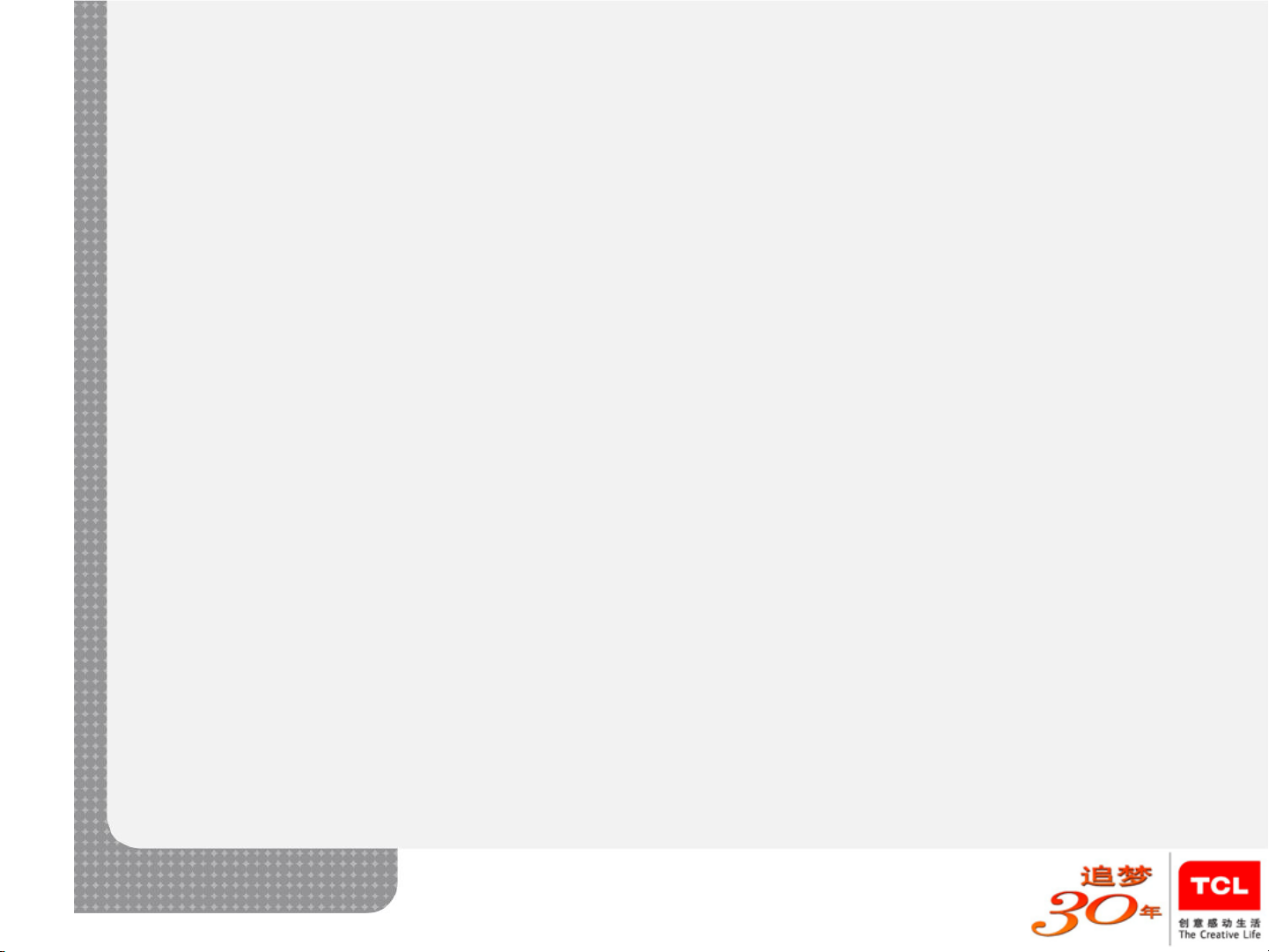
CCFL Lamps Appearance
U-shapes lamps
straight lamps
M-shapes lamps
Page 3
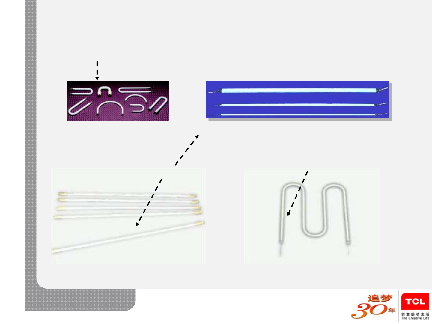
Inverter Board
Power supply voltage board and
inverter board is one PCB
Inverter board
Page 4
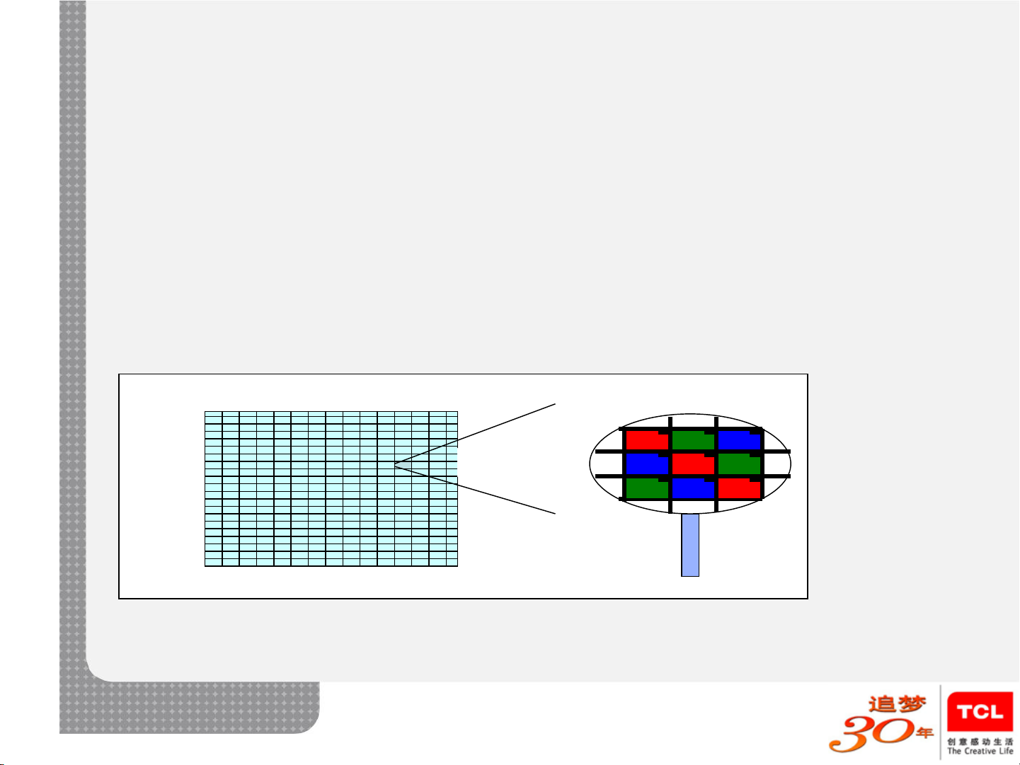
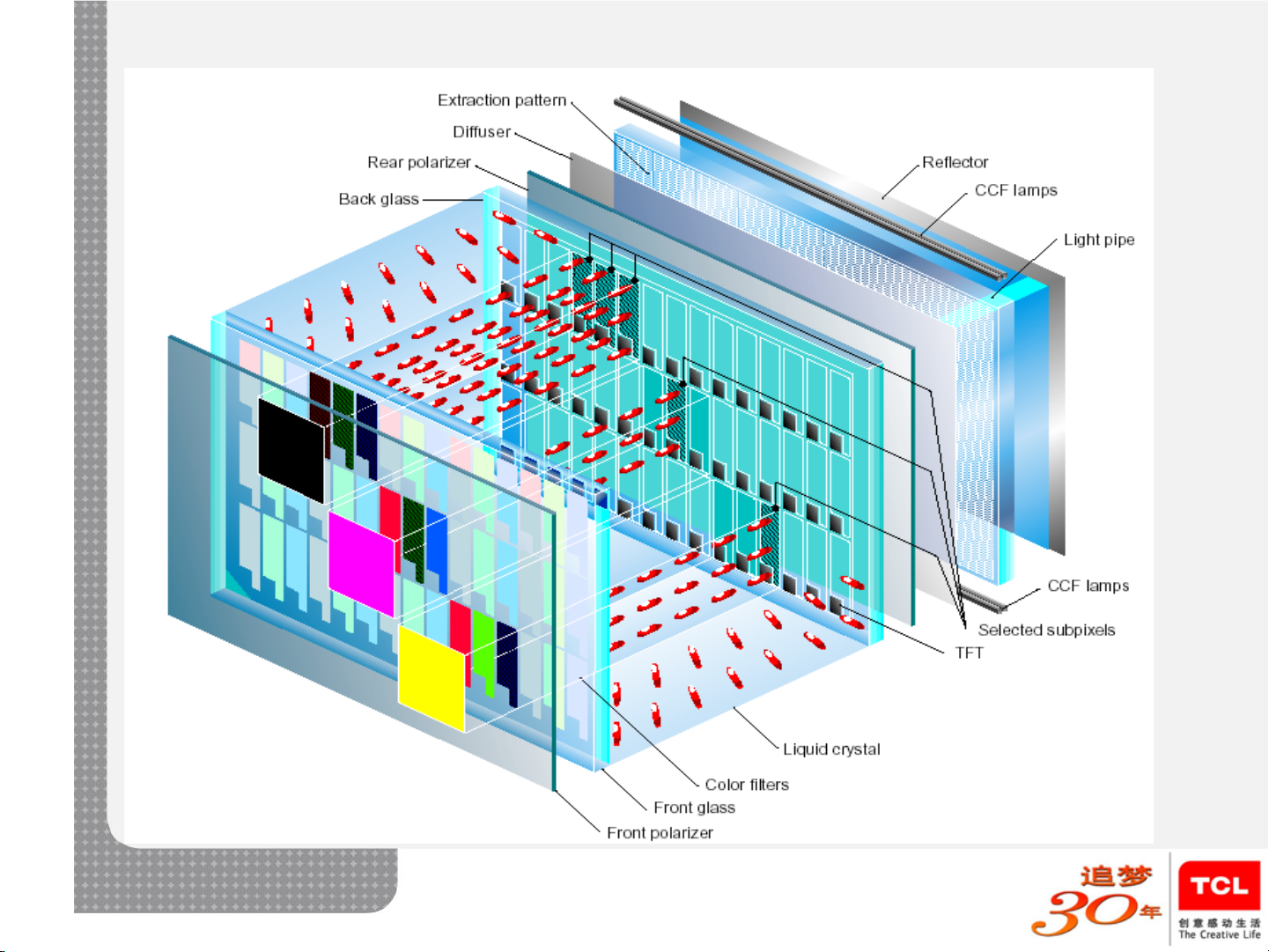
TFT-LCD Imaging Principle
1:Scan IC transmission signal
2:Driver IC transmission imaging control signal
3:When one sub-pixel cut-off, the sub-pixel cannot get light to show black.
4:If sub-pixel cut-off ,but light through the color filter and display color
5:After the synthesis of light effects, the display can produce color effects.
Color filter
enlarge
Page 5
TFT-LCD Imaging Principle
Page 6
TFT-LCD Imaging Principle
Page 7
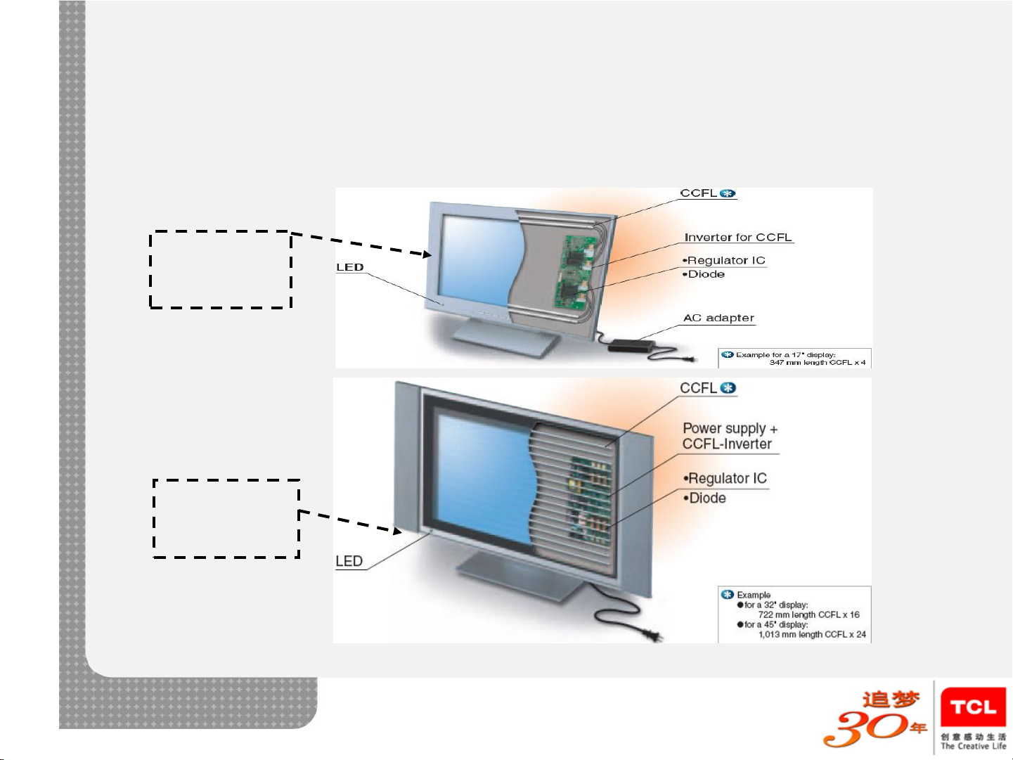
CCFL backlight LCD TV
4unit CCFL
small size
LCD TV
Lots of CCFL
big size LCD
TV
CCFL is not produce display signals , only provide light source.
Inverter board is a DC to AC converter. It is low-voltage DC convert into high-
voltage AC, and supply to light up CCFL lamps.
Page 8
CCFL Parameters
Parameter Symbol
Values
Unit
Min Type Max
Operating Voltage V
BL
655 685 805 V
RMS
Operating Current I
BL
3.0 5.0 6.0 mA
RMS
Starting Voltage(at 0 C)
Vs 1370 V
RMS
Operating Frequency F
BL
45 58 80 kHz
Power Consumption P
BL
3.43 3.77 Watt
Page 9
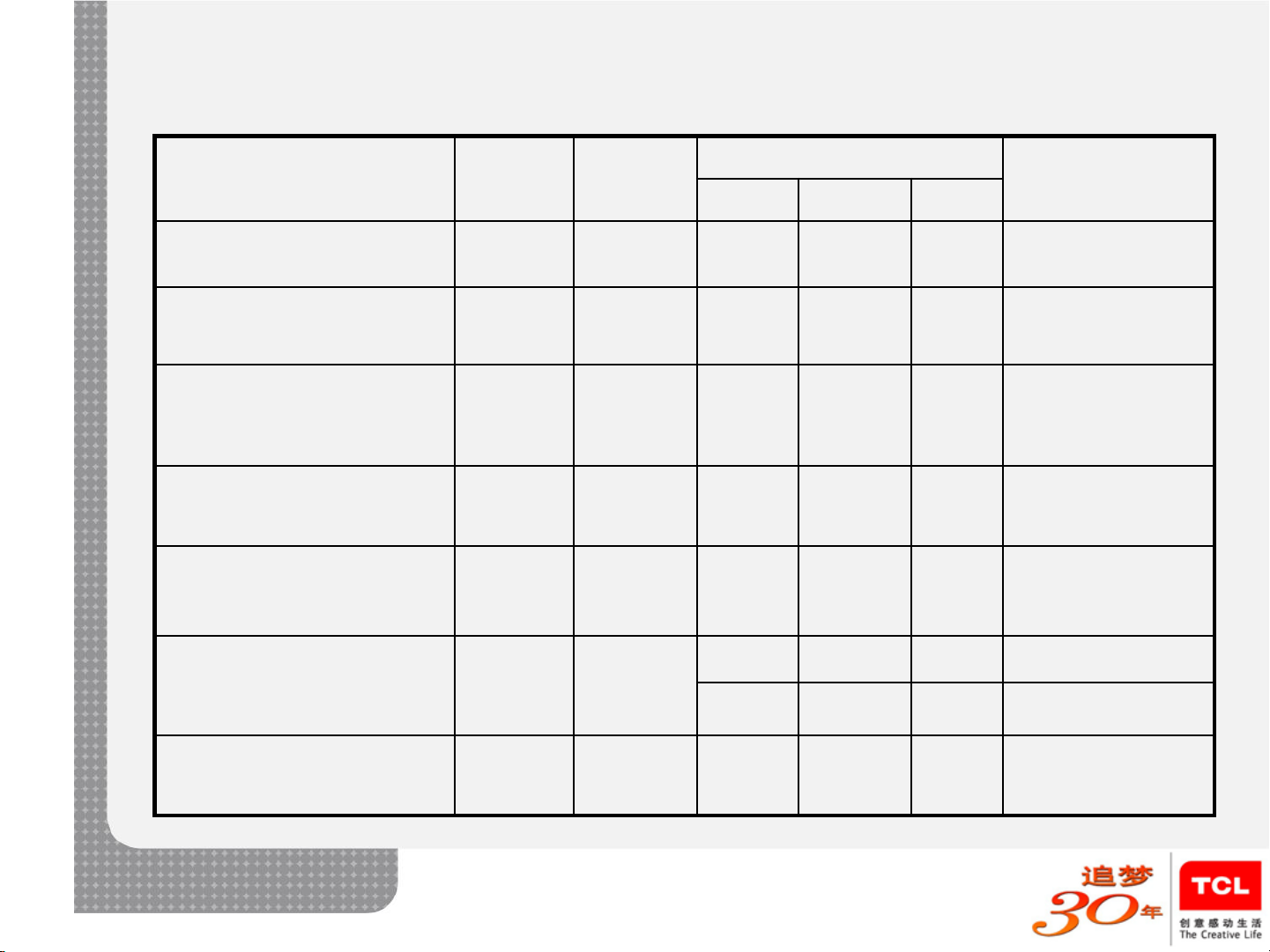
Inverter parameters(size:24)
Item symbol unit
value
remark
MIN TYP. MAX
输入电压input voltage
Vin V 9 12 16
工作频率operate
frequency
foper kHz 40 50 80
调光电压dimming
voltage
Vdim V 0 5 Anode or
cathode
dimming
灯管电流lamp current
Ilamp mArms 3.0 7.5 8.0
工作电压
Operating voltage
Vlamp Vrms 700 880 I lamp=7.5mA
启动电压
Start-up voltage
Vopen Vrms 1250 Ta = 25 ºC
1650 Ta = 0 ºC
启动时间start-up time
Ts S 1 3
Page 10
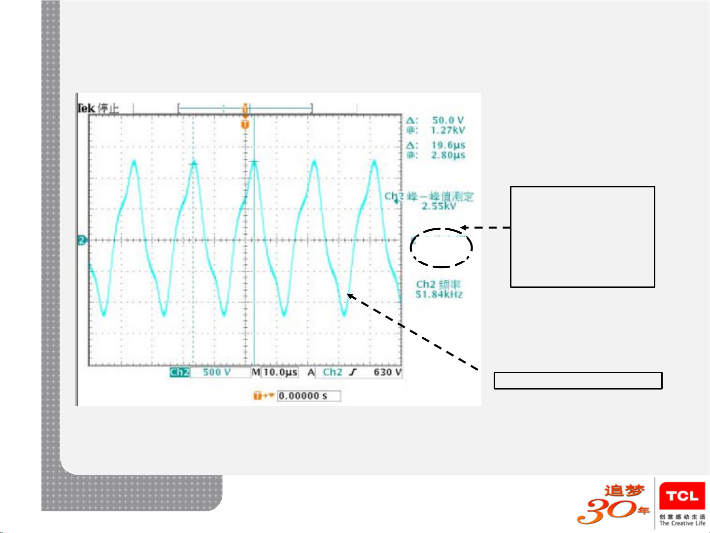
CCFL Operate Voltage Waveform
• CCFL lamp light, the
voltage drop large,
sine waveform change
some distortion
CCFL operate voltage
is 765V,normal CCFL
operate voltage is
600V---800V,start
voltage is as high as
1500V—1800V
Distortion sine waveform
765V
Page 11
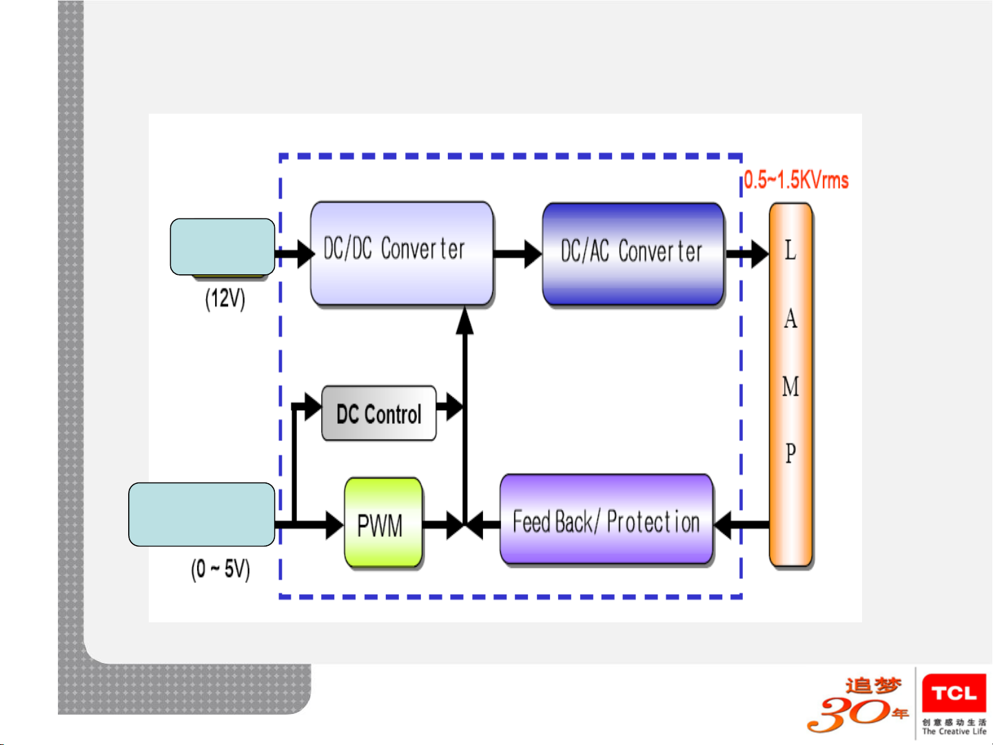
Block Inverter Diagram
Brightness
adjustment
Input
Page 12
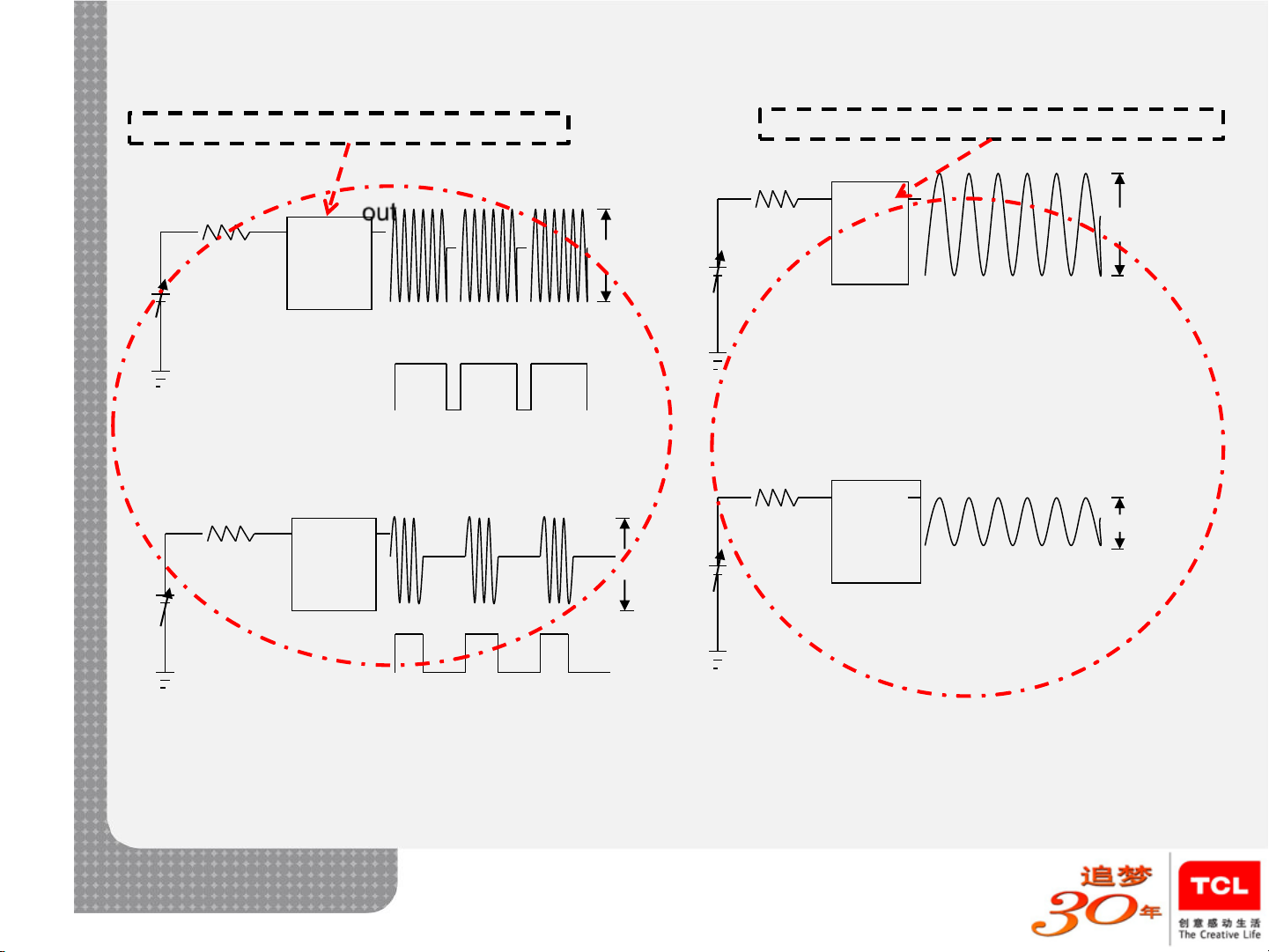
CCFL and LED Dimming
Imax
inverter
fb
Vadj out
Duty cycle regarding large dimming
fb
Vadj
inverter
out
Duty cycle regarding small dimming
Imax
LED dimming pricinple(PWM mode)
inverter
fbVadj
out
Imax
inverter
fbVadj
out
Imax
Duty cycle regarding large dimming
Duty cycle regarding small dimming
CCFL dimming pricinple(Analog mode)
Page 13
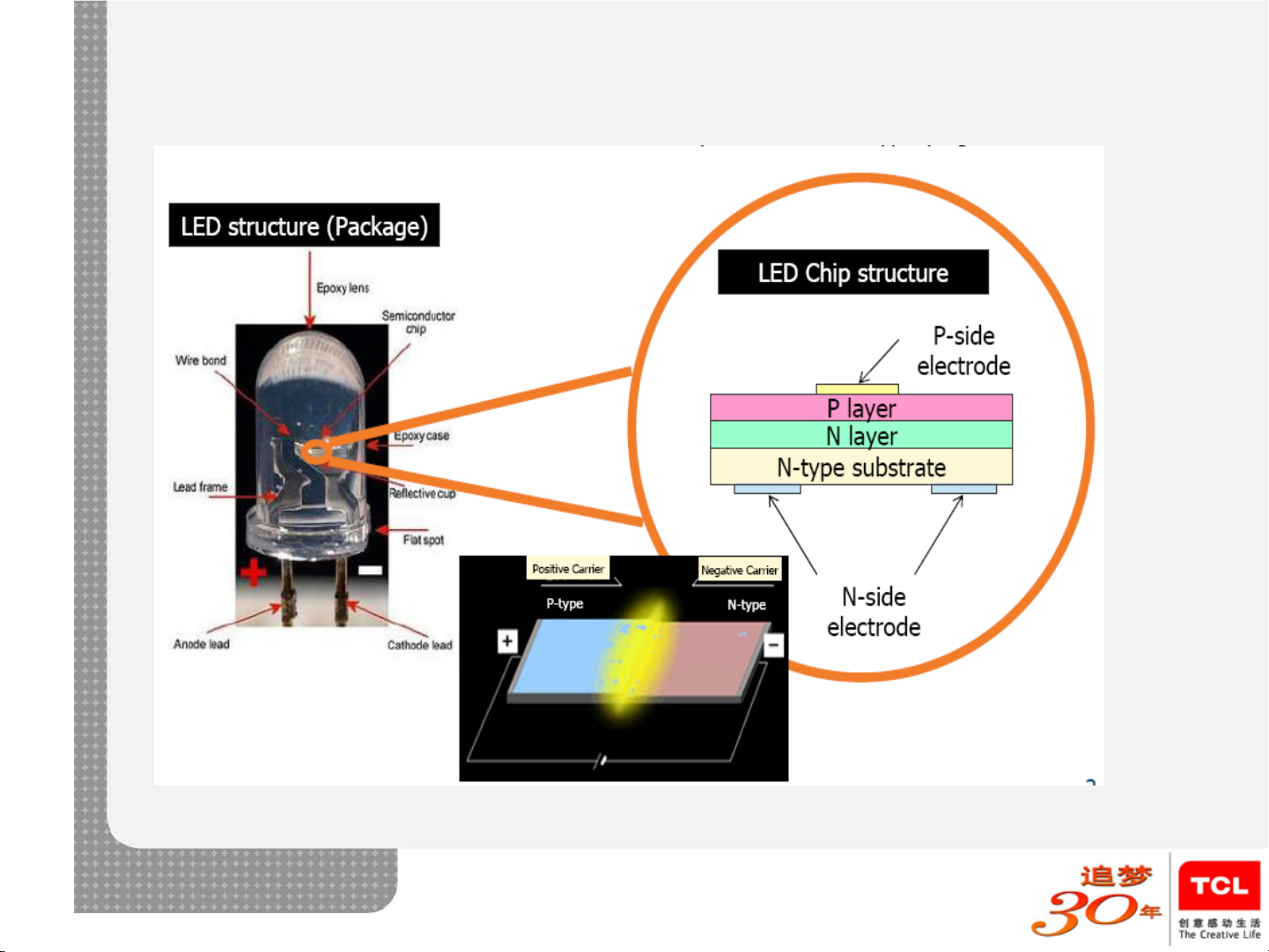
LED Chip Structure
Page 14
LED Chip Structure
Page 15
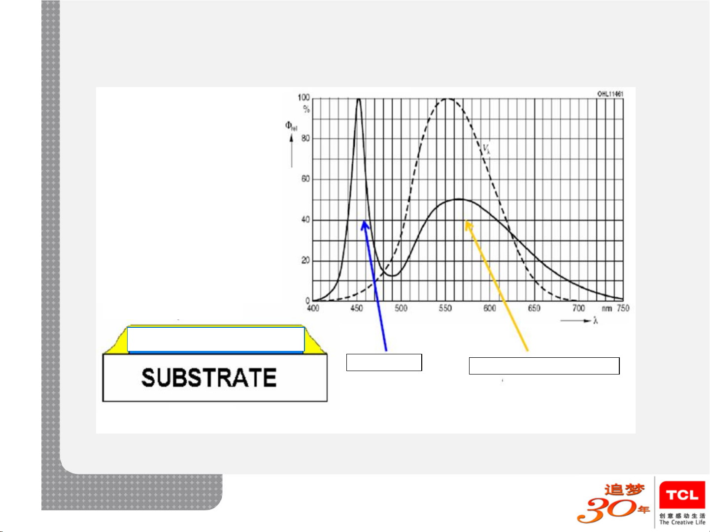
White LED structure
From phosphor layer
From LED
Large area phosphor layer
Page 16
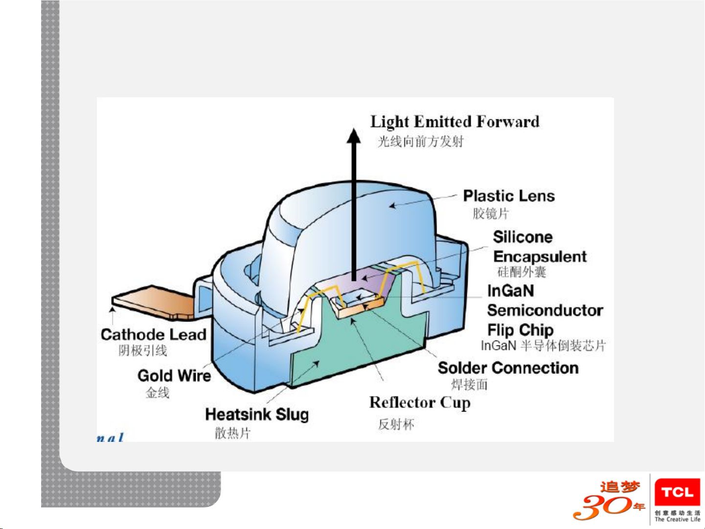
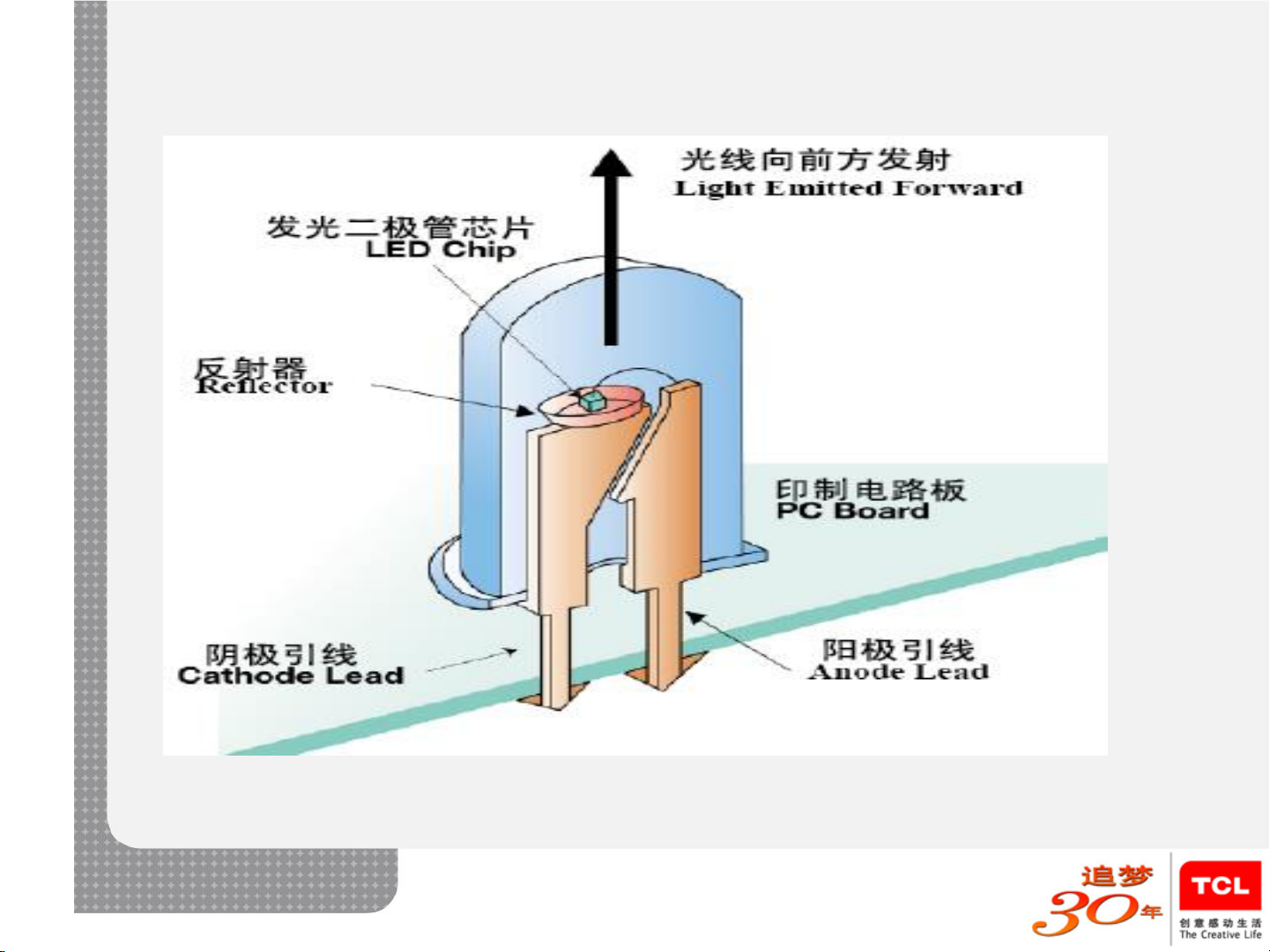
High Brightness LED Structure
Page 17
LED Advantages
•Low power consumption
• Extremely long lifetime
• Very low early failure rate
• Smallest
• Shockproof
• Does not produce UV radiation
Or intermediate frequency
interference
• Low power
• Light through the optical lens
transmitted out
• High color efficiency
•Low voltage
Page 18
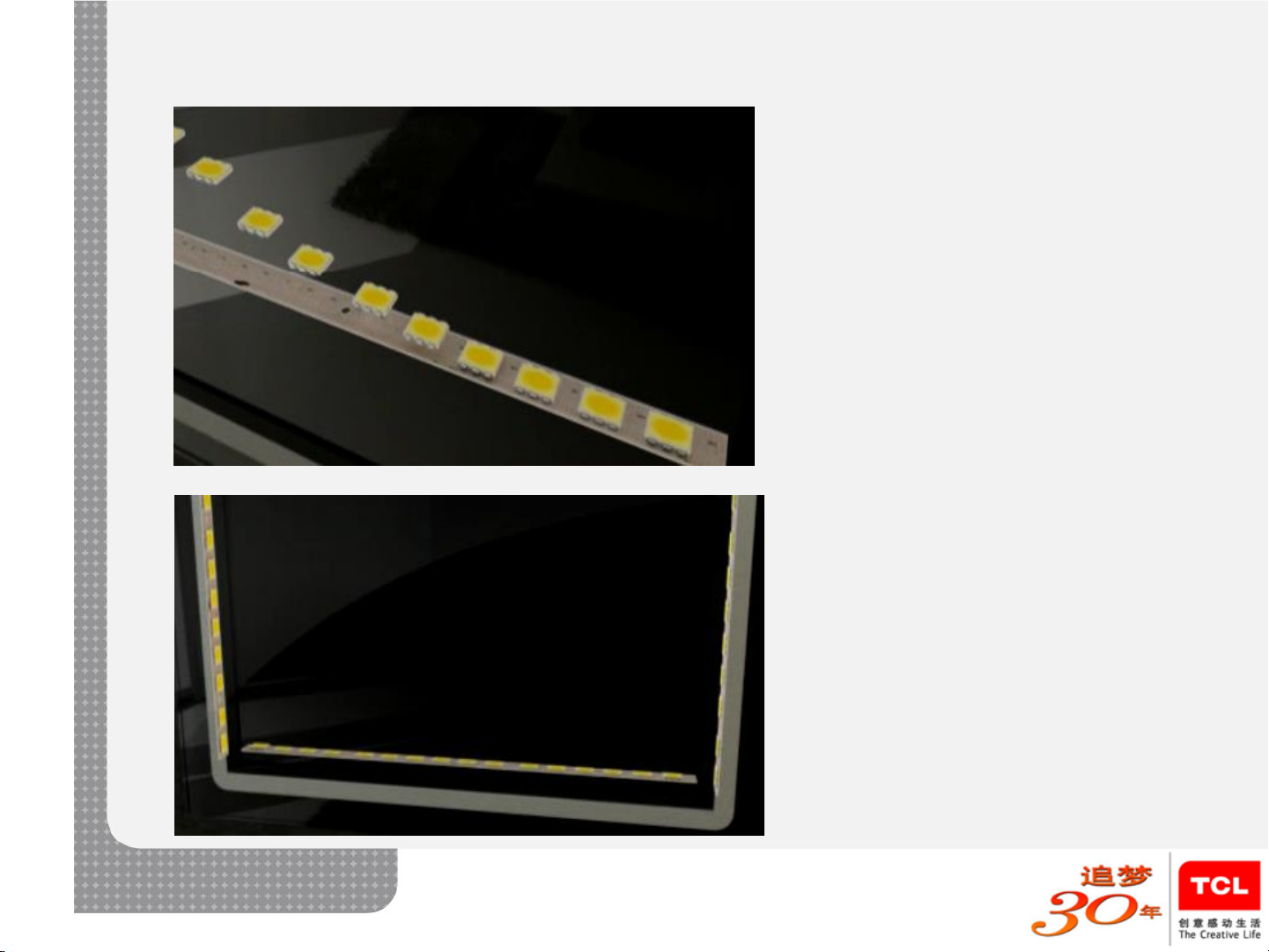
LED Bar of LED TV
•By a number of independent
white LED light strip solder into
the PCB (or aluminum plate)
Installed in the frame on the
screen (the side, both sides or
multilateral)
•Light of the length and the
number of LED lamps according
to the size of screen size varies
•The LED light on the many uses
of the series (some machines will
be used in parallel or seriesparallel hybrid) connected
•A single light on one or more
strings of LED
•Require specialized multi-string
LED constant current driver circuit
to drive
Page 19

LED TV Structure
Page 20

LED vs CCFL
• Brightness and the startup time
0.00
100.00
200.00
300.00
400.00
500.00
600.00
1 1723435146858561027119813691540171118822053
0.00
100.00
200.00
300.00
400.00
500.00
1 38 75112149186223260297334371408445482519556
CCFL
LED
Page 21

LED vs CCFL
Light remote control interference
CCFL Spectrum
LED Spectrum
Page 22

LED vs CCFL
CCFL:need additional start-up
high –voltage,stimulate mercury
vapor.
LED:The use of stable DC power
supply, no additional start-up highvoltage
Page 23

LED TV And LCD TV Differences
• LED TV and LCD TV's biggest difference is the different use of the backlight
• LCD TV uses CCFL (Cold Cathode Fluorescent Lamp) lamps, CCFL drawback is that lifetime
is short compared with LED and CCFL using raw materials containing mercury, mercury
pollution of the environment is a big injury
• LED TV: LED backlight that is used LED lamps. The disadvantage is higher the cost of LED
than CCFL , but lifetime is longer compared than the CCFL, and the mercury-free, less
environmental damage
CCFL
LED
Page 24

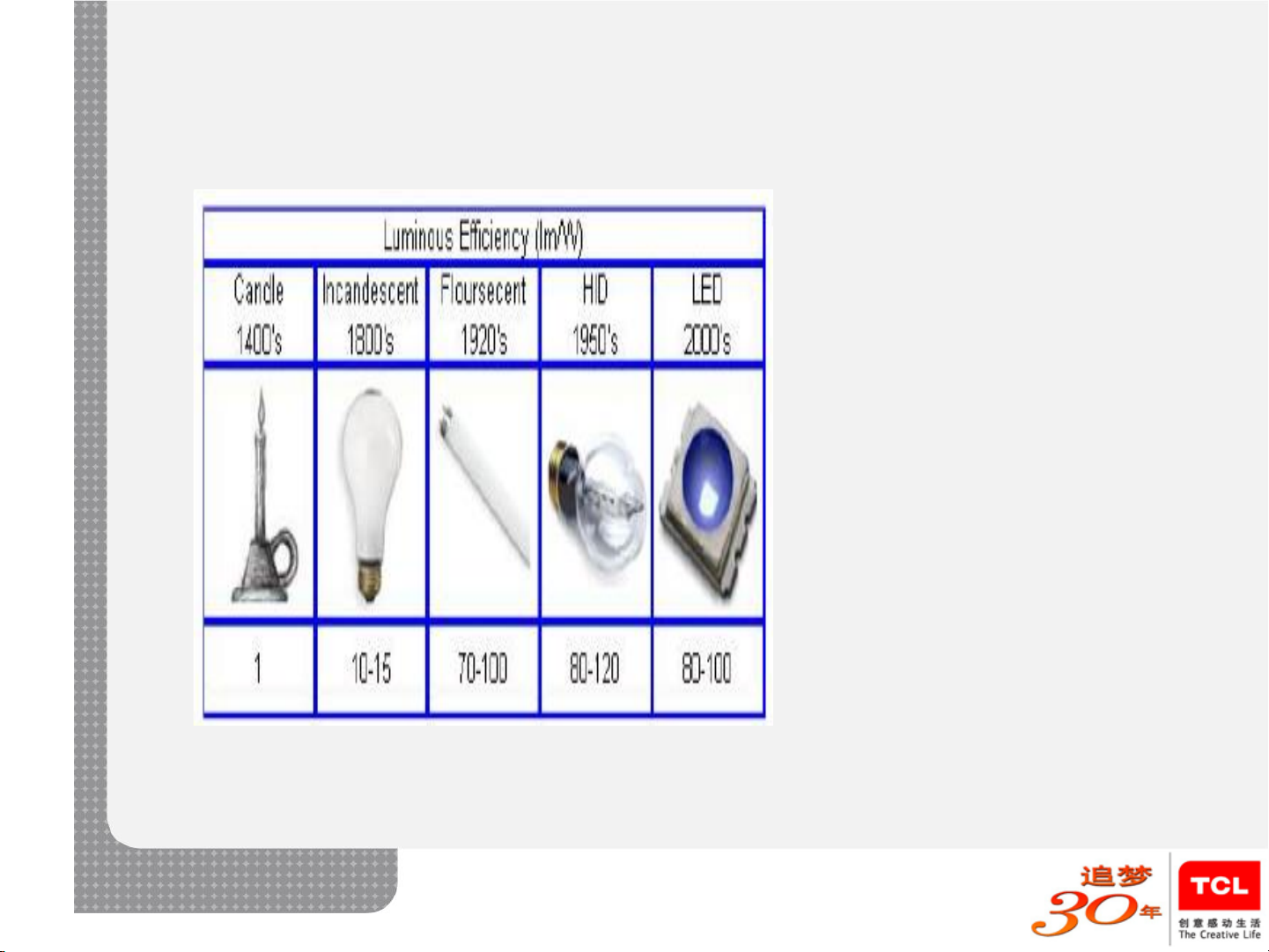
LED and CCFL Backlight Compare
• Environmental protection(Material does not contain mercury)
• Currently CCFL light efficiency of 60 to 100lm / w
• Currently LED light effect can be achieved about120lm / w
• Low power, Follow-up development can be achieved higher
• long lifetime(Up to 100,000 hours)
• support collor is very wide:excellent display color
• DC driver, Easy to dynamically adjust the brightness
• safety: CCFL high-voltage drivers, LED drivers only need low-voltage
• CCFL for the fragile glass products, LED chips for the semiconductor solid-state
Page 25

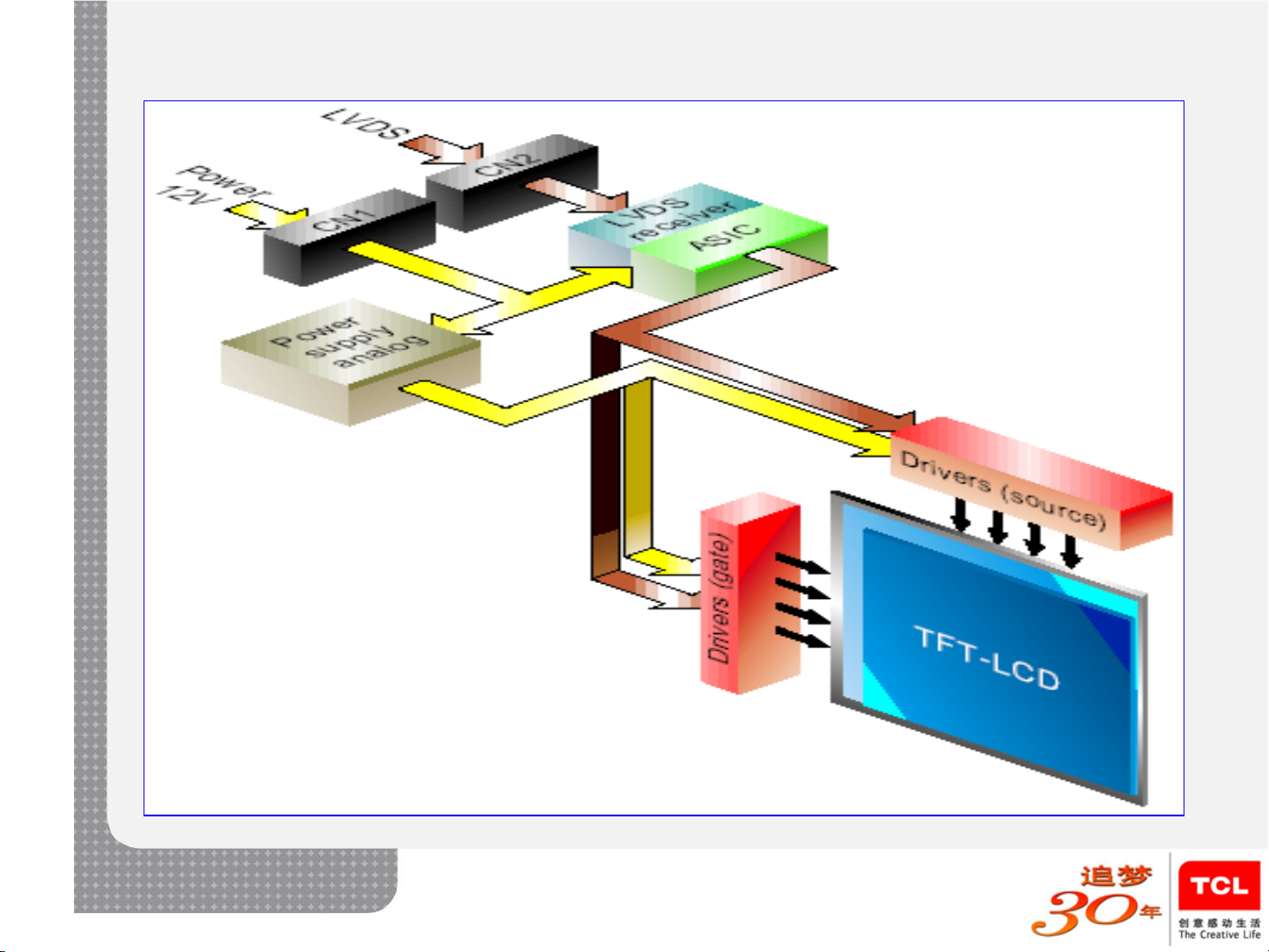
LCD Panel Block Diagram
Page 26

T-CON Board Introduction
Page 27

Inverter Board Introduction
Page 28

TFT-LCD Block Diagram
Power Converter
(DC/DC Converter)
Timing
Controller
Vcom
Gamma
Reference
Voltages
Source Drivers
Gate Drivers
TFT -LCD Panel
Data In
(LVDS)
Backlight
inverter
Lamps
Power
In
for
signal
Power In
for
Inverter
RSD
S
Page 29

Timing Controller
LVDS
Rx
ACC
DCC
Data
Controller
Memory
Controller
PLL
T-CON
RSDS
Rx
RSDS
Rx
SSC
EEPROM
Memory
(DDR)
L
V
D
S
T
x
Front
RSDS
Data
Back
RSDS
Data
ACC : Accurate Color Capture
DCC : Dynamic Capacitance
Compensation
Control Signal
&
Gate Signal
SSC : Spread Spectrum Clock
Input Signal
DE Mode Only
RGB 24bit Data
Clock
Page 30

LVDS Signal Input Data VESA JEIDA
RxIN0
RxOUT0 R0 R2
RxOUT1 R1 R3
RxOUT2 R2 R4
RxOUT3 R3 R5
RxOUT4 R4 R6
RxOUT6 R5 R7
RxOUT7 G0 G2
RxIN1
RxOUT8 G1 G3
RxOUT9 G2 G4
RxOUT12 G3 G5
RxOUT13 G4 G6
RxOUT14 G5 G7
RxOUT15 B0 B2
RxOUT18 B1 B3
RxIN2
RxOUT19 B2 B4
RxOUT20 B3 B5
RxOUT21 B4 B6
RxOUT22 B5 B7
RxOUT24 HSYNC HSYNC
RxOUT25 VSYNC VSYNC
RxOUT26 DE DE
RxIN3
RxOUT27 R6 R0
RxOUT5 R7 R1
RxOUT10 G6 G0
RxOUT11 G7 G1
RxOUT16 B6 B0
RxOUT17 B7 B1
RxOUT23
LVDS Signal Format
Page 31

Resolution Aspect Ratio No. of Pixel Panel Size
HD
15:9 1280 x 768 17”, 19”
16:9 1366 x 768 23”, 26”, 32”, 40”, 46”
FHD 16:9 1920 x 1080 40”, 46”, 5X”
Resolution of LCD TV
Page 32

Signal Item Symbol Min Typ Max Unit
Clock
Frequency
Fclk 60 80 85 MHz
Hsync Fh
43 50 53
KHz
Vsync Fv
48 60 66
Hz
Horizontal timing
Display
period
Thd -
1366
(1280)*
- Clocks
Total Th 1368 1600 1800 Clocks
Vertical timing
Display
period
Tvd - 768 - Lines
Total Tv 773 838 1200 Lines
Input Timing
Resolution : 1366 x 768
Page 33

LVDS Format Option
High : VESA, Low : JEIDA
No Signal No Signal
1 Vin(+5V) 11 GND
2 Vin(+5V) 12 Rclk3 Rx0- 13 Rclk+
4 Rx0+ 14 GND
5 GNN 15 Rx3-
6 Rx1- 16 Rx3+
7 Rx1+ 17 GND
8 GND 18 GND
9 Rx2- 19 LVDS Option
10 Rx2+ 20 N.C
Connector: DF14A-20P-1.25H(HIROSE) or Compatable
Model : 17”, 19”, 23” - HD
Input Pins Assignment
LVDS cable
Page 34

No Signal No Signal
1 N.C(#1) 16 GND
2 N.C(#2) 17 Rx33 N.C(#3) 18 Rx 3+
4 GND 19 GND
5 Rx0- 20 N.C(#4)
6 Rx0+ 21 LVDS Option
7 GND 22 N.C(#5)
8 Rx1- 23 GND
9 Rx1+ 24 GND
10 GND 25 GND
11 Rx2- 26 Vdd(+5Vdc)
12 Rx2+ 27 Vdd(+5Vdc)
13 GND 28 Vdd(+5Vdc)
14 RxCLK- 29 Vdd(+5Vdc)
15 RxCLK+ 30 Vdd(+5Vdc)
Input Pins Assignment
Connector: FI-E30S(JAE) or Compatible
Model : 23”, 26”, 32”, 40” - HD
LVDS Format Option
High : VESA, Low : JEIDA
LVDS cable
Page 35

Input Pin Assignment
Connector: FI-E30S(JAE) or
Compatable
Model : 40”, 46 - FHD
No Signal No Signal
1 Odd Rx0 - 16 Even Rx2 +
2 Odd Rx0 + 17 Even RxCLK 3 Odd Rx1 - 18 Even RxCLK +
4 Odd Rx1 + 19 Even Rx3 5 Odd Rx2 - 20 Even Rx3 +
6 Odd Rx2 + 21 Ground
7 Odd RxCLK - 22 Ground
8 Odd RxCLK + 23
Ground
9 Odd Rx3 - 24
Ground
10 Odd Rx3 + 25
Ground
11 Even Rx0 - 26 5V Input
12 Even Rx0 + 27 5V Input
13 Even Rx1 - 28
5V Input
14 Even Rx1 + 29
5V Input
15 Even Rx2 - 30
5V Input
LVDS Cable
Page 36

Connector : S14B-PH-SM3(JST) or Compatible
No Pin Name Pin Configuration
1 Vin Typ 24V
2 Vin Typ 24V
3 Vin Typ 24V
4 Vin Typ 24V
5 Vin Typ 24V
6 GND Ground
7 GND Ground
8 GND Ground
9 GND Ground
10 GND Ground
11 NC No Connection
12 B/L On/Off Inverter Enable
13 ADIM Analog Dimming
14 PDIM PWM Dimming
B/L On/Off
3.3V : On, 0V : Off
Analog Dimming
3.3V : Max, 0V : Min
PWM Dimming
Duty 30% : Min, Duty 100% : Max
Input Pin Assignment(Inverter)
Inverter cable
Page 37

19” 23” 26” 32” 40”
Lamp 6 U-Lamps 6 U-Lamps 8 U-Lamps 16 Lamps 20 Lamps
Input Voltage 24V 24V 24V 24V 24V
Output Current 4.5/~ /6.5 4.0/~ /7.0 4.5/5.5/6.5 4.0/5.5/7.0 4.0/5.5/7.0
PWM Dimming 30% 30% 30% 30% 30%
Analog Dimming O O O O O
PWM
Frequency
170Hz 170Hz 170Hz 170Hz 170Hz
Lamp Frequency 60KHz 60KHz 60KHz 60KHz 60KHz
Power
Consumption
50W 70W 80W 110W 180W
Inverter Specifications
Page 38

LED Backlight Driving Principle
Control Signal
Page 39

It is panel ( part NO.:LC420WUE-SBA) power sequence
LCD Driving Circuit
Page 40

It is panel ( part NO.:LC420WUE-SBA) power sequence
Power Sequence
Page 41

TCL 26D20 LED drive circuit
26D20—MP3389 is step-up control for 12 strings LED driver
DC=24V to
DC=12V
converter
24Vconverter 38V DC-DC
and Multi-channel constant
current control output
voltage
divider
resistor
backlight
ON/OFF
control
signal
PWM
dimmi
ng
signal
Page 42

MP3389’s Circuit
Page 43

Fromt mounting
bracket
Panel serial NO.
After taking out open
cell,we can see
protection sheet
Take
care
braket
1
2
3
4
protection sheet
prim sheet(vertical)
prim sheet(horizontal)
Diffuser sheet
Cable
LED Panel Structure Introduction
Front LCD PANEL
Inverter board
T-con
boar
d
Open cell
Source board
Take care Tape Carrier Package
CCFL’S
Socket
Page 44

LED Panel Structure Introduction
LED lamp
Inverter
board
Panel Serial NO.
T-CON
board
LED poower
supply socket
Front mounting bracket
Flexible printed cable
1
2
3
4
protection sheet
prim sheet(vertical)
prim sheet(horizontal)
Diffuser sheet
LED panel
Open cell
After taking out open cell,we
can see protection sheet
Page 45

Backlight Structure Introduction
Page 46

Power
supply
socket
Qty’s LED lamps:18 unit
Qty’s LED lamps:18 unit
Two LED modules are parallel
If Vinput=57V,Vone led=57/18=3.2v,so that one LED’s voltage is very low
For example:Part NO.: 4A-LCD32T-AUC panel,there are 36 LED lamp each LED unit
Two LED diodes,if one diode is defetive,the
other diode can keep LED to light,two diodes is
defetive,all LED cannot light
Solder on the PCB
LED Panel Module Introduction
Page 47

The Others Introduction
Front
cabinet
Panel
Power
supply
board
Main
board
Stand base
component
Rear
cabinet
Front
cabinet
Panel
Power
supply
board
Main
board
Rear
cabinet
Open cell
Backlight
module
Common LCD TV structure
The other LCD TV structure
Page 48

Gate TCP
Explain:1、Gate PCB and Source PCB and FPC in the Board
(FPC=Flexible Printed Cable ,PCB=Printed Circuit Board)
2、TCP=Tape Carrier Package
Open Cell Structure
Source TCP
Source PCB+Gate PCB
Page 49

Working Instruction of The Panel
CCFL bracket
Take care flexible
printed cable
Reflector sheet
Assembly CCFL
,take careCCFL
not breaking
Take care :ccfl
and socket
connect
Assembly protection
sheet\prim sheet(two
\diffuser sheet
Assembly protection
sheet\prim sheet
(two\diffuser sheet
Finishing
assemblying backliht
module
Connect ground cable
Bring open cell to assembly
Put the open cell on
the backlihgt module
Take care source
gate board
Assembly bracket
Check here it is ok or not
Check panel it is ok or not
Tool’s moving opencell
Page 50

LCD Trouble Shooting
Check power
supply V=24V or 12V
CCFL is not light
Check power
supply
board
Check backlight on/off
Check main board
Check backlihgt board
CCFL flash
Check backlight board
Check
Vblihgt-dimming
or dimming
Check main board
N
N
N
Y
Y
Y
Y
(1) (2)
N
Y
Check power
supply V=24V
Check power
supply board
N
N
Y
Check Vt-con?(power
supplyof T-con board
Vt-con)
Check Vtcon?(powersupply
of T-con board
Vt-con)
Page 51

LCD Trouble Shooting
Check power
supply V=24V or 12V
CCFL is light and
then not light
Check power
supply board
Check backlight on/off
Check main
board
Check backlight
board
check CCFL or
connect to
CCFL cable or
socket
checkCCFL
or cable
N
N
N
Y
Y
Y
Page 52

Replace
PWM IC
N
N
Y
Y
CCFL is light to
keep 2S,and then is
not light
Check CCFL socket
Check CCFL’S
socket or plug
Check transformer or
feedback circuit
Check transformer’s
voltage
Check OPV and
OPC’s circuit
N
Check transformer’s
feedback circuit
Check PWM’s
OPV
and feedback
circuit
Check MOS’S
circuit
and feedback
circuit
N
Y
Check
transformer
or capacitor
Y
Y
Check OPC’s
circuit
N
LCD Trouble Shooting
Page 53

High Speed
—
megabits/second (Mbps) through gigabits/second (Gbps)
Low Power
—
x3.5mA current loop/output
Low Noise
—
low demands on power/ground
—
radiated electric fields tend to cancel
Low Cost
—
pure CMOS implementations
What is LVDS?
picture
Page 54

Host
System
Graphic
Controller
T-con
CMOS/TTL CMOS/TTL
Data(LVDS)
Clock(LVDS)
LVDS Interface
Data 4pair + Clock 1pair = 10 line
CMOS/TTL Interface
Data 24 line
Control 3 line
Clock 1 line
CMOS/TTL Interface
Data 24 line
Control 3 line
Clock 1 line
LCD
Module
LVDS Tx
LVDS Rx
▶ LVDS(Low Voltage Differential Signaling)
- Interface between TV set and LCD module
- 340mV swing
- 7:1 Muxing
- 100 ohm R-Termination
- Reduce Data Bus Width
What is LVDS?
Page 55

LVDS Signal Mapping
Page 56

▶ RSDS( Reduced Swing Differential Signaling)
- Interface between T-con and Source Drive IC
- 200mV Swing
- 2:1 Muxing
- 100 ohm R-Termination
- Reduce Data Bus Width
Driver
TFT
-
LCD
PANEL
.
.
Row
Driver
Timing Control
Column
Driver
N
Column
Driver
N
Column
Driver
N
Source
Driver
N
Driver
N
Source
N
ONLY 24
Data Lines,
RSDS (200mV) @ 80MHz
Row
. . . . . . . .
RGB Data(RSDS)
Timing/
Control
Clock(RSDS)
RSDS
Tx
Timing
Controller
D0 D1
D0 D1 D0 D1 D0 D1 D0 D1
D2 D3
D2 D3 D2 D3 D2 D3 D2 D3
RSDS00
RSDS01
RSDSCLK
DIO
RSDS Signal Mapping
What is RSDS?
picture
Page 57

TFT—Thin Film Transistor
LCD—Liquid Crystal Display
CCFL---Cold Cathode Fluorescent Lamp
LED-----Light Emitting Diodes
HCFL -----Hot Cathode Fluorescent Lamp
FMB ------Front mounting bracket
FPC--------Flexible Printed Cable(It is the circuit that applies to printing circuit with LC driver IC
and COG circuit interface.)
TCP--------Tape Carrier Package
BLU --------Back Light Unit
CELL------- Cell( It is the panel of liquid crystal that fill into the micro meter gap formed by
combining two glasses substrates.)
Cell gap-----Cell Gap(It is the gap between ITO film on color filter substrate and TFT
substrate.The size of the gap affects the transmittance of LCD display substrate and response
time of liquid crystal.)
CF-----------Color Filter (In order for LCD to generate colors,there is a pattern with Red,Green
and Blue,which is one of the parts in the LC cell.Color filter is structured by 4 major
components:Black Matrix to block light, pattern to display colors,transparent protection film made
from protection pattern and transparent electrode film used for driver LC).
CIE chromaticity diagram--------- CIE chromaticity diagram shows the graph of 2 dimensional
color coordinate.On the XYZ color graph and X10Y10Z10 color graph,it uses x,y or x10y10 direct
coordinate,and they are called CIE1931 color graph or CIE 1964 color graph.It is also known as
xy or x10 y10 chromaticity diagram.
Appendix
Page 58

Appendix
COF-------Chip On Film(It is a simplified termof chip on film,which is a method of connecting
IC chip to the electrode terminal of flexible printed circuit board.The specialty of this IC
package method can thinner the flexible printed circuit board,which is about one third of
thickness of TCP.It also increases the reliability of the liquid crystal display module.The
current connecting processes used are:conductivity film,conductivity paste and eutectic
conjunction.)
COG-------Chip On Glass(It is a process of connecting electrode terminal of idisplay glass sub
strate and I/O of Driving IC directly to each other.The Driving IC must have bumping,and the
material used for liquid crystal substrate bumping is Au.The manufacturing process,which
uses ACF as its connecting material,is more matred.)
COP--------Chip On Plastic(It is a simplified term of Chip On Plastic,which is a method of
connecting IC chip to the electrode terminal of plastic substrate.It is used for setting the driver
IC onto the liquid crystal panel of plastic substrate.
Contrast ratio-----The ratio between the maximum and minmum brightness when the LC is
On/Off.The contrast changes with different viewing angles,and therefore,maximum contrast
ratio is used for display.Generally,STN is 10:1 and TFT is 100:1 for display.
Data line------It is the perpendicular wiring used in TFT substrate to transfer display
signals.Because it is connected with the Source electrode or Drain electrode on each pixel in
TFT,it is also known as Source line or Drain line.The width of the line is often between few um
to 10 um.
Page 59

Appendix
Driver IC-------It is the IC that drives the LCD.There two types of display matrix:Scanning
electrode(column electrode)Driver and Signal electrode(row electrode)Driver.The package of
driver changes from QFP to TCP.The Driver IC of poly-silicon LCD panel forms directly in the
display screen.
Gray scale----- Gray scale is for tuning the display between maximum and minimum
brightness.When digital signal is input to it,according to2,3,4,6 and 8 bit,there are 4,8,16,64
and 256 different gray levels.Analogue input can be used for infinity level tuning display.There
are two ways of gray scale:LCD driving voltage tuning and frame rate control.
LCD Driver--------LCD Driver is for driving LC panel circuit or IC.In matrix terms,it can be
differentiated into column electrode Driver and row electrode Driver.
Scanning line------It is the horizontal wiring line,which transfers signal to the gate electrode in
TFT board,It is also known as gate line.It also has the function to select horizontal
pixels.When the pixels are selected by the scanning line,the TFT is in a conductivity
status,and signals can be written into each pixel from Data line.The signal delay in the
scanning line causes great impact to the quality of the screen image,and therefore,low resisto
scanning line should be used.
 Loading...