

Page 1
SERVICE MANUAL
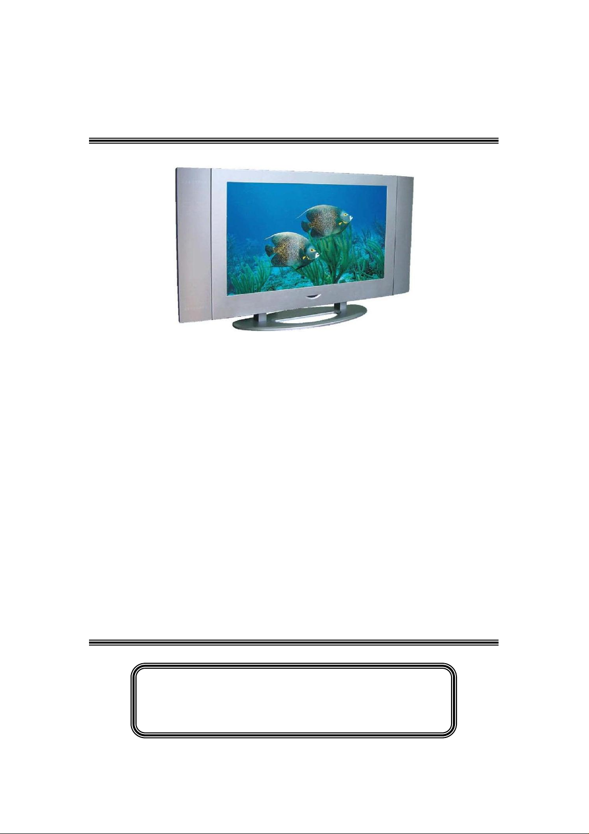
LCD2326LV
1. Caution………………………………………………….2
2. Specification…………………………………………….6
3. BOM List………………………………………………10
4. Alignment Procedure………………………………….18
5. Block Diagram………………………………………....24
6. Schematic Diagram……………………………………25
7. Explode View Diagram………………………………..39
This manual is the latest at the time of printing, and does not
include the modification which may be made after the printing, by
the constant improvement of product.
Page 2
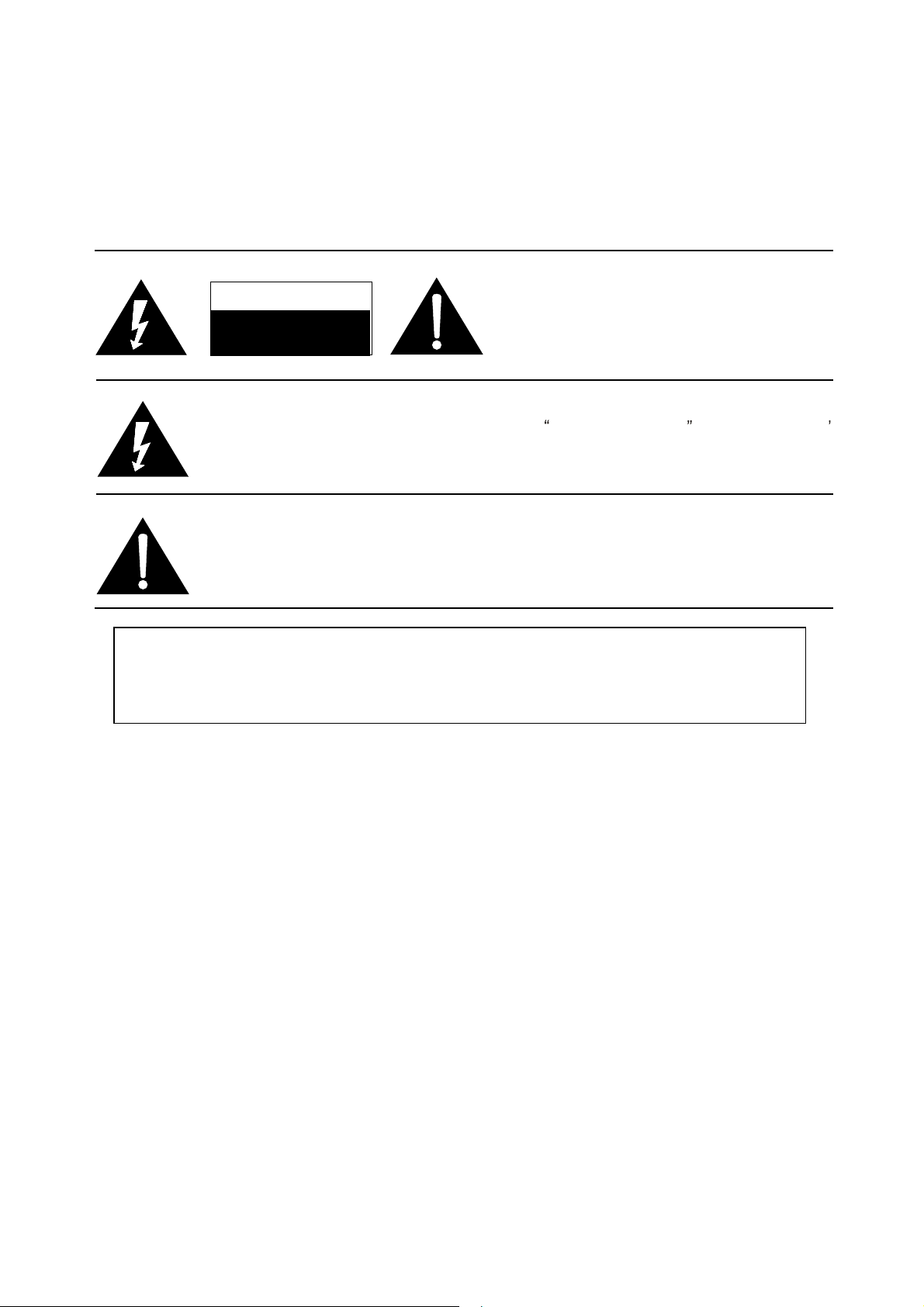
RISK
ELECTRI
SHOCK
NOT
OPEN.
SCHNEIDER ELECTRONICS GMBH-GERMANY
2
1. CAUTION
CAUTION:
Use of controls, adjustments or procedures other than those specified herein may result in
hazardous radiation exposure.
CA UT ION : TO RE DUCE THE RIS K OF
CA U T IO N
RISK
OF ELE CTR I
SHOCK
The lighting flash with arrowhead symbol, with an equilateral triangle is intended to
alert the user to the presence of uninsulated voltage within the products
enclosure that may be of sufficient magnitude to constitute a risk of electric shock to
the person.
The exclamation point within an equilateral triangle is intended to alert the user to the
presence of important operating and maintenance (servicing) instructions in the
literature accompanying the appliance.
DO NOT
C
OPEN.
ELECTR ICA L SHOC K, DO NOT REMOVE
COVER (OR BACK). NO USER SERVICEABLE
PAR TS INS IDE . RE FE R SER VIC ING T O
QUALIFIE D SERVIC E PERSONNEL.
dangerous
WARNING: TO REDUCE RISK OF FIRE OR ELECTRIC SHOCK, DO NOT
EXPOSE THIS APPLIANCE TO RAIN OR MOISTURE.
2
Page 3

SCHNEIDER ELECTRONICS GMBH-GERMANY
3
IMPORTANT SAFETY INSTRUCTIONS
CAUTION:
Read all of these instructions. Sa ve these instructions for later use . Follo w all W arnings and
Instructions marked on the audio equipment.
1. Read Instructions-All the safety and operating instructionsshouldbe read before the productis operated.
2. Retain Instructions- The safety and operating instructions should be retained for future reference.
3. Heed Warnings- All warnings on the product and in the operating instructions should be adhered to.
4. Follow Instructions- All operating and use instructions should be followed.
FOR YOUR PERSONAL SAFETY
1. When the power cord or plug is damaged or frayed, unplug this television set from the wall outlet and refer servicing to
qualified service personnel.
2. Do not overload wall outlets and extension cords as this can result in fire or electric shock.
3. Do not allow anything to rest on or roll over the power cord, and do not place the TV where power cord is subject to
traffic or abuse. This may result in a shock or fire hazard.
4. Do not attempt to service this television set yourself as opening or removing covers may expose you to dangerous
voltage or other hazards. Refer all servicing to qualified service personnel.
5. Never push objects of any kind into this television set through cabinet slots as they may touch dangerous voltage
points or short out parts that could result in a fire or electric shock. Never spill liquid of any kind on the television set.
6. If the television set has been dropped or the cabinet has been damaged, unplug this television set from the wall outlet
and refer servicing to qualified service personnel.
7. If liquid has been spilled into the television set, unplug this television set from the wall outlet and refer servicing to
qualified service personnel.
8. Do not subject your television set to impact of any kind. Be particularly careful not to damage the picture tube surface.
9. Unplug this television set from the wall outlet before cleaning. Do not use liquid cleaners or aerosol cleaners. Use a
damp cloth for cleaning.
10.1. Do not place this television set on an unstable cart, stand, or table. The television set may fall, causing serious injury
to a child or an adult, and serious damage to the appliance. Use only with a cart or stand recommended by the
manufacturer, or sold with the television set. Wall or shelf mounting should follow the manufacturer s instructions, and
should use a mounting kit approved by the manufacturer.
10.2. An appliance and cart combination should be moved with care. Quick stops, excessive force, and uneven surfaces
may cause the appliance and cart combination to overturn.
3
Page 4
SCHNEIDER ELECTRONICS GMBH-GERMANY
4
PROTECTION AND LOCATION OF YOUR SET
11. Do not use this television set near water ... for example, near a bathtub, washbowl, kitchen sink, or laundry tub, in a
wet basement, or near a swimming pool, etc.
Never expose the set to rain or water. If the set has been exposed to rain or water, unplug the set from the wall
outlet and refer servicing to qualified service personnel.
12. Choose a place where light (artificial or sunlight) does not shine directly on the screen.
13. Avoid dusty places, since piling up of dust inside TV chassis may cause failure of the set when high humidity persists.
14. The set has slots, or openings in the cabinet for ventilati on purposes, to provide reliable oper ation of the receiver, to
protect it from overheating. These openings must not be blocked or covered.
Never cover the slots or openings with cloth or other material.
Never block the bottom ventilation slots of the set by placing it on a bed, sofa, rug, etc.
Never place the set near or over a radiator or heat register.
Never place the set in enclosure, unless proper ventilation is provided.
a built-in
PROTECTION AND LOCATION OF YOUR SET
15.1. If an outside antenna is connected to the television set, be sure the antenna system is grounded so as to provide some
protection against voltage surges and built up static charges, Section 810 of the National Electrical Code, NFPA No.
70-1975, provides information with respect to proper grounding of the mast and supportingstructure, grounding of the
lead-in wire to an antenna discharge unit, size of grounding conductors, locationof antenna discharge unit, connection
to grounding electrode, and requirements for the grounding electrode.
EXAMPLE OF ANTENNA GROUNDING AS PER NATIONAL ELECTRICAL CODE INSTRUCTIONS
EXAMPLE OF ANTENNA GROUNDING AS PER
NATIONAL ELECTRICAL CODE
ANTENNA
LEAD- IN WIRE
GROUND CLAMP
ELECTRIC SERVICE
EQUIPMENT
NEC-NATIONAL ELECTRICAL CODE
ANTENNA DISCHARGE
UNIT (NEC SECTION
810-20)
GROUNDING
CONDUCTORS
(NECSECTION 810-21)
GROUND CLAMPS
POWER SERVICE GROUNDING
ELECTRODE SYSTEM
(NEC ART 250. PART H)
15.2. Note to CATV system installer : (Only for the television set with CATV reception)
This reminder is provided to call the CATV system attention to Article 820-40 of the NEC that provides
installer s
guidelines for proper grounding and, in particular, specifies that the cable ground shall be connected to the grounding
system of the building, as close to the point of cable entry as practical.
16. An outside antenna system shouldnot be located in the vicinity of overhead power lines or other electric lights or power
circuits, or where it can fall into such power lines or circuits. When installing an outside antenna system, extreme care
should be taken to keep from touching such power lines or circuits as contact with them might be fatal.
17. For added protection for this television set during a lightning storm, or when it is left unattended and unused for long
periods of time, unplug it from the wall outlet and disconnect the antenna. This will prevent damage due to lightning
and power-line surges.
4
Page 5

SCHNEIDER ELECTRONICS GMBH-GERMANY
5
OPERATION OF YOUR SET
18.
This television set should be operated only from the type of power source indicated on the marking label.If you are not
sure of the type of power supply at your home, consult your television dealer or local power company. For television
sets designed to operate from battery power, refer to the operating instructions.
19. If the television set does not operate normally by following the operating instructions, unplug this television set from the
wall outlet and refer servicing to qualifiedservice personnel. Adjust only those controls that are covered in the operating
instructions as improper adjustment of other controls may result in damage and will often require extensive work by a
qualified technician to restore the television set to normal operation.
20. When going on a holiday : If your television set is to remain unused for a period of time, for instance, when you go on
a holiday, turn the television set and unplug the television set from the wall outlet.
off
IF THE SET DOES NOT OPERATE PROPERLY
21. If youare unable to restore normaloperation by following the detailedprocedurein youroperating instructions,
do not attempt any further adjustment. Unplug the set and call your dealer or service technician.
22. Whenever the television set is damaged or fails, or a distinct change in performance indicates a need for
service, unplug the set and have it checked by a professional service technician.
23. It is normal for some TV sets to make occasional snapping or popping sounds, particularly when being
turned on or off. If the snapping or popping is continuous or frequent, unplug the set and consult your
dealer or service technician.
FOR SERVICE AND MODIFICATION
24. Do not use attachments not recommendedby the television set manufacturer as they may cause hazards.
25. When replacement parts are required,be sure the service technicianhas used replacementparts specified
by the manufacturer that have the same characteristics as the original part. Unauthorized substitutions
may result in fire, electric shock, or other hazards.
26. Upon completion of any ser vice or repairs to the television set, ask the service technician to perform
routine safety checks to determine that the television is in safe operating condition.
5
Page 6
p
p
g
e
s
q
z
prog
z
m
(2D)
y
(
)
(
)
(adj
)
2.Product Specification
6
Spec. and Features LCD2326LV
MasterData
Customer Id
Version
Status
Locked
12NC
Brand
EAN
UPC
Panel (1st design in TFT Panel)
supplier(1st design in, optional)
+Pixel Pitch
+Pixel Format
+Panel Format
+resolution 1280*768
+Brightness
+Contrast ratio
+View Angle
+Viewing Technology
+Response time
+back lights (CCFLx)
+panel interface
Life Time
Reception(TV)
+Tuning - presets/channels
+Tuning - technology
+Tuning - Indication
+Freq Bands
+Channels
+IF Freq
+TV Systems Off Air
+Add Systems Ext In
+TV Systems Multi
+Sound Systems
+Sound processing
Picture - Processing(TV/Video)
+Scan
+Scan Modes
+Wide Screen Switching
+BLACK STRETCH,BLUE STRETCH
+LTI; CTI
+Combfilter
+Deinterlace
+Picture Control
+Pict Enhancement
+Pict Noise Reduction coring
Macrovision support
Special features: JPEG Reader
Support USB connection
I-link(1394) capacity No
HDTV- Connection
+HDTV Ready: input: YPbPr/DVI YPbPr/DVI
+HDTV display: 1080i/720p
Picture - Display
+Display Type
+display aspect format
+Size(Visual)"
+Display output
Color Temperature
PC -connection
+Built-in PC display
?
0
cd
N
XX
LGP
0.3915mm X 0.3915mm
vertical stri
15:9
450cd/m2
400:1
Viewin
SIPS
16ms
X6
LVDS
50,000 hr
CCTV,CATV
PLL
fre
Full-Cable,UHF
45.75 MH
PAL-M/N, NTSC-M
PAL/NTSC
M, N
FM mono/stereo
Standard
4:3; 16:9wide screen; zoo
manual
Black strech, blue strech
-YES
memor
4 Picture Modes preset, and user adjustable:Brightness, Color,
Contrast, Tint, Sharpness
programmable peaking, dynamic stin tone control, Gama correction,
No.
No. ( Yes for new tooling: support added USB module)
1080i(60Hz)/720P
LCD-TFT
16:9 wide screen (default)
23"
8 bits digital RGB pixels driving
9300
YES
Angle Fre
./CH/Progrm position
-efficient deinterlace
Yes for new tooling: 6 in 1 JPEG Reader option
ustable
e RGB pixels
ressive 60h
a-si
Page 7
Spec. and Features LCD2326LV
p
g
n
(
)
t
g
e
yp
p
l
play
e
g
h
s
y
r
y
(
y
p
y
p
g
7
u
+input resolution:
+VGA input
+DVI input
+PC Synch
+PC Control
Sound
+speaker max. Power
+RMS Power output( Internal)
+RMS Power (External)
+Music Power output( Internal)
+DVSS(virtual Dolby Surround Sound)
+Surround Sound/BBE
+Sound Features
+Sound Control
+Sound effect design
Sound - Speakers
+Speaker configuration
+Speakers used
+Speaker Size
User Interface
+Interface Name
+Voice Control
+Menu
+Menu Colours
+Menu Languages
+Special Features
+Operational Features
to WXGA@60
YES
YES
auto w/"out of ran
DDC
5Wx2
2x2W
max.
2x4W
No(optional)
No/No(optional)
Mono/Stereo, psedo stereo, Smart Sound (AVL) , BTSC(optional)
Volume, Treble,Bass, Balance, 4 mode presets,
direct fron
2x1
Normal Ran
slim thin t
xx
No
bit ma
Multi-coloured On Screen Dis
en
sleep timer
power on/off; souce select; ch up/down; volume up/down; picture/sound
control; previous ch; menu enter/exit; mute;
icon/ highlight contro
lish,french,portugese,spanis
e" indicatio
e w/bass enhanc
e
for easy us
+PP Features
+Tuning/Install Features
+Clock/Timer Functions
+Local Controls Front
+Local Controls Top
+Local Controls bottom
+Indicators - screen
+Indicators - front
+Numb of Local Cont + Mains power
+Number of Ind. (incl Mains)
Remote Control
+Remote Control - scope
+Remote Control - type
+Remote Control - typenr
+Remote Control - features
Connectors Rear
+Scart RGB+Y/C+CVBS
+Scart RGB+CVBS in/out(full)
+Scart CVBS+Y/C
+Component In (Y/U/V) Cinch
+DVI In Cinch
+VGA In (RGB) Cinch
+PC audio In (%3.5)
+In Y/C+ Cinch(s-video+R/L)
+In Y/C (s-video)
+In CVBS Cinch(CVBS )
+In BNC (CVBS)
+In CVBS+Cinch(CVBS+R/L)
+In Cinch(CVBS+Mo)
+Out Cinch(CVBS+St)
+Out Cinch(CVBS)
One PP for all channel
- Plug & Play: Easiest Installation with optional direct station search or
menue-controlled search mode
- Automatic Tuning mode: all stations are stored incl. station name.
country-specific sorting will be done automatically. New stations can
be erased. CH fine Tuning: CH No. selection+frequency fine tuning.
24hours Timer on, Cr
--N/A
menu/volume up/down/+/-/source+ Power switch
es
LED
red): standb
6+1
1
TV, video,
Standard IR ,
Schneider's
TV,input selection,menu ,ch selection, volume, mute,etc.
--
--
-1
1
1
1
--1
---
--1
---
--#NAME?
anel displa
referin
stal Clock, Sleep time
Page 8
Spec. and Features LCD2326LV
(
)
pg
g
y
grey+p
p
9
v
z
ptor
5
g
g
e
(
)
8
+Out Cinch Audio Stereo
+Out Cinch Audio Mono
+Out Cinch Dolby Surround
+Power in Cinch
+Dig Audio Out
+Loudspeakers
+Control Busses
+Feature Slot
+ITV Smart Port
+Terr. Antenna in
Guide + IR Blaster Jack
Connectors Front
+In Cinch (CVBS + St)
+In Cinch (CVBS+Mo)
+Headphone Out
Connectors Side
+In Y/C + Cinch(CVBS+St)
+In Y/C + Cinch Stereo
+In Cinch (CVBS + St)
+IN Cinch (CVBS + Mo)
+Headphone Out
Connectors Top
Connectors bottom
+Headphone out
Connectors Mechanical
Styling
+Cabinet Name
+Configuration
+Graphics/Logo's
+Cabinet Colour and Finish
+Mechanics
+Speaker Visibility
General
+Segment
+Chassis
+Software Delivery Mode
+Software Version
+Mains Voltage
+Mains Frequency
+Type Mains Cord
Power Supply design
Power Consumption (P)TV in On
Power Consumption SB in Watts
Power Consumption Semi SB in W
+Power in "ON" for
+Power in Standby for
+Power in "OFF" for
Weight (P)TV (incl. Packaging)
Weight (P)TV (excl. Package)
Weight AVUnit excl Packaging
+INDICATION on BACKCOVER
+Channel
Final Equipment
+Packaging - methods
+Documents and manuals
+Languages DFU
+Cables Supplied
+Antenna Supplied
+Tuner detachable
+Stand Supplied
+wall mount bracket Supplied
+Aux Equipm Supplied
Packaging - width cm
Packaging - height cm
Packaging - depth cm
---
---
--1
DC in Jack
--internal
D-Sub 15 for S/W u
---
--75 Ohms (F type)
---
---
---
---
---
---
---
---
---
---
--1
smile
xx
spray metal logo
silver
Standard( internal)
Standard 16:
UOC-III-PW1306/8
reflashable
90-240
50/60H
VDE
external ada
110W
Less than
Rating Lable with power range Safety Warning Marks
2 Colour Printin
Yes
English(optional)
xx
n/a
Yes
stand detachabl
Yes
Batteries for RC
radin
c stri
, blue Carton, dismantled packin
2 x AA
Page 9
Spec. and Features LCD2326LV
y by
r
y by
r
y
(
g)
9
Miscellaneous
+EAN Indication
+Approbation
+Tests
+Local Integration
Various Perf. Param.
+Service Call-Rate
PIP/POP
+Type
+Features
Built-in Digital TV Reception
+ATSC Tuner
+DVB-S/C/T Tuner
+Transmission
Built-in Data System
+Text Standard
+(Tele)text Features
+Nbr bckgrnd page / Mem Size
+Text Technology
+Digital Data handling
+Program Guide
+CCD(close caption)
+CCD- V-chip
Built-in Clock/Timer
+Type
+Features
Built-in Radio
+Type
Built-in DVD drive
+Type of Medium
+Type of Deck
Phased Out Items
+Tuner/Frontend
+Sensitivity
+Lightning Protection
+Account
+XX(Radio Antenna in)
+Non Volatile Memory
+In Y/C + Cinch(CVBS+Mo)
Version of deck
Yes
CB
for assembl
for assembl
?
NO
---
--n/a
n/a
n/a
n/a
---
---
---
---
es
switchable
Yes
Timer on
0-24h
n/a
No.
n/a
Yes for new toolim
orde
orde
Page 10

3.Bom List
10
ITEM SPEC. QTY.
H3-2326AV-MX21 1
08-1726LA-DBY ASS'Y - DEBUG BD 1
33-KLN121-NTX CHIP BEAD 120 OHM +/-25% 9 FB701 FB702 FB703 FB704 FB705
FB706 FB707 FB708 FB709
40-1726LA-DBA2X P.C.B. BD 1
46-35199W-10X CONN. PH-10 10PIN PITCH=2.0mm 1 CN702
46-39409H-10X HS 10P 2468#26 120MM PH-10Y*2 1
47-VGA002-XX0 VGA JACKET D-SUB-15WP 1 CN701
08-1726LA-IRY ASS'Y - RECEIVE BD 1
02-IRR001-XX1 IR RECEIVER MODULE HRM380017 1 U511
11-SC1815-YBX TRANSISTOR 2SC1815Y 1 Q511
14-LED03R-XX1 LED RED Φ3MM FO203 1 D511
18-CB0101-JNX RES. C.F. 100 OHM 1/6W +/-5% 1 R511
18-CB0103-JNX RES. C.F. 10K OHM 1/6W +/-5% 1 R513
18-CB0202-JNX RES. C.F. 2K OHM 1/6W +/-5% 1 R512
18-CB0472-JNX RES. C.F. 4.7k OHM 1/6W +/-5% 2 R514 R515
25-BBB470-M1X CAP. ELEC 47 UF 10V +/-20% 1 C512
26-ABC104-ZFX CAP. CER 0.1 UF 50V +80-20% F 1 C513
40-1726LA-IRC1X P.C.B. IR RECEIVE BD 1
46-35135W-04X PIN BASE PH-04AW 1 CN511
LOCATION
08-2326LV-AVY ASS'Y - AV BD 1
18-CB0102-JNX RES. C.F. 1K OHM 1/6W +/-5% 2 R625 R626
18-CB0104-JNX RES. C.F. 100K OHM 1/6W +/-5% 2 R623 R624
18-CB0331-JNX RES. C.F. 330 OHM 1/6W +/-5% 2 R621 R622
25-BCB100-M1X CAP. ELEC 10 UF 16V +/-20% 2 C625 C626
26-ABC101-JZX CAP. CER 100 PF 50V +/-5% SL 4 C621 C622 C623 C624
35-LB1005-0IX FERR BEAD H75 (3.5X1X5) 1 FB621
35-LB1005-0IX FERR BEAD H75 (3.5X1X5) 1 FB622
40-2326LA-RCA1X P.C.B.BD 1
46-29002H-05X HS 5P24 F/W 90MM TJC3-5Y/SCN-5 1 CN622
47-RCA020-XX1 RCA SOCKET Y/W/R 1 CN621
08-2326LV-BSY 1
59-707720-00X RUBBER PAD 6
64-B40080-102 M/C SCREW B 4 X 8 4
64-Z40100-102 M/C SCREW B4 X 10 4
67-C70769-0A09A BRACKET 1
67-C70770-0A09A BASE 1
08-2326LV-FCN 1
42-04706D-XX0 SPEAKER 6 OHM 5W 2
46-27127H-02X HS 2P24 260/5 F/W TJC3-02H 1
46-35196H-02X HS 2P22 570/7 TJC3-2Y 1
4A-LCD23T-LG1 LCD LC230W01-A2 1
51-PC0220-0YU08 POWER CORD 1
54-392520-0X0 FIBRE WASHER 8 X 3 X 0.8 13 FOR IRON BRACKET & FRONT CABINET
54-719370-000 LENS PAD 1
Page 11

ITEM SPEC. QTY.
11
55-707550-3HA1A FRONT CABINET 1
56-707460-0HC1A LENS 1
56-707590-0HA1A PUSH BOTTON 1
56-707600-0HA1B POWER KNOB 1
57-10654X-00F TWIST TIE NY66 12
58-708810-0UI1A INLAY 1 FOR PUSH BUTTON
58-708840-1UI INSULATED SHEET 1
63-B30080-BT4 S/T SCREW B 3 X 8 BT 8 FOR SPEAKERS
63-B30080-BT4 S/T SCREW B 3 X 8 BT 3 FOR IR RECEIVER BD
63-B30080-BT4 S/T SCREW B 3 X 8 BT 3 FOR KEY BD
63-W30100-AB4 S/T SCREW W 3 X 10 AB 13 FIX IRON BRACKET TO FRONT CABINET
64-B30080-104 M/C SCREW B 3 X 8 2 40-1726LA-DBA2X & IRON BRACKET
64-B30080-104 M/C SCREW B 3 X 8 3 AV BD & IRON BRACKET
64-B30080-104 M/C SCREW B 3 X 8 2 POWER BD & IRON BRACKET
64-B30080-104 M/C SCREW B 3 X 8 4 MAIN BD & IRON BRACKET
64-B30100-104 M/C SCREW B 3 X 10 8 PANEL & IRON BRACKET
66-366850-6E2 STEEL NUT 2
67-M70766-2E0 BRACKET 1
67-S70767-2E0 SHIELD CAN 1
81-ADT245-421 AC ADAPTER 0227B24130 1
89-710370-JZ0 TAPE 66m 0.0250
LOCATION
08-2326LV-KEY ASS'Y - KEY BD 1
18-CB0471-JNX RES. C.F. 470 OHM 1/6W +/-5% 2 R501 R502
26-ABC104-ZFX CAP. CER 0.1 UF 50V +80-20% F 2 C504 C505
26-EBP103-ZFX CAP. CER 0.01UF 50V +80/-20% F 7 C506 C507 C508 C509 C510
C511 C512
40-1726LA-KED1X P.C.B. KEY BD 1
46-27626W-02X PIN BASE *2 TJC3-2A (HORIZON) 1 CN506
46-27626W-02X PIN BASE *2 TJC3-2A (HORIZON) 1 CN507
46-27626W-04X PIN BASE *4 TJC3-4AW 1 CN503
46-35135W-03X PIN BASE PH-03AW 1 CN504
46-35135W-04X PIN BASE PH-04AW 1 CN502
46-35135W-11X PIN BASE PH-11AW 1 CN501
46-39638H-11X 11P UL2464#26 350MM 1 FOR CN501
46-CC033T-04J 4P UL2468#26 330MM 1 FOR CN503
46-FF010F-04001 4P UL1185#26 100MM 1 FOR CN502
46-FF022T-03L HS 3P 2547#24 220mm PH-3Y 1 FOR CN504
47-EAR002-XX0 EARPHONE SOCKET CK3-3.5-9WK-B 1 CN505
48-POW022-XX0 POWER SUPPLY SWITCH PS2E-B 1 S507
48-TAC002-XX0 TACT SWITCH 1 S501
48-TAC002-XX0 TACT SWITCH 1 S502
48-TAC002-XX0 TACT SWITCH 1 S503
48-TAC002-XX0 TACT SWITCH 1 S504
48-TAC002-XX0 TACT SWITCH 1 S505
48-TAC002-XX0 TACT SWITCH 1 S506
08-2326LV-MAN 1
09-0BAV99-ATX HIGH SPEED DOUBLE DIODE BAV99 3 D6 D7 D8
09-BAV70L-ATX SMD. DIODE BAV70LT1(SOT-23) 215 2 D19 D3
09-LL4148-ATX SMD. SWITCHING DIODE LL4148 1 D22
Page 12

ITEM SPEC. QTY.
12
09-RLZ12B-DTX SMD. DIODE RLZ12B 1 D29
10-1N5820-F0X DIODE 1N5820 1 D28
11-0BC327-CBX TRANSISTOR BC327-40 2 Q1 Q2
12-BC847C-0BX SMD.TRANSISTOR BC847C 2 Q3 Q4
12-BT3904-0BX SMD. TRANSISTOR MMBT3904LT1(NPN) 9 Q12 Q15 Q18 Q19 Q27
Q31 Q34 Q35 Q36
12-BT3906-0BX SMD. TRANSISTOR MMBT3906LT1(PNP) 1 Q10
13-0024LC-21B IC 24LC21-SOIC8 2 U7 U9
13-0LM259-6SB IC LM2596(TO-263) 1 U18
13-1117MP-18B IC LM1117MPX-1.8 2 U30 U38
13-63LVDM-83B IC THC63LVDM83R 1 U17
13-74HC12-3DB IC 74HC123D 1 U11
13-EF4052-BTB IC HEF4052BT(D) 1 U16
13-EL1883-ISB IC EL1883 1 U10
13-IC1084-CMB IC AIC1084-33CM 3.3V (TO-263) 1 U37
13-LD1117-33B IC LD1117 3.3V 1 U28
13-LV800T-TCB 8M FLASH MX26LV800BTC-55 1 U4
13-M24C16-MNB IC 16K EEPROM M24C16-MN6 1 U12
13-M24C32-MNB IC M24C32-WMN6(S08) 1 U3
13-P12011-HDB01 IC TDA12011H/N1D01 1 U2
13-PI5V33-0QB IC PI5V330Q (QSOP) 2 U6 U8
13-PW1308-20B IC PW1308-20QL 1 U1
13-SI9953-DYB IC SI9953DY(8-PIN) 2 U29 U33
13-SN74HC-14B IC SN74HC14D-SOP14 1 U15
13-TDA151-7PP IC TDA1517P 1 U14
13-VC541A-00B IC 74LVC541A 1 U5
19-AB0000-JTX RES SMD 0 OHM 1/10W +/-5% 0603 12 R104 R105 R167 R168 R21
R239 R260 R27 R45 R46
R56 R64
19-AB0100-JTX RES SMD 10 OHM 1/10W +/-5% 8 R180 R181 R218 R36 R73
R74 R76 R77
19-AB0101-JTX RES SMD 100 OHM 1/10W 0603 21 R116 R125 R126 R127 R13
R131 R132 R135 R136 R14
R143 R15 R16 R163 R169
R18 R184 R231 R245 R246
R48
19-AB0102-JTX RES SMD 1K OHM 1/10W 0603 12 R112 R121 R133 R137 R189
R23 R24 R242 R26 R32
R38 R47
19-AB0103-JTX RES SMD 10K OHM 1/10W 0603 21 R147 R154 R155 R156 R170
R171 R182 R185 R203 R215
R232 R243 R247 R248 R251
R51 R54 R75 R78 R79
R81
19-AB0104-JTX SMD. RES 100K OHM 1/10W 0603 2 R205 R41
19-AB0105-JTX RES SMD 1M OHM 1/10W 0603 1 R40
19-AB0122-JTX SMD. RES 1.2K OHM 1/10 J 0603 3 R87 R88 R89
19-AB0123-JTX SMD. RES 12K OHM 1/10 J 0603 2 R35 R44
19-AB0155-JTX SMD. RES 1.5M OHM 1/10W +/-5% 0603 1 R20
19-AB0181-JTX SMD. RES 180 OHM 1/10W 0603 1 R172
19-AB0183-JTX SMD. RES 18K OHM 1/10W +/-5% 0603 1 R210
LOCATION
Page 13

ITEM SPEC. QTY.
13
19-AB0202-JTX SMD. RES 2K OHM 1/10W +/-5% 0603 1 R238
19-AB0221-JTX RES SMD 220 OHM 1/10W 0603 4 R141 R192 R94 R95
19-AB0222-JTX RES SMD 2.2K OHM 1/10W 0603 3 R202 R206 R209
19-AB0223-JTX SMD. RES 22K OHM 1/10W +/-5% 0603 1 R212
19-AB0229-JTX SMD. RES 2.2 OHM 1/10W J 0603 4 R49 R50 R52 R53
19-AB0270-JTX SMD. RES 27 OHM 1/10W +/-5% 0603 8 R148 R150 R151 R153 R157
R159 R160 R162
19-AB0273-JTX SMD. RES 27K OHM 1/10W +/-5% 1 R29
19-AB0274-JTX SMD. RES 270K OHM 1/10W +/-5% 0603 1 R166
19-AB0331-JTX RES. SMD 330 OHM 1/10W 0603 3 R96 R97 R98
19-AB0332-JTX SMD RES 3.3K OHM 1/10W 0603 25 R1 R17 R19 R2 R244
R249 R250 R252 R257 R258
R3 R4 R5 R71 R72
R8 R80 R83 R84 R85
R86 R9 R90 R92 R93
19-AB0391-JTX SMD RES 390 OHM 1/10W 0603 1 R33
19-AB0393-JTX SMD. RES 39K OHM 1/10W +/-5% 1 R39
19-AB0470-JTX RES SMD 47 OHM 1/10W +/-5%0603 2 R11 R12
19-AB0471-JTX SMD. RES 470 OHM 1/10W +/-5% 1 R241
19-AB0472-JTX RES SMD 4.7K OHM 1/10W 0603 11 R113 R123 R165 R186 R194
R222 R37 R57 R58 R6
R7
19-AB0473-JTX SMD. RES 47K OHM 1/10W 0603 4 R134 R139 R217 R34
19-AB0681-JTX SMD. RES. 680 OHM 1/10W 0603 2 R214 R31
19-AB0683-JTX RES SMD 68K OHM 1/10W 0603 1 R191
19-AB0750-JTX SMD. RES 75 OHM 1/10W 0603 15 FB28 FB31 R100 R101 R119
R128 R142 R144 R149 R152
R158 R161 R211 R216 R99
23-A08103-JBX NETWORK RES. 10K OHM +/-5% 0603 3 RN12 RN15 RN16
23-A08470-JBX CHIP ARRAY RES. 47 OHM +/-5% 0603*4 7 RN1 RN2 RN3 RN4 RN5
RN6 RN7
27-PBC223-J0X CAP. P.E 0.022 UF 63V +/-5% 2 C240 C241
28-AB0101-JCX SMD. CAP 100 pF 50VDC +/-5% 25 C100 C170 C171 C174 C175
C182 C183 C185 C186 C188
C189 C192 C193 C195 C196
C197 C198 C200 C201 C207
C208 C210 C211 C278 C99
28-AB0102-KBX SMD. CAP 1000 pF 50V +/-10% B 8 C12 C122 C15 C229 C263
C27 C6 C72
28-AB0103-ZFX CAP.SMD 10NF 50V +80-20% 0603 11 C271 C272 C275 C276 C277
C324 C325 C46 C48 C53
C84
28-AB0104-ZFX CAP. SMD 0.1UF 50V +80%~-20% F 132 C10 C101 C103 C105 C106
C109 C11 C111 C113 C114
C116 C118 C121 C126 C13
C131 C136 C137 C138 C14
C140 C142 C144 C147 C148
C150 C153 C157 C16 C18
C19 C2 C20 C204 C212
C213 C215 C218 C22 C220
C221 C225 C23 C231 C234
LOCATION
Page 14

ITEM SPEC. QTY.
14
C24 C243 C245 C247 C250
C253 C257 C259 C26 C267
C279 C283 C284 C285 C288
C290 C291 C294 C299 C30
C300 C301 C304 C306 C307
C308 C309 C31 C310 C311
C313 C314 C315 C316 C317
C32 C323 C327 C33 C331
C333 C336 C337 C339 C34
C342 C35 C350 C36 C37
C38 C39 C4 C40 C41
C42 C43 C47 C49 C50
C51 C52 C55 C56 C57
C58 C60 C61 C62 C64
C65 C68 C69 C70 C73
C75 C77 C78 C80 C81
C83 C85 C86 C90 C93
C96 C97
28-AB0120-JCX SMD. CAP 12 pF 50VDC 0603 +/-5% 3 C154 C155 C156
28-AB0180-JCX SMD. CAP 18 pF 50V +/-5% 0603 3 C139 C28 C29
28-AB0200-JCX CAP.SMD 20P 50V +/-5% 0603 3 C141 C145 C146
28-AB0223-ZFX CAP.SMD 0.022UF 50V 80-20 0603 1 C178
28-AB0224-ZFX CAP.SMD 0.22UF 50V +80-20%0603 14 C104 C108 C127 C128 C132
C244 C54 C59 C66 C76
C88 C89 C95 C98
28-AB0330-JCX SMD CAP 33PF 50V +/-5% 6 C191 C202 C203 C216 C222
C224
28-AB0333-ZFX CAP.SMD 0.033UF 50V 80-20 0603 1 C248
28-AB0334-ZFX CAP.SMD 0.33UF 50V 80-20 0603 1 C115
28-AB0392-KBX SMD. CAP 3900 PF 50VDC +/-10% 0603 1 C8
28-AB0393-ZFX SMD. CAP 0.039 UF 50V +80%-20% 1 C9
28-AB0473-ZFX SMD CAP 0.047 UF 50V +80-20% 4 C1 C230 C5 C7
28-AB0681-JCX SMD. CAP 680 pF 50V +/-5% 0603 2 C261 C268
28-AB0682-KBX SMD. CAP 6800pF 50VDC +/-10% 1 C120
28-RA0107-MAH SMD. CAP 100 UF 10V +/-20% 19 C107 C117 C125 C206 C286
C289 C3 C302 C305 C318
C332 C334 C335 C338 C340
C341 C63 C82 C94
28-RA0476-MAH SMD. CAP 47 UF 10V +/-20% 4 C233 C239 C258 C71
28-RC0105-MAH SMD. CAP 1 UF 16V +/-20% 5 C187 C209 C242 C251 C296
28-RC0106-MAX SMD. CAP 10 UF 16V +/-20% 25 C102 C110 C112 C130 C143
C149 C17 C205 C21 C214
C219 C232 C25 C260 C270
C273 C274 C287 C303 C312
C44 C45 C74 C79 C87
28-RC0107-MAH SMD. CAP 100 UF 16V +/-20% 5 C265 C280 C293 C298 C326
28-RC0225-MAH SMD. CAP 2.2 UF 16V +/-20% 13 C119 C168 C169 C179 C180
C181 C184 C190 C194 C199
C256 C91 C92
28-RC0226-MAH SMD. CAP 22 UF 16V +/-20% 1 C282
28-RD0227-MAX ALUMINIUM CAP. 220 UF 25V +/-20% 5 C246 C249 C255 C295 C67
LOCATION
Page 15

ITEM SPEC. QTY.
15
28-RD0337-MAF1 ALUMINIUM CAP.330 UF 25V +/-20% 1 C297
33-ELN190-NTX CHIP BEAD 19 OHM +/-25% 38 FB1 FB10 FB11 FB12 FB13
FB14 FB15 FB16 FB17 FB18
FB19 FB2 FB20 FB21 FB22
FB23 FB24 FB25 FB26 FB3
FB4 FB5 FB51 FB54 FB55
FB56 FB59 FB6 FB60 FB61
FB64 FB66 FB7 FB75 FB8
FB84 FB86 FB9
33-GLN100-NTX CHIP BEAD 10 OHM +/-25% 12 FB57 FB58 FB65 FB67 FB69
FB70 FB71 FB74 FB77 FB78
FB79 L3
33-KLN121-NTX CHIP BEAD 120 OHM +/-25% 15 FB27 FB30 FB32 FB33 FB38
FB39 FB41 FB43 FB44 FB46
FB47 FB48 FB49 FB52 FB53
36-LIF027-XX0 LINE FILTER LC-33A-TCL 1 L2
40-2026LA-MAC4X P.C.B. MAIN BD 1
41-WJ0075-B00 WIRE BARE JUMPER 7.5MM 3 J32 J33 J36
43-SFSS11-2DM RELAY SF-SS-112DM 1 RELA1
45-OSC14M-3Y2 CRYSTAL 14.31818MHZ 1 Y1
45-OSC24M-5N0 CRYSTAL 24.576 MHZ 1 Y2
45-SAW937-0M0 SAW FILTER M9370M 1 T2
45-SAWF18-590 SAW FILTER F1859 1 T1
46-27626W-04X PIN BASE *4 TJC3-4AW 1 CN14
46-27626W-05X PIN BASE *5 TJC3-5AW 1 CN11
46-33333W-04X PIN BASE VH-AW 1 CN25
46-35135W-08X PIN BASE PH-08AW 1 CN18
46-35135W-10X PIN BASE 10P 1 CN1
46-35135W-11X PIN BASE PH-11AW 1 CN13
46-35135W-11X PIN BASE PH-11AW 1 CN6
46-35199W-03X PIN BASE *3 PITCH=2.0MM 1 CN20
46-35199W-07X CONN.PH-7A PITCH=2.0MM 7PIN 1 CN23
46-39000W-20X PIN BASE DF14-20P(WF) 1.25PITCH 1 CN16
46-39409H-10X HS 10P 2468#26 120MM PH-10Y*2 1 FOR CN1
46-39637H-20X 20P UL1571#30 180MM 1 FOR CN16
46-FF012F-12K HS 8P UL2468#26 PH-8Y/12Y L=120 1 FOR CN8
46-KK018F-04T01 4P UL1015#22 180MM 1 FOR CN25
47-DVI001-KX0 DVI SOCKET KL-DIV024-04A 1 CN12
47-EAR005-XX0 EARPHONE SOCKET CK3-3.5-3WK-E 1 CN10
47-PWS012-XX0 SOCKET DSW-47 1 CN19
47-RCA020-XX1 RCA SOCKET Y/W/R 1 CN9
47-RCA125-XX0 RCA SOCKET RCA-3308D4-090 1 CN21
47-SVI008-XX1 SOCKET DSW-506WT-L 1 CN8
47-VGA002-XX0 VGA JACKET D-SUB-15WP 1 CN22
50-05000D-NUU FUSE 5A 250VAC 1 F1
50-05000D-NUU FUSE 5A 250VAC 1 F2
LOCATION
08-2326LV-PAN 1
06-515W31-A001X REMOTE CONTROL RC1523102/00 1
49-204260-BAT 7# BATT. UM4 R03P SIZE AAA 2
68-712200-001 LCD TV HANG RACK 1
Page 16

ITEM SPEC. QTY.
16
72-2326SV-E001A OPERATION MANUAL 1
74-026035-6WE1A POLYBAG 1
74-090070-5WD1A POLYBAG (90CMX60CMX0.5MM) 1
75-707740-CC2 POLYFOAM 1
75-707750-CC2 POLYFOAM 1
75-707950-CC2 POLYFOAM 1
75-707960-CC2 POLYFOAM 1
76-2326AT-0AT CARTON BOX 1
76-708830-0BT CARTON BOX 1
89-343400-000 PELLICLE (450mX450mmX0.018mm) 0.7000
08-2326LV-PWY 1
09-LL4148-ATX SMD. SWITCHING DIODE LL4148 4 D2 D3 D4 D5
09-RLZ12B-DTX SMD. DIODE RLZ12B 1 D1
12-BT3904-0BX SMD. TRANSISTOR MMBT3904LT1(NPN) 1 Q4
12-BT3946-0BX SMD TRANSISTOR MBT3946OW1T1G 1 Q6
12-D40N03-0BX MOSFSET NTD40 NO3RG 1 Q2
12-LR7807-0BX MOSFET IRLR7807Z 1 Q1
12-S7002A-0BX TRANSISTOR NDS7002A 2 Q3 Q5
13-CS5211-G0B IC CS5211G 1 U1
19-BB0103-JTX SMD. RES 10k OHM 1/10W +/-5% 2 R2 R7
19-BB0104-JTX SMD. RES 100k OHM 1/10W +/-5% 0805 1 R11
19-BB0109-JTX SMD. RES 1 OHM 1/10W +/-5% 0805 3 R12 R15 R8
19-BB0202-JTX SMD. RES 2k OHM 1/10W +/-5% 0805 1 R10
19-BB0221-JTX SMD. RES 220 OHM 1/10W +/-5% 0805 3 R3 R5 R6
19-BB0223-JTX SMD. RES 22k OHM 1/10W +/-5% 1 R9
19-BB0472-JTX SMD. RES 4.7k OHM 1/10W +/-5% 1 R1
19-BB0513-JTX SMD. RES 51k OHM 1/10W +/-5% 1 R4
28-BB0101-JCX SMD CAP. 100 PF 50V C 0805 1 C8
28-BB0104-ZFX SMD CAP. 0.1 UF 50V +80/-20% 0805 2 C4 C5
28-BB0105-ZFX SMD. CAP 1UF 50V +80%-20% 1 C2
28-RC0106-MAF SMD. CAP 10 UF 16V +/-20% 1 C3
28-RD0477-MAF ALUMINIUM CAP. 470 UF 25V +/-20% 1 C6
28-RE0477-MAF SMD. CAP. 470UF 35V +/-20% 1 C1
33-GLN121-NTX CHIP BEAD 120 OHM +/-25% 2 FB1 FB2
33-PLL150-MBX SMD.COLL L1207-150 1 L1
36-LIF077-XX0 LINE FILTER LH-0904 1 CT1
36-WID130-HX0 COIL WIDTH 13 UH +/-15% 1 L2
40-2326WS-PWC2X P.C.B. POWER BD 1
41-WJ0025-B00 WIRE BARE JUMPER 2.5mm 1 J2
46-33333W-04X PIN BASE VH-AW 1 J1
LOCATION
08-2326LV-RCN 1
54-114000-00X01 FELT TAPE 20
54-710350-00X02 FELT TAPE 1
54-710360-00X02 FELT TAPE 1
55-707560-3UA1A REAR CABINET 1
58-2326MP-0UI1H PLATE MODEL NO. 1
62-707580-0HA1C TUNER COVER 1
62-707610-0HA1C HINGE COVER (WITH AXES) 1
62-707610-1HA1C HINGE COVER (WITHOUT AXES) 1
Page 17

ITEM SPEC. QTY.
17
62-719410-0HA1A THE END AV BRACKET 1
63-B30120-AB3 S/T SCREW B 3.0 X 12 4 FOR FRONT & REAR CABINET
63-W30100-AB4 S/T SCREW W 3 X 10 AB 4 FIX AXES SUPPORT TO REAR CABINET
63-W30100-AB4 S/T SCREW W 3 X 10 AB 3 FIX WALL BRACKET TO REAR CABINET
64-B30060-103 M/C SCREW B 3 X 6 3 FIX REAR CABINET TO IRON BRACKET
64-B30080-103 M/C SCREW 3.0 X 8.0 1 FIX TUNER COVER TO REAR CABINET
64-B30080-104 M/C SCREW B 3 X 8 3 FIX TUNER BD TO IRON BRACKET
64-B30100-103 M/C SCREW B 3 X 10 2 FOR REAR CABINET
64-B40080-102 M/C SCREW B 4 X 8 4 FIX TURNING AXES TO REAR CABINET
64-F30060-103 M/C SCREW F 3.0 X 6.0 2 FIX REAR CABINET TO IRON BRACKET
67-339170-0B0 NUT M3 1
67-M70768-0E0 BRACKET 1
67-M70786-0E0 AXES SUPPORT 1
68-707870-000 TURNING AXES 1
08-2326LV-TUY ASS'Y - TUNER BD 1
07-457FF5-NX8 TUNER TEDH9-251A 1 U401
09-0BAV99-ATX HIGH SPEED DOUBLE DIODE BAV99 1 D30
09-55C33V-DTX SMD.DIODE BZV55-C33 1 D31
12-BC846B-0BX TRANSISTORS BC846B (PNP) 1 Q401
19-AB0101-JTX RES SMD 100 OHM 1/10W 0603 1 R408
19-AB0104-JTX SMD. RES 100K OHM 1/10W 0603 1 R402
19-AB0223-JTX SMD. RES 22K OHM 1/10W +/-5% 0603 1 R404
19-AB0473-JTX SMD. RES 47K OHM 1/10W 0603 1 R403
25-BCB470-M1X CAP. ELEC 47 UF 16V +/-20% 1 C404
25-BFB100-M1X CAP. ELEC 10 UF 50V +/-20% 2 C403 C407
28-AB0103-ZFX CAP.SMD 10NF 50V +80-20% 0603 1 C406
28-AB0104-ZFX CAP. SMD 0.1UF 50V +80%~-20% F 10 C401 C402 C405 C408 C409
C412 C414 C417 C418 C419
28-AB0271-JCX SMD. CAP 270 pF 50V +/-5% C 2 C411 C413
28-AB0472-KBX CAP.SMD 4700PF 50V +/-10% 0603 1 C410
28-AC0105-ZFX SMD. CAP 1 UF 16VDC +80%/-20% 2 C415 C416
33-KLL100-KTX SMD. COIL 10 UH +/-10% 0603 1 L402
34-R102K7-0EX COIL 1000 UH +/-10% 2 L405 L406
34-R470J2-0EX COIL PL - 47 UH +/-5% 4 L403 L404 L407 L408
40-1726LA-TCA2X P.C.B. BD 1
40-1726LA-TUE2X P.C.B. TUNER BD 1
46-35199W-11X CONN.PH-11A 11PIN PITCH=2.0MM 1 CN401
46-39659H-11X HS 11P UL1185#26 120MM 1 FOR CN401
LOCATION
Page 18

18
4. ALIGNMENT PROCEDURE
Flowchart of alignment procedure
1. Checking the
PCB BD. and
supply voltages
of ICs
5. Adjustment of
White Balance
ALIGNMENT PROCEDURE
1. Check the PCB BD. and supply voltages of ICs:
1) Check the PCB board if there are any cold solder joints an d short on it.
2) Check the input or output voltages of Power ICs on the main board: U18, U28, U29, U30, U32,
U33, U37 and U38.
3) Assemble the TV set and power up to check it under all the modes.
2. Download the software on the product line:
1) Download the S/W of UOC3:
A. Required equipment and tool;
DEBUG board (with a 6-pin connector plug), Switch board
Parallel interface connector
PC
Loading tool and program: “I
B. Connecting the equipment:
Connect the DEBUG board to a PC with a parallel interface cable.
Remove the tuner cover on the rear panel of the TV set, and a deb ug jack will be found.
Plug the 6-pin plug of the DEBUG board to the switch board, then plug the switch board
into the debug jack.
C. Procedure:
Double-click the “I
Open the “WISP 2.5.5” file and a WISP dialog box will be displayed, then select the
choice “Picasso N2” in the “Flash Memory” column on the dialog box.
Click “Enter ISP Mode”.
Power up the TV set.
Click “Send”, then select “Yes” on the pop-up dialog box. If the left lamp on the bottom
left of the WISP dialog box is green, go to the next step. If the two lamps are red, it
means failed. Please return to the step 3 to repeat.
Click “Erase Flash” and then click “Send”. Go to the next step if “Ready” is displayed in
the “ISP status” dialog box and green “OK” words are displayed after the “Program”,
2. Downloading
the software on
the product line
6. Downloading
the DDC data
2
C_DeviceHandling_3_9” file to setup.
3. Initializing the
EEPROM
7. Setting in the
Factory mode
2
C_DeviceHandling_3_9”, “WISP2.5.5” and “*.hex” file
4. Checking in all
input modes
Page 19

19
“PK26” and “Character” items. If red “Failed” is displayed after one of them, it means
failed, then please return to step 3 to repeat again.
D. Click “Write Flash” and then click “Browse” to display a dialog box. Select the target file and
open it. Af ter the bar on the bottom stops, click “Send” to download the file.
E. When the procedure is completed, the green “OK” will be displayed after the “Program”,
“PK26” and “Character” items. If red “Failed” is displayed after them, it means failed, then
please return to step 3 to repeat.
Note: The left lamp on the bottom left of the WISP dialog box may be always green during the whole
procedure, otherwise the downloading will not be acted.
2) Download the S/W of PW1308:
A. Required equipment and tool:
DEBUG board (with a 6-pin connector plug) , Switch board
Serial interface connector
PC
Loading tool and program: “FLASH TOOL” and romcode.hex file
B. Connecting the equipment:
Connect the DEBUG board to a PC with a serial interface cable.
Remove the tuner cover on the rear panel of the TV set, and a deb ug jack will be found.
Plug the 6-pin plug of the DEBUG board to the switch board then plug the switch board
into the debug jack found.
C. Procedure:
Open the “FLASH TOOL” folder. There must be bootcode.hex, flash.hex and
romcode.hex in it, otherwise the loading can not be normal.
Rename the target file after romcode.hex and copy it into “FLASH TOOL” folder.
Power up the TV set.
Double-click “FlashUpgraderNT” file in the folder, and a dialog box will be di splayed.
Click the “Flash” button on the dialog box. Wait for target reset according to the hint.
Switch the TV set on again to start downloading.
After it is completed, switch the set off.
Note: The method of updating the system is the same to that of downloading.
3. Initializing the EEPROM data:
Note: Every time after downloading or updating the initialization of EEPROM must be done.
1) The initialization of UOC3:
A. To enter the UOC3 Factory Mode: Press “MENU” key on the remote control to display the
main menu and press the password “1147” to enter the UOC3 Factory Mode.
B. Press the code “001” and change the “Init TV” from 0 to 1 by pressing “V+” key. Now the
factory menu disappears
C. When the factory menu appears again, press “EXIT” key to quit. Then power on again to
finish the initialization of UOC3.
2) The initialization of PW:
A. To enter the PW Factory Mode: Press “SOURCE” key on the RC to display the source
menu and press the password “1147” to enter the PW Factory Mode.
B. Press “P + / -“ key to select “factory default” item. And press “V+” key to initialize.
C. Press “EXIT” key to quit and power on again to finish the initialization of PW.
Page 20

20
4. Checking in all input modes:
1) In TV mode:
2) In AV/S-VIDEO/YCbCr mode:
3) In YPbPr mode
Applying the following signal modes and check whether the picture is normal:
480P-60Hz 576P-50Hz
720P-60Hz 1080i-60Hz
4) In VGA mode:
Apply the following signal modes and check whether the picture is normal:
640 x 480, 60Hz 720 x 400, 60Hz
800 x 600, 60Hz 1024 x 768, 60Hz
1280 x 768, 60Hz
5) In DVI mode:
Apply the following signal modes and check whether the picture is normal:
640 x 480, 60Hz 720 x 400, 60Hz
800 x 600, 60Hz 1024 x 768, 60Hz
1280 x 768, 60Hz
5. Adjustment of White Balance:
1) Required equipment and tool:
Color analyzer: Chroma 7120
Signal generator: Chroma 2225 and 5418 (or 54200)
Others: PC, Serial interface connector, Video cable, VGA cable
Tool: TVK2_AUTO file
2) Setup TVK2_AUTO:
A. Copy the TVK2_AUTO folder into the root directory “ D:\ ”.
B. Enter DOS mode and run: D:\TVK2_AUTO\regsvr32.exe mscomm32.ocx. If a successful
register, a dialog box will be pop-up: DLLRegister Server in mscomm3.ocx succeeded. Then
close the dialog box.
C. Connect signal generators to the TV set with the Video cable and VGA cable.
3) Adjustment of White Balance in VGA mode:
A. Switch the Source to VGA:
B. Parameter Setting:
a) Setting the parameters of Chroma7120 RS-232:
To disable the LOCK function: If the LOCK indicator light is on, continuously press the
LOCK key twice in 0.5 Sec to disable LOCK function.
Press RS-232 key to display the current RS-232 setting on the LCD screen, then set the
parametesr as below (MEM.CH key to set the parameter; NEXT key to select th e next one;
ENTER key to finish):
Band Rate: 19200
Parity: None
Data bits: 8
Stop bits: 1
b) Setting the parameters of TVK2_AUTO RS-232:
First run the TVK2_AUTO.EXE file, and a dialog box of TVK2_AUTO will be pop-up.
Page 21

21
Then set the parameters as below:
Serial Port Setting Color temperature
COM Port: COM1
Band Rate: 19200
Parity: None
Data bits: 8
Stop bits: 1
C. Click “Color temperature ignition” key in the dialog box to initialize the color temperature.
D. Set Chroma2225 to Timing: 1027x768, 60Hz and Pattern: Gray Scales. Then click “Adc
Calibrate” to calibrate.
E. Set Chroma2225 to Pattern: Full White, and select the Color temperature to be adjusted
among 5000K, 6500K and 9300K.
F. Click “White Balance Adjust” to adjust. The values of x, y and Y are displayed on the “Minota
Display”.
G. After completed, a dialog box “White Balance adjust has finished” will be displayed. If failed, a
dialog box “Adjust failed” will be displayed instead. Then repeat the step s again.
4) Adjustment of White Balance in TV mode:
A. Switch the SOURCE to AV.
B. Setting the parameters of TVK2_AUTO RS-232:
Set “Color temperature” as below:
C. Click “Color temperature ignition” key in the dialog box to initialize the color temperature.
D. Set 5418 to Gray Scales pattern. Then click “Adc Calibrate” to calibrate.
E. Set 5418 to Full White pattern.
F. Click “White Balance Adjust” to adjust. The values of x, y and Y are displayed on the “Minota
Display”.
G. After completed, a dialog box “White Balance adjust has finished” will be displayed. If failed, a
dialog box “Adjust failed” will be displayed. And repeat the steps.
Note: After initialization of EEPROM because of updating PW1306, the White Balance must be adjusted
again.
√ TV
√ 5000K
√ 6500K
√ 9300K
6. Downloading the DDC data:
1) Required equipment:
DDC loading board
VGA cable, DVI cable
PC
Parallel interface connector
Loading tool: Edid_Editor_writer
2) Loading DDC data in VGA mode:
Connect the DDC loading board to a PC with a parallel interface cable.
Plug the VGA connector to the VGA port of the TV set and DDC loading board.
Procedure:
Open the “Edid_Editor_writer” file.
Page 22

22
Select “Edid Table” item, and click “Read” button. Then a dialog box is pop-up.
Select TTE1726_ANALOG file and open it.
Click “Write edid” to load the data.
After the bar is full, the loading is successfully completed. If the hint “Check is error! Try again!” is
pop-up, the loading is failed and check the connector, then repeat the steps again.
3) Loading DDC data in DVI mode:
Plug the DVI connector to the DVI port of the TV set and DDC loading board.
The method is the same to that in VGA mode.
7. Setting in the Factory mode:
1) In UOC3 Factory Mode:
Address Register Default Description
000 LatAmUSA TVSub Version of UOC3 Software
001 Init TV 0 1: Initialization of EEPROM
002 ISP Mode 0 1: Enter the mode of updating on line
013 PV-CL-MV 31 Color of Film picture mode
014 PV-SH-MV 37 Sharpness of Film picture mode
015 PV-CL-SP 35 Color of Motion picture mode
016 PV-SH-SP 39 Sharpness of Motion picture mode
017 PV-CL-WK 20 Color of Soft picture mode
018 PV-SH-WK 31 Sharpness of Soft picture mode
019 PV-CL-GA 24 Color of Game picture mode
020 PV-SH-GA 48 Sharpness of Game picture mode
022 YNTSC 2 Y delay in NTSC
023 YPAL 2 Y delay in PAL
050 OP AUDIO CONFIG 2 Version of IC
057 OP BBE 0 BBE
116 Curve 001 26 Sound curve. 1%
117 Curve 002 37 Sound curve. 2%
118 Curve 003 47 Sound curve. 3%
119 Curve 004 55 Sound curve. 4%
120 Cu rve 005 60 Sound curve. 5%
121 Curve 006 66 Sound curve. 6%
122 Curve 007 71 Sound curve. 7%
123 Curve 008 76 Sound curve. 8%
124 Curve 009 82 Sound curve. 9%
125 Curve 010 87 Sound curve. 10%
126 Curve 020 135 Sound curve. 20%
127 Curve 030 161 Sound curve. 30%
128 Curve 040 178 Sound curve. 40%
129 Curve 080 199 Sound curve. 80%
130 Curve 100 210 Sound curve. 100%
132 AGC Take over 27 AGC
157 PWRON-STANDBY 0
0: Standby after switch on
1: Power up directly
Page 23

23
167 LCD-BRT 20 Brightness
168 LCD-CON 14 Contrast
172 PGR 100 R Gain
173 PGG 100 G Gain
174 PGB 100 B Gain
2) In PW1308 Factory Mode:
Register Default Description
UOC hpos 128 Horizontal Phase
UOC Calibration Auto adjustment of White Balance
Panel LG23WXGA01 Specification of panel
Page 24

5
24
H6W LCDTV Production
4
3
2
1
Reference Design Block Diagram
VGA_YUV_SW
D D
scart YUV H/V in
Sync Switch
(Sheet 06)
R,G,B
Video Switch
PC_HS,PC_VS
PC_IN
(Sheet 04)
VGA_TV_SW
AVSYNC,AHSYNC
RAIN,GAIN,BAIN
scart YUV in
VGA_YUV_SW
TV_HS,TV_VS
C C
TMDS
VGA_TV_SW
PW1306 OR
PW1308(WITH
DVI) PQFP208
DVI_IN
(Sheet 01)
24Bit LVDS
Single/Dual Pixel TTL
Stereo in
RGB_OUT
PC_AUDIO
IN
UOCIII TDA12029
8MBit Flash
QFP128
Scart CVBS in
B B
Scart2
Scart CVBS out
Scart Stereo in
Scart Stereo out
Tuner
Stereo in2
CVBS3
CVBSO2
CVBSO1
Y3/C3
IF/SIF
YUV out
YUV in
TDA9178 Picture
Improvement
(Sheet 06)
(Sheet 03)
Rev: Nov27
WXGA LCD TVs
Less 1W
Standby Power
(Sheet 08)
2X4W SE
Scart CVBS out
Scart CVBS in
Scart RGB in
A A
Scart Stereo in
Scart Stereo out
Scart YUV in
Scart1
RGB3
Stereo in5
Stereo out
(Sheet 02)
Audio out
Audio out
TDA1517 Sound
Amplifier
(Sheet 06)
Audio Headphone out
5
4
3
2
1
Page 25

5
D D
4
3
2
1
100/0603
CN701
C C
6
1
11
7
2
12
8
3
13
9
4
14
10
5
15
B B
DB15HD
16 17
100/0603
100/0603
100/0603
100/0603
100/0603
100/0603
100/0603
100/0603
FB701
FB702
FB703
FB704
FB705
FB706
FB707
FB708
FB709
CN702
1
VCC
2
P_T
3
P_R
4
U_D
5
U_C
6
GND
7
V3.3D
8
FCEn
9
ICEn
10
RESETN
HDR1X10 2mm Header
A A
Title
<Title>
Size Document Number Rev
<Doc> <RevCode>
A
5
4
3
Date: Sheet
2
11Wednesday, October 13, 2004
of
1
Page 26

5
R4,R5,R12,R13 Should be together
R6,R7 for Option
R4
3.3K
R8
R5
3.3K
3.3K
MACROVISION
R19 3.3K
A1
A2
A3
A4
A5
A6
A7
A8
A9
A10
A11
A12
A13
A14
A15
A16
A17
A18
A19
D0
D1
D2
D3
D4
D5
D6
D7
D8
D9
D10
D11
D12
D13
D14
D15
R2
R1
R3
3.3K
3.3K
3.3K
D D
C C
2,3
2,3
2,3,5,6
2,3,5,6
3,6
3
INPUT_UOC2
VGA_YUV_SW5
VGA_TV_SW4,5
OUTPUT_UOC2
LED5
RXD3
TXD3
SDA_P
SCL_P
SDA_UOC
SCL_UOC
IRRCVR3
INT_UOC2
PWMOUT6
RESETN
NMI
LVDSON6
LCDON6
PWRON6,7
BKLON6
A[19:1]3
R13 100
R14 100
R15 100
R16 100
R18 100
C151
10nF
D[15:0]3
B B
/RD3
/ROMOE3
/ROMWE3
/CS03
R9
3.3K
V3_3D
53
RXD
54
TXD
208
PORTA0
207
PORTA1
206
PORTA2
205
PORTA3
204
PORTA4
203
PORTA5
202
PORTA6
201
PORTA7
132
/RESET
194
NMI
63
V656_0
62
V656_1
61
V656_2
60
V656_3
59
V656_4
58
V656_5
57
V656_6
56
V656_7
55
VPEN
72
VCLK
193
A1
192
A2
191
A3
190
A4
189
A5
188
A6
183
A7
182
A8
181
A9
180
A10
179
A11
178
A12
177
A13
176
A14
175
A15
164
A16
163
A17
162
A18
161
A19
160
D0
159
D1
158
D2
157
D3
156
D4
155
D5
154
D6
153
D7
152
D8
151
D9
150
D10
149
D11
148
D12
145
D13
144
D14
143
D15
196
/RD
195
/WR
197
/ROMOE
198
/ROMWE
199
/CS0
200
/CS1
PW1306
DCLKNEG
DCLK
DEN
DHS
DVS
DR0
DR1
DR2
DR3
DR4
DR5
DR6
DR7
DG0
DG1
DG2
DG3
DG4
DG5
DG6
DG7
DB0
DB1
DB2
DB3
DB4
DB5
DB6
DB7
DGR0
DGR1
DGR2
DGR3
DGR4
DGR5
DGR6
DGR7
DGG0
DGG1
DGG2
DGG3
DGG4
DGG5
DGG6
DGG7
DGB0
DGB1
DGB2
DGB3
DGB4
DGB5
DGB6
DGB7
4
3
2
1
V3_3A
Option
U1A
R11 47
107
R12 47
106
103
102
101
98
97
94
93
92
91
90
89
88
87
86
85
82
81
80
79
78
77
74
73
71
70
67
66
131
130
129
128
127
126
125
124
121
120
119
118
117
116
115
114
113
112
111
110
109
108
100
99
169
XI
170
XO
18pF
C28
RN1 47
2
RN2 47
2
2
RN3 47
RN4 47
2
2
RN5 47
RN6 47
2
2
RN7 47
RN8 47
2
2
RN9 47
RN10 47
2
2
RN11 47
RN13 47
2
2
RN14 47
R20 1.5M
Y1
14.318MHz
1
34
56
78
1
34
56
78
1
34
56
78
1
34
56
78
1
34
56
78
1
34
56
78
1
34
56
78
1
34
56
78
1
34
56
78
1
34
56
78
1
34
56
78
1
34
56
78
1
34
56
78
R10 NC
DRE0
DRE1
DRE2
DRE3
DRE4
DRE5
DRE6
DRE7
DGE0
DGE1
DGE2
DGE3
DGE4
DGE5
DGE6
DGE7
DBE0
DBE1
DBE2
DBE3
DBE4
DBE5
DBE6
DBE7
DRO0
DRO1
DRO2
DRO3
DRO4
DRO5
DRO6
DRO7
DGO0
DGO1
DGO2
DGO3
DGO4
DGO5
DGO6
DGO7
DBO0
DBO1
DBO2
DBO3
DBO4
DBO5
DBO6
DBO7
C29
18pF
DCLKN
DCLK
DEN
DHS
DVS
DRE[7..0]
DGE[7..0]
DBE[7..0]
DRO[7..0]
DGO[7..0]
DBO[7..0]
3,6
3,6
3,6
3,6
6
6
6
6
6
6
RAIN3,4
GAIN3,4
SOG3,4
BAIN3,4
AVSYNC3,5
AHSYNC3,5
PVDD
C10
R17 3.3K
FB2
10/0805
V1_8D
0.1uF
FB3
10/0805
C13
V1_8A
0.1uF
FB4
10/0805
C16
0.1uF
C17
10V10uF
FB5
10/0805
C20
0.1uF
C21
10V10uF
FB6
10/0805
C24
0.1uF
C25
10V10uF
C5 47nF
C7 47nF
C8 3.9nF
C9 39nF
C11
0.1uF
C14
0.1uF
C18
0.1uF
C22
0.1uF
C26
0.1uF
C1 47nF
C6 1000pF
C12
1000pF
C15
1000pF
C19
0.1uF
PVDD
C23
0.1uF
C27
1000pF
U1B
PW1306
VADC3
VADC3
VADC3
VADC3
VADC3
VADC3
VADC3
VADC3
VADC3
VADC3
AGND3
AGND3
AGND3
AGND3
AGND3
AGND3
AGND3
AGND3
AGND3
AGND3
AGND3
AGND3
VDDQ3
VDDQ3
VDDQ3
VDDQ3
VDDQ3
VDDQ3
VDDQ3
VSSQ3
VSSQ3
VSSQ3
VSSQ3
VSSQ3
VSSQ3
VSSQ3
VCORE
VCORE
VCORE
VCORE
VCORE
VCORE
VSS
VSS
VSS
VSS
VSS
VSS
TMS
TDI
208 PQFP
37
RED
43
GREEN
44
SOG
50
BLUE
64
VS
65
HS
23
FILTER
165
DPLLVDD
166
DPLLVSS
167
MPLLVDD
168
MPLLVSS
1
DVDD
3
DVDD
20
DVDD
2
DGND
4
DGND
19
DGND
22
PVDD
24
PVDD
26
PVDD
21
PGND
25
PGND
27
PGND
28
ALVDD
29
ALVDD
30
ALGND
31
ALGND
138
TDO
142 141
/TRST TCK
137
TESTEN
VADC3
6
18
32
33
36
39
41
46
48
52
9
12
15
34
35
38
40
42
45
47
49
51
68
83
104
122
133
171
186
69
84
105
123
134
172
187
75
95
135
146
173
184
76
96
136
147
174
185
140
139
C2
0.1uF
C159
0.1uF
C161
0.1uF
1
3 4
5 6
7 8
RN12 10K
FB1
10/0805
C3
10V100uF
C4
0.1uF
V3_3D
FB80
10/0805
C158
10V10uF
C162
0.1uF
V1_8D
FB81
10/0805
C160
10V10uF
C163
0.1uF
V3_3D
2
V3_3DV1_8D
A A
C30
0.1uF
C31
0.1uF
5
C32
0.1uF
C33
0.1uF
C34
0.1uF
C35
0.1uF
C36
0.1uF
C37
0.1uF
C38
0.1uF
4
C39
0.1uF
C40
0.1uF
C41
0.1uF
C42
0.1uF
C43
0.1uF
C44
10V10uF
3
C45
10V10uF
C46
0.01uF
C47
0.1uF
C48
0.01uF
C49
0.1uF
C50
0.1uF
C51
0.1uF
C52
0.1uF
C53
0.01uF
2
VADC3
Title
Size Document Number Rev
B A
Date: Sheet
H6L LCD-TV
PW1306
1
214Wednesday, October 13, 2004
of
Page 27

5
L1
R59 NC
R62 NC
C134
NC
78
79
80
77
70
71
72
73
55
58
51
59
52
48
24
25
29
30
53
54
56
57
21
19
49
50
34
35
33
23
22
20
27
26
32
28
17
16
38
39
91
13
NC
C129
NC
NC
U2B
R3/Pr
G3/Y
B3/Pb
FBLIN
V/R2/Pr
U/B2/Pb
Y/G2/Y
YSYNC
CVBS2/Y2
CVBS3/Y3
CVBS4/Y4
C2/C3
C4
SVO/CVBSI
VIFIN1
VIFIN2
SIF1
SIF2
AUDIO2_INL
AUDIO2_INR
AUDIO3_INL
AUDIO3_INR
EWD/AVI
SECPLL
AUDIO4_INL
AUDIO4_INR
AUDIO5_INL
AUDIO5_INR
SSIF
VDRA
VDRB
DECBG
IREF
VSC
EHT
GNDIF
PH1LF
PH2LF
DECSDEM
QSSO
REFAD
VGUARD
UOC III
1
YUV_R4
YUV_Y4
YUV_B4
VIN5
UIN5
D D
C C
B B
A A
YIN5
R24 option
Y24
CVBS4
C24
PCAIL4
PCAIR4
SCIL14
SCIR14
SSIF5
VDRA5
System
PAL/NTSC
L or L'
Fixed System
Saw
T1
T2
Both
Keep UOC_VIFIN1,UOC_VIFIN2
UOC_SIF1,UOC_SIF2
Surrounding with UOC_GNDIF
C119
25V1.5uF
YOUT
C112
10V10uF
R44 12K
Stuff R56,R61
No Stuff R35,R59
Stuff R35,R59
No Stuff R56,R61
Stuff R59,R61
No Stuff R35,R56
5
R25 0
R27 0
VDD5A_1
R36 10
C125
10V100uF
Selection
R34 47K
C113
0.1uF
C120
6.8nF
VCC5A
C57 0.1uF
C65 0.1uF
C70 0.1uF
UOC_VIFIN1
UOC_VIFIN2
UOC_SIF1
UOC_SIF2
R37 4.7K
R38 1K
C115 330nF
No Stuff R43
C126
0.1uF
IF5
R61 NC
SAW_SW
C56 0.1uF
C58 0.1uF
C61 0.1uF
C69 0.1uF
C98 0.22uF
R39 39K
R40 1M
R41 100K
UOC_GNDIF
R47 1K
C121 0.1uF
C122 1000pF
C133
NC
R69 NC
R70
R63
3
Q8
NC
2
UOUT/INSSW2
AUDIO_OUT_LSL
AUDIO_OUT_LSR
AUDIO_OUT_HPL
AUDIO_OUT_HPR
D1
NC
NC
4
YOUT
VOUT/SWO1
CVBSO/PIP
ROUT
GOUT
BOUT
BCLIN
BLKIN
FBISO
HOUT
AGC
IFVO
FMRO
PLLIF
SIFAGC
AGC2SIF
AUDOUTSL
AUDOUTSR
INT0
P00/I2SDI1/0
P01/I2SDO1
P02/I2SDO2
P03/I2SCLK
P04/I2SWS
P10/INT1
P11/T0
P12/INT2
P13/T1
P14/RX
P15/TX
P16/SCL
P17/SDA
P20/TPWM
P21/PWM0
P22/PWM1
P23/PWM2
P24/PWM3
P25/PWM4
P30/ADC0
P31/ADC1
P32/ADC2
P33/ADC3
1
4
74
75
76
64
85
86
87
83
84
65
SVM
66
67
31
43
44
41
42
46
36
37
60
61
62
63
97
106
105
104
103
102
98
99
126
107
127
128
108
109
111
112
113
114
122
123
115
116
119
120
R55 NC
R60
3
Q5
NC
2
C71
10V47uF
C91 10V2.2uF
C92 10V2.2uF
R102 NC
R103 NC
R104 0
R105 0R106 NC
R45 100
R46 100
R56
NC
R64
0
R32 1K
C191 33pF
C202 33pF
C203 33pF
C72 1000pF
R28 100
R29 27K
R30 47K
R31 680
C84 0.01uF
R33 390
R48 100
1
2
0
1
2
3
YOUT
R23 1K
R24 1K
R26 1K
VCOMB
C85 0.1uF
C99 100pF
C100 100pF
UOC_PMT
V3_3D
4
SAW
5
M9370
4
SAW
5
UOC_GNDIF UOC_PMT
R67
T1
T2
R42 3.3K
R43 3.3K
SAW_SW
M1859M
3
3
5
YOUT
5
UOUT
5
VOUT
CVBSO1 4
4
ROUT
4
GOUT
4
BOUT
SANDC 5
5
HOUT
5
AGC
4
SCOL1
4
SCOR1
5
MOL
5
MOR
ASTB 5
AMP_ON 7
UOC_ON 7
1,3
SCL_U
1,3
SDA_U
1,3,5,6
SCL_UOC
1,3,5,6
SDA_UOC
OUTPUT_UOC 1
INPUT_UOC
INT_UOC
MUTE
KEYB 3
UOC_VIFIN1
UOC_VIFIN2
UOC_SIF1
UOC_SIF2
0
1
1
5
R62 for option
3
VCC5A
V3_3D
V1_8V1
V3_3D
3
2
2
C54
0.22uF
124
100
117
101
VSSC
121
VSSC
125
VSSC
90
VREF
89
69
68
96
95
93
92
3
94
2
VSSC
45
14
10
XIN
11
1
C131
0.1uF
Title
Size Document Number Rev
B A
Date: Sheet
C106
0.1uF
Q4
10/0805
C76
0.22uF
VCOMB
C81
0.1uF
C89
0.22uF
C96
0.1uF
R54
3
BC847C
2
FB24
C114
0.1uF
C123
6.8pF
10K
C66
0.22uF
No Stuff C127/C128
C64
0.1uF
C75
0.1uF
C80
0.1uF
V1_8V1
U2A
15
VDD5A_1
18
GNDA1
47
VDD5A_2
40
GNDA2
82
VDD5A_3
81
GNDA3
1
GNDA
4
VDD3A
12
GNDA
88
VDD3
110
VDDP
118
VDD18
5
VREF_SDAC1
6
GREF_SDAC1
7
VREF_SDAC2
8
GREF_SDAC2
9
VREF_SDAC3
UOC III
V3_3D
C127
R50
0.22uF
2.2
3
Q7
NC
2
VDDC
VDDC
VDDC
VSS_REF
VCOMB
VSSCOMB
VADC
VSSADC
VDDA
GNDAUD
VDDC
VDD3A
V8SWTCH
DECDIG
XOUT
QFP 128
R57
4.7K
C130
10V10uF
FB9
10/0805
FB11
10/0805
FB13
10/0805
FB15
10/0805
FB17
10/0805
FB19
10/0805
FB22
10/0805
C117
10V100uF
R51
10K
3
BC847C
2
R65
NC
C63
10V100uF
C74
10V10uF
C79
10V10uF
C87
10V10uF
C94
10V100uF
C102
10V10uF
C110
10V10uF
2
C135
NC
C62
0.1uF
C73
0.1uF
C78
0.1uF
C86
0.1uF
C93
0.1uF
C101
0.1uF
C109
0.1uF
FB23
C116
0.1uF
Q6
1
NC
R68
NC
10/0805
Q3
1
R58 4.7K
D2
1 2
NC
0.1uF
R49
2.2
1
3
DECV1V8
2
VDD5A_1
VDD5A_2
VDD3A
C88
0.22uF
C95
0.22uF
C103
0.1uF
DECV1V8
C111
0.1uF
C118
Q1
BC327
1
R66
NC
FB7
10/0805
10/0805
C59
0.22uF
FB12
10/0805
10/0805
C82
10V100uF
FB16
10/0805
FB18
10/0805
FB21
10/0805
C107
10V100uF
VDD5A_2
DECDIG
Y2
24.576MHz
R52
2.2
1
Q2
2
BC327
3
DECDIG
C132
0.22uF
H6L LCD-TV
UOCIII
1
FB8
C67
25V220uF
FB14
1
FB10
10/0805
C83
0.1uF
C90
0.1uF
C97
0.1uF
V3_3D
C108
0.22uF
C77
0.1uF
C124
6.8pF
R53
V1_8V2
V3_3D
VCC5A
V1_8V2
2.2
C60
0.1uF
C104
V3_3D
0.22uF
314Wednesday, October 13, 2004
C68
0.1uF
FB20
10/0805
C128
0.22uF
C55
0.1uF
V1_8V2
of
V1_8V1
V1_8V1
C105
0.1uF
Page 28

5
FB82
GND1
GND2
C164
10V10uF
VPP
VCC
D1
D2
D3
D4
D5
D6
D7
D8
D9
D10
D11
D12
D13
D14
D15
D16
10/0805
13
37
29
31
33
35
38
40
42
44
30
32
34
36
39
41
43
45
46
27
IRPn
IA20
IA21
C165
C166
0.1uF
0.1uF
/ROMOE1
/ROMWE1
D D
C C
A[19:1]1
B B
A A
/ROMOE
/ROMWE
R78 10K
5
C136
0.1uF
FWPn
A1
A2
A3
A4
A5
A6
A7
A8
A9
A10
A11
A12
A13
A14
A15
A16
A17
A18
A19
R81
10K
V3_3D V3_3D V3_3D
A2
A4
A6
A9
A11
A12
A14
A17
A19
D15
D14
D5
D4
D3
D2
D9
D8
U4
26
CE
28
OE
11
WE
12
RP
14
WP
47
BYTE
25
A0
24
A1
23
A2
22
A3
21
A4
20
A5
19
A6
18
A7
8
A8
7
A9
6
A10
5
A11
4
A12
3
A13
2
A14
1
A15
48
A16
17
A17
16
A18
AM29LV800BT-90EC
Flash_8M TSOP48
CN5
12
34
56
78
910
11 12
13 14
15 16
17 18
19 20
21 22
23 24
25 26
27 28
29 30
31 32
33 34
35 36
37 38
39 40
41 42
43 44
45 46
47 48
49 50
51 52
53 54
55 56
57 58
59 60
HDR2X30 SMT 2.0mm Box
FVPP
D0
D1
D2
D3
D4
D5
D6
D7
D8
D9
D10
D11
D12
D13
D14
D15
R83 3.3K
R84 3.3K
R85 3.3K
R86 3.3K
C167
0.1uF
4
V3_3D
R75
10K
D[15:0]
SW2
FCEn
12
ICEn
34
HDR2X2 2.54mm Header
A1
A3
A5
A7
A8
A10
A13
A15
A16
A18
D7
D6
D13
D12
D11
D10
D1
D0
D[15:0] 1
V3_3D
VCC5_SW
KEYBOARD
HDR1X11 SMT RT2mm
4
R22 NC
CN6
1
2
3
4
5
6
7
8
9
10
11
1,6
IRRCVR
VCC5
3
RESETN
3
2
V3_3D
R71 3.3K
R72 3.3K
U3
R257
3.3K
CN2
HD/SD 1LED 1
6 8
SCL VCC
5
SDA
1
NC0
2
NC1
3
NC2
24LC32
NVRAM
U12
6 8
SCL VCC
5
SDA
1
NC0
2
NC1
3
NC2
24C16
NVRAM
V3_3D
NMI Pushbutton
1
2
RN15
10K
1
3 4
5 6
7 8
7
WP
4
GND
SOIC 8
7
WP
4
GND
SW1
1 2
V3_3D
R80
3.3K
Reset Pushbutton
C139
18pF
RN16
10K
3 4
5 6
7 8
2
1
C137
0.1uF
C350
0.1uF
C138
0.1uF
SW2
1 2
1
19
HD/SD
2
KEY6
3
KEY5
4
KEY4
5
KEY3
6
KEY2
7
KEY1
8
KEY0
9
R79
10K
U5
OE1
OE2
I0
I1
I2
I3
I4
I5
I6
I7
74LVC541A
1,2,5,6
V3_3D
/RD 1
/CS0 1
VCC
O0
O1
O2
O3
O4
O5
O6
O7
GND
1,6
1,6
1,6
20
18
17
16
15
14
13
12
11
10
TXD2
RXD2
SDA_UOC1,2,5,6
SCL_UOC
FCEn
ICEn
RESETN
NMI 1
D15
D14
D13
D12
D11
D10
D9
D8
SCL_U1,2
SDA_U1,2
V3_3D
R258
3.3K
SCL_P1,2
SDA_P1,2
HDR1X1 2.54mm Header
VCC5
R67
NC
Q28
1
NC
IRRCVR
3
Q9
1
3
NC
2
2
R21
1
0
C140
0.1uF
VCC5
R6
4.7K
C172
10V10uF
RAIN1,4
GAIN1,4
BAIN1,4
AVSYNC1,5
AHSYNC1,5
DCLK1,6
DEN1,6
DHS1,6
DVS1,6
SDA_U1,2,5
SCL_U1,2,5
FB83
10/0805
1
R7
4.7K
R73 10
R74 10
R76 10
R77 10
D[15:0]
VCC5
Test Points
V3_3D
C173
0.1uF
1
CN1
1
VCC
2
P_T
3
P_R
4
U_D
5
U_C
6
GND
7
V3.3D
8
FCEn
9
ICEn
10
RESETN
HDR1X10 2mm Header
RAIN1
GAIN1
BAIN1
AVSYNC1
AHSYNC1
DCLK1
DEN1
DHS1
DVS1
SDA_U1
SCL_U1
TSSOP 20
Title
Size Document Number Rev
B A
2
Date: Sheet
H6L LCD-TV
FLASH AND GPIO
1
414Wednesday, October 13, 2004
of
Page 29

ROUT2
GOUT2
D D
BOUT2
5
C141
R87
1K2
20pF
C145
R88
1K2
20pF
R89
C146
1K2
20pF
VCC5
2
2
2
3
D6
1
1
CN22
6
1
11
7
2
12
8
3
13
9
4
14
10
5
15
DB15HD
16 17
C C
CN9
1
6
Yellow
3
5
White
2
4
Red
3RCA_JACKAV
CN21
B B
1
6
RED
3
5
Blue
2
4
Green
3RCA_JACKYUV
VRIN
VGIN
GSDA
VBIN
VGA_V
GSCL
PC_VS
PC_HS
C210
100pF
C182
100pF
C170
100pF
C197
100pF
C185
100pF
C192
100pF
BAV99L
100/0603
100/0603
100/0603
100/0603
100/0603
100/0603
FB41
FB38
FB43
FB48
C186
100pF
FB46
FB53
C211
100pF
C198
100pF
C193
100pF
3
D7
BAV99L
C183
100pF
C171
100pF
3
D8
1
BAV99L
2
3
D9
1
BAV99L
R144
75
R121 1K
R112 1K
R136
100
R126
100
R132
100
100/0603
100/0603
100/0603
VCC5
2
3
D10
1
BAV99L
R143 100
R96
330
R97
330
R123
4K7
R113
4K7
C153
0.1uF
R98
330
FB27
FB30
FB32
R99
R100
75
C209
1uF
C179
2u2
C169
2u2
C157
0.1uF
R135 100
R125 100
R131 100
4
TV_RAIN
TV_GAIN
TV_BAIN
VCC5_SW
FB26
10/0805
C148
C149
0.1uF
10V10uF
100/0603
FB28
100/0603
FB31
100/0603
FB33
R101
75
75
C154
12pF
C155
12pF
PC_VS 5
PC_HS 5
C156
12pF
CVBS 2
SCIL1 2
SCIR1 2
C150
0.1uF
3
FB25
4
7
12
9
PI5V330
QSOP 16
10/0805
C143
10V10uF
SOG 1,3
RAIN 1,3
GAIN 1,3
BAIN 1,3
C142
0.1uF
168
U6
2
S1A
3
VCCGND
S2A
DA
5
S1B
6
S2B
DB
14
S1C
13
S2C
DC
11
S1D
10
S2D
DD
1
IN
15
/EN
168
U8
2
S1A
3
VCCGND
S2A
4
DA
5
S1B
6
S2B
7
DB
14
S1C
13
S2C
12
DC
11
S1D
10
S2D
9
DD
1
IN
15
/EN
PI5V330
QSOP 16
VCC5_SW
VGA_V
PC_VS
GSCL
GSDA
C144
0.1uF
2
R94 220
R95 220
2
1
3
D4
BAV99L
R81 Option
2
D5
1
BAV99L
1
VCC5
D3 BAV70
2 1
3
R91
R90
0
3
R93
R92
0
3.3K
3.3K
U7
8
VCC
7
VCLK
6
SCL
5
SDA
24LC21A
NC1
NC2
NC3
GND
SOIC 8
1
C147
2
3
0.1uF
4
VGA_TV_SW 1,5
VGA_YUV_SW 1,5
CN8
2
1
CONN-DIN4
R128
75
R116 100
R119
75
R127
100/0603
FB44
C188
C189
100pF
100/0603
C174
100pF
100pF
FB39
C175
100pF
3
Y
1
34
C
2
4
C187
100
Y2 2
1uF
C178
C2 2
22nF
VCC5
19OHM/0805
FB84
C152
10V16uF
YUV_R 2
YUV_B 2
YUV_Y 2
HDR1X5 RT2mm
CN11
1
2
3
4
5
PC AUDIO IN
CN10
R134
47K
R139
47K
R141 220
2
Q10
3
C194
2u2
C199
2u2
MMBT3906L
1
C204
0.1uF
PCAIR 2
PCAIL 2
SCOL1 1,5
SCOR1 1,5
100/0603
FB52
C207
100pF
1
2
3
C195
100pF
C200
100pF
C208
100pF
100/0603
100/0603
R142 75
FB47
C196
100pF
FB49
C201
100pF
C206 10V100uF
R133
1K
R137
1K
C205
10uF
CVBSO1
FB51
10/0805
VCC5_SW
2
A A
Title
Size Document Number Rev
B A
5
4
3
2
Date: Sheet
H6L LCD-TV
MUX / CONNECTORS
1
514Wednesday, October 13, 2004
of
Page 30

5
4
3
2
1
R145
7
6
5
10K
3
2
U9
VCLK
SCL
SDA
24LC21A
R168
0
R175
10K
Q14
MMBT3904L
0_NS
VCC
GND
NC1
NC2
NC3
2 1
8
1
2
3
4
R146
0_NS
CN12
D D
27
NC1
DATA2/4_SHLD
DATA1/3_SHLD
H_PLUG_DET
DATA0/5_SHLD
C C
28
NC2
YUV_Y4
B B
SHELL1
DATA2-
DATA2+
DATA4-
DATA4+
DDC_CLK
DDC_DATA
A_VSYNC
DATA1-
DATA1+
DATA3-
DATA3+
+5V
GND
DATA0-
DATA0+
DATA5-
DATA5+
CLK_SHLD
CLK+
CLK-
A_RED
A_GREEN
A_BLUE
A_HSYNC
A_GND1
A_GND2
SHELL2
DVI_AD_CON
25
DATA2m
1
DATA2p
2
3
4
5
DDC_CLK
6
DDC_DAT
7
8
DATA1m
9
DATA1p
10
11
12
13
DVC1
14
15
16
DATA0m
17
DATA0p
18
19
20
21
22
CLOCKp
23
CLOCKm
24
C1
C2
C3
C4
C5
C6
26
R156 10K D20
VCC5_SW
FB54
10/0805
12
C213
C214
10uF
0.1uF
U10
2
VIN
6
IO
1
SYNC
C223
33pF
EL1883 SO-8
R169
100
C21910V10uF
C224
33pF
R165
4K7
R171
10K
R164 750K
3
Q11
3
Q12
1
MMBT3904L
C220
2
0.1uF
R172
180
1
2
MMBT3904L
R173
47K
0.1uF
C218
R166
270K
R35
12K
C226
33pF
R176
12K
VCC
GND
R148 27
R150 27
R149 75
R151 27
R153 27
R152 75
R157 27
R159 27
R158 75
R160 27
C216
33pF
R161 75
C215
0.1uF
R163 100
C217
NC
R170
10K
R162 27
8
7
HS
3
VS
4
R167
0
74HC123_0
16
VCC
11
CLR
C227
6
CEXT
1000pF
7
10
9
REXT/CEXT
B
A
U11B
12
Q
5
Q
GND
8
C225
0.1uF
R178
100K
C228
RX2m
RX2p
RX1m
RX1p
RX0m
RX0p
RXCp
RXCm
C221
100nF
R179
100K
1uF
74HC123_0 SO16
16
VCC
3
CLR
14
CEXT
15
REXT/CEXT
2
B
1
A
U11A
1
VCC5
2
1
3
2
3
BAV99L
R154
10K
GND
8
R174
47K
Q13
MMBT3904L
Q
Q
R177
10K
R147
10K
R9U2
2
3
D21
1
BAV99L
R155
C222
4
33pF
13
1
D19 BAV70
HD_HS
HD_VS
HD/SD
RXD
VCC5
TXD
3
C212
0.1uF
5
5
2
A A
Title
Size Document Number Rev
B A
5
4
3
2
Date: Sheet
H6L LCD-TV
DVI/HDCP
1
614Wednesday, October 13, 2004
of
Page 31

5
4
3
2
1
CN13
1
2
3
4
5
6
7
D D
8
9
10
11
IF 2
C229 1000pF
33V
HDR1X11 RT2mm
R191
68K
C267
0.1uF
R180 10
R181 10
R182 10K
R185 10K
5
D22
1N4148
C250
0.1uF
R209
2.2K
R213
NC
12
C259
0.1uF
1000pF
1
C239
10V47uF
R107 NC
C248
50V33nF
C260
10V10uF
C263
R222 4.7K
R217
NC
Q19
NC
2 3
C231
0.1uF
R203 10K
R205
100K
U15A
147
21
74HC14
U15E
1011
74HC14
SOP 14
R218
NC
VCC
YOU
UOUT
VOUT
ADR
VEE
TP
NC
NC
NC
VCC
OUT1
OUT2
GND
GND
GND
GND
GND
GND
GND
GND
GND
DIP 20
20
19
17
16
15
7
10
18
2
23
24
8V
C235 NC
7
4
6
12
13
14
15
16
17
18
19
20
R183 NC
R187 NC
R188 NC
C243
0.1uF
C249 25V220uF
C255 25V220uF
C244
0.22uF
C236
NC
C238
C237
NC
NC
FB57 10/1206
FB58
10/1206
C245
C246
0.1uF
25V220uF
1
2
3
4
HDR1X4 2.54mm RT Header
CN14
L
GND
GND
R
12Va
YIN
UIN 2
VIN
C247
0.1uF
2
2
12Va
C242
10V1uF
C251
10V1uF
C256
C265
16V100uF
V3_3D
16V2.2uF
6
8
9
1
14
11
3
4
5
10
11
C266
0.1uF
U13
YIN
UIN
VIN
SC
SDA
DECDIG
SCL
ADCEXT1
ADCEXT2
ADCEXT3
NC
CN23
1
3.3V
2
12V
3
ASTB
4
MUTE
5
L
6
GND
7
R
HDR1X7 2.0mm RT Header
U14
1
IN1
9
IN2
8
MODE
3
SVRR
2
SGND
5
PGND
GND/HS
GND
TPA1517
VCC5A
TV_VS
PC_VS
TV_HS
PC_HS
R184
100
3
Q15
2
MMBT3904L
FB55
10/0805
R192
220
VT1
C253
0.1uF
12
14
15
11
1
5
2
4
6
10
9
7
SFE10.7ML
168
VCCGND
X0
X1
X2
X3
U16
Y0Y1Y
Y2
Y3
INH
A
B
VEE
R189
1K
D32
1N4148
74HC4052D
13
X
3
C190
10V2.2uF
VCC5_SW
12
SOP 16
R211 75
R216 75
BA
OUTPUT
00 TV
01 VGA
10 YUV
11 VGA(SOG) NO_USED
SSIF 2
MOL2
MOR2
AVSYNC 1,3
AHSYNC 1,3
YOUT2
UOUT2
VOUT2
SANDC2,5
R202 2.2K
R206 2.2K
R204
R207
2.2K
2.2K
SDA_UOC
SCL_UOC
C240
0.01uF/100V
C241
0.01uF/100V
12Va
R212 22K
R190 NC
R193 NC
R195 NC
R196 NC
R197 NC
ASTB2
MUTE2
C232
10V10uF
FB56
10/0805
C233
10V47uF
VCC5A
C234
0.1uF
C230
47nF
R186
4.7K
1
R194 4.7K
R208
3
Q18
1
MMBT3904L
2
NC
U15C
5 6
74HC14
R210
U15B
C261 680pFR214 680
3 4
74HC14
C268
680pF
18K
R215 10K
R219
Option
NC
U15D
89
74HC14
HD_HS 1
HD_VS 1
VGA_YUV_SW 1,4
VGA_TV_SW 1,4
PC_HS 4
PC_VS 4
2,5
SANDC
4
3
2
Title
Size Document Number Rev
B A
Date: Sheet of
H6L LCD-TV
TUNER / SOUND AMPLIFIER
1
714Wednesday, October 13, 2004
SCL_UOC1,2,3,6
SDA_UOC1,2,3,6
AGC2
C C
VDRA2
B B
C257
0.1uF
VCC5A
FB59
10/0805
C258
10V47uF
HOUT2
A A
Page 32

5
V3_3D
FB60
10/0805
C270
C271
10V10uF
R232
10K
3
2
3
2
0.01uF
C277
0.01uF
19263444
31
CLKIN
VCC1
VCC2
VCC3
PVCC
U17
DS90C385AMTD
MTD56
GND1
GND2
GND3
GND4
51321295333353643
GND5
OVCC
OGND1
OGND2
OGND3
49
TXOUT0
TXOUT0
TXOUT1
TXOUT1
TXOUT2
TXOUT2
TXCOUT
TXCOUT
TXOUT3
TXOUT3
PGND1
PGND2
V3_3D
51
TXIN0
52
TXIN1
54
TXIN2
55
TXIN3
56
TXIN4
3
TXIN6
50
TXIN27
2
TXIN5
4
TXIN7
6
TXIN8
7
TXIN9
11
TXIN12
12
TXIN13
14
TXIN14
8
TXIN10
10
TXIN11
15
TXIN15
19
TXIN18
20
TXIN19
22
TXIN20
23
TXIN21
24
TXIN22
16
TXIN16
18
TXIN17
27
TXIN24
28
TXIN25
30
TXIN26
25
TXIN23
17
R_F
32
PWRDN
R259 R260
17"
NCNC0OHM
23"
10K
R235
NC
Q24
NC
C281
NC
Q26
NC
BKLON
V3_3D
FB85
R237
NC
10/0805
C278 100pF
1
DRE[7..0]
1
DGE[7..0]
1
DBE[7..0]
1,3
DHS
1,3
DVS
1,3
DEN
LVDSON
1
C177
R234
0.1uF
NC
3
Q25
1
2
NC
5
C274
10V10uF
R231 100
R239
R240 NC
R236
NC
DRE0
DRE1
DRE2
DRE3
DRE4
DRE5
DRE6
DRE7
DGE0
DGE1
DGE2
DGE3
DGE4
DGE5
DGE6
DGE7
DBE0
DBE1
DBE2
DBE3
DBE4
DBE5
DBE6
DBE7
C275
0.01uF
C276
0.01uF
1
0
1
D D
1,3
DCLK
C C
B B
VCC5
FB87
10/0805
BKLON1
A A
10/0805
C272
0.01uF
48
47
46
45
42
41
40
39
38
37
FB86
4
V3_3D
FB61
10/0805
C273
10V10uF
VPP
J16
20
19
18
FB77
NC
FB78
NC
FB79
NC
FB62
10/1206
10/1206
FB63
R233
NC
0.1uF
C283
C279
0.1uF
17
16
15
14
13
12
11
10
9
8
7
6
5
4
3
2
1
20PIN
R256
NC
R241
470
C280
16V100uF
1,3
DEN1,3
HDR1X8 2.0mm RT Header Box
R238
2K
Q27
3
1
MMBT3904L
2
CN18
1
2
3
4
5
6
7
8
R242
1K
TXOUT0TXOUT0+
TXOUT1TXOUT1+
TXOUT2TXOUT2+
TXCLKTXCLK+
TXOUT3TXOUT3+
24V
12V
R259 NC
C176
R260 0
0.1uF
BKL_ADJ
12
C282
22uF
4
3
CN17
DRE6
DRE3
DRE4
DGE6
DGE0
DGE3 DGE4
DGE5
DBE6
DBE0
DBE3
DBE5
12
34
56
78
910
11 12
13 14
15 16
17 18
19 20
21 22
23 24
25 26
27 28
29 30
31 32
34
33
36
35
38
37
40
39
41
R230
DRE7
DRE1DRE0
DRE2
DRE5
DGE7
DGE1
DGE2
DBE7
DBE1
DBE2
DBE4
DHSDVS
DF9B-41P-1V
ONLY FOR 20" LGP PANEL
PWMOUT 1
3
2
DBE0
DBE1
DBE2
DBE3
DBE4
DBE5
DBE6
DBE7
DGE0
DGE1
DGE2
DGE3
DGE4
DGE5
DGE6
DGE7
DRE0
DRE1
DRE2
DRE3
DRE4
DRE5
DRE6
DRE7
R229
DHS 1,3DVS
DCLKDEN
NC
VPP
DCLK
1,3
2
DCLK 1,3
DEN 1,3
DVS
DHS 1,3
DCLK
NC
DE
DVS
1,3
DHS
VCC
VCC
VCC
VCC
VPP
ONLY FOR 20"
CMO PANEL
Title
Size Document Number Rev
B A
Date: Sheet
1
CN15
1
2
3
4
5
6
7
8
9
10
11
12
13
14
15
16
17
18
19
20
21
22
23
24
25
26
27
28
29
30
31
32
33
34
35
36
37
38
39
40
41
42
43
44
45
46
47
48
49
50
50PIN
FH12-50S-0.5SH
H6L LCD-TV
LVDS/Digital Display Port
1
814Wednesday, October 13, 2004
of
Page 33

24V
2
4
J34
C308
0.1uF
C310
0.1uF
U37
LM1086-3.3V
5
J33
12
12
5A FUSE
HDR1X4 3.96mm Header
12V
C284
0.1uF
R245 100
0.1uF
C311
0.1uF
VIN
C333
0.1uF
F2
F1
5A FUSE
R246
4
4
OUT
RELA1
4
Jidian1
2
R250 3.3K
V3_3D
12V
25V100uF
C315 0.1uF
R248 10K
C184
10V2.2uF
C336
0.1uF
C292
1
C337
0.1uF
J36
J35
24V
12
12
CN25
1
1
2
2
3
3
4
4
3
1
D29
12V
AMP_ON2
100
GND
123
C334
C335
10V100uF
10V100uF
POWERJACK
CN19
1
3
J31
J32
D D
12
5
12
12V
close
open
open
close
open close
1
1
2
2
10/1206
open
close
close
open
openclose
FB74
C332
10V100uF
J31
J32
J33
J34
J35
C C
J36
CN20
HDR1X2 2.54mm Header
B B
C331
0.1uF
C293
25V100uF
U29B
345
3
2
FB75
10/0805
10V100uF
6
IRF7316
Q35
MMBT3904L
C338
4
C294
0.1uF
U18
LM2596S-5.0
LM1117-1.8V
SOT-223TO-263
TO 263
1 4
VIN FBK
OUT
GND
TAB
325
12Va
C312
16V10uF
U38
VIN
C339
0.1uF
FB65
10/1206
FB67
10/1206
C313
0.1uF
4
4
OUT
3
C298
6.3V100uF
VCC5
C299
0.1uF
PWRON1,6
12V
VCC5
V3_3D
1
LCDON
R244 3.3K
FB71
10/1206
FB72
NC
FB73
NC
L2
33uH 3A
C295
5820
6.3V220uF
U32
NC
FB68
NC
C319
NCC309
GND
123
C340
10V100uF
VIN
C320
NC
C341
10V100uF
L3
3uH 3A 1206
C296
6.3V1uF
D2-PAK
VOUT
GND
123
C321
NC
V1_8D
C342
0.1uF
C297
6.3V330uF
8V
C322
NC
2
C300 0.1uF
R243 10K
1
C168
10V2.2uF
R251 10K
R252
3.3K
U29A
127
IRF7316
3
2
FB69
10/1206
UOC_ON2
C327 0.1uF
C181
10V2.2uF
VCC5_SW
8
Q31
MMBT3904L
C316
0.1uF
345
1
C285
0.1uF
C301
0.1uF
R249 3.3K
U33B
6
IRF7316
SO 8
3
Q36
MMBT3904L
2
R247
C323
0.1uF
10K
C286
10V100uF
C302
10V100uF
C180
10V2.2uF
C324
0.01uF
FB64
10/0805
FB66
10/0805
C314
0.1uF
1
C287
10V10uF
C303
10V10uF
U33A
127
3
2
10/1206
LM1117-3.3V
SOT-223
LM1117-1.8V
SOT-223
8
IRF7316
Q34
MMBT3904L
FB70
C325
0.01uF
1
C288
0.1uFD28
C304
0.1uF
C317
0.1uF
VIN
VIN
4
4
GND
OUT
123
4
4
GND
OUT
123
C318
10V100uF
C326
25V100uF
VPP
C289
10V100uF
C305
10V100uF
C290
0.1uF
C306
0.1uF
V3_3A
C291
0.1uF
V1_8A
C307
0.1uF
VCC5A
U28
U30
A A
Title
Size Document Number Rev
B A
5
4
3
2
Date: Sheet
H6L LCD-TV
POWER SUPPLY
1
914Wednesday, October 13, 2004
of
Page 34

5
4
3
2
1
D D
CN401
1
2
3
4
5
6
7
8
9
10
11
HDR1X11 RT2mm
R401
L402 10uH
C404
47uF/16V
C405
0.1uF
0
C C
C406
10nF
AGC
ADR
SCL
SDA
+5V
+32V
IFGND
GND
U401
VT
NC
NC
IF
R408
100
R412
NC
33V
R403
2
47K
D30
3
BAV99L
C419
1
0.1uF
C408
0.1uF
102K/0603
L405
C409
0.1uF
C410
50V4.7nF
B B
L403
47uH
C401
0.1uF
C402
0.1uF
L404
C403
16V10uF
47uH
C407
16V10uF
L407
3
2
Q401
1
BC846B
102K/0603
L406
R402
100K
C411
50V270pF
C412
0.1uF
C413
50V270pF
R404
22K
D31
C33V1
2 1
C414
0.1uF
C418
0.1uF
L408
47uH
C415
1uF
C416
1uF
C417
0.1uF
47uH
A A
Title
H6L LCD-TV
Size Document Number Rev
B A
TUNER BOARD
5
4
3
2
Date: Sheet
10 14Wednesday, October 13, 2004
1
of
Page 35

5
4
3
2
1
VCC5
REMOTE
REF
D D
CN501
1
2
3
LED
C506
0.01uF
1
2
3
4
4PIN2.0MM
4
5
6
7
CN502
8
9
10
11
HDR1X11 SMT RT2mm
C507
C508
0.01uF
C509
C510
0.01uF
0.01uF
C511
0.01uF
C512
0.01uF
0.01uF
C C
PUSHBUTTON
CN503
S502
4
R
3
GND
2
GND
1
B B
L
HDR1X4 2.54mm
S501
PUSHBUTTON
R501 470
C504
0.1uF
PUSHBUTTON
J508
C505
S503
PHONEJACK STEREO
3
2
1
9
8
7
0.1uF
R502 470
S504
PUSHBUTTON
V+V-MENU AV/TV CH+CH-
6
5
4
S505
PUSHBUTTON
CN507
1
R
2
GND
HDR1X2 2.54mm
SPEAKER R
CN506
1
L
2
GND
S506
PUSHBUTTON
POWER
CN504
1
A A
1
2
2
3
3
3
2
1
S507
Title
HDR1X2 2.54mm Header
SW PUSHBUTTON
Size Document Number Rev
B A
5
4
3
Date: Sheet
2
HDR1X2 2.54mm
SPEAKER L
H6L LCD-TV
KEY BOARD
11 14Wednesday, October 13, 2004
of
1
Page 36

5
D D
4
3
2
1
CN511
VCC5
1
REMOTE
2
REFIR
3
LED
4
C C
4PIN2.0MM
R512
R511
100
C512
47uF/10V
C513
0.1uF
R515
4.7K
1
GND
2
VCC
3
DAT
IR
75
D511
U511
R513
10K
RED
R514
Q511
A1815
B B
4.7K
A A
Title
H6L LCD-TV
Size Document Number Rev
B A
5
4
3
Date: Sheet
2
IR BOARD
12 14Wednesday, October 13, 2004
of
1
Page 37

5
D D
4
3
2
1
CN621
1
C C
Yellow
6
11_OHM@100MHz
3
FB621
R621 330
C625
R625
CN622
1
2
3
4
5
R623
5
C621
100pF
C622
100pF
100K
10uF
1K
HDR1X5 RT2.54mm
White
2
Red
B B
3RCA_AV_OUT
4
11_OHM@100MHz
FB622
R622 330
R624
C623
100pF
C624
100pF
100K
C626
10uF
R626
1K
A A
Title
H6L LCD-TV
Size Document Number Rev
B A
5
4
3
Date: Sheet
AV OUTPUT FOR 23
2
13 14Wednesday, October 13, 2004
of
1
Page 38

5
D D
4
3
2
1
24V
U631
CN631
1
2
C C
3
4
C632
50V100uF
C633
50V100uF
C634
0.47uF
C635
0.1uF
LM2679S-12
2
5
R631
4.7K
VIN
ILIM
GND
418
TAB
FBK
CBSS
OUT
6
C636 0.01uF
37
D631
L631
33uH/5A
C637
16V330uF
C638
16V330uF
C639
16V330uF
C640
16V330uF
12V
C641
0.1uF
MBR745
HDR1X4 RT3.96mm
package TO-220AC
B B
A A
Title
H6L LCD-TV
Size Document Number Rev
B A
5
4
3
Date: Sheet
POWER BOARD FOR 23
2
14 14Wednesday, October 13, 2004
of
1
Page 39

39
 Loading...