

Page 1

SERVICE MANUAL
LCD20V6AT
1. Caution………………………………………….2
2. Specification…………………………………….6
3. BOM List………………………………………..8
4. Alignment Procedure………………………….14
5. Circuit Block Diagram…….…………………..15
6. Schematic Diagram……………………………18
7. Explode View Diagram………………………..27
This manual is the latest at the time of printing, and does not
include the modification which may be made after the printing, by
the constant improvement of product.
Page 2
RISK
ELECTRI
SHOCK
NOT
OPEN.
SCHNEIDER ELECTRONICS GMBH-GERMANY
2
1. CAUTION
CAUTION:
Use of controls, adjustments or procedures other than those specified herein may result in
hazardous radiation exposure.
CA UTION: TO RE DU CE THE RIS K OF
CA U T IO N
RISK
OF ELECTR I
SHOCK
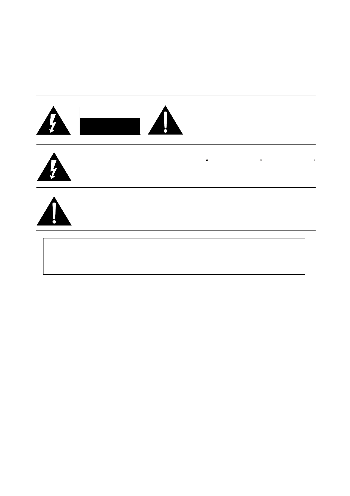
The lighting flash with arrowhead symbol, with an equilateral triangle is intended to
alert the user to the presence of uninsulated voltage within the products
enclosure that may be of sufficient magnitude to constitute a risk of electric shock to
the person.
The exclamation point within an equilateral triangle is intended to alert the user to the
presence of important operating and maintenance (servicing) instructions in the
literature accompanying the appliance.
DO NOT
C
OPEN.
ELECTR ICAL SHOCK , DO NOT RE MOVE
COVER (OR BACK). NO USER SERVICEABLE
PAR TS INS IDE . RE FE R SE R VIC ING TO
QUALIFIE D SERVIC E PERSONNEL.
dangerous
WARNING: TO REDUCE RISK OF FIRE OR ELECTRIC SHOCK, DO NOT
EXPOSE THIS APPLIANCE TO RAIN OR MOISTURE.
2
Page 3

SCHNEIDER ELECTRONICS GMBH-GERMANY
3
IMPORTANT SAFETY INSTRUCTIONS
CAUTION:
Read all of these instructions. Sa ve these instructions for later use . Follo w all W arnings and
Instructions marked on the audio equipment.
1. Read Instructions-All the safety and operatinginstructionsshouldbe read before the productis operated.
2. Retain Instructions- The safety and operating instructions should be retained for future reference.
3. Heed Warnings- All warnings on the product and in the operating instructions should be adhered to.
4. Follow Instructions- All operating and use instructions should be followed.
FOR YOUR PERSONAL SAFETY
1. When the power cord or plug is damaged or frayed, unplug this television set from the wall outlet and refer servicing to
qualified service personnel.
2. Do not overload wall outlets and extension cords as this can result in fire or electric shock.
3. Do not allow anything to rest on or roll over the power cord, and do not place the TV where power cord is subject to
traffic or abuse. This may result in a shock or fire hazard.
4. Do not attempt to service this television set yourself as opening or removing covers may expose you to dangerous
voltage or other hazards. Refer all servicing to qualified service personnel.
5. Never push objects of any kind into this television set through cabinet slots as they may touch dangerous voltage
points or short out parts that could result in a fire or electric shock. Never spill liquid of any kind on the television set.
6. If the television set has been dropped or the cabinet has been damaged, unplug this television set from the wall outlet
and refer servicing to qualified service personnel.
7. If liquid has been spilled into the television set, unplug this television set from the wall outlet and refer servicing to
qualified service personnel.
8. Do not subject your television set to impact of any kind. Be particularly careful not to damage the picture tube surface.
9. Unplug this television set from the wall outlet before cleaning. Do not use liquid cleaners or aerosol cleaners. Use a
damp cloth for cleaning.
10.1. Do not place this television set on an unstable cart, stand, or table. The television set may fall, causing serious injury
to a child or an adult, and serious damage to the appliance. Use only with a cart or stand recommended by the
manufacturer, or sold with the television set. Wall or shelf mounting should follow the manufacturer s instructions, and
should use a mounting kit approved by the manufacturer.
10.2. An appliance and cart combination should be moved with care. Quick stops, excessive force, and uneven surfaces
may cause the appliance and cart combination to overturn.
3
Page 4
SCHNEIDER ELECTRONICS GMBH-GERMANY
4
PROTECTION AND LOCATION OF YOUR SET
11. Do not use this television set near water ... for example, near a bathtub, washbowl, kitchen sink, or laundry tub, in a
wet basement, or near a swimming pool, etc.
Never expose the set to rain or water. If the set has been exposed to rain or water, unplug the set from the wall
outlet and refer servicing to qualified service personnel.
12. Choose a place where light (artificial or sunlight) does not shine directly on the screen.
13. Avoid dusty places, since piling up of dust inside TV chassis may cause failure of the set when high humidity persists.
14. The set has slots, or openings in the cabinet for ventilation purposes, to provide reliable operation of the receiver, to
protect it from overheating. These openings must not be blocked or covered.
Never cover the slots or openings with cloth or other material.
Never block the bottom ventilation slots of the set by placing it on a bed, sofa, rug, etc.
Never place the set near or over a radiator or heat register.
Never place the set in enclosure, unless proper ventilation is provided.
a built-in
PROTECTION AND LOCATION OF YOUR SET
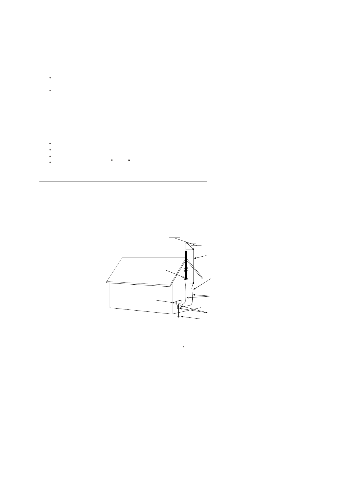
15.1. If an outside antenna is connected to the television set, be sure the antenna system is grounded so as to provide some
protection against voltage surges and built up static charges, Section 810 of the National Electrical Code, NFPA No.
70-1975, provides information with respect to proper grounding of the mast and supportingstructure, grounding of the
lead-in wire to an antenna discharge unit, size of grounding conductors, location of antenna discharge unit, c onnection
to grounding electrode, and requirements for the grounding electrode.
EXAMPLE OF ANTENNA GROUNDING AS PER NATIONAL ELECTRICAL CODE INSTRUCTIONS
EXAMPLE OF ANTENNA GROUNDING AS PER
NATIONAL ELECTRICALCODE
ANTENNA
LEAD- IN WIRE
GROUND CLAMP
ELECTRIC SERVICE
EQUIPMENT
NEC-NATIONAL ELECTRICALCODE
ANTENNA DISCHARGE
UNIT (NEC SECTION
810-20)
GROUNDING
CONDUCTORS
(NECSECTION 810-21)
GROUND CLAMPS
POWER SER VICE GROUNDING
ELECTRODE SYSTEM
(NEC ART 250. PART H)
15.2. Note to CATV system installer : (Only for the television set with CATV reception)
This reminder is provided to call the CATV system attention to Article 820-40 of the NEC that provides
installer s
guidelines for proper grounding and, in particular, specifies that the cable ground shall be connected to the grounding
system of the building, as close to the point of cable entry as practical.
16. An outside antenna system should not be located in the vicinity of overhead power lines or other electric lights or power
circuits, or where it can fall into such power lines or circuits. When installing an outside antenna system, extreme care
should be taken to keep from touching such power lines or circuits as contact with them might be fatal.
17. For added protection for this television set during a lightning storm, or when it is left unattended and unused for long
periods of time, unplug it from the wall outlet and disconnect the antenna. This will prevent damage due to lightning
and power-line surges.
4
Page 5

SCHNEIDER ELECTRONICS GMBH-GERMANY
5
OPERATION OF YOUR SET
18.
This television set should be operated only from the type of power source indicated on the marking label.If you are not
sure of the type of power supply at your home, consult your television dealer or local power company. For television
sets designed to operate from battery power, refer to the operating instructions.
19. If the television set does not operate normally by following the operating instructions, unplugthis television set from the
wall outlet and refer servicing to qualifiedservice personnel. Adjust only those controls that are covered in the operating
instructions as improper adjustment of other controls may result in damage and will often require extensive work by a
qualified technician to restore the television set to normal operation.
20. When going on a holiday : If your television set is to remain unused for a period of time, for instance, when you go on
a holiday, turn the television set and unplug the television set from the wall outlet.
off
IF THE SET DOES NOT OPERATE PROPERLY
21. If youare unable to restore normaloperationby followingthedetailedprocedurein your operating instructions,
do not attempt any further adjustment. Unplug the set and call your dealer or service technician.
22. Whenever the television set is damaged or fails, or a distinct change in performance indicates a need for
service, unplug the set and have it checked by a professional service technician.
23. It is normal for some TV sets to make occasional snapping or popping sounds, particularly when being
turned on or off. If the snapping or popping is continuous or frequent, unplug the set and consult your
dealer or service technician.
FOR SERVICE AND MODIFICATION
24. Do not use attachments not recommendedby the television set manufacturer as they may cause hazards.
25. When replacementparts are required,be sure the service technician has used replacementparts specified
by the manufacturer that have the same characteristics as the original part. Unauthorized substitutions
may result in fire, electric shock, or other hazards.
26. Upon completion of any service or repairs to the television set, ask the ser vice technician to perform
routine safety checks to determine that the television is in safe operating condition.
5
Page 6
2. SPECIFICATION
6
Environment
Screen Parameter
Color System
TV:■PAL – DK ■PAL – I ■NTSC-M ■PAL – BG □PAL – N □PAL – M □SECAM □SECAM-L □Other:
AV:■NTSC4.43 ■NTSC3.58 ■PAL ■SECAM □Other:
Nicam
■NICAM □MTS □FM-FM □German Stereo □BTSC □SAP □Other:
Program
□Program Auto Mark □Program Compositor ■Auto Searching ■Manual Searching ■Tuning □Other:
Teletext Type: Pages:
□CCD □V-CHIP □Macro Vision □HDCP
Audio:
□Insert SPK. ■Insert Amplifier ■Sound Effect ■AVC □Output Power(W): 1.5W*2
□SRS □EQ: Steps:
■Sound Effect Adjustment: ■Bass ■Treble □Balance □Others:
Antenna Input: □BNC ■IEC □Other:
Operation Temperature( ):℃ 0~50
Operation Humidity(%): 20%~90%RH(0~40℃) Store Humidity(%): 20%~90%RH(-20~40℃)
Air Pressure(kps)
Screen Size(inch):20.1
Effective Size(mm x mm):
mm(H) X 306mm(V)
408
Angle of View (H/V): □160/160 ■160/140 □Other:
Responsive Time (ms):
■8 □12 □16 □25 □Other:
Contrast ( Darkness, Nakedness): 600
Background Light:6-CCFL Backlight unit
Colors:Supporting 16.7 M
Gray:256
Max. V. Frequency(Hz): 70Hz
Resolution: ■640×480 □852×480 □1024×768 □1280×720 □1280×768
□1280×1024 □1366×768 □1920×1080 □Other:
Max. Resolution(H×V): □640×480 □800×600 ■1024×768 □1400×1050
□1600×1200 □1280×800 □1280×854 □1920×1200 □Other:
HDTV/SDTV(p): ■1920×1080i □1920×1080p □1920×1125i □1440×1080i
■1280×720P ■576P ■720×480p □Other:
:
Store Temperature( ):℃ -20~60
Panel size(mm x mm x mm):
448.6mm(H) X 339.6mm(V) X 23.6 (D)
Panel Type:TFT LCD
Image Size(mm x mm):
0.2125(H) x 0.6375(V)
Luminance of Peak Value(cd/m²):500
Ratio: □16:9 ■4:3 □Other:
Color Temperature(°K):
Cool: 11000, Standard: 9300, Warm:7000
Max. H. Frequency(KHz): 56.5kHz
Input
Video
Audio
■VGA Input (Type:D-15 Quantity: 1 )
■Component ( ■RCA □ BNC □SCART □Other: )
■Composite ( ■RCA □BNC □SCART □Other: )
□ DVI Input (Type: Quantity: )
□ HDMI Input (Type: Quantity: )
□RGB Input (□ SCART □ Other: )
■S-Video Input (Quantity: 1 )
■Audio Input(RCA) (Quantity : 1 )
■Earphone Input (Quantity : 1 )
Page 7
7
Output
OSD:
Languages: □Chinese ■English ■Russian □Other:
Adjustment via OSD:
■Contrast ■Chroma ■H/V - size(YCbCr) □Picture Rotation ■Brightness ■Tint ■H/V - position(YCbCr) □Other:
Certification
□CCC □CE □UL □CUL □FCC □FDA ■CB □RoHS □Other
Power Supply:
Max. Power Consumption(W): 55W Voltage(V): 110-240V~
Standby Power Consumption(W):< 6W ■Switch on/off ■Auto stand-by (Timer:5 Min.) ■Other:Time On
Accessories:
■Remote Control ■Stand (Optional) □Scart Cord ( m) □Bracket(Optional) □Bracket Accessories(Optional)
■Power Supply Cord □Antenna (1.8 m) □Speakers (Optional) □VGA line (Type: ) ■Other:Adapter
Video
Audio
□Composite Video (□RCA □BNC □SCART □Other: )
□Audio Output (L/R) (□RCA)
□Audio Output 5.1
□Speaker (Insert Amplifier)
□Audio Digital Coaxial (RCA)
□Audio digital optical
■Earphone Output
Packing
Unit Size(w×h×d, mm): 609X500X79 NET(kg): 11
Packing Size(w×h×d, mm): 700X590X290 Gross Weight(kg): 15.5
Page 8

3.Bom List
8
ITEM SPEC. QTY LOCATION
T6-0Q0036-H027X REMOTE HANDSET ASSEMBLY 1
11-0BC337-0BX TRANSISTOR (NPN) BC337-40 1 Q1
13-00AS12-13B IC AS1213B 1 U1
14-IRE05B-XX0 IR EMITTING DIODE TSAL6200 1 D2
18-CB0221-JNX RES. C.F. 220 OHM 1/6W +/-5% 1 R2
18-CB0229-JNX RES. C.F. 2.2 OHM 1/6W +/-5% 1 R1
25-HBB479-M1X CAP. ELEC 4.7 UF 10V +/-20% 1 C4
26-EBP101-JCS CAP. CER 100 PF 50V +/-5% 2 C2;C1
26-EBP103-ZFX CAP. CER 0.01UF 50V +80/-20% F 1 C3
40-LD40V8-RMC1X P.C.B.REMOTE HANDSET BD 1
41-WJ0050-B00 WIRE BARE JUMPER 5MM 1 J1
45-COS455-KY0 CERAMIC RESONATOR 455KHZ 1 Y1
67-X38064-0E2 BATTERY SPRING (+/-) 1
67-X38065-0E2 BATTERY SPRING (+) 1
67-X38066-0E2 BATTERY SPRING (-) 1
71-270870-0A9 LABEL 1
74-007026-60C POLYBAG (70MMX260MMX0.06MM) 1
T6-0Q0036-H027XZ REMOTE HANDSET ASSEMBLY 1
49-HS36Q0-00X1E RUBBER PAD KEYS 1
55-HS36QB-0HA1A QREMOTEHANDSET-BOTTOMCABINET 1
55-HS36QD-0HA1A QBATTDOOR-REMOTEHANDSET 1
55-HS36QT-0HA1H TOP CASE 1
56-399030-0HC5Z REMOTE HANDSET LENS 1
58-HS36Q0-FUI1A INLAY REMOTE HANDSET 1
T8-JV6TRT-BSY ASS'Y - BASE 1
59-100010-000 FOOT CUSHION 8
63-B30080-BT3 SCREW BT BID 3 X 8 STL BZN 10 MTG BASE COVER-SEEEL-PLATE
63-B30120-AB2 S/T SCREW B 3 X 12 AB 2 MTG BASE FRONT CAB & BASE REAR CAB
64-F40080-103 M/C SCREW F 4 X 8 9 MTG HINGE-ASSEM & SEEEL PLATE
67-M80437-0E0 SOLEPLATE 1
68-804360-000 HINGE-ASSEMBLY 1
T8-JV6TRT-BSYZ ARFBASE ASSEMBLY 1
55-803720-0HA1B BASE COVER 1
55-803740-0HA6L FRONT PANEL 1
55-803750-0HA6L REAR PANEL 1
T8-JV6TRT-FBY FRONT CONTROL BD ASSEMBLY 1
40-LD20V6-FBD1X P.C.B.FRONT CTL BD 1
46-35199W-03X PIN BASE *3 PITCH=2.0MM 1 J001
46-35199W-05X CONN.PH-5A 5PIN PITCH=2.0MM 1 J1001
46-39699H-03X 3P UL2547#24 610MM 1 FRONT CTL BD TO DIGITAL (J11)
46-39737H-05X UL20080#28 510MM 1 J1001 TO DIGITAL (J7)
48-POW001-XX0 SWITCH POWER KDC-A11 B2 1 SW001
48-TAC002-XX0 TACT SWITCH 6
57-LEDH05-000 LED BRACKET 1 FOR IR01
SW1006;SW1005;SW1004;SW1003;SW1002;
SW1001
Page 9

ITEM SPEC. QTY LOCATION
9
02-IRR001-XX1 IR RECEIVER MODULE HRM380017 1 IR01
11-SC1815-YBX TRANSISTOR 2SC1815-Y (NPN) 1 Q1001
14-LED03R-XX1 LED RED Φ3MM FO203 1 LED1001
18-CB0100-JNX RES. C.F. 10 OHM 1/6W +/-5% 1 R1008
18-CB0103-JNX RES. C.F. 10K OHM 1/6W +/-5% 1 R1006
18-CB0122-JNX RES. C.F. 1.2K OHM 1/6W +/-5% 1 R1005
18-CB0182-JNX RES. C.F. 1.8K OHM 1/6W +/-5% 1 R1004
18-CB0272-JNX RES. C.F. 2.7K OHM 1/6W +/-5% 1 R1003
18-CB0332-JNX RES. C.F. 3.3K OHM 1/6W +/-5% 1 R1002
18-CB0102-JNX RES. C.F. 1K OHM 1/6W +/-5% 1 R1007
18-CB0562-JNX RES. C.F. 5.6K OHM 1/6W +/-5% 1 R1001
25-HCB100-M1X CAP. ELEC 10 UF 16V +/-20% 1 C1002
T8-JV6TRT-FCN FRONT CABINET ASSEMBLY 1
42-51208D-XX3 SPEAKER YDA512-6C 8 OHM 5W 2
4A-LCD20T-CM2 20"CMO TFTSCREEN V201V1-T03 1
81-BLI006-XX4 INVERTER 1
T8-JV6TRT-FCNZ ASS'Y-ARFFRONTCABINET 1
55-803700-0UA1B FRONT CABINET 1
56-707220-0HA4R POWER KNOB 1
56-804690-0HA4R PUSH BUTTON 1
57-804860-0HC1B DECORATE BAR 1
T8-JV6TRT-PAN PACKING ASSEMBLY 1
49-204260-BAT 7# BATT. UM4 R03P SIZE AAA 2
51-PC0220-0ZU08 POWER CORD 1
54-LCPVC1-001 PROTECT INLAY 1
81-ADT125-201 ADAPTER SAWA-02-520 1
T8-JV6TRT-PANZ ASS'Y-ARFPACKINGPARTS 1
T8-JV6TRT-RCN REAR CABINET ASSEMBLY 1
63-B30120-AB3 S/T SCREW B 3.0 X 12 4 MTG REAR CAB -FRONT CAB
64-F40080-103 M/C SCREW F 4 X 8 6 MIG REAR CAB & HINGE- ASSEMBLY
T8-JV6TRT-RCNZ ASS'Y-ARFREARCABINET 1
55-718300-0HA1A COVER BOARD(LEFT) 1
55-718310-0HA1A RIGHT COVER 1
55-803710-0UA1B REAR CABINET 1
55-803730-0HA1B BASE SUPPORT COVER(LEFT) 1
55-804790-0HA1B BASE SUPPORT COVER(RIGHT) 1
58-20B6MP-0UI1A PLATE MODEL NO. 1
58-805930-0UI1B INLAY(LEFT) 1
58-805940-0UI1B INLAY(RIGHT) 1
T8-JV8AXT-DIY DIGITAL BD ASSEMBLY 1
09-0BAV99-ATX HIGH SPEED DOUBLE DIODE BAV99 6 D8;D7;D6;D4;D1;D3
09-BAV70L-ATX SMD. DIODE BAV70LT1(SOT-23) 215 2 D5;D2
09-FM4001-ETX SMD.DIODE FM4001 2 D12;D11
09-LL4148-ATX SMD. SWITCHING DIODE LL4148 1 D10
10-1N5820-F0X DIODE 1N5820 1 D9
12-BC847C-0BX SMD.TRANSISTOR BC847C 7 Q6;Q5;Q4;Q3;Q2;Q10;Q1
12-BC848B-0BX TRANSISTOR BC848B 1 Q11
Page 10

ITEM SPEC. QTY LOCATION
10
12-BT3904-0BX SMD. TRANSISTOR MMBT3904LT1(NPN) 3 Q8;Q9;Q7
13-024LC1-6BB IC 24LC16B 1 U7
13-1117MP-18B IC LM1117MPX-1.8 2 U14;U13
13-39SF02-0AB IC 39SF020A-PLCC32 (WRITE) 1 U6
13-AT24C0-20B IC AT24C02 SO-8 EEPROM 2K BIF(WRITE) 1 U2
13-GM2221-00B SCALER IC GM2221 1 U4
13-IC1084-CMB IC AIC1084-33CM 3.3V (TO-263) 1 U10
12-30PF03-0BX TRANSFORMER STD30PF03LT4 1 U11
13-LD1117-33B IC LD1117 3.3V 1 U12
13-MIC457-6UB IC MIC4576-5.0 1 U9
13-PI5V33-0QB IC PI5V330Q (QSOP) 1 U3
13-SI9953-DYB IC SI9953DY(8-PIN) 1 U8
13-SN74HC-14B IC SN74HC14D-SOP14 1 U5
13-TVP514-7PB IC TVP5147PFP 1 U15
19-AB0000-JTX RES SMD 0 OHM 1/10W +/-5% 0603 7 0R3;R107;R13;R85;0R2;R10;R11
19-AB0101-JTX RES SMD 100 OHM 1/10W 0603 16
19-AB0102-JTX RES SMD 1K OHM 1/10W 0603 10
19-AB0103-JTX RES SMD 10K OHM 1/10W 0603 24
19-AB0104-JTX SMD. RES 100K OHM 1/10W 0603 1 R101
19-AB0121-JTX SMD. RES 120 OHM 1/10 J 0603 5 R110;R112;R108;R105;R103
19-AB0152-JTX SMD. RES 1.5K OHM 1/10W +/-5% 0603 1 R128
19-AB0202-JTX SMD. RES 2K OHM 1/10W +/-5% 0603 1 R79
19-AB0220-JTX SMD RES 22 OHM 1/10W 0603 9 R7;R5;R93;R92;R94;R95;R137;R23;R27
19-AB0222-JTX RES SMD 2.2K OHM 1/10W 0603 7 R133;R134;R126;R125;R123;R131;R132
19-AB0223-JTX SMD. RES 22K OHM 1/10W +/-5% 0603 7 R47;R46;R42;R41;R26;R24;R136
19-AB0271-JTX SMD. RES 270 OHM 1/10W +/-5% 0603 1 R53
19-AB0272-JTX RES SMD 2.7K OHM 1/10W 0603 1 R16
19-AB0333-JTX RES. SMD 33K OHM 1/10W 0603 1 R139
19-AB0470-FTX RES SMD 47 OHM 1/10W +/-1% 0603 3 R28;R25;R22
19-AB0471-JTX SMD. RES 470 OHM 1/10W +/-5% 2 R80;R119
19-AB0472-JTX RES SMD 4.7K OHM 1/10W 0603 5 R83;R91;R64;R76;R77
19-AB0473-JTX SMD. RES 47K OHM 1/10W 0603 2 R89;R15
19-AB0682-JTX RES SMD 6.8K OHM 1/10W 0603 1 R130
19-AB0820-JTX SMD. RES 82 0HM 1/10W +/-5% 0603 14
19-BB0101-JTX SMD. RES 100 OHM 1/10W +/-5% 1 R96
19-BB0103-JTX SMD. RES 10K OHM 1/10W +/-5% 1 R97
19-BB0222-JTX SMD. RES 2.2K OHM 1/10W +/-5% 1 R98
19-CC0000-JTX CHIP RESISTOR 1 R87
23-A08220-JBX NETWORK RES. 22 OHM +/-5% 6 RN4;RN2;RN1;RN3;RN6;RN5
23-A08470-JBX CHIP ARRAY RES. 47 OHM +/-5% 0603*4 2 RN7;RN8
25-BCB331-M1X CAP. ELEC 330 UF 16V +/-20% 3 C83;C86;C82
25-BCL100-M1X CAP.ELEC 10UF 16V +/-20% 2MM 7 C11;C13;C14;C4;C17;C16;C15
25-BCL101-M1X CAP.ELEC 100UF 16V +/-20% 15
R121;R122;R124;R127;R129;R17;R18;R4; R6
;R99;R143;R118;R120;R117;R116;R100
0R4;0R1;R90;R84;R82;R37;R34;R29;R140;
R138
R33;R31;R30;R68;R59;R56;R52;R51;R50;R35;R
48;R45;R43;R9;R8;R78;R75;R74;R1;R102;
R115;R12;R135;R14
R111;R49;R40;R39;R104;R106;R109;R113;
R19;R20;R38;R36;R32;R21
C104;C105;C110;C111;C114;C115;C125;C78;C
85;C94;C95;C97;C99;C230;C232
Page 11

ITEM SPEC. QTY LOCATION
11
25-BCL220-M1X CAP. ELEC 22 UF 16V +/-20% (5X11) 8 C48;C73;C75;C38;C29;C18;C108;C102
25-BDA471-M1X CAP. ELEC 470 UF 25V +/-20% 2 C91;C79
28-AB0100-JCX SMD. CAP 10 PF 50VDC +/-5% 1 C143
28-AB0102-ZFX CAP.SMD 1NF 50V +80-20% 0603 1 C3
28-AB0103-ZFX CAP.SMD 10NF 50V +80-20% 0603 7 C7;C6;C8;C9;C5;C12;C10
C19;C34;C33;C32;C31;C30;C28;C27;C26;
C25;C160;C159;C155;C153;C152;C151;C150;
C139;C2;C161;C162;C163;C165;C167;C168;
C173; C134;C133;C124;C122;C121;C116; C113;
C112;C109;C107;C106;C103;C101;C24;
28-AB0104-ZFX CAP. SMD 0.1UF 50V +80%~-20% F 90
28-AB0150-JCX CAP.SMD 15P 50V +/-5% 0603 2 C171;C169
28-AB0221-JCX CAP.SMD 220PF 50V C 0603 +/-5% 5 C55;C64;C66;C46;C47
28-AB0222-KBX CAP.SMD 2200PF 50V +/-10% 0603 6 C190;C184;C180;C177;C176;C175
28-AB0330-JCX SMD CAP 33PF 50V +/-5% 2 C118;C117
28-AB0331-JCX SMD. CAP 330 PF 50V +/-5% 0603 14
28-AB0470-JCX CAP.SMD 47PF 50V +/-5% 0603 1 C76
28-AB0479-CCX SMD. CAP 4.7 PF 50V +/-0.25PF 5 C119;C126;C157;C147;C140
28-AB0509-CCX CAP.SMD 5PF 50V +/-0.25PF 2 C58;C59
28-AB0561-JCX SMD. CAP 560 PF 50VDC +/-5% 0603 1 C166
28-AB0682-KBX SMD. CAP 6800PF 50VDC +/-10% 1 C172
28-AB0683-ZFX SMD CAP. 68NF 50V +80/-20% 0603 1 C174
28-AB0809-CCX CAP.SMD 8PF 50V +/-0.25PF 1 C63
28-BB0101-JCX SMD CAP. 100 PF 50V C 0805 1 C89
28-BB0104-ZFX SMD CAP. 0.1 UF 50V +80/-20% 0805 10
33-ELL339-KTX SMD. COIL 3.3 UH +/-10% 0805 5 L46;L47;L49;L51;L50
33-GLN100-NTX CHIP BEAD 10 OHM +/-25% 3 FB2;FB3;FB1
33-GLN300-NTX CHIP BEAD 30 OHM +/-25% 38
33-KLL279-KTX SMD. COIL 2.7UH +/-10% 0603 5 L37;L36;L35;L34;L30
33-KLN121-NTX CHIP BEAD 120 OHM +/-25% 1 R114
36-LIF020-XX0 LINE FILTER LC-33-TCL 1 L15
40-20V8AT-DIB4X P.C.B DIGIBOARD 1
43-SFSS11-2DM RELAY SF-SS-112DM 1 RELA1
45-OSC14M-3Y2 CRYSTAL 14.31818MHZ 2 X2;X1
46-33079W-04X PIN BASE *4 TJC3-4A 1 J1
46-35199W-02X CONN. PH-2A PITCH=2.0MM 2 T2;J11
46-35199W-05X CONN.PH-5A 5PIN PITCH=2.0MM 1 J7
46-35199W-07X CONN.PH-7A PITCH=2.0MM 7PIN 1 J9
46-39555W-50X CONNECTION(FFC FPC) 1 J2
46-39707H-15X 15P UL20080#28 60MM 1
C23;C223; C220;C22;C21;C20;C138;C100;
C137;C136; C135;C35;C36;C37;C39;C40;C41;
C42; C43; C44;C45;C49;C50;C51;C52;C53;
C54;C93; C57;C60;C61;C62;C65;C67;C68;
C69;C70; C71;C72;C74;C80;C81;C84;C87;
C56;C225; C98;C96;C231;C233
C120;C127;C141;C142;C148;C149;C229;C228;
C164;C158;C156;C224;C226;C227
C92;C90;C88;C77;C154;C146;C145;C144;
C130;C128
L32;L31;L25;L13;L33;L38;L4;L40;L41;L12;L26;
L9;L8;L7;L6;L5;L27;L28;L29;L3;L18;L19;L14;
L16;L17;L2;L1;F1;L20;L21;L22;L23;L24;L11;
L10;L39;L48;L52
J3、J5
Page 12

ITEM SPEC. QTY LOCATION
12
46-40001H-50X HS 50PIN PSK0500035A-006222 VER 0 1
46-FF045F-07B 6P UL1007#26 450MM 1
46-FH006F-10P01 UL20080#28 PH-10Y/JC20-5Y+JC25-5Y 1
47-PWS012-XX0 SOCKET DSW-47 1 JP1
47-RCA125-XX1 RCA SOCKET AV-3.2-3W-051 1 P1
47-VGA002-XX0 VGA JACKET D-SUB-15WP 1 CN2
64-B30080-104 M/C SCREW B 3 X 8 1 FOR U11
65-Z30050-23M NUT M 3 1 FOR U11
67-387190-0A0 HEAT SINK 1 FOR U4
71-268390-0A0AF LABEL (QC) GREEN 1
71-AV0000-T02 BARCODE LABEL 1
13-L7809C-D2B IC L7809CD2T-TR (DDPAK) 1 U11B
13-L7805C-2TB IC L7805CD2T (REGULATOR) 1 U11C
V8-LM21V6-01D01 SOFTWARE CODE 1 FOR U2
V8-LM21V6-01F01 SOFTWARE CODE 1 FOR U6
T8-JV8AXT-ANY CONGRAGATE BD ASSEMBLY 1
07-380FI5-TB0G TUNER TMQZ6-429B 1 TU701
09-LL4148-ATX SMD. SWITCHING DIODE LL4148 4 D701;D501;D505;D504
12-BC847A-0BX SMD TRANSISTOR BC847A (NPN) 4 Q707;Q704;Q706;Q705
12-BT3904-0BX SMD. TRANSISTOR MMBT3904LT1(NPN) 4 Q508;Q702;Q501;Q701
13-MC3406-3AB IC MC34063AD (SO-8) 1 U701
13-MSP341-0TB IC MSP3410G(64PINS) 1 IC502
13-TPA151-7NP IC TPA1517NE 1 IC503
19-AB0000-JTX RES SMD 0 OHM 1/10W +/-5% 0603 6 R527;R706;R539;R535;R534;R538
19-CC0000-JTX CHIP RESISTOR 2 D502;R525
19-AB0273-JTX SMD. RES 27K OHM 1/10W +/-5% 2 R528;R547
19-AB0101-JTX RES SMD 100 OHM 1/10W 0603 9
19-AB0102-FTX RES SMD 1K OHM 1/10W +/-1% 0603 1 R748
19-AB0102-JTX RES SMD 1K OHM 1/10W 0603 10
19-AB0103-JTX RES SMD 10K OHM 1/10W 0603 9
19-AB0104-JTX SMD. RES 100K OHM 1/10W 0603 5 R713;R717;R738;R739;R526
19-AB0109-JTX RES SMD 1 OHM 1/10W +/-5% 1 R504
19-AB0181-JTX SMD. RES 180 OHM 1/10W 0603 1 R707
19-AB0184-JTX RES SMD 180K OHM 1/10W +/-5% 0603 1 R779
19-AB0221-JTX RES SMD 220 OHM 1/10W 0603 2 R744;R501
19-AB0223-JTX SMD. RES 22K OHM 1/10W +/-5% 0603 6 R724;R723;R722;R704;R701;R502
19-AB0229-JTX SMD. RES 2.2 OHM 1/10W J 0603 1 R746
19-AB0243-FTX 0603 RES. SMD 24K OHM 1/16W +/-1% 1 R747
19-AB0331-JTX RES. SMD 330 OHM 1/10W 0603 3 R505;R703;R709
19-AB0332-JTX SMD RES 3.3K OHM 1/10W 0603 2 R710;R715
19-AB0471-JTX SMD. RES 470 OHM 1/10W +/-5% 1 R705
19-AB0473-JTX SMD. RES 47K OHM 1/10W 0603 1 R719
19-AB0682-JTX RES SMD 6.8K OHM 1/10W 0603 2 R712;R716
19-AB0683-JTX RES SMD 68K OHM 1/10W 0603 1 R708
19-AB0820-JTX SMD. RES 82 0HM 1/10W +/-5% 0603 3 R742;R743;R736
J4、J8
R515;R507;R530;R516;R508;R740;R714;R711;
R506
R512;R514;R509;R729;R727;R734;R735;R737;
R741;R752
R731;R732;R733;R728;R730;R503;R510;R533;
R532
Page 13

ITEM SPEC. QTY LOCATION
13
25-BCB100-M1X CAP. ELEC 10 UF 16V +/-20% 3 C701;C724;C560
25-BCB471-M1X CAP. ELEC 470 UF 16V +/-20% 3 C542;C704;C703
25-BDB221-M1X CAP. ELEC 220UF 25V +/-20% 2 C549;C548
25-BDB470-M1X CAP. ELEC 47 UF 25V +/-20% 5 C528;C522;C527;C530;C513
25-BFB100-M1X CAP. ELEC 10 UF 50V +/-20% 6 C537;C524;C550;C551;C536;C511
25-BFB220-M1X CAP. ELEC 22 UF 50V +/-20% 1 C726
25-BFB229-M1X CAP. ELEC 2.2 UF 50V +/-20% 1 C541
25-BFB339-M1X CAP. ELEC 3.3 UF 50V +/-20% 1 C533
25-BFB470-M1X CAP. ELEC 47 UF 50V +/-20% 2 C546;C720
25-HCB220-M1X CAP. ELEC 22 UF 16V +/-20% 7 C717;C716;C714;C710;C709;C719;C718
28-AB0102-KBX SMD. CAP 1000 PF 50V +/-10% B 7 C552;C553;C556;C557;C526;C538;C525
28-AB0103-ZFX CAP.SMD 10NF 50V +80-20% 0603 8 C512;C721;C509;C521;C702;C705;C523;C516
28-AB0104-ZFX CAP. SMD 0.1UF 50V +80%~-20% F 5 C715;C510;C540;C532;C544
28-AB0151-JCX SMD. CAP 150 PF 50V +/-5% C 1 C723
28-AB0152-KBX SMD. CAP 1500 PF 50V +/-10% B 1 C531
28-AB0222-KBX CAP.SMD 2200PF 50V +/-10% 0603 1 C543
28-AB0224-ZFX CAP.SMD 0.22UF 50V +80-20%0603 4 C722;C725;C727;C707
28-AB0339-CCX SMD.CAP. 50V 3.3PF +/-0.25PF 2 C518;C519
28-AB0470-JCX CAP.SMD 47PF 50V +/-5% 0603 2 C508;C507
28-AB0471-JCX CAP.SMD 470PF 50V +/-5% 0603 4 C501;C502;C529;C503
28-AB0560-JCX SMD CAP. 56 PF 50V +/-5% 0603 2 C515;C517
28-DC0107-MTX TANTALUM CAP. 100 UF 16VDC +/-20% 1 C706
28-XC0106-MTX TANTALUM CAP.10 UF 16V +/-20% 1 C713
33-KLN102-NTX SMD.COLL MGGB1608M102HB 2 L704;L702
34-R101J2-0EX COIL PL - 100 UH +/-5% 3 L505;L504;L703
34-R120J2-0EX COIL PL - 12 UH +/-5% 3 L506;L503;L701
34-R221J2-0EX COIL PL - 220 UH +/-5% 1 LN701
45-OSC18M-4Y0 CRYSTAL 18.432M 1 X501
46-30627H-02X HS 2P24 360/7 F/W TJC3-2Y 1 J704 TO SPEAKER(L)
46-33079W-02X PIN BASE *2 TJC3-2A 1 J704
46-35199W-02X CONN. PH-2A PITCH=2.0MM 1 J703
46-35199W-10X CONN. PH-10 10PIN PITCH=2.0MM 1 J707
46-35199W-15X CONN. PH-15A PITCH=2.0MM 1 J706
46-FT050T-02H CONNECTION 1 J703 TO SPEAKER(R)
47-EAR002-XX0 EARPHONE SOCKET CK3-3.5-9WK-B 2 JP702;JP701
47-RCA009-XX4 RCA SOCKET AV-3.2-3W-052 1 AV701
47-SVI008-XX1 SOCKET DSW-506WT-L 1 SZ701
71-268390-0A0AF LABEL (QC) GREEN 1
71-270870-0A9 LABEL 2
40-20V8AT-AMC2X P.C.B AM BD 1
Page 14

14
4. ALIGNMENT PROCEDURE
Flowchart of alignment procedure
To enter the Factory Mode
1. Press MENU button to enter the main menu, and press the password “3210” continuously to
enter the Factory Mode.
2. Press
3. Press MENU button to quit the Factory Mode.
Note: Set the FACTORY MODE to 1 in Advanced Setting of factory menu, then after exiting the
menu, press “OK” button to enter the factory mode directly without pressing password. Exit the
menu by pressing MENU button.
button to set FACTORY MODE to 0.
1. Adjustment
in VGA mode
2, 3. Adjustment of
White Balance
▼/▲ to select item, press ◀/▶ button to adjust the value.
But it must be set to 0
before delivery: Select the Init Value item, then press ▶
4. Check the
setting in the
Factory mode
ALIGNMENT PROCEDURE
1. Adjustment in VGA mode:
1) Required equipment: 2225 Signal Generator.
2) Connect the power adapter and generator, and press POWER button to switch the unit
on.
3) Press “PC Input” button to switch to VGA mode.
4) Input
5) Make sure the color is OK in these modes: 640×400 (60Hz) , 720×400 (60Hz), 640×480
1024 x 768 @ 60 Hz, Chessboard pattern signal. Enter Color Setting in Factory
Mode, and select Auto Adjust. to calibrate ADC to standard state.
(60Hz), 800×600 (60Hz),
1024X768(60HZ).
2. Auto adjustment of White Balance:
1) Auto adjustment in VGA /HDTV mode:
Required equipment:
A. Input 720p, Full White signal from
B. Switch to HDTV mode, and press PRESETS button to set the picture mode to
standard.
Confirm the baud rate of the Colour analyser is 9600(unlock the lock key—red led on is
C.
locked, and select the RS-232 key, the row 1 in the display screen will display the baud rate, you can
press the number key to change the value.). After setting, press the lock key to lock the baud rate.
D. Enter the Factory Mode
Select cool or standard or warm. Then enter the sub menu to select Y item, and
measure Y with the colour analyser and adjust it to a needed value (about
250 cd/㎡
). Then select AUTO item, and activate the auto adjustment.
Color analyzer Chroma7120, Specific series port interface
HDTV signal generator.
.
Chroma7120.
100cd/㎡ in VGA mode,
Page 15

15
2) Auto adjustment in TV/AV mode:
A. Switch to AV mode.
B. Input the Gray Scales signal.
C. Set the picture mode to Standard.
D. Enter the Basic Setting of Factory Mode to adjust Blacklight until the second dark
scale is just visible.
E. Change the input signal to H/2 White Reference signal and enter the Factory Mode.
Set Y to
250 cd/㎡, the method is same to that in VGA/HDTV mode.
3. Manual adjustment of white balance
1) VGA/HDTV mode
A. Select HDTV mode, then press PRESETS key in remote control to select Standard
picture mode.
Input H/2 White Reference signal, then adjust white balance.
B.
a. Cool color temperature: select cool in factory menu, and revise R, G, B gain value until
x=276±15, y=286±15.
b. Standard color temperature: select standard in factory menu, and revise R, G, B gain
value until x=284±15, y=299±15
c. Warm color temperature: select warm in factory menu, and revise R, G, B gain value
until x=305±15, y=320±15.
2) AV/TV mode
A. Select AV mode, then press PRESETS button to select Standard picture mode.
B. Input the Gray Scales signal and adjust Blacklight in factory menu until the second
dark scale is just visible.
C. Input
The method is same as above.
H/2 White Reference signal, then adjust white balance.
Note: If the EEPROM is fire-new, the values are set to default after powering on. In normal
condition, it needs just a little adjustment on the base of default values.
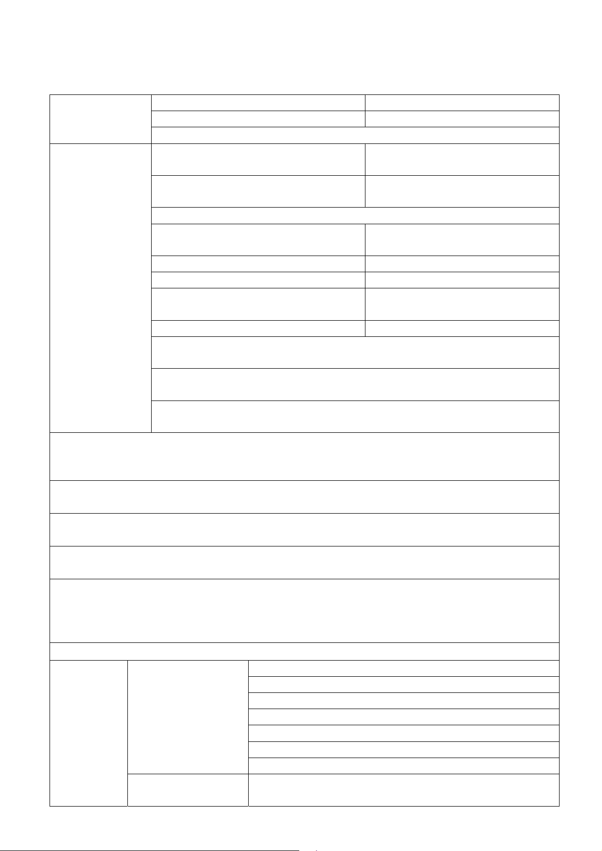
4. Check the setting in the Factory mode:
1) Basic Setting:
Item Default Description
Backlight ** Back light
Blacklight ** Sub brightness
NVRAM Addr ** NVRAM’s address
NVRAM VAL ** NVRAM’s value
Note: Adjustment of NVRAM is done only under the necessity.
2) Color Setting:
Item Default Description
Auto Adjust Auto adjusting ADC in PC mode
RED ** Manually adjusting ADC in PC mode.
GREEN ** Manually adjusting ADC in PC mode.
Page 16
16
BLUE ** Manually adjusting ADC in PC mode.
RED OFFSET ** Manually adjusting ADC in PC mode.
GREEN OFFSET ** Manually adjusting ADC in PC mode.
BLUE OFFSET ** Manually adjusting ADC in PC mode.
Note: If the White Balance is adjusted automatically, the manual adjustment will
not be available.
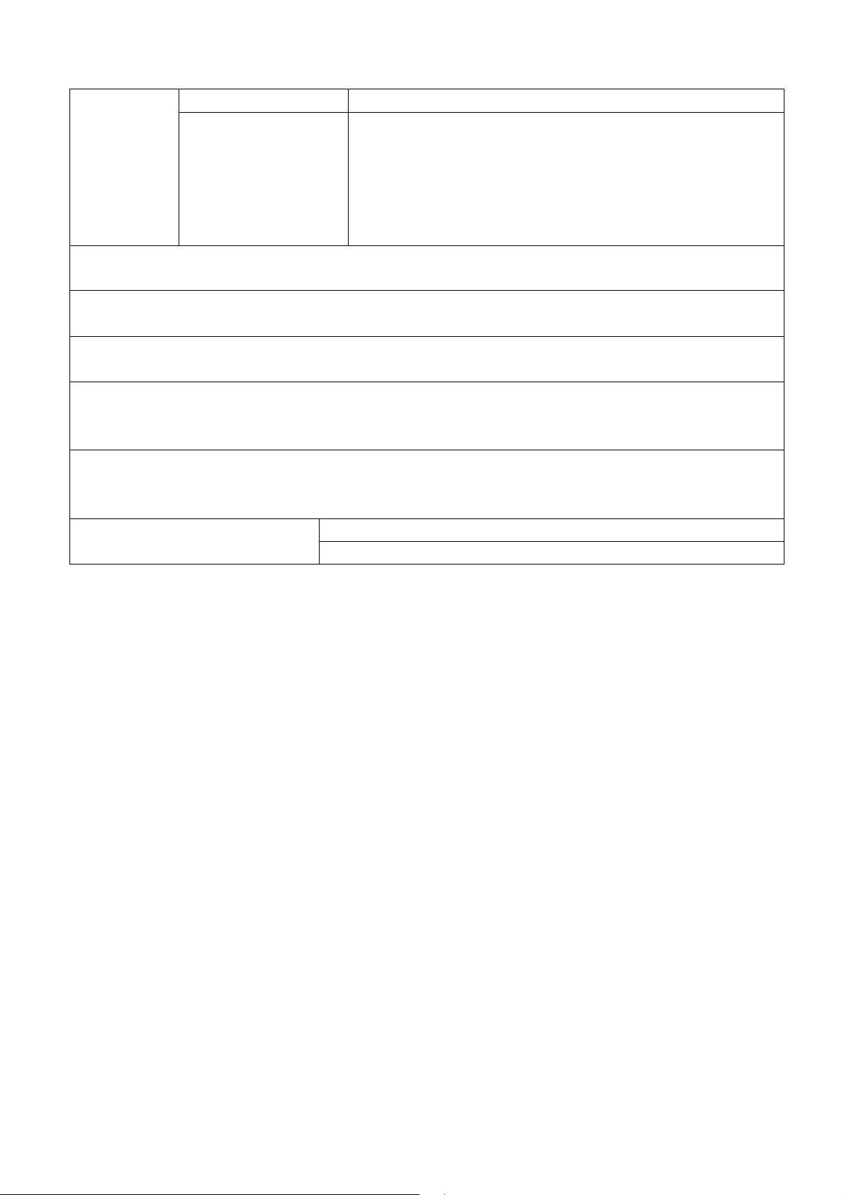
3) Sound Setting:
Item Default Description
Min Volume 0 Minimum Volume
Max Volume 100 Maximum Volume
Dot1 ** Volume value
Dot2 ** Volume value
Dot3 ** Volume value
Dot4 ** Volume value
4) 4200K/5000K/WARM/STANDARD/COOL/CUSTOM:
Only WARM, STANDARD and COOL need to be adjusted in White Balance adjustment.
Item Default Description
Brightness 50 Brightness
Contrast 50 Contrast
RED ** Red Gain
GREEN ** Green Gain
BLUE ** Blue Gain
Y ** The brightness of auto adj.
AUTO Auto adjustment
5) Advanced Setting:
Item Default Description
Factory Mode 0
Power Mode 1 To set the state of the unit after powered on.
Panel index 20 Panel index
Decoder SatHue 0 Decoder adjustment
Enable Zoom 0 To switch Zoom function on or off
Enable AVIPort 0 Enable or disable AVI Port
Enable DVIPort 0 Enable or disable DVI Port
Factory Reset Reset in Factory Mode
Set Init Value Reset before delivery
To set the method of entering the Factory
Mode.
Page 17
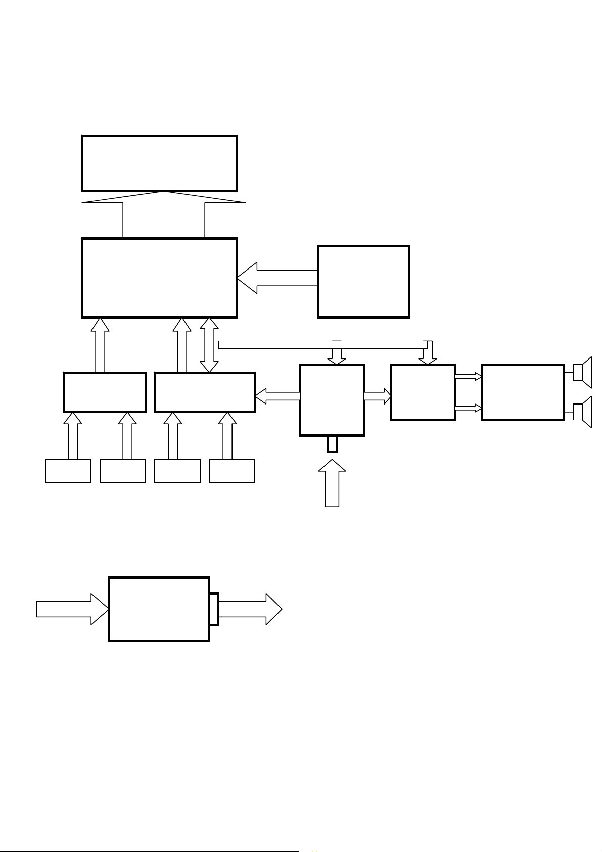
DIAGRAM
US
C
17
CVBS SIF
SWITCH
R
PI5V330Q
LCD PANEL
LVDS OR TTL
GM2221
TVP5147
A/D
FLASH
B
I2C BUS
L
39SF020A
TUNER
PHILIPS
1316
MSP3410
AMPLIFIER
1517
R G B Y U V
AC INPUT 12V D
CVBS Y C
ADAPTER
R
F
Page 18
5
18
GM21 LCD TV__for EU
4
3
2
1
D D
C C
CONTENTS
SCHEMATIC
01. Contents
02. Input
03. GM2221
04.SPI/RESET/KEYPAD
05. LVDS_ Out
06. TTL_ Out
07. Power
08. VIDEO DECODER
SHEET
1
2
3
4
5
6
7
8
B B
Approval
A A
SignatureOrganization
Date
CHY 04-05-17
Title
GM21
Size Document Number Rev
Date: Sheet
5
4
3
2
040108 chy
B
19Tuesday, October 18, 2005
of
1
Page 19

5
19
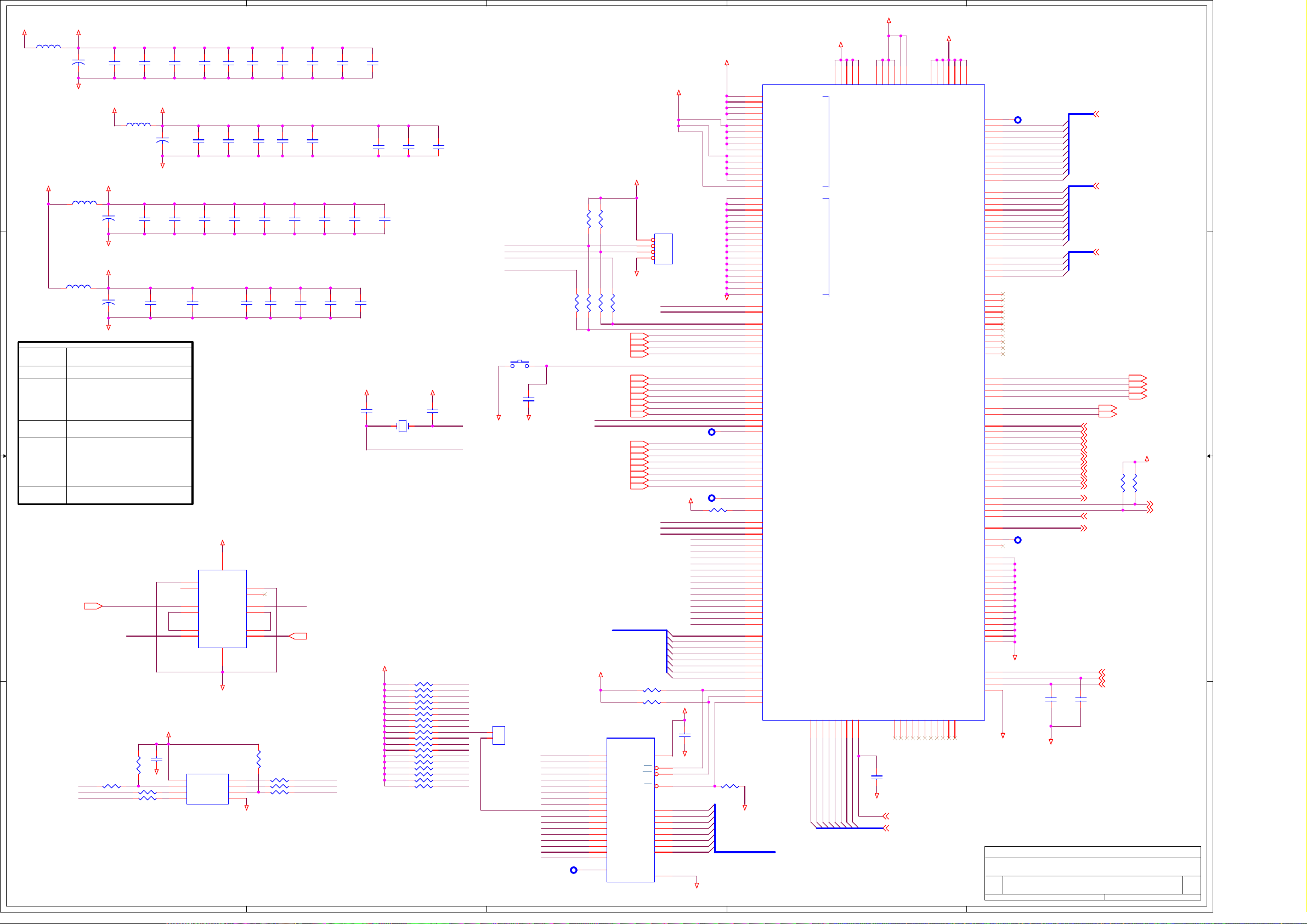
DVI INPUT
4
3
2
1
DVI test points right on the trace to avoid extra length
CONNECTOR
D D
C C
R8
10K
VGASCL
BAV99
1 2
D4
C220
0.1UF
VGASDA
VGA_SCL
VGA_SDA
+5V
BAV99
1 2
GND
A-VS
R12 10K
R13 0R
CN2
GND
15
14
13
12
11
+5V
D7
3
3
BAV99
1 2
GND
R30
10K
GND
GND
R31
10K
5
10
4
9
3
8
2
7
1
6
DB15 HD
D8
R23 20R
1%
1%
GND
Near VGA pins
VGACON
R14
10K
VGA_5V
R?
10K
A-BLUE
A-GREEN
A-RED
HSYNC 5
VSYNC 5 BLUE+ 5
4
RMADDR8 3
For update
VGA RGB In
R1982
R2082
R2182
+5V_MUX
GND
GND
GND
A-Y
10uF/16V
82
R36
GND GND
A-GREEN
10uF/16V
A-PB
GND
R?
GND
C11
12
C15
12
10uF/16V
82
R32
C?
10uF/16V
82
C17
12
GND
R24
BC847c
R33
12
22k
10k
R42
22k
BC847c
R45
10k
22k
Q1
1
Q4
R47
BC847c
R50
R?
BC847c
R?
10k
1
22k
10k
2 3
+5V_MUX
Q6
1
Q?
1
330
R?
SEL_RGB3
2 3
+5V_MUX
2 3
+5V_MUX
2 3
GND
Y/G
R29
1k
GND
R?
75
R37
+5V
3
GND
R17 100R
R18 100R
GND
DNP
+5V
GND
R16
4K7
D6
3
BAV99
1 2
BAT54C
GND
D5
C
5V_VGA
C2
0.1uF
+5V
A2
R15
4k7
GND
5
VGA_5V
A1
EDID VGA
U2
2
A1A2WP
3
4
GND
24AA02
GND
ANALOG DDC
B B
A A
VCCA0
SCL
SDA
81
7
6
5
Pb/B
1k
GND
R10 100R
R11 100R
U3
1
IN
2
SA1
3
SA2
4
DA
5
SB1
6
SB2
7
DB
8
GND
PI5V330
13-PI5V33-0QB
2 3
Vin2
8
3
VCC
EN
SD1
SD2
DD
SC1
SC2
DC
1
Q5
BC847c
+5V_MUX
R48
GND
16
15
14
13
12
11
10
9
+5V_MUX
GND
1k
GND
R46
22k
1 2
10uF/16V
10k
L1
33R FB
Pr/R
R34
A-BLUE
C16
GND
R9
10K
+
C4
2 3
+5V_MUX
10uF
Q2
BC847c
1
R35
10k
Q3
2 3
+5V
BC847c
C5 0.01uF
R41
22k
1
R43
10k
NOT TO BE MOUNTED
+5V_MUX
R26
22k
C13
1 2
10uF/16V
82
1 2
10uF/16V
GND
R49
C14
GND
A-PR
A-RED
2
Pr/R
R22 47R 1%
Y/G
R25 47R 1%
Pb/B
R28 47R 1%
DDC_SCL_VGA 5
DDC_SDA_VGA 5
MUXED RGB
TO 5221ADC
C3 0.01uF
C6 0.01uF
C7 0.01uF
C8 0.01uF
C9 0.01uF
C10 0.01uFR27 20R
C12 0.01uF
R3884.5 1%
R3984.5 1%
R4084.5 1%
GND GND GND
Title
GM21-input
Size Document Number Rev
040108 chy
C
Date: Sheet
INPUT
1
SOG_MCSS 5
RED+ 5
RED- 5
GREEN+ 5
GREEN- 5
BLUE- 5
29Tuesday, October 18, 2005
of
Page 20
5
20
+3.3V_AVDD
L2
33R FB
D D
+1.8V_DVDD
C C
RMADDR[6:0]
RMADDR[12:7]
RMADDR[14:13]
RMADDR15
RMADDR16
RMADDR17
B B
A A
3.3V_AVDD
C18
22uF/16V
GND
L4
33R FB
L5
33R FB
BootStrap Signals
For I2C address [6:0] to JTAG bridge
Host I/F, to determine device address.
User_Bits[5:0] for configuration setting
OP_MODE[1:0]:
00 = Normal op. UART in 186 on system pins.
01 = I2C to JTAG bridge.
10 = JTAG port, 5 wires
11 = External parallel control bus using
ROM Addr/Data
SPI_EN: 0 = parallel ROM I/F. 1 = SPI
serial ROM and Cache control
Initial state of OCM ROM:
0 = internal ROM on, and mapped to top 32K
of OCM and OCM boot will be from internal
ROM codes.
1 = Internal ROM off. The external ROM
mapped to entire upper 512K of OCM address.
OCM boot from external ROM code.
OSC_SEL: 0 = Xtal and internal oscillator.
1 = TTL oscillator (on TCLK pin)
HSYNC3
HOLD
RMADDR16
C19
0.1uF
+3.3V_DVDD 3.3V_DVDD
L3
33R FB
CVDD_1.8
C38
22uF/16V
GND
AVDD_1.8
C48
22uF/16V
GND
VGAHS
R?4K7
100R?
5
Close to respective power Pins
C20
0.1uF
C21
0.1uF
C22
0.1uF
Close to respective power Pins
C29
22uF/16V
GND
C30
0.1uF
Close to respective power Pins
C40
0.1uF
8
7
6
C50
0.1uF
1
2
3
4
11
10
74LCX14
U?
VCC
#HOLD
SCK
C41
0.1uF
3.3V_AVDD
U5
1
2
3
4
11
10
#CE
#WP
VSSSI
14
7
GND
SO
C62
0.1uF
C39
0.1uF
C49
0.1uF
3.3V_DVDD
GND
100R?
100R?
SPI:SST25VF040
SOP8
C23
0.1uF
C31
0.1uF
C42
0.1uF
C24
0.1uF
C32
0.1uF
C43
0.1uF
C25
0.1uF
C33
0.1uF
C44
0.1uF
C26
0.1uF
C34
0.1uF
C45
0.1uF
Close to respective power Pins
C52
C51
0.1uF
14
13
13
12
12
8
8
9
9
6
6
5
5
7
R?4K7
1
2
3
45
GND
0.1uF
VGAVS
100R?
100R?
100R?
C53
0.1uF
VSYNC
3
ROM_CSn
RMADDR15
WPRMADDR17
4
C28
C27
0.1uF
0.1uF
Close to respective power Pins
C35
0.1uF
C46
C47
220pF
220pF
C55
C54
220pF
0.1uF
3.3V_AVDD
C58
X1
5pF
14.318MHz
BOOTSTRAP OPTIONS SELECT
(NOT POPULATED SHOULD BE
HARD WIRED)
+5V
4
C36
0.1uF
3.3V_AVDD
C37
0.1uF
JTAG
DEBUG
I2C SEL
C59
5pF
TCLK
XTAL
RMADDR0
10KR54
RMADDR1
10KR55
RMADDR2
10KR57
RMADDR3
10KR58
RMADDR4
10KR60
RMADDR5
10KR61
RMADDR6
10KR62
RMADDR7
10KR63
10KR64
RMADDR9
10KR65
RMADDR10
10KR66
RMADDR11
10KR67
RMADDR12
10KR68
RMADDR13
10KR69
RMADDR14
10KR70
RMADDR15
10KR71
RMADDR16
10KR72
RMADDR17
10KR73
HOST_SDA/UART_DO
HOST_SCL/UART_DI
DDC_SCL_VGA
DDC_SDA_VGA
SW1
SW PUSHBUTTON
GND GND
T2
For_Update
1
2
C57
0.1uF
RMADDR17
RMADDR16
RMADDR15
RMADDR14
RMADDR13
RMADDR12
RMADDR11
RMADDR10
RMADDR9
RMADDR8
RMADDR7
RMADDR6
RMADDR5
RMADDR4
RMADDR3
RMADDR2
RMADDR1
RMADDR0
TP14 VP
3
R5110K
R5210K
OR30R
OR20R
OR10R
DDC_SCL_VGA3
DDC_SDA_VGA3
DDC_SCL_DVI3
DDC_SDA_DVI3
BLUE+3
BLUE-3
SOG_MCSS3
GREEN+3
GREEN-3
RED+3
RED-3
VGAHS
VGAVS
RX2+3
RX2-3
RX1+3
RX1-3
RX0+3
RX0-3
RXC+3
RXC-3
+5V
U6
30
2
3
29
28
4
25
23
26
27
5
6
7
8
9
10
11
12
1
AT49HF/F010-45JC
32-Pin PLCC Socket
3
OR40R
RMDATA[0..7]
NC/A17
A16
A15
A14
A13
A12
A11
A10
A9
A8
A7
A6
A5
A4
A3
A2
A1
A0
NC
+5V
J1
1
2
3
4
RS232
GND
DDC_SCL_VGA
DDC_SDA_VGA
DDC_SCL_DVI
DDC_SDA_DVI
RESET
R56 10K
R59 10K
32
VCC
24
OE
31
WE
22
CE
21
DQ7
20
DQ6
19
DQ5
18
DQ4
17
DQ3
15
DQ2
14
DQ1
13
DQ0
16
GND
3.3V_AVDD
GPROBE
DEBUG
PORT
TCLK
XTAL
ADC_TEST
RX2+
RX2RX1+
RX1RX0+
RX0RXC+
RXC-
3.3V_AVDD
R53 250/1%
RMADDR17
RMADDR16
RMADDR15
RMADDR14
RMADDR13
RMADDR12
RMADDR11
RMADDR10
RMADDR9
RMADDR8
RMADDR7
RMADDR6
RMADDR5
RMADDR4
RMADDR3
RMADDR2
RMADDR1
RMADDR0
RMDATA7
RMDATA6
RMDATA5
RMDATA4
RMDATA3
RMDATA2
RMDATA1
RMDATA0
+5V
C62
0.1uF
GND
RMDATA7
RMDATA6
RMDATA5
RMDATA4
RMDATA3
RMDATA2
RMDATA1
RMDATA0
GND
3.3V_DVDD
GND
TP10
TP11
ROM_OEn
ROM_WEn
ROM_CSn
SOCKET:
IC51-2084-1052
R74
10K
GND
RMDATA[0..7]
2
AVDD_1.8
3.3V_DVDD
5073190
205
U4
AVDD_OUT_LV_E_33
24
AVDD_OUT_LV_E_33
26
AVDD_LV_33
27
AVDD_OUT_LV_O_33
40
AVDD_OUT_LV_O_33
113
AVDD_IMB_33
120
AVDD_RX2_33
125
AVDD_RX1_33
130
AVDD_RX0_33
134
AVDD_RXC_33
141
AVDD_BLUE_33
145
AVDD_GREEN_33
150
AVDD_RED_33
154
AVDD_ADC_33
172
LBADC_VDD_33
171
AVDD_RPLL_33
12
AVSS_OUT_LV_E
23
AVSS_OUT_LV_E
AVSS_LV
28
AVSS_OUT_LV_O
39
AVSS_OUT_LV_O
115
AGND_IMB
117
AGND_RX2
122
AGND_RX1
127
AGND_RX0
131
AGND_RXC
144
AGND_BLUE
149
AGND_GREEN
153
AGND_RED
156
AGND_ADC
168
AGND_RPLL
177
LBADC_GND
136
GND_RXPLL
170
TCLK
169
XTAL
71
HOST_SCL/UART_DI
72
HOST_SDA/UART_DO
77
DDC_SCL_VGA
78
DDC_SDA_VGA
79
DDC_SCL_DVI
80
DDC_SDA_DVI
178
RESETn
142
BLUE+
143
BLUE-
146
SOG_MCSS
147
GREEN+
148
GREEN-
151
RED+
152
RED-
181
HSYNC
182
VSYNC
155
ADC_TEST
118
RX2+
119
RX2-
123
RX1+
124
RX1-
128
RX0+
129
RX0-
132
RXC+
133
RXC-
138
CLKOUT
114
REXT
183
ROM_ADDR17
184
ROM_ADDR16
185
ROM_ADDR15
186
ROM_ADDR14
187
ROM_ADDR13
188
ROM_ADDR12
189
ROM_ADDR11
192
ROM_ADDR10
193
ROM_ADDR9
194
ROM_ADDR8
195
ROM_ADDR7
196
ROM_ADDR6
197
ROM_ADDR5
198
ROM_ADDR4
199
ROM_ADDR3
200
ROM_ADDR2
201
ROM_ADDR1
202
ROM_ADDR0
203
ROM_DATA7
204
ROM_DATA6
207
ROM_DATA5
208
ROM_DATA4
1
ROM_DATA3
2
ROM_DATA2
3
ROM_DATA1
4
ROM_DATA0
5
ROM_OEn
6
ROM_WEn
7
ROM_CSn
VDATA7/GPIO16
gm2221
PQFP-208
Route (LBADC_IN1, LBADC_RET) and
(LBADC_IN2, LBADC_RET) as differential
tracks close to each other and ground the
return track of each pair very close to the
5221 and ground pin
102
YUV7
95
RVDD_33
RVDD_33
RVDD_33
RVDD_33
RVDD_33
3.3V_A
AGND
VDATA6/GPIO17
VDATA5/GPIO18
VDATA4/GPIO19
VDATA3/GPIO20
VDATA2/GPIO21
VDATA1/GPIO22
VDATA0/GPIO23
VCLK
103
106
107
108
109
110
111
112
YUV2
YUV6
YUV0
YUV1
YUV5
YUV4
YUV3
GND
DECCLK
YUV[0..7]
2
166
116
12125126
13711164
VDD_RX1_18
VDD_RX0_18
VDD_RX2_18
VDD1_ADC_18
VDD_RXPLL_18
NCNCNCNCNCNCNCNCNC
54
5253104
C63
8P2
DECCLK
YUV[0..7]
VDD_RPLL_18
NC
CVDD_1.8
CVDD_1.8
94175
96
86
139
179
CVDD_18
CVDD_18
CVDD_18
CVDD_18
CVDD_18
CVDD_18
PD20/EB4
PD21/EB5
PD22/EB6
PD23/EB7
PD24/OR0
PD25/OR1
PD26/OR2
PD27/OR3
PD28/OR4
PD29/OR5
PD30/OR6
PD31/OR7
PD32/OG0
PD33/OG1
PD37/OG5
GPIO7/IRQin
GPIO8/IRQout
GPIO9/SCL
GPIO10/SDA
PWM0/GPIO11
PWM1/GPIO12
PWM2/GPIO13
PWM3/GPIO14
STI_TM1/GPIO15
VBUFC_RPLL
VBUFC_DVI
GND_RPLL
GND1_ADC
LBADC_IN1
LBADC_IN2
LBADC_IN3
LBADC_RETURN
NC
158
159
160
161
162
VCO_LV
DCLK
PPWR
PBIAS
GPIO0
GPIO1
GPIO2
GPIO3
GPIO4
GPIO5
GPIO6
STI_TM2
CRVSS
CRVSS
CRVSS
CRVSS
CRVSS
CRVSS
CRVSS
CRVSS
CRVSS
CRVSS
CRVSS
CRVSS
CH3P_LV_E(PD0/ER0)
CH3N_LV_E(PD1/ER1)
CLKP_LV_E(PD2/ER2)
CLKN_LV_E(PD3/ER3)
CH2P_LV_E(PD4/ER4)
CH2N_LV_E(PD5/ER5)
CH1P_LV_E(PD6/ER6)
CH1N_LV_E(PD7/ER7)
CH0P_LV_E(PD8/EG0)
CH0N_LV_E(PD9/EG1)
CH3P_LV_O(PD10/EG2)
CH3N_LV_O(PD11/EG3)
CLKP_LV_O(PD12/EG4)
CLKN_LV_O(PD13/EG5)
CH2P_LV_O(PD14/EG6)
CH2N_LV_O(PD15/EG7)
CH1P_LV_O(PD16/EB0)
CH1N_LV_O(PD17/EB1)
CH0P_LV_O(PD18/EB2)
CH0N_LV_O(PD19/EB3)
105
157
1
CVDD_18
DEN
DHS
DVS
10
13
14
15
16
17
18
19
20
21
22
29
30
31
32
33
34
35
36
37
38
43
44
45
46
56
57
58
59
60
61
62
63
64
65
66
47
48
49
55
67
68
81
82
83
84
85
88
89
90
91
92
93
98
99
100
101
69
167
135
70
206
191
180
140
97
94
76
74
51
42
8
87
165
163
TP9
TP12
LV_E9
LV_E8
LV_E7
LV_E6
LV_E5
LV_E4
LV_E3
LV_E2
LV_E1
LV_E0
LV_O9
LV_O8
LV_O7
LV_O6
LV_O5
LV_O4
LV_O3
LV_O2
LV_O1
LV_O0
PD20
PD21
PD22
PD23
GPIO0
GPIO1
GPIO2
GPIO3
GPIO5
GPIO6
MCSCL
MCSDA
PPWR
PBIAS
SEL_RGB
VGACON
RET_OTHER
LED
WP
HOLD
AMP_MUTE & 9V suspend
IR_IN
SWTCH3
MCSCL
MCSDA
PWM0
BLNK2
TELE_INR
KEYBOARD
LV_E[0..9] 7,8
LV_O[0..9] 7,8
PD[20..23] 8
DEN
DHS
DVS
DCLK
PPWR 7,8
PBIAS 7
DIFFERENT FOROM EM & CHINA
3.3V_DVDD
R?4K7
R?4K7
DEN
DHS
DVS
DCLK
INPUT TO
C60
0.1uF
GND
LBW ADC
ADC_IN1
SWTCH1
SWTCH2
C61
0.1uF
1
39Tuesday, October 18, 2005
GND
173
174
175
176
LBADC_RET
GND
Title
GM21-gm5221
Size Document Number Rev
040108 chy
C
Date: Sheet
TELE_SDA
TELE_SCL
of
Page 21
5
21
4
3
2
1
D D
Keypad
INTERFACE
NV RAM
INTERFACE
+5V
R76
4K7
MCSCL
MCSDA
C C
IR REMOTE SENSOR
INTERFACE
B B
J7
1
2
3
4
5
CON5
A A
5
+5V
GND
+5V
GND
C66
220pF
R75
10K
C64
220pF
LED
IR_IN
GND
ADC_IN1
4
GPIO9/SCL
GPIO10/SDA
J3
CON15
J?
1
2
3
CON3
x2.0mm
J8
1
2
3
4
5
CON5
J?
CON2
3
1
2
new
1
2
3
4
5
6
7
8
9
10
11
12
13
14
15
GND
GND
R77
4K7
CVBS2
CVBS1
SVIDEO_Y
SVIDEO_C
+9V
+9V
C67
0.1uF
C65
0.1uF
GND GND
CVBS2
CVBS1
SVIDEO_Y
SVIDEO_C
Vin2
Vout2
TELE_INR
MCSCL
MCSDA
+5V
C68
0.1uF
+12V
8
7
6
C69
0.1uF
U7
VCC
WP
SCK
24LC16B
CON5
J4
VSSSI
A0
A1
A2
1
2
3
4
5
J6
CON6
1
2
3
45
SWICH1
SWICH3
AMP_MUTE
RET_OTHER
GND
EXTERAL AV
BOARD
INTERFACE
2
Audio_InR2
Audio_InL2
Audio_OutR2
Audio_OutL2
1
2
3
4
5
6
Title
GM21- connectors
Size Document Number Rev
Date: Sheet
040108 chy
B
49Tuesday, October 18, 2005
of
1
Page 22
5
22
+5V
4
+12V
L6
L8
3
Backlight
Inverter
+5V
2
1
Connector
R79
2K
R80 470R
3
D D
PWM0
R82 1K
Q7
1
MMBT3904L
2
GND
C72
0.1uF
GND
BKLT_ADJ
C73
22uF/16V
C70
0.1uF
GND
31R FB
31R FBL731R FB
C71
0.1uF
L9
GND
J9
1
2
3
4
5
6
7
CON7
L10
L11
31R FB
31R FB
31R FB
GND
BKLT_ENBKLT_EN
R81 0R
4k7
R85 0R
LVDS test points right on the trace to avoid extra length
LV_O[0..9]
+12V
+5V+3.3V_DVDD
Panel Power Voltage Selection
R87
C C
R90
PPWR
PPWR5
R91 4K7 C223
3
Q9
1
MMBT3904L
2
GND
R86
0
+5V
R89
47K
1K
C74
0.1uF
R88
0
0
C75
22uF/16V
U8
1
S1
2
G1
3
S2
4
G2
SI9953ADY
8
D1
7
D1
6
D2
5
D2
F1
33R FB
Panel Power Switch
C56
0.1uF
GND GND
PANEL_POWER
0.1uF
LV_E[0..9]
TXO0-
TXO0+
TXO1-
TXO1+
TXO2-
TXO2+
TXOC-
TXOC+
TXO3-
TXO3+
LV_O0 TXO0-EB3
EB2
LV_O2
EB1
LV_O3 EB0
LV_O4 EG7
LV_O5 EG6
LV_O6 EG5
LV_O7 EG4
LV_O8 EG3
LV_O9 EG2
TXE0+
R78
10K
3
2
MMBT3904L
GND
LV_E0 EG1
LV_E1 EG0
R84 1KR83
1
Q8
PBIAS
PBIAS 5
TXO0+LV_O1
TXO1TXO1+
TXO2TXO2+
TXOCTXOC+
TXO3TXO3+
TXE0TXE0+
TXE1TXE1+
TXE2TXE2+
TXECTXEC+
TXE3TXE3+
PANEL_POWER
TP15
CN3
30
29
28
27
26
25
24
23
22
21
20
19
18
17
16
15
14
13
12
11
10
9
8
7
6
5
4
3
2
1
DF14A-30P-1.25H
LVDS Output
Connector
GND
B B
A A
5
GND
GND
4
3
TXE1-
TXE1+
TXE2-
TXE2+
TXEC-
TXEC+
TXE3-
TXE3+
LV_E2 ER7
LV_E3 ER6
LV_E4 ER5
LV_E5 ER4
LV_E6 ER3
LV_E7 ER2
LV_E8 ER1
LV_E9 ER0
Title
GM21-LVDS out
Size Document Number Rev
040108 chy
C
59Tuesday, October 18, 2005
Date: Sheet
2
1
of
Page 23

5
23
D D
4
3
2
1
PANEL_POWER PANEL_POWER
LV_E[0..9]
C C
LV_O[0..9]
PD[20..23]
B B
DENSHT-5,6
DHSSHT-5,6
DVSSHT-5,6
DCLKSHT-5,6
DEN
DHS
DVS
DCLK
LV_E9
LV_E8
LV_E7
LV_E6 ER3
LV_E5
LV_E4
LV_E3
LV_E2
LV_E1
LV_E0
LV_O9
LV_O8
LV_O7
LV_O6
LV_O5
LV_O4
LV_O3
LV_O2
LV_O1
LV_O0
PD20
PD21
PD22
PD23
R92 22R
R93 22R
R94 22R
R95 22R
22Rx4
22Rx4
22Rx4
8
7
6
5 4
8
7
RN1
6
5 4
8
7
6
5 4
8
7
6
5 4
8
7
6
5 4
8
7
6
5 4
1
2
3
1
2
3
1
2
3
1
2
3
1
2
3
1
2
3
RN222Rx4
RN3
RN422Rx4
RN5
RN622Rx4
ER0
ER1
ER2
ER4
ER5
ER6
ER7
EG0
EG1
EG2
EG3
EG4
EG5
EG6
EG7
EB0
EB1
EB2
EB3
EB4
EB5
EB6
EB7
DE
HS
VS
CLK
ER[0..7] SHT-6
EG[0..7] SHT-6
EB[0..7] SHT-6
CLK
VS
EB6
EB2
EB0 EB1
EG6
EG4
EG2
EG0
ER6
ER4
ER2
ER0
J10
1
3
5
7
9
11
13
15
17
19
21
23
25
27
29
31
33
35
37
39
87089-40
2
4
6
8
10
12
14
16
18
20
22
24
26
28
30
32
34
36
38
40
DE
HS
EB7
EB5EB4
EB3
EG7
EG5
EG3
EG1
ER7
ER5
ER3
ER1
GNDGND
C76
47PF
GND
A A
Title
GM21-TTL out
Size Document Number Rev
Date: Sheet
5
4
3
2
040108 chy
B
69Tuesday, October 18, 2005
of
1
Page 24
5
24
4
3
2
1
D12
L21
33R FB
GND
1N4001
U9
LM2596S-5.0
1
VIN
C105
100uF/16V
C111
100uF/16V
31ohm at 100Mhz Rated Currrent
>=2A
2
VOUT
GND
3
GND
C95
100uF/16V
C106
0.1uF
ADJONTAB
456
lt1084-3.3V
U10
3 2
VIN VOUT
LT1117-3.3V
U12
3 2
VIN VOUT
Sot223
GND/ADJ
GND
D9
IN5820
1 2
TAB
1
GND/ADJ
1
GND
TAB
L15
33uH
4
4
C82
330uF/16V
C83
330uF/16V
C84
0.1uF
C93
0.1uF
GND
U13
C112
0.1uF
LT1117-1.8V
3 2
VIN VOUT
GND/ADJ
Sot223
4
TAB
1
L13 33R FB
L16 33R FB
L17 33R FB
L18 33R FB
L19 33R FB
L20 33R FB
40mA
C94
100uF/16V
10V
GND
C103
0.1uF
GND
GND GND
GND
C109
0.1uF
C85
100uF/16V
330uF/16V
+3.3V_AVDD
200mA
C104
100uF/16V
+1.8V_DVDD
CVDD:300mA
AVDD:60mA
C110
100uF/16V
C86
0.1uF
+5V
GND
C87
JP1
4
3
2
1
POWER IN
+5V
L23
33R FB
+3.3V_AVDD +3.3V_LBADC
L25
33R FB
C88
0.1u
+9V
+5V_MUX
C102
22uF/16V
GND
C108
22uF/16V
GND GND
GND
GND
C107
0.1uF
C89
100P
C96
0.1uF
C101
0.1uF
C91
470uF/25V
GNDGND
R96
+12V
GNDGND
C97
100uF/16V
10V
U11
C92
0.1u
100
RELA1
4
3
Jidian1
KIA278R09
VOUT
GND
To-223
324
BC847c
Q10
2
1
GND
C77
0.1u
R98
C90
0.1u
C98
0.1uF
2k2
GND
L22
33R FB
C99
100uF/16V
10V
D10
1N4148
GND
1
Vin
SW
R97
10k
1
2 3
C100
0.1uF
GND
POWER
J11
1
2
CONTROL
+12V
+12V
L12 33R FB
L14 33R FB
C79
C78
D D
470uF/25V
100uF/16V
C C
+5V
L24
33R FB
+5V
L26
33R FB
B B
C81
C80
0.1uF
0.1uF
+5V +3.3V_DVDD
D11
1N4001
GND
+3.3V_AVDD
L27
33R FB
C115
100uF/16V
GND
A A
C116
0.1uF
GND
U14
LT1117-1.8V
3 2
Sot223
TAB
VIN VOUT
GND/ADJ
1
GND
+1.8V_DEC
A_1.8V
L28
L29
33R FB
33R FB
D_1.8V
Title
4
C113
0.1uF
GND
C114
100uF/16V
GND
GM21-power
Size Document Number Rev
040108 chy
C
79Tuesday, October 18, 2005
Date: Sheet
5
4
3
2
1
of
Page 25
5
25
4
3
2
1
J12
1
2
3
4
5
6
7
8
9
10
L30 2.7uH
L34 2.7uH
120
CON10
L35 2.7uH
GND
L46 2.7uH
C120
330pF
GND
C127
330pF
GND
C141
330pF
D D
R103
CVBS2
CVBS2
120
C119
4.7pF
R104 NC
GND
CVBS1
GND
CVBS1
R105
120
C126
4.7pF
R106 NC
GND
SVIDEO_C
SVIDEO_C
GND
R108
C140
4.7pF
R109 NC
GND GND
GND
C C
SVIDEO_Y
SVIDEO_Y
C147
4.7pF
R110
120
L36 2.7uH
C148
330pF
R111 75R 1%
TV_IN
TV_IN
GND
R112
120
C157
4.7pF
R113 NC
GND GND
GND
L37 2.7uH
GNDGND
C158
330pF
DECBIN
DECGIN
DECRIN
DEC_FB
R? 0
R? 0
FOR TELETEXT
L49 2.7uH
L47 2.7uH
L51 2.7uH
L50 2.7uH
R44
NC
SCART_R
SCART_CVBS/Y
SCART_R
SCART_G
SCART_B
DECODER_VS
DECODER_HS
R99 100R
R100 100R
R107
0
GND
SCART_G
GND
SCART_B
GND
CVBS_OUT
C123 0.1uF
C225 0.1uF
C128 0.1uF
C130 0.1uF
C142
330pF
C144 0.1uF
C145 0.1uF
C146 0.1uF
C149
330pF
C154 0.1uF
C155 0.1uF
C156
330pF
GND
C163 0.1uF
C164
330pF
GND
TELE_SDA
TELE_SDA
C121
0.1uF
GND
C224
330pF
C228
330pF
GND
C229
330pF
GND
GND
GND
C122
0.1uF
C226
330pF
C227
330pF
A_3.3V
A_1.8V
GND
GND
33pF
10
11
12
13
14
15
16
17
18
19
20
C117
C118
33pF
1
2
3
4
5
6
7
8
9
14.318Mhz
12
X2
80
VI_1_A
CH1_A18GND
VI_1_B
VI_1_C
CH1_A33GND
CH1_A33VDD
CH2_A33VDD
CH2_A33GND
VI_2_A
VI_2_B
VI_2_C
CH2_A18GND
CH2_A18VDD
A18VDD_REF
A18GND_REF
CH3_A18VDD
CH3_A18GND
VI_3_A
VI_3_B
VI_3_C
CH4_A33GND
CH4_A33VDD
R101 100K
R102 10K
GND
DVDD
XTAL1
XTAL2
PLL_A18VDD
PLL_A18GND
CH1_A18VDD
DGND
C-2/GPIO
FID/GPIO
C_1/GPIO
C_0/GPIO
HS/CS/GPIO
VS/VBLK/GPIO
C_5/GPIO
C_4/GPIO
C_3/GPIO
C_7/GPIO/GREEN
U15
TVP5147PFP
CH4_A33VDD
CH4_A33GND
VI_4_A
CH4_A18GND
CH4_A18VDD
NSUB
TMS
SCL
SDA
INTREQ
DVDD
DGND
PWDN
RESETB
21222324252627282930313233343536373839
R120
100R
61626364656667686970717273747576777879
IOVDD
IOGND
C_6/GPIO/RED
C_8/GPIO/BLUE
C_9/GPIO/FSO
DGND
DVDD
IOGND
IOVDD
DGND
DVDD
FSS/GPIO
AVID/GPIO
GLCO/I2CA
IOVDD
IOGND
DATACLK
40
R115
10K
GND
Y_0
Y_1
Y_2
Y_3
Y_4
Y_5
Y_6
Y_7
Y_8
Y_9
DECODER_VS
DECODER_HS
TP16
TP17
TP18
D_3.3V
D_1.8V
+3.3V_DVDD
L32
33R FB
C124
0.1uF
L31 33R FB
L33 33R FB
C125
100uF/16V
10V
A_3.3VD_3.3V
GND GND
D_3.3V A_3.3V
C?
10P
8
7
6
8
7
6
DECBIN
DECGIN
DECRIN
DEC_FB
C?
10P
R114 22R
YUV0
YUV1
YUV2
YUV3
YUV4
YUV5
YUV6
YUV7
C133
0.1uF
C134
0.1uF
YUV[0..7]
C135
0.1uF
DECCLK
GNDGND
C136
0.1uF
A_1.8V
C150
0.1uF
GND
D_1.8V
C159
0.1uF
C137
0.1uF
C151
0.1uF
C160
0.1uF
C138
0.1uF
C152
C161
0.1uF
0.1uF
C139
0.1uF
C153
0.1uF
C162
0.1uF
C129 0.1uF
60
C131 0.1uF
59
C132 0.1uF
58
57
56
55
54
53
52
51
50
49
48
47
46
45
44
43
42
41
GND
C143
10P
GND GND GND
C?
10P
RN7
22Rx4
1
2
3
4 5
RN8
1
2
3
4 5
22Rx4
GND
B B
R118 100R
A A
R116 100R
R117 100R
RET_OTHER
MCSDA
MCSCL
Title
GM21-Video decoder
Size Document Number Rev
040108 chy
C
89Tuesday, October 18, 2005
Date: Sheet
5
4
3
2
1
of
Page 26

5
26
AV1-R PC_LPC_R
R534
0
AV1-L
R535
0
R536
NC
R537
NC
R538
0
R539
0
4
3
2
1
LCD20V6AT.Analog
C536
10u 25v
0
IC502
AVSUP
ANA-IN+
ANA-INANA-IN2+
TESTEN
XTAL-IN
XTAL-OUT
TP
AUD-CL-OUT
NC
NC
D-CTR-I/O1
D-CTR-I/O0
ADR-SEL
STANDBYQ
NC
L504
Q701
3904
R705
470
LNA SW
C553
0
AFT
C552
1n
0
C537
10u 25V
C508
C713
R720
100uH
C512
10n
+5V
47P
R702
22K
NS
R776
NS
L505
C513
47U 25V
0
0
R502
22K
68K NC
SOT-23
+5V
0
C518
3.3P
+5V
470U 16V
R708
R719
47K
Q703
R725
C511
10u 25v
C515
56P
C516 10n
C517 56P
C519
3.3P
R506
100
C509
103
R503
10K
C703
R779
180K
C779
NS
TUNER-L/R
R721
0
8.2k NS
5
0
18.433M1
0
+5V
R711100
R714100
C728
103
R780
2.4K NS
C510
100n PE
X501
R504
Q501
3904
R505
330
R701
22K
R704
22K
10
C705
0.01UF
MSP3410G
49
50
51
52
53
54
55
56
57
58
59
60
61
62
63
64
R507
10k
R508
100
D D
0
C C
C507
47P
R501
220
B B
VIDEO
AFT
GND
TU
NC
MB
RF AGC
SDA
TU1
SCL
GND
SIF OUT
AUDIO
A A
NC
NC
IF AGC
LNA SW
LNA B
TU701
L503
12uH
17
16
15
+31V
14
13
12
11
10
9
C780
8
NS
7
6
10U 16V
5
4
3
2
1
C554
1n
484746454442413938
12345678910111213
NC
0
C53510u 25v
NC
43
ASG
AVSS
SC1-IN-L
SC1-IN-R
MONO-IN
VREFTOP
IC204 DIP2 MSP34*5G
I2C-CL
I2C-DA
I2S-CL
I2S-WS
I2S-DA-OUT
I2S-DA-IN1
C534
0
SC2-IN-L
SC2-IN-R
ADR-DA
ADR-WS
40
ASG
ADR-CL
0
SC3-IN-L
SC3-IN-R
DVSUP
DVSS
3u3 25v
ASG
I2S-DA-IN2NCRESETQ
0
C522
C521
103
C523
47u 25v
0
C702 100U 16V
0.01UF
Q702
3904
R707
180
100U 16V
C706
C701
C704
470U 16V
C707
224
U701 RT34063
+9V
L703 100UH
C724
10u 16v
0
C555
NC
C533
353637
SC4_IN_R
14
103
12uH
R744 220
R746
2.2
0
C550
1n
0
34
33
AHVSS
AGNDC
AHVSUP
SC4_IN_L
SC1-OUT-L
SC1-OUT-R
SC2-OUT-L
SC2-OUT-R
DACM-SUB
NC
NC
16
15
C524
0
L701
+5V
C725
224
C556
1n
C532
100n PE
CAPL-M
CAPL-A
VREF1
DACM-L
DACM-R
VREF2
DACA-L
DACA-R
10U 25v
+9V
R706
0
8
7
6
C557
1n
0
C551
1n
C531 1n5
+9V
L
R740 100
C726
22u 50v
C538
C720
47u 50v
1000p
0
0
C530
R516
R510
10K
1
2
3
45
R747
24K/1%
4
100
C525
1000p
47u 25v
0
R520 1K
0
C723
150P
D501
1N4148
0
70v
D701 IN4148
2 1
R752
1k/NS
+30.6V
C727
224
22uH
R
C526
1000p
Q707
847A
L506
C529
470p
0
C528 47u 25v
32
31
30
C527 47u 25v
29
28
27
26
25
24
NC
23
22
NC
21
20
19
18
17
R515 100
0
+5V
R509
1K
LN701 220UH
R741 1K R732
R748
1K/1%
SC
SE
TC
GNDCOMP
DRIVER
IPK
VCC
+5V
Q506
3904
R524
+5V
1K
R523
1K
3904
0
+5V
R517
1K
3904
Q504
R518
1K
0
0
R514
Audio L
1K
R512
J706
CON15
123456789101112131415
CVBS1
SVIDEO-Y
+31V
C722
224
Audio R
1K
TV
SVIDEO-C
SVIDEO-C
Q505
R521
1K
R519
1k
SDA
SCL
22U/16V
C714
+
BCB47
PC_R PC_L
BASS
R522
1k
Audio-OUT R
Q705
1 3
R735
1k
3
Audio-OUT L
+9V
2
10K
R742
82
R710 3K3
R712
6K8
R715 3K3
R716
6K8
J506
1
2
3
4
5
6
R723
22K
C719
C721103
C
1
3 4
22U/16V
C710
22U/16V
R532
103
R533
103
+
22U/16V
Y
2
SZ701
C709
R724
22K
2
R733
10K
R713
100K
R717
100K
L702
102
R743
82
JP702
1
2
3
+12V
R525
J707
CON10
123456789
LNA SW
RS
MUTE
L704
102
+9V
C715
CAP NP
Q706
BCB47
1 3
R734
1k
8
9
7
789
6
456
23
CIRDIN_8-P
1
1R 1/2W
C542
470u/16V
C545
NC
10
AFT
+5V
+9V
+12V
471
471
471
C503
C502
C501
5
4
C539
NC
2u2/16V
+
C543
2n
0 0 0
SVIDEO-Y
C716
+
22U/16V
R736
82
1
AV1-V3
AV701
2
2
C541
R722
R731
R703
330
JP701
+
C548
220uF/25v
+
C549
220uF/25V
C540
2.2uF
+
C544
2.2uF
R526
10k
+9V
22K
Q704
2
C1815
1 3
R737
10K
1k
1
INR
2
SGND
3
SVRR
4
OUTR
5
PGND
6
OUTL
7
VCC
8
M/SW
9
INL
10 11
GND GND
R527
+
C546
47u/16V
Q508
2 3
3904
R528
0
AV1-R AV1-L
R727
1K
CVBS1
1
D504
1N4148
D505
1N4148
IC503
TPA1517
220
R530
1
C718
AV1-V1
100
R529
NC
R728
10K
22U/16V
R738
100K
AR
2
Title
Size Document Number Rev
C
Date: Sheet
8
D503
NC
C547
NC
R729
1K
C717
22U/16V
AL
9
CIRDIN_8-P
R709
330
+12V
R739
100K
7
789
6
456
5
4
FOR LOUNDSPEAKER
1
11Thursday, December 15, 2005
1
2
3
23
1
20
GND
19
GND
18
GND
17
GND
16
GND
15
GND
14
GND
13
GND
12
GND
+
100u/16V
Q5073906 NC
R531 NC
D502
1N4148
R546
R730
10K
1
AV1-V2
2
LCD20V8AT.TuNi.Shematic
<Doc> <RevCode>
CON2
of
CON2
J703
J704
1
2
1
2
Page 27
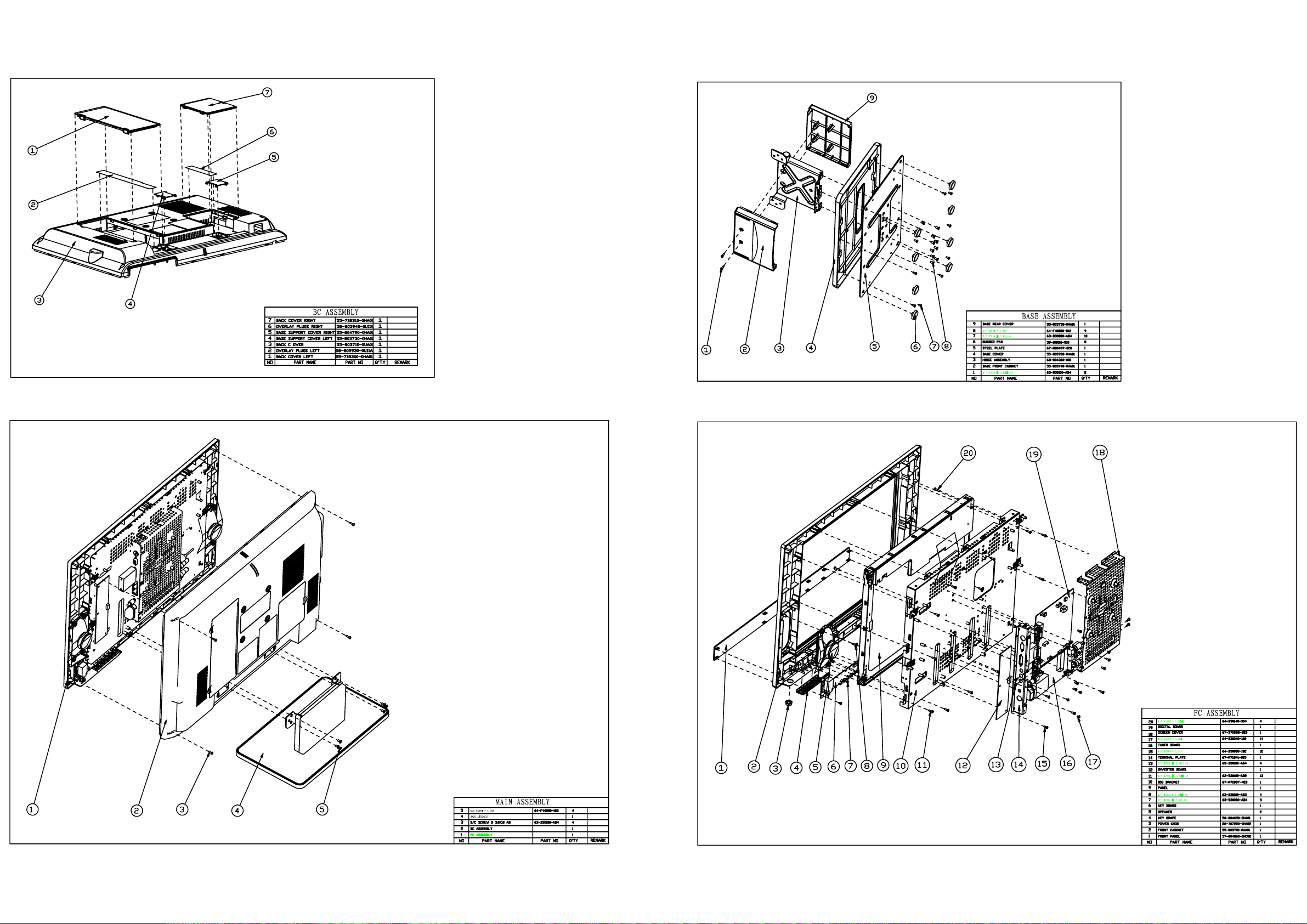
27
 Loading...