

Page 1

TCL
SERVICE MANUAL
L65P1US/MS68A-AP
1. Caution…………………………………………………………………………
2. specification……………………………………………………………………
3. Alignment Procedure…………………………………………………………
4.Block diagram…………………………………………………………………
5.Scheme Diagram ……………………………………………………………
6. Troubleshooting………………………………………………………………
([SORGHGUDZLQJ
This m anual i s t he l atest at t he t ime of pr inting, and doe s not
include the modification which may be made after the printing, by
the constant improvement of product
Page 2
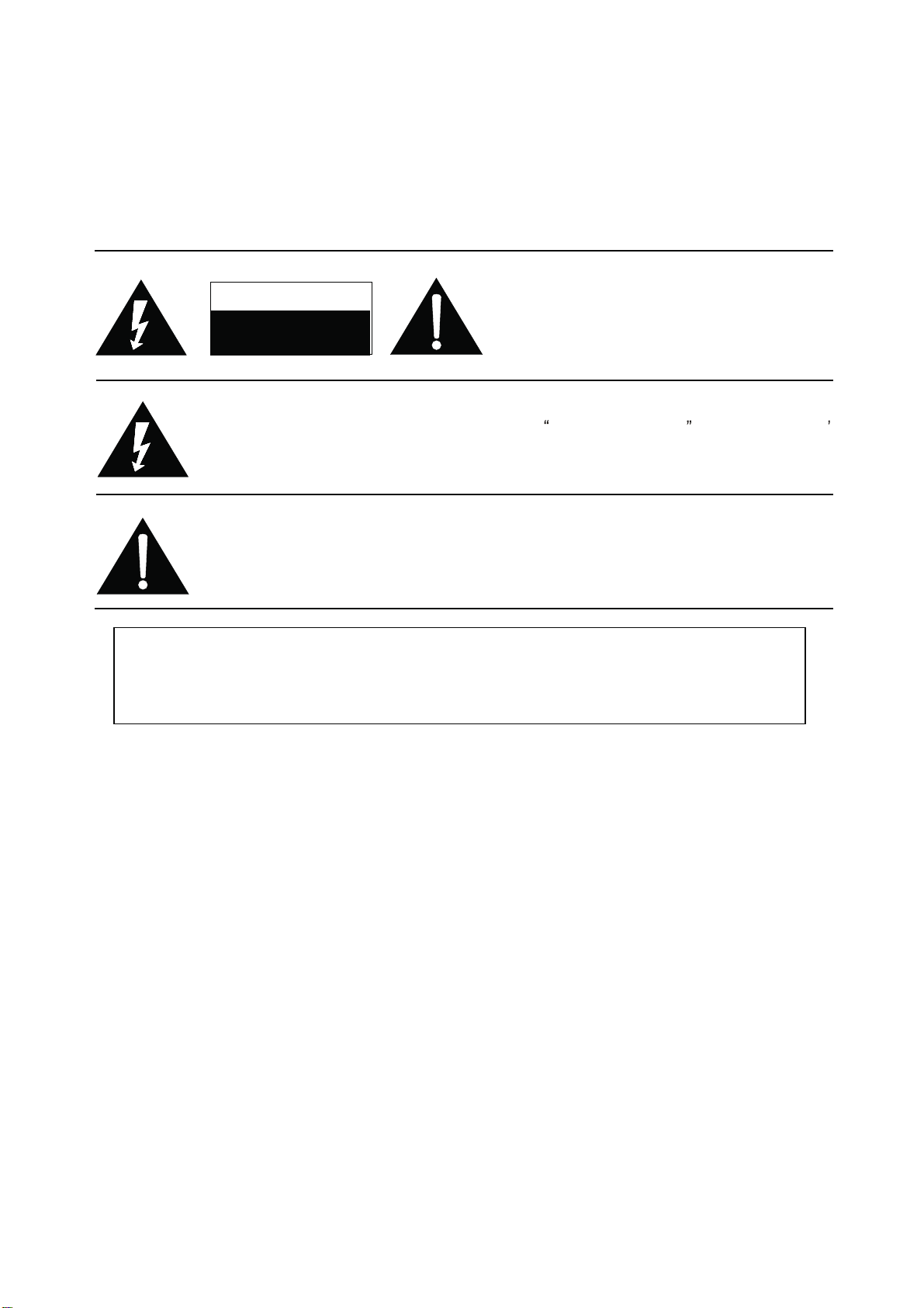
RISK OF
ELECTRIC
SHOCK DO
NOT
OPEN.
SCHNEIDER ELECTRONICS GMBH-GERMANY
1. CAUTION
CAUTION:
Use of controls, adjustments or procedures other than those specified herein may result in
hazardous radiation exposure.
CA UTION : TO RE DUCE THE RIS K OF
CA U T IO N
RISK
SHOCK
The lighting flash with arrowhead symbol, with an equilateral triangle is intended to
alert the user to the presence of uninsulated voltage within the product s
enclosure that may be of sufficient magnitude to constitute a risk of electric shock to
the person.
The exclamation point within an equilateral triangle is intended to alert the user to the
presence of important operating and maintenance (servicing) instructions in the
literature accompanying the appliance.
ELECTRI
NOT
OPEN.
ELECTR ICAL SH OCK, DO NOT REMOVE
COVER (OR BACK). NO USER SERVICEABLE
PAR TS INS IDE . RE FER SER VIC ING TO
QUALIFIE D SERVIC E PERS ONNEL.
dangerous
WARNING: TO REDUCE RISK OF FIRE OR ELECTRIC SHOCK, DO NOT
EXPOSE THIS APPLIANCE TO RAIN OR MOISTURE.
2
2
Page 3

SCHNEIDER ELECTRONICS GMBH-GERMANY
IMPORTANT SAFETY INSTRUCTIONS
CAUTION:
Read all of these instructions. Sa ve these instructions for later use . Follo w all Warnings and
Instructions marked on the audio equipment.
1. Read Instructions-All the safety and operating instructionsshouldbe read before the productis operated.
2. Retain Instructions- The safety and operating instructions should be retained for future reference.
3. Heed Warnings- All warnings on the product and in the operating instructions should be adhered to.
4. Follow Instructions- All operating and use instructions should be followed.
FOR YOUR PERSONAL SAFETY
1. When the power cord or plugis damaged or frayed, unplug this television set from the wall outlet and refer servicing to
qualified service personnel.
2. Do not overload wall outlets and extension cords as this can result in fire or electric shock.
3. Do not allow anything to rest on or roll over the power cord, and do not place the TV where power cord is subject to
traffic or abuse. This may result in a shock or fire hazard.
4. Do not attempt to service this television set yourself as opening or removing covers may expose you to dangerous
voltage or other hazards. Refer all servicing to qualified service personnel.
5. Never push objects of any kind into this television set through cabinet slots as they may touch dangerous voltage
points or short out parts that could result in a fire or electric shock. Never spill liquid of any kind on the television set.
6. If the television set has been dropped or the cabinet has been damaged, unplug this television set from the wall outlet
and refer servicing to qualified service personnel.
7. If liquid has been spilled into the television set, unplug this television set from the wall outlet and refer ser vicing to
qualified service personnel.
8. Do not subject your television set to impact of any kind. Be particularly careful not to damage the picture tube surface.
9. Unplug this television set from the wall outlet before cleaning. Do not use liquid cleaners or aerosol cleaners. Use a
damp cloth for cleaning.
10.1. Do not place this television set on an unstable cart, stand, or table. The television set may fall, causing serious injury
to a child or an adult, and serious damage to the appliance. Use only with a car t or stand recommended by the
manufacturer, or sold with the television set. Wall or shelf mounting should follow the manufacturer s instructions, and
should use a mounting kit approved by the manufacturer.
10.2. An appliance and cart combination should be moved with care. Quick stops, excessive force, and uneven surfaces
may cause the appliance and cart combination to overturn.
3
3
Page 4
SCHNEIDER ELECTRONICS GMBH-GERMANY
PROTECTION AND LOCATION OF YOUR SET
11. Do not use this television set near water ... for example, near a bathtub, washbowl, kitchen sink, or laundry tub, in a
wet basement, or near a swimming pool, etc.
Never expose the set to rain or water. If the set has been exposed to rain or water, unplug the set from the wall
outlet and refer servicing to qualified service personnel.
12. Choose a place where light (artificial or sunlight) does not shine directly on the screen.
13. Avoid dusty places, since piling up of dust inside TV chassis may cause failure of the set when high humidity persists.
14. The set has slots, or openings in the cabinet for ventilation purposes, to provide reliable operation of the receiver, to
protect it from overheating. These openings must not be blocked or covered.
Never cover the slots or openings with cloth or other material.
Never block the bottom ventilation slots of the set by placing it on a bed, sofa, rug, etc.
Never place the set near or over a radiator or heat register.
Never place the set in enclosure, unless proper ventilation is provided.
a built-in
PROTECTION AND LOCATION OF YOUR SET
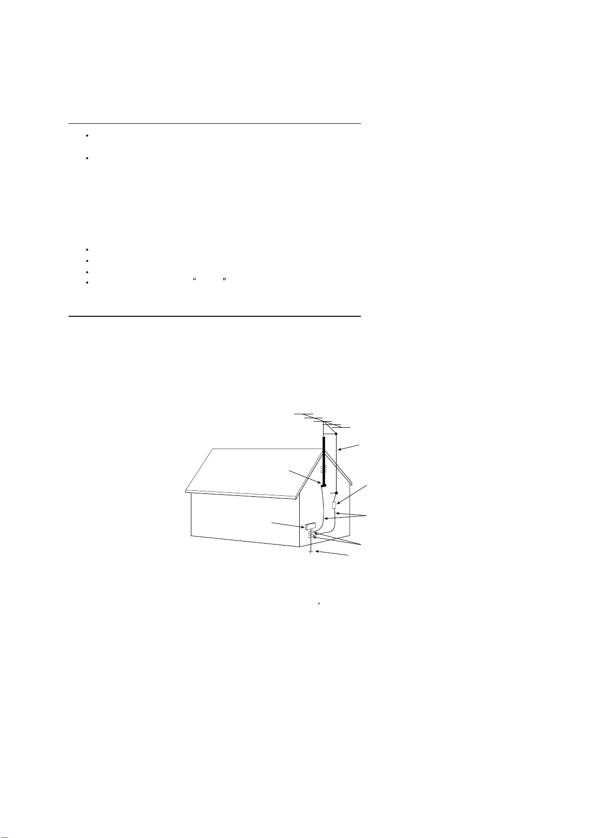
15.1. If an outside antenna is connected to the television set, be sure the antenna system is grounded so as to provide some
protection against voltage surges and built up static charges, Section 810 of the National Electrical Code, NFPA No.
70-1975, provides information with respect to proper grounding of the mast and supportingstructure, grounding of the
lead-in wire to an antenna discharge unit, size of grounding conductors, location of antenna discharge unit, connection
to grounding electrode, and requirements for the grounding electrode.
EXAMPLE OF ANTENNA GROUNDING AS PER NATIONAL ELECTRICAL CODE INSTRUCTIONS
EXAMPLE OF ANTENNA GROUNDING AS PER
NATIONAL ELECTRICAL CODE
ANTENNA
LEAD- IN WIRE
GROUND CLAMP
ELECTRIC SERVICE
EQUIPMENT
NEC-NATIONAL ELECTRICAL CODE
ANTENNA DISCHARGE
UNIT (NEC SECTION
810-20)
GROUNDING
CONDUCTORS
(NECSECTION 810-21)
GROUND CLAMPS
POWER SER VICE GROUNDING
ELECTRODE SYSTEM
(NEC ART 250. PART H)
15.2. Note to CATV system installer : (Only for the television set with CATV reception)
This reminder is provided to call the CATV system attention to Ar ticle 820-40 of the NEC that provides
installer s
guidelines for proper grounding and, in particular, specifies that the cable ground shall be connected to the grounding
system of the building, as close to the point of cable entr y as practical.
16. An outside antenna system should not be located in the vicinity of overhead power lines or other electric lights or power
circuits, or where it can fall into such power lines or circuits. When installing an outside antenna system, extreme care
should be taken to keep from touching such power lines or circuits as contact with them might be fatal.
17. For added protection for this television set during a lightning storm, or when it is left unattended and unused for long
periods of time, unplug it from the wall outlet and disconnect the antenna. This will prevent damage due to lightning
and power-line surges.
4
4
Page 5

SCHNEIDER ELECTRONICS GMBH-GERMANY
OPERATION OF YOUR SET
18.
This television set should be operated only from the type of power source indicated on the marking label.If you are not
sure of the type of power supply at your home, consult your television dealer or local power company. For television
sets designed to operate from battery power, refer to the operating instructions.
19. If the television set does not operate normally by following the operating instructions, unplug this television set from the
wall outlet and refer servicingto qualifiedservice personnel. Adjust only those controls that are covered in the operating
instructions as improper adjustment of other controls may result in damage and will often require extensive work by a
qualified technician to restore the television set to normal operation.
20. When going on a holiday : If your television set is to remain unused for a period of time, for instance, when you go on
a holiday, turn the television set and unplug the television set from the wall outlet.
off
IF THE SET DOES NOT OPERATE PROPERLY
21. If you are unable to restorenormal operation by followingthe detailedprocedurein your operatinginstructions,
do not attempt any further adjustment. Unplug the set and call your dealer or service technician.
22. Whenever the television set is damaged or fails, or a distinct change in performance indicates a need for
service, unplug the set and have it checked by a professional service technician.
23. It is normal for some TV sets to make occasional snapping or popping sounds, particularly when being
turned on or off. If the snapping or popping is continuous or frequent, unplug the set and consult your
dealer or service technician.
FOR SERVICE AND MODIFICATION
24. Do not use attachments not recommendedby the television set manufacturer as they may cause hazards.
25. When replacement parts are required,be sure the service technicianhas used replacementparts specified
by the manufacturer that have the same characteristics as the original part. Unauthorized substitutions
may result in fire, electric shock, or other hazards.
26. Upon completion of any service or repairs to the television set, ask the service technician to perform
routine safety checks to determine that the television is in safe operating condition.
5
5
Page 6
PRODUCT SPECIFICATION RELEASE
Model: L65D2930U/MS648B1-AP/SS5GTA
Version:1.0 Issued On: 2016-07-12
Basic Information
Product Type
MS648B1-AP
Chassis
CPU 64bit Quad Core A53 1.5GHz
GPU Six Core ARM MALI450 up 600MHz
Memory/Flash 12Gb DDR3 / 8GB Flash
UI Style UI+ 2.0 ,operated launcher display
Launcher HomePages Show
OSD Language
TV System
AV System
Channels
HDMI Version HDMI1.4&HDMI2.0
Power Supply
Power Consumption(TV On)
Power Consumption(Standby)
Certification
ECO Energy efficiency
Internet Link
LED Indicator Status In The Center of Front,White in Standby
LED 2D 4K Android Smart DTV
Flatform: MSTAR(MSD6488MVE)
software:Android 5.1.1
PCB Main:40-MS68AD-MAC2HG
Tuner:MXL661(MAXLINEAR)
Home、Videos 、TV、Apps
English/Vietnamese/Thai/Spain/French
Russian/Arabic/Hebrew/Uzbekistan/Fars DVI Video Format Up to XGA for HDMI-PC
ATV:PAL SECAM BG/DK/I;NTSC-M; PC Compatibility Up to SXGA
DTV:DVB-T/T2/C HDMI Video Format up to 4K@60Hz
PAL、NTSC
0000-9999
AC 110V-240V 50/60Hz
250W
﹤0.5W
CB
Yes Aspect Ratio 16:9
wireless WiFi Default Panel Active Size (inch) 65
Ethernet Network
Basic Function
Initial Setup
STR
HDMI Auto Switch Auto、Close、Manual Color 1.07B(10bit)
Channels Edit For Channel renamed
Input Settings For Input source device choice
Sleep Timer Yes
System Update Yes
T-Link(CEC)
Input Method IQQI Keyboard for Multi-language
MHL Yes
Teletext Yes
Audio Language/Nicam Yes
PVR/Timeshift Yes (Only for DTV Programme)
Programme Schedule Record/Reminder(Only for DTV Programme)
EPG Yes(Only for DTV Programme)
Subtitle Yes(Only for DTV Programme)
Yes,for user setting in TV first starting Viewing Angle (H/V) 178°/178°
a special standby mode for starting within 5s Life Time(Typ.) 30,000hrs
Yes
USB Device Media Format
Music MP3
Picture JPEG/BMP/PNG/GIF
Mutilmedia Video/Audio Decoder
MPEG-(1/2/4)/H.264/H.263/DivX Dolby/AC3
Signal Format Capability
Panel Specification
Backlight Unit
Panel supplier SAMSUNG(LSC650FN04-H/-J)
Display Resolution 3840*2160
Brightness (cd/m2) 320(type.)
Contrast Ratio 5000:1
Response Time (G to G) 8ms
Refresh Rate 60Hz
LED
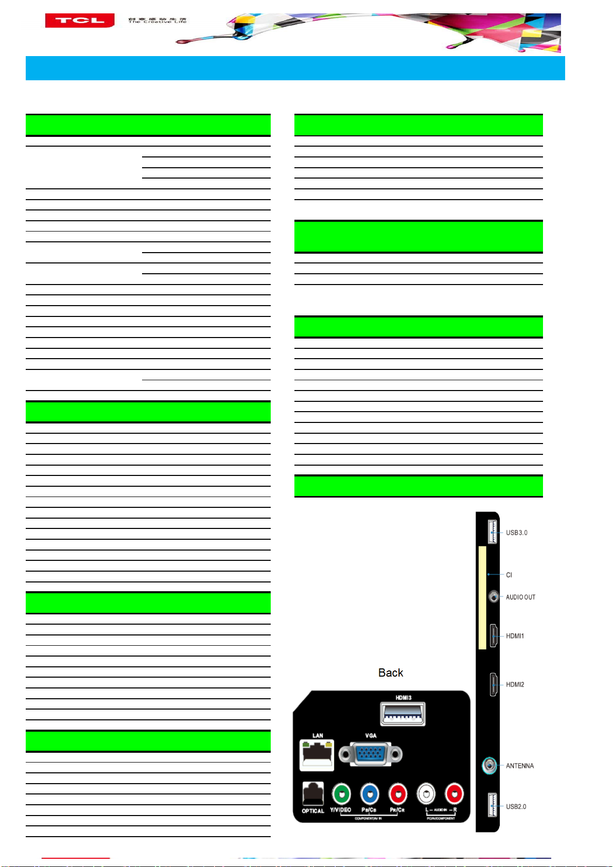
Terminals
Side
Picture
Picture Mode Standard\Dynamic\Natural\Movie\Personal
Screen Mode 16:9\4:3\14:9\Cinerama\Zoom etc.
Noise Reduction Low\Middle\High\Auto\Off
Backlight Adjustable Yes (0~100)
Color Temperature Normal/Warm/Cool/Customer
Gamma Adjustable -4 to 4
Dynamic Contrast Yes
Overscan Yes
Game Mode Yes
Film Mode Yes
Picture Reset Yes
Sound
Speakers Integrated speakers (Bottom side)
Audio Power Output(THD=7%) 2×8W
Auto Volume Control On / Off
Sound Preset Standard\Music\Movie\Clear Voice\Personal
Sound Control
TV Placement
Audio Delay
Sound Bluetooth
Five band equalizer adjust in Personal mode
Desk top / Wall mount
Yes
Yes,for External Bluetooth speaker/soundbar
Back
Page 7
Pre-Installed Application List
YouTube Push Popular VOD posters to Homepage Operation Manual English(Default)
Golive 3.0 Lots of Global Live TV &Movies show Remote Control and batteries RC311 or RC602 (with 2 batteries)
Miracast
App Store 3.3 Special App Store available for download
Browser Webpage Browser
TV Tweets a Social App
Deezer Global Online Music Streaming service
Mediacenter Media/Music play for USB Device
Message Box Messages push
E-Sticker as some function demo in Shop mode
E-Manual Some general basic function introduction
History as some Apps viewing records
nScreen
Wireless Mirroring connecting,to deliver audio
and video content from smartphone to TV
Connect Mobile phone to TV sets and control
the TV like Remote using Phone;
Push media file in Phone to TV Display and
Enjoy big screen picture quality.
Essential Accessories(Default)
Base Stand
AC power cord 1 pcs
RC311
Integrated Packaging
Mechanical ID Picture
Unit:
1246
1464
842.7
16.8
16.8
64.7
20.5
911
247
Mechanical Key Specification
Carton Dimensions LxWxH(mm)
Container Loading---20 feet(pcs)
Container Loading---40 feet(pcs)
Container Loading--40 feet High(pcs)
Net Weight With Stand (Kg) 20.6
Net Weight Without Stand (Kg) 20.3
Gross Weight With Packaging(Kg)
VESA Mounting Dimensions LxH(mm) 300x300
1639*192*1005 Wall Mount
80
172
172
27.6
Optional Accessories
WMB331
Drafted by: ZhangJin Approved by:
Correct specifications/outward depend on the actual model,all specifications are subject to change without prior notice.
Page 8

Factory Test & Alignment Specification For MS68A-AP Series (V1.0).Doc
TCL World-Wide R&D FPD CENTER
Factory Test & Alignment Specification
(FTAS)
for MS68A-AP Series
Version 1.0
PREPARED BY: Li changyong DATE: 2015-10-10
APPROVED BY: DATE:
Page 1 of 9
Page 9
Factory Test & Alignment Specification For MS68A-AP Series (V1.0).Doc
Disclosure
The information contained in this document is proprietary to TCL SZ FPD lab and shall not
be disclosed by the recipient to third persons without the written permission of the team leader
or GM of R&D.
Revision History
Version Issue Date Description of changes
V1.0 2015-10-10 This is the first version.
Page 2 of 9
Page 10
Factory Test & Alignment Specification For MS68A-AP Series (V1.0).Doc
These chassis are designed for LatinAmerica(LA) markets ready for IPTV. The main chip is from
Mstar and supports below features matrix:
Class Item MS68A-LA
Inputs
&
Outputs
Functions
Others
IC Details
&
Position
ATV
( PAL M/PAN N/ NTSC)
DTV
(DVB-T/T2/C)
HDMI
(480i/p, 576i/p, 720p up to 1080i/p, compliant v1.4
with HDCP)
CMP
(YPbPr can support from 480i up to 1080p, audio)
AV
(CVBS, audio)Share with CMP
AV audio out
USB thumb drive
Headphone output
SPDIF output
OAD
WIFI
DIVX
DLNA (DMP)
Internet
3D (auto, top & bottom, side by side, frame
sequencing, …)
1920x2205@24Hz (1920x1080p x2)
1280x1470@50Hz (1280x720p x2)
1280x1470@60Hz (1280x720p x2)
Audio Return Channel (ARC)
I2C connector of MEMC module
Main SW Serial NAND Flash
BIN image
Main IC
Cable & Antenna
Antenna
3
1
1
1
2
- Picture, Video, Audio Playback
- Hub, Mouse, Keyboard rd
0
Spdif
No
Yes
No
Yes
Yes
No
YES
U701
N/A
U501
INFO:
All tests and measurements mentioned hereafter have to be carried out at a normal mains voltage
(100 ~ 240 VAC)
All voltages have to be measured with respect to ground, unless otherwise stated
All final tests have to be done on a complete set including LCD p anel in a room with te mperature of
25+/-7°C
The Picture Performance assessment such as White Balance (luminance and colour temperature)
has to be performed into subdued lighted room after at least 45min of warm-up in order to avoid any
Page 3 of 9
Page 11

Factory Test & Alignment Specification For MS68A-AP Series (V1.0).Doc
temperature drift influence (colorimetry vs time)
1. PCB/SKD Assembly: Test & Alignment
1.1. Pre-Conditions and DC/DC Check
Before power-on, please check the board according to the relevant block diagram and circuit
diagram, and make sure that no serious issue or mistake can destroy the board. For example, the
output of DC/DC and LDO should not be shorted to ground.
Supply a suited voltage and power-on, then check the voltage according to the relevant block
diagram, circuit diagram and voltage spec. The error should less than 5%. For example, the voltage
for main chip (+3V3, AV3.3, +1V2, CORE1V, etc.), the voltage for DDR (DDRV), the voltage for
amplifier (AMP_VCC), etc...
Position Value Remark
UDH1
U101
UD033/UT2
UD015
UDB0
UDN1
5V ±5%
0.95V ±5%
3.3V ±5%
1.5V ±5%
1.0V ±5%
3V3SB ±5%
1.2. SW Image download(Developing
Download the latest release SW from below PDM system:
- Link: http://sw.tcl-cctv.com
- Username: MS68A-LA_Customer
- Password: to be requested!
See Appendix
“How to upgrade FLASH SW using USB”
)
1.3. Project ID Modification
There are different ID stored into the NVM depending on different Panels settings and Models
features, but there’s only one key branching Project ID that includes all. So, it’s not recommended to
modify Panel ID with Hyper terminal as other ID features may not change!
To modify Project ID, you need to go through “Design menuService menuProject ID”, then
spin left or right with RCU “Zoom±” keys to suitable ID (Project name is dynamically refreshed).
See Appendix
Here below is none exhaustive Project ID table for reference:
“How to change Project ID with RCU”
MODEL
ProjectID Panel Name
Page 4 of 9
Page 12

Factory Test & Alignment Specification For MS68A-AP Series (V1.0).Doc
1.4. Functional Test
Once the boards (chassis, KB, IR, PSU…) and the panel are well interconnected, plug all
external generator devices to relevant inputs/outputs below according to their respective test patterns
format and check picture content and sound quality accordingly:
Source Test Signal Test Pattern
2D - Movie 1280x720
Analog/Digital Tuner
(VHF/UHF & CATV)
SPDIF (Coaxial)
AV IN
(CVBS & AUDIO)
CMP
(YPbPr & Audio)
HDMI
(Video & Audio)
RJ45
(LAN)
Headphone via mini jack adapter
Loud Speakers / Enclosures
AV OUT
(Audio)
RF cable generator
Audio Amplifier PCM or Dolby D+
Chroma/Fluke
generator
Chroma/Quantum Data
generator
with beyond HDMI 1.3
and HDCP compliant
DVD/BD player
Internet ICMP packets echo request
RF signal Suitable channel
RF signal Suitable channel
RF signal Suitable channel
2D - Static Picture 1920x1080
1. Frequency Range: full band
2. Standard: NTSC /PAL M
3. DVB-T/T2/C
PAL Half Color & Gray bars
1920x1080i@60Hz
Half Color & Gray bars
2D - Movie 1280x720i@60Hz
3D - Movie 1920x1080@p24Hz
Audio tones can be defined by the factory (i.e. 1 KHz & 3 KHz sweep).
Picture video formats can be changed by the factory according to their own standard.
Remark:1. AV Video & Audio in shared with CMP.
1.5. AD Calibration Test
As SoC is built-in an A/D self-calibration mechanism, ADC need not to be performed any more.
1.6. DDC & EDID & T-Link Test
The E-EDID data structures are according to VESA Enhanced EDID 1.3 (and EIA/CEA-861B for
HDMI). CEA Timing Extension structure has been extended to support all 3D capable timings.
All VGA and HDMI structures have their own BIN profile which are part of main SW and uploaded
at power-on into HDMI switch chipset.
For EDID check, it’s needed to check whether the correct EDID is downloaded by checking
corresponding EDID NVM Checksum or read them out to check bit by bit if it is in line with the
released EDID bin file.
1.7. HDCP Test
Page 5 of 9
Page 13

Factory Test & Alignment Specification For MS68A-AP Series (V1.0).Doc
For HDCP compliancy, it’s needed to check whether the HDCP key has been well set.
1.8. LAN/WLAN Test (MAC address)
MAC Address Upgrade
See Appendix
“How to upgrade MAC Address
2. Product Assembly (PA): Test & Alignment
2.1. Factory Menu
Follow the below steps to pop-up the Factory menu in case of “Factory Key” is disabled:
- Press RCU “MENU” key to display main menu
- Select “Setting” and press “OK” key to enter into setting submenu
- Select “Picture” and press “OK” key to enter into picture submenu
- Scroll down to “Contrast” item
- Press the subsequence RCU keys “9”, “7”, “3” and “5”
In case of “Factory Key” is enabled, just press RCU “Return” key to pop-up again the Factory
menu.
The status of “Factory Key” can be changed in Factory Menu->Hotkey.
Press RCU “OK” key or “RIGHT” key to enter the submenu.
Press RCU “Menu” key to go back to the root menu.
Press RCU “RIGHT” or “LEFT” key to change the values.
Press RCU “OK” key run the function.
Press RCU “Exit” key exit the Factory menu.
See Appendix “Factory Menu Description”
2.2. Warm-up
Following TCL standard and practices, it’s required minimum 15min of Warm-Up that can be
considered as Burn-In.
Additional Aging for White Balance alignment is no more necessary due to consistent Picture
Performance with Cloning usage.
This function is accessible by selecting “Factory menu WARM-UP”, pressing RCU “Zoom+”
key and then leaving Factory menu. Other faster methods are available on above enclosed
SIACP requirements (rev. v3.9).
2.3. White Balance (WB) (Developing)
for Alignment: ± 0.003
for Measurement: ± 0.01
2.4. SHOP-END initial
At final process stage, it’s necessary to perform “Reset shop” before any packing to leave
Page 6 of 9
Page 14

Factory Test & Alignment Specification For MS68A-AP Series (V1.0).Doc
Factory mode and restore User default presets.
This function is accessible by selecting “Factory menu SHOP init”, then pressing RCU “OK”
key. Other faster methods are available on above enclosed SIACP requirements (rev. v3.9).
Appendix “How to upgrade SW EMMC using Mstar tool” (Developing)
Appendix “How to upgrade EMMC SW using USB”
Copy the SW BIN image “MS08upgrade.bin” into USB stick root path.
Note: If there’s already other “
Plug USB stick to the TV USB slot.
Press RCU MENUSetting Software upgradeBy USBConfirm.
Or, turn off the TV press and hold the power key of key boar d before reconnect AC cord to
restart TV for 5-8seconds (Forced Upgrade).
When the "UPGRADING SOFTWARE" picture appears as below, it means TV is uploading
SW BIN image. Waiting a few minutes.
MS08upgrade.bin” into USB root, it needs to be deleted or renamed.
When updating is successful, TV should restart automatically.
Appendix “How to change Project ID with RCU”
Process following subsequence IR codes to change project ID: 062598+MENU+xxx (xxx:
Project ID, ex: 003) with TV automatic restart.
Appendix “How to upgrade MAC Address
Upgrading M AC address need to use the tool in factory and through serial command, the
specific methods according to the operation of the factory guidance.
Appendix “Factory Menu Description”
1- Factory hotkey submenu
Item Sub-item Value Note
Factory
hotkey
Off/On
OFF:hotkey is invalid
ON :hotkey(Return key) is availability
2- Warm-Up Mode submenu
Page 7 of 9
Page 15

Factory Test & Alignment Specification For MS68A-AP Series (V1.0).Doc
Item Sub-item Value Note
Select panel On with left/right key, Press
Warm-UP
Mode
Off/On
“EXIT” key to enter the burning mode;
Press “Menu” key on keyboard to exit the
burning mode
3-ADC submenu
As SoC is built-in an A/D self-calibration mechanism, ADC need not to be performed any more.
4-White Balance submenu
Item Sub-item Value Note
Balance source are:
HDMI, ATV,DTV, PAL, NTSC, CMP
Warm and cool value is relative to Normal
one. Normal is the default Tone mode
R White balance (-127..+128 for gain)
G White balance (-127..+128 for gain)
B White balance (-127..+128 for gain)
R Gray balance (-127..+128 for offset)
G Gray balance (-127..+128 for offset)
B Gray balance (-127..+128 for offset)
Press “OK” key to initial the preset RGB
Gain/Offset value
White
Balance
Source HDMI, etc
Color Temp
Normal
/Warm/Cool
R Gain 000..255
G Gain 000..255
B Gain 000..255
R Offset 000..255
G Offset 000..255
B Offset 000..255
White Balance Init DO
VGA ADC Status NG
YPbPr ADC Status NG
5-Shop init submenu
Item Sub-item Value Note
Shop Init
6-NVM Reset submenu
Item Sub-item Value Note
Reset
ALL
Clear date of NVM in user menu,include
DO
DO
the value related installation,and Clear
date of factory menu except the item of
Balance and sound ,set to default value
Clear NVM values,and set to default
value
Page 8 of 9
Page 16

Factory Test & Alignment Specification For MS68A-AP Series (V1.0).Doc
7-Power On Mode submenu
Item Sub-item Value Note
Power
On Mode
8-USB UPDATE submenu
Item Sub-item Value Note
Main Upgrade
MEMC Upgrade
HDCP Uprade
USB
UPDATE
Mboot upgrade
NVM Upgrade
NVM backup
CH list Upgrade
CH list backup
ON/LAST/STB
ON: The set will power on after switching
on power
STB: Force TV to start in standby
Last: Force TV to start from last power
status
Upgrade software
Upgrade MEMC
Upgrade HDCP
Upgrade Mboot
Upgrade NVM
Backup NVM
Upgrade CH list
Backup CH list
9-Device ID test submenu
Item Sub-item Value Note
Select to choose the things you want to
clone
Press “Right” key to copy the data(WB,
ADC, picture setting, etc) to USB
Press “Right” key to set the data(WB,
ADC, picture setting) from USB
USB
Clone
USB Clone Mode
Channel List
User Setting
TV TO USB DO
USB TO TV DO
All
EEPROM
Appendix “Instructions of Updating SW”
1. The following IC should be pre-copied before SMT process(UF02/UF03/U107 only for
MSO8UF4-LA).
Pos
ition
U701 IC-
PART TYPE Part Number SW
13-THA19N-8GB (CPP) Mboot, Main Software
THGBMBG6D1KBAIL
A19NM 8GB E-MMC
VER5 0_E_REV1
0_131219
2. The MAC Address, HDCP KEY, Device ID must be upgrade by debug port into U701.
Page 9 of 9
Page 17

I²C Bus Block Diagram
For Panel
FFC
HDMI1
HDMI2
HDMI3
HDMI1_SCL
HDMI1_SDA
HDMI2_SCL
HDMI2_SDA
HDMI3_SCL
HDMI3_SDA
SYS_SCL
MS6488
SYS_SDA
TAS_SCL
TAS_SDA
TUNER_SCL
TUNER_SDA
DEMO
(UM3_7811)
U101
(5V to core)
AMP
(UA01)
Tuner
(TUN1)
9
Page 18

5
4
3
2
1
MS6488 system diagram
D D
U601 4G
LIF_N
MXL661
UT1
U301
5V USB_5V
EN
RT9711A
5V
HDMI2
ARC
HPD
DDC_SCL
DDC_SDA
RX[0..8]
+5V
GND
CEC
P402
LIF_P
AGC2
SDA
SCL
GND
3.3V
HDMI1
HPD
DDC_SCL
DDC_SDA
RX[0..8]
VBUS
CEC
CD_SENSE
GND
USB_RXP
USB_RXN
USB_TXP
USB_TXN
P401
+5V
DP
DM
GND
+5V
DP
DM
GND
DP
DP
GND +5V
DMDM
DM
TIFP
P307
P307
1
2
3
4
DEBUG
DEBUG
SIFIP
SIFIN
SIFQP
SIFQN
TS OUT
AGC2
SDA
SCL
ATBM7812B
HDMI1_DET
UART-RX
UART-TX
HDMI3_DET
TIFN
GND
3.3V
TO SOC TS1 IN
5V
HDMI2_DET
HDMI3
U401
G524
DDC_SCL
DDC_SDA
RX[0..8]
+5V
CEC
GND
5VVBUS
EN
HPD
P403
DVBS_IP
DVBS_IN
DVBS_QP
DVBS_QN
AGC
SDA
SCL
GND
5V
SHARP TUNER
C C
CI_DATA
CI_ADRESS
CI_CLK
CI_COMMAND
SDA
SCL
PCMCIA
GND
5V
VGA IN
VGA IN
SPDIF OUT
SPDIF_OUT
RCA&OPTICAL
B B
YPBPR/AV IN
Y
PB
PR
AUDIO_L
AUDIO_R
EARPHONE OUT
EARPHONE_OUT
C385
RJ45RJ45
P901
TD+
7
NC
TD-
TDCT
8
CH_GND
RDCT
13
GND1
14
RD+
GND2
RD-
C387
C387
1nF/2KV/1206
A A
1nF/2KV/1206
C385
1nF/2KV
1nF/2KV
1
2
4
7575
5
3
6
7575
16
TX+
14
TX-
15
7575
TCM
11
RX+
9
RX-
10
7575
TCM-
HST-0041
HST-0041
U901
U901
TD+
RD+
SMDTR16P
SMDTR16P
TD-
RD-
AV OUT
1
3
6
8
3V3SB
3V3SB
AV1_V
AV1_L
AV1_R
RESET
RESET
WIFI
USB2.0
USB3.0
VIFN
VIFP
IF_AGC
TU_SDA
TU_SCL
DP0
DM0
DP1
DM1
DP3
DM3
USB_RXP
USB_RXN
USB_TXP
USB_TXN
HDMI_CEC
HDMI1_HPD
HDMI0_SCL
HDMI0_SDA
HDMI0_RX[0..8]
HDMI_ARC
HDMI1_HPD
HDMI1_SCL
HDMI1_SDA
HDMI1_RX[0..8]
HDMI2_HPD
HDMI2_SCL
HDMI2_SDA
HDMI2_RX[0..8]
AVOUT_V
AVOUT_L
AVOUT_R
SPDIF
MIC_IN
PHY_TP
PHY_TN
PHY_RP
PHY_RN
MCU_RESET
U501
MS6488
A_RAMADR[0..13]
A_RAMBAK[0..2]
A_RAMCTL[0..13]
A_RAMDAT[0..15]
A_RAMDAT[16:31]
B_RAMADR[0..13]
B_RAMBAK[0..2]
B_RAMCTL[0..13]
B_RAMDAT[0..15]
B_RAMDAT[16:31]
EMMC_CLK
EMMC_CMD
EMMC_D[0:7]
EMMC_RESET
TAS_SDA
TAS_SCL
CAMADR[0-14]
CAMDAT[0-7]
CAMCTL[0-9]
TS0 IN[0-10]
TS1 IN/ OUT[0-10]
PWR-ON/OFF
GPIO_PM
SYS_SDA
SYS_SCL
I2S_OUT[0..3]
VB1[0:7]
OSD_VB1[0:3]
1V2_VDD
CORE_POWER
1V5_DDR
33VSTB
1V2_VDDC
CORE_POWER
1V8
1V8
1V5_DDR
3V3
3V3
3V3SB
RAMADR[0..14]
RAMBAK[0..2]
RAMCTL[0..13]
RAMDAT[0..15]
U602 4G
RAMDAT[16..31]
RAMCTL[0..13]
RAMBAK[0..2]
RAMADR[0..14]
U603 2G
RAMADR[0..14]
RAMBAK[0..2]
RAMCTL[0..13]
RAMDAT[0..15]
U604 2G
RAMDAT[16..31]
RAMCTL[0..13]
RAMBAK[0..2]
RAMADR[0..14]
U701
EMMC_CLK
EMMC_CMD
EMMC_D[0:7]
EMMC_RESET
U700
NAND_CLK
NAND_CMD
NAND_D[0:7]
NAND_RBZ
CAMADR[0..14]
CAMDAT[0..7]
CAMCTL[0..9]
TS_OUT[0..10]
TS_IN[0..10]
PANEL_ON
EMMC 16GB
NAND 4Gb
CAM
UA01
PDN#
RESET#
SDA
SCL
I2S[0..3]
12V
SYS_SDA
SYS_SCL
1.5V
GND
1.5V
GND
1.5V
GND
1.5V
GND
1V8
3V3
GND
1V8
3V3
GND
+5V
GND
VS
AMP 5707
OUT_L+
OUT_L-
OUT_R+
OUT_R-
GND
+3.3V
24V
LVDSPW_ON
PANEL_VCC
12V
MOS SWITCH
1V8
3V3
1V5_DDR
1V5_DDR
3V3
AMP_VCC
P1001/P1002
VB1[0:7]
OSD_VB1[0:3]
12V
SDA
SCL
GND
5
4
3
2
1
Page 19

5
4
3
2
1
MS6488 Power diagram
D D
12V_M
12V
C C
B B
L100L100
L104L104
130mA
UDN1
DC_IN DC_OUT
420mA
MAX 1.2A
SY8291
L101L101
1600mA
24V/12V
UA01
AMP 5707
A A
UDH1
最大负载情况:
MHL
充电,同时播放
USB
时达到最大值
3.3VSB
1500mA
430mA
200mA
2200mA
POWER_ON
390mA
20mA
10mA
MOS
3V3
3V3
3.3VSB
3.3VSB
3.3VSB
4410mA
DC_IN DC_OUT
EN
UDB0
MP8765
DC_IN DC_OUT
EN
U101
MSH6110A
DC_OUT
DC_IN
EN
U102
TPS54531
SOC
IR
KEY
;
1V2_VDDC
MAX 5A
CORE_POWER
5V
4830mA
MAX 5A
R141 0RR141 0R
D105D105
D104D104
R1420RR142
0R
330mA
1400mA
180mA
240mA
480mA
DC_IN DC_OUT
UD015
SY8034
DC_OUT
DC_IN
UD033
AS1117-3.3
5V_IN 5V_OUT
U401
5V_IN 5V_OUT
U300
DC_IN DC_OUT
UT2
DC_IN DC_OUT
U202
1440mA
MAX 3A
3.3V
330mA
G524B
RT9711A
AS1117-3.3
MAX 1A
RT8096A
1500mA
4300mA
2000mA
1V5_DDR
290mA
OUT
IN
40mA
BT8551
2000mA2000mA
1400mA
TUNER_3.3V
180mA
MAX 760mA
AV 400mA
200mA
1.8V
12V
1V2_VDDC
CORE_POWER
1.5V
2Gb*2+4Gb*2
1.5V
SOC
+3.3V
SOC
+3.3V
AMP 5707
+3.3V
EMMC
VDD-EMMC
VDD-EMMC
VBUS
USB_5V
USB2.0/3.1
TUNER_3.3V
1V1
VBUS
PANEL
SOC
SOC
DDR3
EMMC
SOC
MHL
TUNER
DEMO
WIFI
5
4
3
2
1
Page 20

12 11 10 9 8 7 6 5 4 3 2 1
H
H
5V TO DDR 1V5
R136
NC/
Only for 12V(14PIN)
(5)
3V3SB
GND
3V3SB
R134
10K
R135
10K
NC/
R104
2K2
GND
R102
220R
1000P
DIMING_DET
C108
3V3SB
H 100% ADIMING_MAX(SEPARATED 3D_CTRL AND ADIM)
5V
POWER_ON
L 50% ADIMING_MAX(3D_CTRL AND ADIM SHARE PIN)
(5)
WHEN NO FASTBOOT :R137 MOUNT,R136,D102,D103 NC
WHEN NEED FASTBOOT:R137,R136 NC,D102,D103 MOUNT
WHEN NEED FASTBOOT,NO NEED STANDBY POWER:R136 MOUNT,R137,D102,D103 NC
POWER BD CONNECTOR
12V-1
T
3D_CTRL
T
A-DIM
R154
220R
POWER_ON
R153
220R
R105
220R
T
C146
0.01U
T
GND
PW-ON
C147
0.01U
C100
1000P
T
GND
GND
3D_CTRL
(5)
G
R103
10K
3D_CTRL
12V
GND
A_DIM
POWER_ON
12V
12V
12V12V
GND
3.3VSB
GND
DIM_PWMBL_ON
Must controlled by PWM
A_DIMING
(5)
GND
R152
10K
BL_ON_OUT
(5)
GND
GND
R101
10K
P102
2 1
4
6
8
10
12
14
12V
T
12V-2
16V
NC/
C116
C149
0.1U
PWM-DIM
0.01U
GND12BL-ON
L102
T
C145
0.01U
GND
T
120R
NC/
C126
3
5
7
9
11
13
470U
GND
T
T
STB-3V3-1
STB-3V3
GND
P_DIMING
L101
L100
L104
R157
220R
220R
220R
220R
3V3SB
DIM_OUT
R156
10K
GND
AMP_VCC
12V_M
(5)
POWER_ON_OUT
0R
D102
CMS06
D103
CMS06
R137
0R
NC/
(Vin=2.7V-6V)
CDE1
10U
GND
CDE2
0.1U
GND
GND
Vref=0.6V
RDE2
91K
RDE3
3K6
UD015
1
FB
2
PG
3
IN
4
PGND
AN_SY8034
RDE1
100K
8
SGND
7
GND
EN
6
LX
5
NC
(0.85MHz<Fosc<1.15MHz)
R131
3K3
LDE1
2.2UH
NC/
FAST_BOOST
CDE6
22P
RDE4
150K
(5)
Vout=1.55V
1V5_DDR
T
CDE3
CDE4
22U
22U
GND
CDE5
0.1U
1V5_DDR
@max3A
G
F
RDB6
2K4
GND
RDB9
NC/
CDB2
0.1U
GND
47K
RDB0
100K
NC/
15
12V TO 5V
12V_M
E
(Vin=4.5V-18V,PS=1mW)
CDH1
CDH2
10U
10U
GND
CDH3
0.1U
POWER_ON
DH1
BAS316
GND
RDH1
120K
RDH2
22K
1.86V
CDHD
1U
GND
UDH1 TPS56528
1
2
3
4
CDH5
2U2
EN
VFB
VREG5
PG
Fsw=650KHz
VIN
VBST
SW
GND
12V_M
8
CDH4
0.1U
7
6
5
GND
GND
CDHA
NC/
RDH7
NC/
LDH1
4.7UH
220P
6R8
RDH4
33K
Vref=0.6V
RDH5
3K6
RDH6
820R
CDH6
NC/
47P
CDHB
CDHC
10U10U
Vo=0.6-7V
CDH7
10U
GND
CDH8
10U
5A max
CDH9
0.1U
5V
3V3
R120
3K3
(Vin=5V-22V)
CDB0
10U
CDBC
GND
0.1U
CDB1
10U
1
2
VIN
SW3
PGND
RDB1
36K
14
3
12V TO 1V2_VDDC
13
AGND
NC1
4
12
FB
EN
UDB0
MP8765
NC2
PG
5
RDBA
NC/
0R
Vref=0.6V
GND
CDB4
1U
11
10
VCC
MODE
7
6
GND
BST
SW2
SW4
SW1
VOUT
CDB3
0.1U
VID
CDB5
0.22U
9
16
8
RDB5
4R7
RDB2
22K
NC/
CDBB
220P
RDB7
NC/
10R
GND
Fixed Fsw=500KHZ
Fixed OCP=8.5A
RDB4
1M
LDB0
1UH
RDB3
470R
CDB6
220P
CDB7
22U
CDB8
22U
CDB9
GND
VID
1V2_VDDC
T
CDBD
22U
22U
max5A
CDBA
0.1U
R124
220K
0R
R125
1V2_VDDC
NC/
GPIO_VID_0
1V2_VDDC
GND
Q102
2N7002K
R130
L
0.95V
4K7
R129
4K7
3V3SB
GPIO_VID_0
H
1V
(5)
F
E
GND
D
D
(Vin=4.5V-17V)
12V_M
NC/
R132
100K
C118 0.47U
GND
C107
10U
C117
10U
GND
C115
0.1U
C119
1U
C
Core Power
(Vin=5V-40V)
12V_M
B
CDN1
GND
2.2U
CDN2
2.2U
CDN3
0.1U
RDN5
270K
RDN6
82K
SYS_SDA_1
(5)
6
LX
5
IN
4
EN
AN_SY8291
FSW=800KHz
R106
3K3
R133
10K
UDN1
BS
GND
FB
3V3
3V3
1
2
3
1
2
3
4
GND
EN
FB
VREG5
SDA
U101
MSH6110A
CDN4
0.1U
0.6V
RDN2
5K6
PVDD
BSR
SW
SCL
R161
4K7
4K7
R162
GND
8
7
6
SYS_SCL_1
5
LDN1
4.7UH
DN1
SR34
C120
SYS_SCL
SYS_SDA
0.1U
(5)
RDN1
27K
R163
0R
0R
R164
1000P
RDN4
10K
L106
2.2UH
SYS_SCL_1
SYS_SDA_1
CDN9
GND
CDN5
22U
GND
CDN6
22U
C125
330P
3V3SB
T
GND
3V3SB
CDN7
0.1U
R122
18K
GND
max:1.2A
C121
22U
CORE_POWER
C122
C123
22U
22U
T
0.95V
C124
0.1U
CORE_POWER
5V
C105
UD033
AS1117-3.3
10U
C101
0.1U
GND
VIN
IR/KEY/SPEARKER
4
4
GND/ADJ
OUT
2
3
3V3
1
T
3V3
C104
10U
P104
NC/
1
2
3
4
5
3V3SB_1
6
7
8
9
10
IR_1
LED_1
KEY_1
R+
R-
L-
L+
GND
GND
1
2
3
4
5
6
7
8
9
10
P103
R+
R-
LL+
3V3SB_1
IR_1
LED_1
KEY_1
C110
330P
GND
IR_3V3SB
GND
GND
C111
330P
IR
T T
C112
0.01U
KEYLED
T T
3V3SB
R118
4K7
R115
10K
L103
220R
R116
470R
R117
1K
3V3SB
IR_IN
LED_OUT
(5)
(5)
D101
NC/PESD5V0S1BL
12
R119
22K
C114
0.1U
GND
GND
KEY_IN
C
(5)
GND
A
THIS DRAWING CANNOT BE COMMUNICATED TO UNAUTHORIZED PERSONS COPIED UNLES S PERMITTED IN WRITING
GND
RDN3
330R
Index-Lab
Last saved :
SBU :
TCLNO:
NAME Last modifDESCRIPTIONDATE
.............
DESIGNATION
DESIGNATION
ON:
BY:
DRAWN
TCL Thomson Electronics Singapore Pte. Ltd.
8 Jurong Hall Road #28-01/06
The JTC Summit SINGAPORE 609434
Tel (65) 63092900 Fax (65) 63092999
CHECKED
PAGE:
ON:
BY:
OF :
A
123456789101112
FORMAT DIN A1
Page 21

12 11 10 9 8 7 6 5 4 3 2 1
H
MAXLINER TUNER MXL661 ON BOARD
H
TU_3V3
TU_3V3
VDD_1V8
Read Add:97D
Write Add:96D
GND
TU_3V3
TUN1
0R
NC
LT2
CT2
NC
5P6
CT2
5P6
33NH
LT2
NC
33NH
LT5
NC
33NH
VDD_1V8
LT5
33NH
GND
LT3
0R
8.2NH
CT1
120P
GND
LT7
0.22UH
NC/
CT3
150P
NC/
GND1
GND2
GND3
GND4
GND5
GND6
1
S1
2
FT1
3
4
5
6
7
GND
GND
LT1
0.33UH
GND
3
1 2
DT1
0BAV99
G
DVB-T/T2
LT3
8.2NH
balun
unbalun
L204
75R
NC
R243
NC
0R
R244
GND
CT6
CT4 1000P
CT5 1000P
LT6
1000R
CT12
0.1U
GND
0.1U
AGC_1
GND
RT7
100R
1
2
3
4
5
6
CT7
0.1U
RT3
100K
CT13 1U
661_AS
VDD_3P3A
LNA_INP
LNA_INN
VDD_1P8A
AGC_2/GPO_3
AGC_1
241423
AS
IF_OUTP_2/GPO_1
7
F
CT14
0.01U
22
21
RESET_N
VDD_1P8C
GND_XTAL
UT1
MXL661
IF_OUTN_2/GPO_2
IF_OUTP_1
IF_OUTN_1
9
8
10
CT10
CT11
XT16M
16M
GND
19
20
XTAL_N
XTAL_P
CLK_OUT
VDD_IO
GND_DIG
VDD_1P2
VDD_1P8B
VDD_3P3B
11
12
TU_3V3
GND
0.1U
0.1U
18
17
SDA
16
SCL
15
13
CT19
0.1U
TUNER_FAT+
TUNER_FAT-
VDD_1V8
CT17
1U
661_AS
GND
CT15
1800P
GND
TU_3V3
CT16
0.1U
RT8
RT9
TUNER_AS=0XC6
R229
0R
TUNER_AS=0XC0
R230
0R
GND
CT33
22P
GND
100R
100R
DVB-S/S2 Project use 0xC6
Other project use 0xC0
RT16
RT15 33R
CT34
22P
GND
Close to SOC
GND
33R
NC/
CT28
22P
CM31
TU_3V3
RT10
4K7
0.1U
Close to SOC
Or connect to the nearest 3V3
RT11
4K7
TU_IF+_IN
TUNER_SDA
TUNER_SCL
(5)
(5)
(5)
3V3_DEMO
1V1
495mA
GND
GND
CM13
22U
CM20
CM14
10U
CM21
2U210U
CM15
2U2
CM22
0.1U
CM16
0.1U
CM23
0.1U
CM17
0.1U
CM25
CM24
0.1U
0.1U
CM18 CM19
0.1U
3V3_DEMO
0.1U
G
1V1
F
(5)
(5)
(5)
(5)
(5)
(5)
(5)
(5)
(5)
5V
12V_M
(Vin=2.7V-7)
C204
10U
GND
C213
220U
35V
GND
C205
0.1U
C211
10U
C232
100U
16V
5V TO DEMO 1V1
R201
100K
GND
4
5
Vref=0.6V
R202
100K
R203
15K
VIN
FB
U202
RT8096A
LX
GND
EN
3
2
1
GND
L201
2.2UH
C206
22P
R205
100K
C207
22U
12V TO TUNER LNB
R245
0R
C215
GND
R210
10K
0.1U
Close to TUNER
DISEQC_OUT
R211
100R
R247
100R
GND
C216
0.1U
D201
MBRX14
L202
10UH
GND
D203
MBRX14
C224
4U7
GND
D202
MBRX14
C217
0.1U
U203
1
LNB
2
BOOST
3
LX
4
VIN
RT5047
TONE
NC
SEL
EN
8
7
6
5
C208
22U
C214
0.22U
F_SEL
LNB_EN
1V1_DEMO
T
C209
0.1U
GND
TUNER_LNB
C210
0.01U
GND
H :18.3V
L :13.3V
H :Power on
L :Power off
1V1
@max1A
5V TO TUNER 3V3
4
4
VIN
3
CT42
0.1U
OUT
2
GND/ADJ
1
GND
GND
CT43
10U
R236
0R
R237
0R
3V3_DEMO
T
UT2
AS1117-3.3
5V
CT41
10U
GNDGND
TU_3V3
3V3_DEMO
E
D
C
CT8
22P
3V3
Close to SOC
Close demod
RM5
D_IF_AGC
E
10K
CM3
0.1U
GND
RM22
1K
Close tuner
CM1
0.1U
GND
IF_AGC_T2
12V_M
AGC_SW
(5)
10K
10K
R207
R208
R248
0R
Q201
2N7002K
C
B
E
GND
NC/
Q202
BT3904
GND
R206
10K
CT21
0.022U
RT12
0R
TU_IFAGC_OUT
(5)
GND
CT9
22P
CM33
0.1U
CT29
NC/
22P
GND
RT18/RT19/RT20 decided by the SOC
TU_IF-_IN
D
DEMO ATBM7812B FOR T2,S2
24M
Read Add:0X81H
X24M1
GND
I2C_ADDR
35
32
34
36
GND1
33
AVDD33
CAVDD
ADDR
31
XTALO
UM3
ATBM7812B
SDAM
SCLM
CVDD1
GPO5
GPO4
123456789
SDA_DVBS
SCL_DVBS
LNB_EN
F_SEL
1V1
GND
DISEQC_OUT
DISEQC_IN
S2_AGC
28
29
30
GP01
DISEQC_OUT
DISEQC_IN
XTALI
VDD33A
STATUS
TSSYNC
TSVLD
3V3_DEMO
TSSYNC
TSVLD
RM6
2K7
GND
CM29
33P
3V3_DEMO
1V1
GND
25
261127
CVDD4
TEST_MODE
VDD33C
SDAS
SCLS
CVDD3
RESET
CVDD2
VDD33B
TSCLK
TS0
TS1
10
12
D_TSDATA1
D_TSDATA0
TSCLK
TS7
TS6
TS5
TS4
TS3
TS2
24
23
22
21
20
19
18
17
16
15
14
13
1V1
3V3_DEMO
D_TSDATA7
D_TSDATA6
D_TSDATA5
D_TSDATA4
D_TSDATA3
D_TSDATA2
TSCLK
TSVLD
TSSYNC
RM7
22R
RM8
22R
RM9
22R
NC/
CM26
10P
GND
37
38
39
40
41
42
43
44
45
46
47
48
CM30
33P
SIFIP
SIFIN
SIFQP
SIFQN
RSSI
CLK_IO
TIFP
TIFN
VDD33D
CVDD5
GPO2
GPO3
Write Add:0X80H
1V1
3V3_DEMO
R233
0R
CM8
2U2
C
SHARP TUNER FOR S2
TUNER_FAT+
TUNER_FAT-
C220
0.022U
TT
TT
TU_3V3
T
T
TT
C225
10P
D204
1SMC20AT3G
R225
100R
R226
100R
R227
100R
R228
100R
TUNER_LNB
TU_3V3
MODULE_AGC
C202
C203
C226
10P
0.1UC200
0.1UC201
0.1U
0.1U
TU_3V3
SIF_IP
SIF_IN
SIF_QN
SIF_QP
NC/
NC/
R224
100R
R223
100R
R209
100R
R212
100R
3V3_DEMO
R213
4K7
TUNER_SDA
TUNER_SCL
R214
4K7
SDA_DVBS
SCL_DVBS
(5)
(5)
3V3_DEMO
S/S2-DEMOD_AS=0X98
R204
4K7
I2C_ADDR
DEMOD_AS=0X80
R246
4K7
GND
TUN2
LNB
T
1
B1
2
B2
SAGC
3
AGC
B
QN
QP
SDA
SCL
CLK_OUT
SHARP TUNER
DVB-S/S2
IP
4
IP
IN
5
IN
QN
6
QP
7
SSDA
8
SSCL
9
10
R232
0R
GND
CM4
0.01U
GND
CM6
1U
CM32
NC/
47P
GND
DVB-S/S2 Project use 0x98
Other project use 0x80
GND
CM34
NC/
CM9
2U2
SIF_IP
SIF_IN
SIF_QP
SIF_QN
47P
3V3_DEMO
1V1
IRQ
D_IF_AGC
CM11
10P
CM27
NC/
3V3_DEMO
RM3
47K
CM7
1U
GND
GNDGND
CI_MCLKI
CI_MIVAL
CI_MISTRT
CM28
NC/
10P
GND
T2_RST
RM20 100R
RM19 100R
CM10
10P
10P
(5)
(5)
(5)
(5)
TUNER_SDA
TUNER_SCL
D_TSDATA7
D_TSDATA6
D_TSDATA5
D_TSDATA4
D_TSDATA3
D_TSDATA2
D_TSDATA1
D_TSDATA0
(5)
(5)
RM10
22R
RM11
22R
RM12
22R
RM13
22R
RM14
22R
RM15
22R
RM16
22R
RM17
22R
CI_MDI7
CI_MDI6
CI_MDI5
CI_MDI4
CI_MDI3
CI_MDI2
CI_MDI1
CI_MDI0
TU_3V3
MODULE_AGC
C212
C227
C228
A
10U
close TUN2
0.047U
GND
1000P
0.01U
C218
1K
0.01U
C219
R216R215
10K
THIS DRAWING CANNOT BE COMMUNICATED TO UNAUTHORIZED PERSONS COPIED UNLES S PERMITTED IN WRITING
S2_AGC
Index-Lab
Last saved :
SBU :
TCLNO:
NAME Last modifDESCRIPTIONDATE
.............
DESIGNATION
DESIGNATION
ON:
BY:
DRAWN
TCL Thomson Electronics Singapore Pte. Ltd.
8 Jurong Hall Road #28-01/06
The JTC Summit SINGAPORE 609434
Tel (65) 63092900 Fax (65) 63092999
CHECKED
PAGE:
ON:
BY:
OF :
A
123456789101112
FORMAT DIN A1
Page 22

12 11 10 9 8 7 6 5 4 3 2 1
USB2.0+ RS232
UART_TX
UART_RX
T
U_RX
U2_D-
U2_D+
U_TX
T
GND
GND
USB5V
T
P304
9
1
8
2
7
3
6
4
5
10
11
MNT-HOLE1
MNT-HOLE2
USB3.0
T
USB_5V
U_TXP
U_TXN
U4_DU4_D+
U_RXP
U_RXN
GND10
T
GND
9
1
8
2
7
3
6
4
5
10
11
P303
NC/
MNT-HOLE1
MNT-HOLE2
U2_D-
3P3
C313
GND
U2_D+
C314
3P3
C317
GND
3P3
U4_D+
C318
3P3
U4_D-
U_RX
U_TX
U2_D-
U2_D+
NC/
D304
PESD5V0U1UL
NC/
D305
PESD5V0U1UL
NC/
D300
PESD5V0U1UL
NC/
D301
PESD5V0U1UL
U_TXN
U4_D-
U_RXN
P310
1
VCC-1
2
DNEG-1
3
DPOS-1
4
GND-1
5
6
MNT-HOLE1
MNT-HOLE2
GND
USB_5V
U2_DU2_D+
GND
WHEN VGA MOUNT,P310 MOUNT,P304 NC
WHEN NO VGA :P310 NC,P304 MOUNT
NC/
U301
1
GND
2
3
4
5
11
I/O1
VDD
NC1
I/O2
I/O3
ISLAND
AZ1065-06F
I/06
GND
NC2
I/O5
I/O4
U_TXP
10
9
8
GND
7
6
U4_D+
U_RXP
AV OUT
1
2
3
SCT1_AUL_OUT
4
5
AUDIO_L_OUT
NC/
D310
AUDIO_R_OUT
NC/
D311
SCT1_V_OUT
SCT1_AUR_OUT
GND
T
12
C330
470P
PESD5V0S1BL
T
C331
470P
PESD5V0S1BL
2 1
CVBS
P305
GND
SCT1_AUL_OUT
SCT1_AUR_OUT
R
L
CVBS_OUT
AUDIO OUT
R301
470R
GND
R300
470R
T
R391
0R
1UC312
C311 1U
AVOUT1_L_OUT
C351
120P
GND
AVOUT1_R_OUT
C352
120P
GND
R326
AVOUT1_V_OUT
0R
R327
75R
GND
(5)
C351,C352 CLOSE SOC
(5)
H
(5)
G
F
H
HD_Y
T
T
HD_PB
T
T
HD_L
T
HD_PB_IN
HD_PR
GND5
P300
GREEN
BLUE
RED
WHITE
G
RED
D308
GND GND
NC/
HD_Y_IN
PESD5V0U1UL
10
9
8
7
6
5
4
3
2
1
HD_PB_IN
D307
T
T
HD_R_IN
GND
NC/
PESD5V0U1UL
NC/
HD_PR_IN
D306
GND
GND
HD_L_IN
GND3
HD_R
PESD5V0U1UL
F
YPBPR
HD_Y_IN
C319
R305
NC/
GND
NC/
C321
NC/
C320
22P
12K
12K
22P
22P
R309R302
HD_PR_IN
GND
GND
GND
R307
10K
R308
10K
75R
R304
75R
R303
75R
C326
560P
C324
560P
GND
33R
33R
R311
33R
C306
1U
C307
1U
R306
R310
CLOSE TO IC
C322
0.047U
C325
0.047U
C323
0.047U
HD_L
HD_R
HD_Y
HD_PB
HD_PR
(5)
(5)
(5)
(5)
(5)
0.1U
C305
C333
0.1U
GND
GND
C332
220U
16V
16V
470U
C304
close to p303
USB_5V
close to p304
USB_5V
(5)
(5)
(5)
(5)
(5)
(5)
(5)
(5)
(5)
(5)
UART_RX
USB2_D-
USB2_D+
UART_TX
USB_TXP
USB_5V
USB_TXN
USB4_D-
USB4_D+
USB_RXP
USB_RXN
U4_D-
U4_D+
R333
NC/
470R
470R
NC/
R334
C316 0.1U
C315
R335
R336
R338
R337
NC/
PESD5V0U1UL
NC/
PESD5V0U1UL
2R2
2R2
2R2
2R2
0.1U
D302
D303
R341
2R2
2R2
R342
U2_D-
T
U2_D+
T
USB4+
USB4-
T
USB_5V
T
GND6
T
GND
U300
5V
C300
VGA IN
P311
16
E
D
5
15
10
4
14
9
3
13
8
2
12
7
1
11
6
17
VGA_SCL
VGA_RXD
VGA_VS
VGA_BLU
VGA_HS
VGA_GRN
VGA_SDA
VGA_RED
VGA_TXD
GND
VGA_SCL
T
VGA_RXD
T
VGA_VS
T T T T
VGA_B
VGA_HS
VGA_G
VGA_SDA
T T
VGA_R
VGA_TXD
T
GND
GND GND
GND
GND
R378
75R
R379
75R
R380
75R
VGA_RED
VGA_GRN
VGA_BLU
VGA_HS
R382
2K2
VGA_VS
R384
2K2
GND
R374
33R
33R
R376
33R
100R
100R
R375
68R
R377
R381
R383
C380
C381
C382
C383
RIN0
0.047U
GIN0
0.047U
GIN0N
0.047U
0.047U
VGA_HSYNC
VGA_VSYNC
BIN0
VGA_SCL
VGA_SDA
VGA_RXD
VGA_TXD
3V3SB
R385
4K7
R386
4K7
R387
100R
R388
100R
R389
100R
100R
R390
UART_RX
UART_TX
(5)
(5)
(5)
USB3_EN
10U
R332
100R
GND
GND
5
VIN
R340
NC/
10K
4 3
EN/EN# NC
R339
22K
RT9711A
EARPHONE_L
(5)
SPDIF
C
(5)
SPDIF_OUT
SPDIF_OUT
Optical
0R
R344C329
33R 47P NC
C327 R343 C328 P302 P306
0.1U NC
P306
CLOSE TO SOC
C329
0.1U
R344
220R
C327
220P
GND
R343
120R
COAXIAL
SPDIF
T
C328
0.1U
3V3
SPDIF_GND
SPDIF
SPDIF_VCC
T
T
GND
P302
2
IC
DRIVE
P306
BLACK
TX
LED
1
VIN
3
VCC
2
GND
1
SPDIF
NC/
D309
GND
12
(5)
PESD5V0S1BL
1
VOUT
2
GND
EARPHONE_R
GND
C301
10U
R353
1K
NC/
R360
1K
NC/
USB_5V
C363
47P
NC/
GND
C368
47P
NC/
GND
C362
1U
NC/
C367
1U
NC/
R352
33K
NC/
33K
R359
NC/
C361
GND
GND
EARPHONE_L
EARPHONE_R
R350
33K
NC/
R351
1K
NC/
1500P
NC/
R358
1K
NC/
R357
33K
NC/
C366
1500P
NC/
C302
C303
AMP_RESET
C360
150P
NC/
U302
DRV632
NC/
C365
150P
NC/
22U
22U
1
14
10K
NC/
+INR
+INL
GND
HP_L
HP_R
R349
2
-INR
-INL
13
C364
1000P
NC/
headphone out
HP_L
GND
5
10
GND
6
MUTE
PGND
9
R356
10K
NC/
C359
1U
NC/
7
PVSS
PVDD
8
NC/
NC/
CN
CP
3V3
R354
3K3
R355
3K3
C358
1U
NC/
GND
C357
0.1U
NC/
3V3
GND
C356
100U
NC/
3
OUTR
OUTL
12
GND
4
SGND
UVP
11
16V
HP_R
PLug Off: H
Plug on: L
HP_DET
(5)
close to SOC
R330
4R7
R331
4R7
Note:
GND
C349
0.1U
R348
1KR345
1K
GND
3V3SB
C353
0.1U
R347
1K
R346
10K
GND
L301
C3350
0.1U
10UH
10UHL303
GND
2200P
GND
L302
C355C354
2200P
L304
1000R
1000R
HP_R
T
HP_DET
T
HP_L
T
GND
GND
T
5
4
3
2
1
AV/Y
PR/L
PB/R
GND
E
D
C
P301
Coaxial
0.1U
220R
220P
120R
NC
P302 NC
B
VGA_SCL
NC/
VGA_SDA
12
NC/
VGA_HS
NC/
A
D326
PESD5V0S1BL
2 1
D325
D324
PESD5V0S1BL
2 1
VGA_VS
12
NC/
D323
PESD5V0S1BL
PESD5V0S1BL
VGA_RED
12
NC/
D322
THIS DRAWING CANNOT BE COMMUNICATED TO UNAUTHORIZED PERSONS COPIED UNLES S PERMITTED IN WRITING
VGA_GRN
NC/
D327
PESD5V0S1BL
PESD5V0S1BL
2 1
VGA_BLU
12
NC/
D314
SCT1_V_OUT
NC/
D319
PESD5V0S1BL
2 1
GND
PESD5V0S1BL
GND
Index-Lab
Last saved :
box1
NAME Last modifDESCRIPTIONDATE
GND
SBU :
TCLNO:
1: R330 and R331 decided by the P1 output amplitude
2: R330/R331 =10ohm , input > =2.3Vp-p
3: if input < 2.3Vp-p, decease R3/R4
4: if box1 mount,c302/c303 NC; if c302/303 mount, box1 NC
.............
DESIGNATION
DESIGNATION
ON:
BY:
DRAWN
TCL Thomson Electronics Singapore Pte. Ltd.
8 Jurong Hall Road #28-01/06
The JTC Summit SINGAPORE 609434
Tel (65) 63092900 Fax (65) 63092999
CHECKED
PAGE:
ON:
BY:
OF :
A
123456789101112
FORMAT DIN A1
Page 23

8 7 6 5
4 3 2 1
H2_5V
HDMI 2
HDMI 1
(5)
R402
22K
H2_SDA_OUT
H2_SCL_OUT
H_ARC
H2_5V
H2_HPD
Q401
BT3904
GND
(5)
R407
C
E
(5)
1K
B
GND
(5)
R409
4K7
C401 1U
F
R403
10K
H2_SCL
H2_SDA
R436
200K
R408
10K
H2_HPD_OUT
HDMI_ARCH_ARC
R404
10K
R437
200K
GND
E
(5)
(5)
R401
10K
HDMI2_DET
F
HPD
VCC
GND5
DDCDA
DDCCLK
NC2
NC1
RXC-
GND4
RXC+
RX0-
E
GND3
RX0+
RX1-
GND2
RX1+
RX2-
GND1
RX2+
P401
19
18
17
16
15
14
13
12
11
10
9
8
7
6
5
4
3
2
1
H1_HPD
H1_SDA
H1_SCL
CEC
H1_RXC-_IN
H1_RXC+_IN
H1_RX0-_IN
H1_RX0+_IN
H1_RX1-_IN
H1_RX1+_IN
H1_RX2-_IN
MHL_CD_SENSE
H1_RX2+_IN
GND
5V
VBUS
GND
R415
10K
R435
200K
(5)
(5)
MHL_VBUS_EN
MHL_CD_SENSE
5V
5V
R414
10K
R434
200K
H1_SDA_OUT
H1_SCL_OUT
R412
100R
100R
R413
(5)
(5)
(5)
(5)
(5)
(5)
(5)
(5)
H1_SDA
H1_SCL
C405
10U
R432
NC/
R433
4K7
MHL_CD_SENSE
5V
VBUS
GND
C409
0.047U
R440
10R
R418
10R
CMS06NC/
D401
4 3
EN/EN# OC
C408
0.1U
GND
R416
100R
R417
330K
GND
NC/
G524
U401
OUTIN
GND
MHL_CABLE_DET
AVDD5V_MHL
VBUS
VBUS
VBUS
R421
33R
VBUS
10K
R419
H1_HPD_OUT
HDMI1_DET
22K
R420
GND
H1_HPD_OUT
(5)
(5)
15
2
GND
C406
0.1U
(5)
H1_HPD
C407
10U
HPD
VCC
GND5
DDCDA
DDCCLK
NC2
NC1
RXC-
GND4
RXC+
RX0-
GND3
RX0+
RX1-
GND2
RX1+
RX2-
GND1
RX2+
P402
19
18
17
16
15
14
13
12
11
10
9
8
7
6
5
4
3
2
1
H2_HPD
H2_5V
H2_RXC-_IN
H2_RXC+_IN
H2_RX0-_IN
H2_RX0+_IN
H2_RX1-_IN
H2_RX1+_IN
H2_RX2+_IN
GND
H2_SDA
H2_SCL
CEC
H2_RX2-_IN
R405
100R
100R
R406
(5)
(5)
(5)
(5)
(5)
(5)
(5)
(5)
D
HDMI ESD Protection
D405
H1_RXC-_IN
H1_RXC+_IN
GND
H1_RX0-_IN
H1_RX0+_IN
NC/
1
2
3
4
5 6
ESD
10
H1_RXC-_IN
9
H1_RXC+_IN
8
7
H1_RX0-_IN
H1_RX0+_IN
GND
H1_RX1-_IN
H1_RX1+_IN
GND
H1_RX2-_IN
H1_RX2+_IN
1
2
3
4
5 6
NC/
D406
10
9
8
7
ESD
C
HDMI 3
HDMI3_DET
HPD
VCC
GND5
DDCDA
DDCCLK
NC2
NC1
RXC-
GND4
B
RXC+
RX0-
GND3
RX0+
RX1-
GND2
RX1+
RX2-
GND1
RX2+
P403
19
18
17
16
15
14
13
12
11
10
9
8
7
6
5
4
3
2
1
H3_HPD
H3_5V
H3_RXC-_IN
H3_RXC+_IN
H3_RX0-_IN
H3_RX0+_IN
H3_RX1-_IN
H3_RX1+_IN
H3_RX2-_IN
H3_RX2+_IN
GND
H3_SDA
H3_SCL
CEC
R423
10K
R427
100R
100R
R428
(5)
(5)
(5)
(5)
(5)
(5)
(5)
(5)
A
THIS DRAWING CANNOT BE COMMUNICATED TO UNAUTHORIZED PERSONS COPIED UNLES S PERMITTED IN WRITING
(5)
R424
22K
H3_SDA_OUT
H3_SCL_OUT
H3_5V
H3_HPD
Q403
BT3904
GND
(5)
R429
1K
C
E
GND
(5)
R431
B
4K7
H1_RX1-_IN
H1_RX1+_IN
GND
H1_RX2-_IN
H1_RX2+_IN
H3_5V
R425 R426
10K
H3_SCL
H3_SDA
200K
R430
10K
H3_HPD_OUT
GND
MHL_CD_SENSE
10K
R439R438
200K
(5)
H1_SCL
H1_SDA
H1_HPD
1 2
D411
D412
1 2
D410
D413
NC/
21
21
NC/
GND
D
CEC
R410
100R
HDMI_CEC
(5)
HDMI ESD Protection
D404
NC/
1
2
3
4
5 6
ESD
10
H2_RX1-_IN
9
H2_RX1+_INH2_RX1+_IN
8
7
H2_RX2-_INH2_RX2-_IN
H2_RX2+_INH2_RX2+_IN
GND
H_ARC
H2_SCL
H2_SDA
D415
1 2
D414
D416
21
21
NC/
C
GND
H2_RXC-_IN
GND
H2_RX0-_IN
H2_RX0+_IN
D403
NC/
1
2
3
4
5 6
ESD
10
H2_RXC-_IN
9
H2_RXC+_INH2_RXC+_IN
8
7
H2_RX0-_IN
H2_RX0+_IN
H2_RX1-_IN
GND
GND
HDMI ESD Protection
NC/
NC/
D408
H3_RXC-_IN
H3_RXC+_IN 9
GND
H3_RX0-_IN
H3_RX0+_IN
...
...
...
...
Index-Lab
DD-MM
DD-MM
DD-MM
DD-MM
DATE
...
...
...
...
Last saved :
5
1
2
3
4
ESD
...
...
...
...
DESCRIPTION Last modifNAME
4-14-2009_15:28
4678
H3_RXC-_IN
10
H3_RXC+_IN
9
8
H3_RX0-_IN
7
H3_RX0+_IN
65
GND
...
...
...
...
H3_RX1-_IN
H3_RX1+_IN
GND
H3_RX2-_IN
H3_RX2+_IN
SBU :
TCLNO:
.............
1
2
3
4
D409
H3_RX1-_IN
ESD
10
H3_RX1+_IN
8
H3_RX2-_IN
7
H3_RX2+_IN
65
H3_SCL
H3_SDA
GND
D417
1 2
D418
21
GND
TCL
ADDRESS1
ADDRESS2
ADDRESS3
DESIGNATION
...........
3 2 1
TELEPHONE
DRAWN
ON:
BY:
CHECKED
DD-MM-YY
ON:
BY:
......
PAGE:
OF :
B
A
FORMAT DIN A2
Page 24

GND
GND
R548
GND
R526
R547
68R
68R
68R
(3)
(3)
(1)
(9)
(1)
(1)
(1)
(1)
(9)
(3)
(8)
(8)
(9)
(3)
(3)
(9)
(1)
(9)
(7)
(7)
(1)
(1)
(3)
U501
PHY_TN
M2
RN
RP
HWRESET
XIN
XOUT
IRIN
USB0_DM
USB0_DP
USB1_DM
USB1_DP
USB2_DM
USB2_DP
USB_SSTXP
USB_SSTXN
USB_SSRXP
USB_SSRXN
TN
TP
M1
L2
L3
K3
K2
MCU_RESET
N4
AM3
AM2
M4
H2
H3
J2
J1
J3
K1
USB_TXP
AL14
USB_TXN
AK15
AM13
AL13
USB_RXP
AL12
USB_RXN
AM12
AK9
AL9
AK10
AM10
AK11
AL11
PHY_TP
PHY_RN
PHY_RP
XTALI
XTALO
IR_IN
USB0_DUSB0_D+
USB1_DUSB1_D+
USB2_D-
USB4_DUSB4_D+
USB3_DUSB3_D+
RIN0
GIN0N
GIN0
BIN0
VGA_HSYNC
VGA_VSYNC
HD_PR
C505A
HD_Y
HD_PB
SC_VSYNC
SCART_R
C504A
SCART_G
SCART_B
0.047UC506A
AV1_V_IN USB2_D+
AVOUT1_V_OUT
0.047U
0.047U
AE2
RIN0P
AD3
GIN0M
AD2
GIN0P
AD1
BIN0P
AD4
HSYNC0
AE4
VSYNC0
AG1
RIN1P
AF3
GIN1M
AF1
GIN1P
AE3
BIN1P
AF2
VSYNC1/SOGIN1
AH3
RIN2P
AH2
GIN2M
AG3
GIN2P
AG2
BIN2P
AF6
VCOM
AF7
CVBS0
AE5
CVBS1
AF5
CVBSOUT1
RGB
CVBS
PHY
USB
USB3.0
GPIO19/LAN_LED[0]
GPIO20/LAN_LED[1]
USB_DM_PSS
USB_DP_PSS
USB_SSTXP_1
USB_SSTXN_1
USB_DM_PSS1
USB_DP_PSS1
USB_SSRXP_1
USB_SSRXN_1
MSD6A828
U501
DIM_OUT
LR_SYNC
A_DIMING
LED_OUT
KEY_IN
FAST_BOOST
PANEL_ON
RESET_CON
POWER_DETECT
TAS_SCL
SPI-SDI
TAS_SDA
WIFI_WAKEUP
UART_RX
UART_TX
3D_EN
3D_CTRL
WIFI_ON
SYS_SCL
SYS_SDA
GPIO_VID_0
GPIO_VID_1
PM_LED0
PM_LED1
USB3_EN
AJ8
BRI_ADJ
AH8
PWM1
AG8
PWM2
T11
NC
AG7
PWM_PM
AF9
KEY0
AH11
SAR1
AH7
PANEL_ON/OFF
AF8
SAR3
AJ7
POWER_DETECT
AG14
SPI_CK
AG13
SPI_DI
AH12
SPI_DO
AG12
SPI_CZ1/GPIO_PM6
AC4
DDCA_CK/UART0_RX
AC5
DDCA_DA/UART0_TX
AJ13
GPIO3/TX1
AH13
GPIO4/RX1
AH14
GPIO2
P6
DDCR_CK
P5
DDCR_DA
R6
VID0
R7
VID1
AH5
LED0
AH4
LED1
N5
WOL_INT_OUT
PWM
SAR
SPI
GPIO
/UART
I2C
BCKM__R_ODD[1]_
BCKP__R_ODD[0]_
LVDS
60Hz
ACKM__B_ODD[5]_
ACKP__B_ODD[4]_
PM_GPIO
LVSYNC
LCK
LDE
LHSYNC
B0M__R_ODD[7]_
B0P__R_ODD[6]_
B1M__R_ODD[5]_
B1P__R_ODD[4]_
B2M__R_ODD[3]_
B2P__R_ODD[2]_
B3M__G_ODD[7]_
B3P__G_ODD[6]_
B4M__G_ODD[5]_
B4P__G_ODD[4]_
A0M__G_ODD[3]_
A0P__G_ODD[2]_
A1M__G_ODD[1]_
A1P__G_ODD[0]_
A2M__B_ODD[7]_
A2P__B_ODD[6]_
A3M__B_ODD[3]_
A3P__B_ODD[2]_
A4M__B_ODD[1]_
A4P__B_ODD[0]_
VBL_CTRL
PWR-ON/OFF
GPIO_PM7
GPIO_PM8
GPIO_PM11
GPIO_PM1
GPIO_PM5
TESTPIN
MSD6A828
3V3SB
Crystal
IC Configuration Selection
PM_LED1
NC/
NC/
SPI-SDI
PM_LED0
NC/
LED_OUT
NC/
POWER_DETECT
GND
GND
AUVRM
AUVAG
C591
10U
Close to IC with width trace
GND
R501
R502
R503
R504
R505
R506
R507
R508
4K7
4K7
47K
4K7
4K7
47K
4K7
4K7
BOOT FROM NAND: R508 NC,R507 MOUNT
BOOT FROM EMMC: R507 NC,R508 MOUNT
Detect EMMC Power
12V_M
R519
100K
R520
10K
R522
1K
R521
10K
GND
C502A
1000P
(9)
(9)
(9)
(9)
(1)
(3)
(3)
(3)
(3)
(3)
(3)
(3)
(3)
(3)
(3)
(3)
(3)
(3)
(3)
AF32
LVSYNC
AG31
LCK
AF30
LDE
AF31
LHSYNC
AH31
B0M
AH32
B0P
AH30
B1M
AJ32
B1P
AJ30
B2M
AK31
B2P
AL32
BCKM
AL31
BCKP
AM31
B3M
AL30
B3P
AK29
B4M
AM29
B4P
AK28
A0M
AL28
A0P
AL27
A1M
AM27
A1P
AM26
A2M
AL26
A2P
AL25
ACKM
AK25
ACKP
AG29
A3M
AF29
A3P
AF28
A4M
AF27
A4P
AJ12
AG6
AF4
AD5
L5
AG4
AG5
J11
BL_ON_OUT
POWER_ON_OUT
AGC_SW
AMP_RESET
DIMING_DET
3D_VSYNC
C586
C587
C592
0.1U
HP_DET
GND
12P
X24M
24M
12P
GND
(9)
(9)
(9)
(9)
(9)
(9)
(9)
(9)
(9)
(9)
(9)
(9)
(9)
(9)
(9)
(9)
(9)
(9)
(9)
(9)
(9)
(9)
(9)
(9)
(9)
(9)
(9)
(9)
L506
1000R
(1)
(1)
(2)
(8)
(1)
(3)
(9)
R509
220R
H1_RX0-_IN
(3)
H1_RX0+_IN
(3)
H1_RX1-_IN
(3)
H1_RX1+_IN
(3)
H1_RX2-_IN
(3)
H1_RX2+_IN
(3)
H1_RXC-_IN
(3)
H1_RXC+_IN
(3)
H1_SCL_OUT
(3)
H1_SDA_OUT
(3)
H1_HPD_OUT
(3)
HDMI_CEC
(3)
HDMI1_DET
(3)
H2_RX0-_IN
(3)
H2_RX0+_IN
(3)
H2_RX1-_IN
(3)
H2_RX1+_IN
(3)
H2_RX2-_IN
(3)
H2_RX2+_IN
(3)
H2_RXC-_IN
(3)
H2_RXC+_IN
(3)
H2_SCL_OUT
(3)
H2_SDA_OUT
(3)
H2_HPD_OUT
(3)
HDMI2_DET
(3)
H3_RX0-_IN
(3)
H3_RX0+_IN
(3)
H3_RX1-_IN
(3)
H3_RX1+_IN
(3)
H3_RX2-_IN
(3)
H3_RX2+_IN
(3)
H3_RXC-_IN
(3)
H3_RXC+_IN
(3)
H3_SCL_OUT
(3)
H3_SDA_OUT
(3)
H3_HPD_OUT
(3)
HDMI3_DET
(3)
3D_FLAG
(9)
SPDIF_OUT
(3)
(7)
(7)
(7)
(7)
(7)
(7)
(7)
(7)
(7)
(7)
(7)
(7)
(7)
(7)
(7)
(7)
(7)
XTALO
XTALI
MSD6A828
CI_D0
(7)
CI_D1
(7)
CI_D2
(7)
CI_D3
(7)
CI_D4
(7)
CI_D5
(7)
CI_D6
(7)
CI_D7
(7)
CI_A0
(7)
CI_A1
(7)
CI_A2
(7)
CI_A3
(7)
CI_A4
(7)
CI_A5
(7)
CI_A6
(7)
CI_A7
(7)
CI_A8
(7)
CI_A9
(7)
CI_A10
(7)
CI_A11
(7)
CI_A12
(7)
CI_A13
(7)
CI_A14
(7)
CI_IREQ#
(7)
CI_OE#
(7)
CI_IORD#
(7)
CI_CE1#
(7)
CI_WE#
(7)
CI_CD#
(7)
CI_RESET
(7)
CI_REG#
(7)
CI_IOWR#
(7)
CI_WAIT#
(7)
NAND_ALE
NAND_WPZ
NAND_CEZ
NAND_CLE
NAND_REZ
NAND_WEZ
NAND_RBZ
NAND_CEZ1
NAND_DS
NAND_D0
NAND_D1
NAND_D2
NAND_D3
NAND_D4
NAND_D5
NAND_D6
NAND_D7
U501
Y2
RXA0N
Y3
RXA0P
AA1
RXA1N
AB2
RXA1P
AC2
RXA2N
AC1
RXA2P
W1
RXACKN
W2
RXACKP
AA4
DDCDA_CK
AA5
DDCDA_DA
Y5
HOTPLUGA
AB5
CEC
AA3
HOTPLUGA_HDMI20_5V
T2
RXB0N
T3
RXB0P
U2
RXB1N
U3
RXB1P
V2
RXB2N
V1
RXB2P
R3
RXBCKN
T1
RXBCKP
W5
DDCDB_CK
V5
DDCDB_DA
W6
HOTPLUGB
Y6
HOTPLUGB_HDMI20_5V
N2
RXD0N
N3
RXD0P
P2
RXD1N
P3
RXD1P
R2
RXD2N
R1
RXD2P
M3
RXDCKN
N1
RXDCKP
U5
DDCDD_CK
U4
DDCDD_DA
V6
HOTPLUGD
V4
HOTPLUGD_HDMI20_5V
K4
SPDIF_IN
K5
SPDIF_OUT
U501
AH28
AJ29
AH29
AJ17
AH18
AG18
AG19
AG20
AJ28
AH27
AJ27
AJ26
AJ25
AH25
AG26
AG25
AG23
AG22
AJ19
AH21
AG24
AH22
AJ22
AJ23
AJ20
AH20
AH19
AH23
AH17
AH26
AG27
AG21
AH24
AG17
AH16
G2
J4
F1
G1
F3
G3
E3
J5
B4
M5
D1
D3
C2
B1
B2
A2
A3
B3
MSD6A828
Y502
NC/
Analog
Audio
HDMI
SPDIF
PCMDATA[0]/CI_DATA[0]
PCMDATA[1]/CI_DATA[1]
PCMDATA[2]/CI_DATA[2]
PCMDATA[3]/CI_DATA[3]
PCMDATA[4]/CI_DATA[4]
PCMDATA[5]/CI_DATA[5]
PCMDATA[6]/CI_DATA[6]
PCMDATA[7]/CI_DATA[7]
PCMADR[0]/CI_A[0]
PCMADR[1]/CI_A[1]
PCMADR[2]/CI_A[2]
PCMADR[3]/CI_A[3]
PCMADR[4]/CI_A[4]
PCMADR[5]/CI_A[5]
PCMADR[6]/CI_A[6]
PCMADR[7]/CI_A[7]
PCMADR[8]/CI_A[8]
PCMADR[9]/CI_A[9]
PCMADR[10]/CI_A[10]
PCMADR[11]/CI_A[11]
PCMADR[12]/CI_A[12]
PCMADR[13]/CI_A[13]
PCMADR[14]/CI_A[14]
PCMIRQA/CI_INT
PCMOEN
PCMIORD/CI_RD
PCMCEN/CI_CS
PCMWEN
PCMCD/CI_CD
PCMRST/CI_RST
PCMREG/CI_CLK
PCMIOWR/CI_WR
PCMWAIT/CIWACK
PCM2_RESET
PCM2_WAIT_N
NAND_ALE/EMMC_IO15/SDIO_D[1]
NAND_WPZ/EMMC_IO17/SDIO_D[2]
NAND_CEZ/EMMC_IO9
NAND_CLE/EMMC_IO14/SDIO_D[0]
NAND_REZ/EMMC_IO10
NAND_WEZ/EMMCIO16/SDIO_D[3]
NAND_RBZ/EMMC_IO11
NAND_CEZ1/EMMC_IO12/SDIO_CMD
NAND_DQS/EMMC_IO8
EMMC_IO13/SDIO_CLK
NAND_AD0/EMMC_IO6
NAND_AD1/EMMC_IO7
NAND_AD2/EMMC_IO2
NAND_AD3/EMMC_IO1
NAND_AD4/EMMC_IO0
NAND_AD5/EMMC_IO3
NAND_AD6/EMMC_IO4
NAND_AD7/EMMC_IO5
RESET_CON
R510
47K
CI
Standby switch on timing sequence
Power_on
12V
3V3SB
C588
1U
GND
I2S
1
R512
47K
EARPHONE_OUT_L
EARPHONE_OUT_R
I2S_OUT_MCK
TS1
(In/Out)
TS0PCMCIA
(In)
TS2
NAND
EMMC
Front End
t>0.5S
3
D501
0BAV99
LINE_IN_0L
LINE_IN_0R
LINE_IN_1L
LINE_IN_1R
LINE_IN_2L
LINE_IN_2R
LINE_OUT_0L
LINE_OUT_0R
LINE_OUT_2L
LINE_OUT_2R
ARC0
AUVAG
AUVRM
NC2
NC
NC1
I2S_OUT_BCK
I2S_OUT_WS
I2S_OUT_SD
GPIO_PM14
GPIO_PM15
2
E
B
BT3906
C
R513
GND
AJ2
AJ1
AJ3
AK2
AK1
AK3
AJ4
AJ5
AL5
AK6
AH6
AJ6
AB4
AK5
AK4
K7
J15
J12
L6
M7
N6
M6
AB3
AB6
TS1DATA__[0]
TS1DATA_[1]
TS1DATA_[2]
TS1DATA_[3]
TS1DATA_[4]
TS1DATA_[5]
TS1DATA_[6]
TS1DATA_[7]
TS0DATA_[0]
TS0DATA_[1]
TS0DATA_[2]
TS0DATA_[3]
TS0DATA_[4]
TS0DATA_[5]
TS0DATA_[6]
TS0DATA_[7]
TGPIO2/SCK1
TGPIO3/SDA1
R515
3K3
Q501
47K
TS2_SYNC
BT3906
GND
HD_L
HD_R
SC_L_IN
SC_R_IN
AVOUT1_L_OUT
AVOUT1_R_OUT
EARPHONE_L
EARPHONE_R
HDMI_ARC
AUVAG
AUVRM
I2S_BCK
I2S_MCK
I2S_LRCK
I2S_DATA
MHL_CABLE_DET
MHL_VBUS_EN
AM18
AL18
AK18
AL17
AK17
AK16
AM15
AJ16
AM16
TS1CLK
TS0CLK
TS2_D0
VIFP
VIFM
IF_AGC
TGPIO0
TGPIO1
AL16
AK19
AK20
AL19
AM19
AK23
AL22
AM22
AK22
AM21
AL21
AK21
AL20
AF15
AG16
AH15
AG15
AM7
AL7
AM6
AK8
AL1
AM4
AL4
TS1VALID
TS1SYNC
TS0VALID
TS0SYNC
TS2_CLK
TS2_VLD
3V3SB
E
Q503
B
C
C589
10U
MCU_RESET
T
R514
100R
C590
1000P
GND
(3)
(3)
(3)
(3)
(3)
(3)
(3)
(3)
(4)
(8)
(8)
(8)
(8)
(4)
(4)
CI_TSI0
CI_TSI1
CI_TSI2
CI_TSI3
CI_TSI4
CI_TSI5
CI_TSI6
CI_TSI7
CI_TSICLK
CI_TSIVLD
CI_TSISYNC
CI_MDO0
CI_MDO1
CI_MDO2
CI_MDO3
CI_MDO4
CI_MDO5
CI_MDO6
CI_MDO7
CI_MCLK0
CI_MOVAL
CI_MOSTART
TU_IF+_IN
TU_IF-_IN
TU_IFAGC_OUT
TCON_WP
T2_RST
TUNER_SCL
TUNER_SDA
R516
4K7
1 2
MCU_RESET
22R
22R
22R
22R
22R
22R
22R
22R
22R
22R
22R
(7)
(7)
(7)
(7)
(7)
(7)
(7)
(7)
(7)
(7)
(7)
(2)
(2)
(2)
(9)
(2)
(2)
(2)
12V_M
GND
NC/
BAT54C
D502
3
CI_MDI0
R536
CI_MDI1
R537
CI_MDI2
R538
CI_MDI3
R539
CI_MDI4
R540
CI_MDI5
R541
CI_MDI6
R542
CI_MDI7
R543
CI_MCLKI
R544
CI_MIVAL
R545
CI_MISTRT
R546
R517
22K
15K
R518
RESET_CON
(2)
(2)
(2)
(2)
(2)
(2)
(2)
(2)
(2)
(2)
(2)
CI_TSICLK
C510A
33P
GND
3V3SB
internal LDO
EMMC_CTRL
VDDP_NAND_A
1V2_VDDC
CORE_POWER
CORE_POWER
CI_TSIVLD
C511A
33P
1V5_DDR
R531
0R
R530
GND
B
0R
C598
2U2
CI_TSISYNC
C512A
33P
R532
0R
R533
0R
C554
C553
0.1U
3V3
E
Q502
C
GND
C510
NC/
C555
0.1U0.1U
1V8
C501
22U
22U
C520
22U
C593
0.1U
GND
BC807
C502
10U
C599 C512
10U
C521
0.1U
C503
C511
22U
C522
0.1U
C504
0.1U0.1U
C523
0.1U 0.1U
1V5_DDR_SOC
AVDD_USB
L504
120R
C556
0.1U
C558
0.1U
C506
C505
0.1U
C514C515
C513
0.1U0.1U
C525
C524
0.1U 0.1U
AVDD_DMPLL
3V3
3V3
C507C508
0.1U
0.1U 0.1U
C516
0.1U0.1U
C526
C509
C517
0.1U
C527
0.1U
1V2_VDDC
1V2_VDDC
C559 C561
10U
1V5_DDR_SOC
C572
10U
C594
C595
0.1U
0.1U0.1U
C518
C519
0.1U
0.1U
GND
C529
C528
0.1U0.1U
0.1U
GND
C532
22U
GND
1V5_DDR_SOC
3V3SB
3V3SB
C560
0.1U2U2
GND
120RL505
C564
C563
2U2
GND
2U2
C575C574
2U2
C573
4U7
C597
C596
0.1U0.1U
GND
C533C534
10U
0.1U 0.1U
1V2_VDDC
L502
120R
GND
1V2_VDDC
3V3
GND
C562
0.1U
C565
0.1U0.1U
3V3
300mA,20mil
C576
0.1U0.1U
1V5_DDR_SOC
1V5_DDR_SOC
1V2_VDDC
L501
120R
20mA 25mil
C536
C535
0.1U
R525
0R
GND
CORE_POWER
GND
C541
C541A
0.1U
0.1U 0.1U
0.1U
3V3SB
C547 0.1U
GND
GND
10U
C551
0.1U
GND
C552
0.1U
C503A
C550
GND
VDDP_NAND_A
R511
0R
NC/
C568
10U
NC/
C578
C577
0.1U
C579
0.1U0.1U
AVDD5V_MHL
C539 0.1U
C540 1U
180mA,25mil
C542
C543
0.1U
C545 0.1U
GND
C548 2U2
1U
L503 120R
C557 0.1U
GND
C569
0.1U
NC/
GND
C501A
C580
0.1U
60mA,15mil
GND
GND
GND
GND
C530
C537
0.1U
0.1UC538
C544
0.1UC546
0.1UC549
AVDD_USB
AVDD_DMPLL
0.1UC566
10UC567
C570
0.1U
0.1U
C581
0.1U
GND
C582 0.47U
0.47UC583
0.47UC584
C585 0.47U
C531
0.1U0.1U
C571
U501
M16
VDDC1
U12
VDDC11
AA16
VDDC13
AA21
VDDC10
AA22
VDDC9
AB21
VDDC2
AB22
VDDC
AB23
VDDC12
AC21
VDDC3
AC22
VDDC4
AC23
VDDC5
AC24
VDDC6
AD21
VDDC7
AD22
VDDC8
AD23
VDDC14
AD24
VDDC15
AD25
VDDC16
AD26
VDDC17
AD27
VDDC18
AD28
VDDC19
AA18
AVDDL_PREDRV1
AB18
AVDDL_PREDRV
AA19
AVDDL_MOD
AB19
AVDDL_MOD1
V20
AVDD15_MOD
V21
AVDD15_MOD1
AB14
AVDDL_USB3_B
AB15
AVDDL_USB3_A
V23
VDDC_CPU
V24
VDDC_CPU16
W23
VDDC_CPU10
W24
VDDC_CPU11
Y23
VDDC_CPU1
Y24
VDDC_CPU17
Y25
VDDC_CPU12
AA25
VDDC_CPU13
AA26
VDDC_CPU2
AA27
VDDC_CPU3
AA28
VDDC_CPU4
AA29
VDDC_CPU5
AB26
VDDC_CPU8
AB27
VDDC_CPU9
AB28
VDDC_CPU6
AB29
VDDC_CPU18
AB30
VDDC_CPU14
AC28
VDDC_CPU15
AC29
VDDC_CPU7
AC30
VDDC_CPU19
AC31
VDDC_CPU20
AC32
VDDC_CPU21
AD29
VDDC_CPU22
AD30
VDDC_CPU23
AD31
VDDC_CPU24
AD32
VDDC_CPU25
P15
DVDD_NODIE
L21
DVDD_DDR
P21
DVDD_DDR1
N21
DVDD_DDR_RX_A
M21
DVDD_DDR_RX_B
AE7
AVDD_NODIE
U14
AVDDL_MHL3
U15
AVDDL_MHL3_1
P8
AVDD3P3_MHL3
R8
AVDD3P3_MHL3_1
AD9
AVDD3P3_ETH
AE8
AVDD3P3_DADC
AE9
AVDD3P3_DADC1
AD7
AVDD3P3_ADC
AD8
AVDD3P3_ADC1
AE12
AVDD3P3_USB
AF12
AVDD3P3_USB1
AE13
AVDD3P3_USB3
AF13
AVDD3P3_USB3_1
AB10
AVDD_AU33
AB9
AVDD_EAR33
AF16
AVDD3P3_DMPLL
N7
VDDP
P7
VDDP1
P9
AVDD_MOD
R9
AVDD_MOD1
P10
AVDD_LPLL
R10
AVDD_LPLL1
M9
AVDD_PLL_A
M10
AVDD_PLL_B
H5
VDDP_3318_A
K14
VDDP_3318_A_1
H13
VDDP_3318_C_1
J6
VDDP_3318_C
K17
AVDD_DDR_A_CMD1
K18
AVDD_DDR_A_CMD
J21
AVDD_DDR_A_DAT
K19
AVDD_DDR_A_DAT1
L19
AVDD_DDR_A_DAT2
L20
AVDD_DDR_A_DAT3
L18
AVDD_DDR_A_MCK
K22
AVDD_DDR_B_CMD
L22
AVDD_DDR_B_CMD1
N22
AVDD_DDR_B_DAT
N23
AVDD_DDR_B_DAT1
P23
AVDD_DDR_B_DAT2
R23
AVDD_DDR_B_DAT3
J22
AVDD_DDR_B_MCK
L17
AVDD_DDR_LDO_A
K21
AVDD_DDR_LDO_B
AC6
AVDD_HDMI_5V_PA
N11
GND_EFUSE
J17
AVDD_DDR_VBP_A
J18
AVDD_DDR_VBP_A1
J19
AVDD_DDR_VBN_A
J20
AVDD_DDR_VBN_A1
M24
AVDD_DDR_VBP_B
N24
AVDD_DDR_VBP_B1
P24
AVDD_DDR_VBN_B
R24
AVDD_DDR_VBN_B1
VDDC20
VDDC21
VDDC22
VDDC23
VDDC24
VDDC25
VDDC26
VDDC27
VDD_SRAM
VDD_SRAM1
CTRL_SRAMLDO
PADA_EMMC_CTRL
AE21
AE22
AE23
AE24
AE25
AE26
AE27
AE28
AK24
AL23
AM24
H6
1V2_VDDC
EMMC_CTRL
U501
A5
A12
A14
A21
A23
A29
B6
B11
B13
B15
B20
B22
B24
B27
B28
B30
B32
C1
C3
C4
C5
C8
C9
C10
C17
C18
C19
C26
C31
D2
D6
D8
D10
D12
D14
D16
D18
D20
D22
D23
D24
D25
D26
D27
E2
E4
E6
E8
E10
E13
E15
E17
E19
E21
E22
E23
E24
E25
E26
E29
E30
F12
F13
F22
F23
F24
F25
F26
F30
G4
G5
G6
G7
G8
G9
G10
G11
G12
G13
G14
G15
G16
G17
G18
G19
G20
G21
G22
G23
G24
G25
G26
G28
G29
G30
H4
H7
H8
H9
H10
H11
H12
H14
H15
H16
H17
H18
H19
H20
H21
H22
H23
H25
H26
H31
J10
J13
J14
J16
J25
J26
J28
J29
J32
K6
K8
K9
K10
K11
K12
K13
K15
K16
K24
K25
K26
K31
L10
L11
L12
L13
L14
L15
L16
L24
L25
L26
L29
L32
M8
M11
M12
M13
M14
M15
M17
M18
M19
M20
M25
M26
M28
M31
N10
N12
N13
N14
N15
N16
N17
N18
N19
N20
N25
N26
F2
F4
J7
J8
J9
L7
L8
L9
GND294
GND292
GND
GND265
GND266
GND1
GND2
GND3
GND4
GND267
GND5
GND6
GND7
GND268
GND8
GND9
GND270
GND10
GND269
GND271
GND272
GND273
GND274
GND275
GND276
GND277
GND163
GND11
GND12
GND13
GND14
GND15
GND16
GND164
GND17
GND18
GND19
GND20
GND21
GND22
GND23
GND24
GND278
GND172
GND173
GND174
GND175
GND176
GND177
GND178
GND179
GND180
GND181
GND279
GND280
GND281
GND282
GND283
GND284
GND182
GND183
GND285
GND286
GND184
GND185
GND186
GND187
GND188
GND189
GND190
GND191
GND192
GND287
GND288
GND295
GND296
GND297
GND298
GND303
GND299
GND300
GND301
GND302
GND304
GND305
GND306
GND25
GND26
GND27
GND28
GND29
GND30
GND31
GND32
GND33
GND34
GND35
GND165
GND152
GND36
GND37
GND38
GND39
GND40
GND41
GND42
GND43
GND290
GND291
GND293
GND153
GND154
GND44
GND45
GND46
GND47
GND48
GND49
GND50
GND51
GND52
GND155
GND156
GND53
GND54
GND55
GND56
GND103
GND104
GND148
GND105
GND106
GND107
GND108
GND109
GND110
GND111
GND157
GND112
GND113
GND143
GND144
GND145
GND146
GND147
GND158
GND159
GND114
GND115
GND116
GND117
GND118
GND119
GND120
GND121
GND122
GND123
GND124
GND125
GND126
GND127
GND167
GND168
GND128
GND131
GND132
GND133
GND134
GND149
GND150
GND193
GND194
GND289
GND411
GND412
GND413
GND414
GND415
GND416
GND417
GND418
GND419
GND420
GND371
N29
GND372
GND373
P12
P13
GND374
GND375
P14
P16
AK14
AK13
GND166
GND376
P17
P18
AK26
AK27
GND135
GND136
GND162
GND377
GND378
GND379
P19
P20
AL2
AK30
GND137
GND151
GND380
GND381
P25
P26
AL3
AL6
GND138
GND139
GND382
GND383
P28
P30
AL8
AL10
GND140
GND141
GND384
GND385
R4
R5
AL24
AL15
GND142
GND386
R12
R13
AL29
AM9
GND129
GND169
GND170
GND387
GND388
GND389
R14
R15
AM30
GND130
GND390
GND391
R16
R17
P11
R11
GND421
GND422
GND392
GND393
R18
R19
U11
GND423
GND394
R20
R21
GND395
GND396
GND397
R22
R25
GND398
GND399
R26
R29
GND400
GND401
GND402
T4T5T6T7T8
R30
GND403
GND404
GND405
GND406
GND407
T9
T10
GND160
GND161
GND171
GND100
GND101
GND102
GND195
GND196
GND197
GND198
GND199
GND200
GND201
GND202
GND203
GND204
GND205
GND206
GND207
GND208
GND209
GND210
GND211
GND212
GND213
GND214
GND215
GND216
GND217
GND218
GND219
GND220
GND221
GND222
GND223
GND224
GND225
GND226
GND227
GND228
GND229
GND230
GND231
GND232
GND233
GND234
GND235
GND236
GND237
GND238
GND239
GND240
GND241
GND242
GND243
GND244
GND245
GND246
GND247
GND248
GND249
GND250
GND251
GND252
GND253
GND254
GND255
GND256
GND257
GND258
GND259
GND260
GND261
GND262
GND263
GND264
GND307
GND308
GND309
GND310
GND311
GND312
GND313
GND314
GND315
GND316
GND317
GND318
GND319
GND320
GND321
GND322
GND323
GND324
GND325
GND326
GND327
GND328
GND329
GND330
GND331
GND332
GND333
GND334
GND335
GND336
GND337
GND338
GND339
GND340
GND341
GND342
GND343
GND344
GND345
GND346
GND347
GND348
GND349
GND350
GND351
GND352
GND353
GND354
GND355
GND356
GND357
GND358
GND359
GND360
GND361
GND362
GND363
GND364
GND365
GND366
GND367
GND368
GND369
GND370
GND408
GND409
T12
T13
GND57
GND58
GND59
GND60
GND61
GND62
GND63
GND64
GND65
GND66
GND67
GND68
GND69
GND70
GND71
GND72
GND73
GND74
GND75
GND76
GND77
GND78
GND79
GND80
GND81
GND82
GND83
GND84
GND85
GND86
GND87
GND88
GND89
GND90
GND91
GND92
GND93
GND94
GND95
GND96
GND97
GND98
GND99
GND410
T14
T15
T16
T17
T18
T19
T20
T21
T22
T23
T24
T25
T26
T28
T30
U6
U7
U8
U9
U10
U13
U16
U17
U18
U19
U20
U21
U22
U23
U24
U25
U26
U29
U31
V3
V7
V8
V9
V10
V11
V12
V13
V14
V15
V16
V17
V18
V19
V22
V25
V26
V28
V32
W3
W7
W8
W9
W10
W11
W12
W13
W14
W15
W16
W17
W18
W19
W20
W21
W22
W25
W26
W27
W28
W29
W31
Y7
Y8
Y9
Y10
Y11
Y12
Y13
Y14
Y15
Y16
Y17
Y18
Y19
Y20
Y21
Y22
Y26
Y27
Y28
Y29
Y32
AA2
AA7
AA8
AA9
AA10
AA11
AA12
AA13
AA14
AA15
AA17
AA20
AA30
AB1
AB7
AB8
AB11
AB12
AB13
AB16
AB17
AB20
AB31
AB32
AC3
AC7
AC8
AC9
AC10
AC13
AC14
AC15
AC16
AC17
AC18
AC19
AC20
AD6
AD10
AD11
AD12
AD13
AD14
AD15
AD16
AD17
AD18
AD19
AD20
AE6
AE10
AE11
AE14
AE15
AE16
AE17
AE18
AE19
AE20
AE29
AF10
AF11
AF14
AF17
AF18
AF19
AF20
AF21
AF22
AF23
AF24
AF25
AG9
AG10
AG11
AG28
AG30
AH9
AH10
AJ9
AJ10
AJ11
AJ14
AJ24
AJ31
AK7
AK12
GND
Page 25

U501
C_DDR3_A0
C_DDR3_A1
C_DDR3_A2
C_DDR3_A3
C_DDR3_A4
C_DDR3_A5
C_DDR3_A6
C_DDR3_A7
C_DDR3_A8
C_DDR3_A9
C_DDR3_A10
C_DDR3_A11
C_DDR3_A12
C_DDR3_A13
C_DDR3_A14
C_DDR3_BA0
C_DDR3_BA1
C_DDR3_BA2
C_DDR3_RASZ
C_DDR3_CASZ
C_DDR3_WEZ
C_DDR3_ODT
C_DDR3_CKE
C_DDR3_RESET
C_DDR3_MCLK
C_DDR3_MCLKZ
C_DDR3_CSB1
C_DDR3_CSB2
C_DDR3_DQ0
C_DDR3_DQ1
C_DDR3_DQ2
C_DDR3_DQ3
C_DDR3_DQ4
C_DDR3_DQ5
C_DDR3_DQ6
C_DDR3_DQ7
C_DDR3_DM0
C_DDR3_DQS0
C_DDR3_DQS0B
C_DDR3_DQ8
C_DDR3_DQ9
C_DDR3_DQ10
C_DDR3_DQ11
C_DDR3_DQ12
C_DDR3_DQ13
C_DDR3_DQ14
C_DDR3_DQ15
C_DDR3_DM1
C_DDR3_DQS1
C_DDR3_DQS1B
C_DDR3_DQ16
C_DDR3_DQ17
C_DDR3_DQ18
C_DDR3_DQ19
C_DDR3_DQ20
C_DDR3_DQ21
C_DDR3_DQ22
C_DDR3_DQ23
C_DDR3_DM2
C_DDR3_DQS2
C_DDR3_DQS2B
C_DDR3_DQ24
C_DDR3_DQ25
C_DDR3_DQ26
C_DDR3_DQ27
C_DDR3_DQ28
C_DDR3_DQ29
C_DDR3_DQ30
C_DDR3_DQ31
C_DDR3_DM3
C_DDR3_DQS3
C_DDR3_DQS3B
F9
B8
F8
F6
B9
F7
A9
D7
F11
C6
B10
F10
D11
A6
A8
E9
D4
E11
D5
D9
B7
C7
F5
C11
E7
C12
A11
B5
E5
D17
E12
E16
D13
B18
B12
A18
C13
C14
B16
C16
B14
E14
F14
B17
D15
F17
F15
F16
A17
A15
C15
C25
F18
B25
F19
A26
B19
B26
C20
A20
B23
C23
C21
F21
D19
C24
F20
E20
E18
D21
A24
C22
B21
MSD6A828
A-A0
A-A1
A-A2
A-A3
A-A4
A-A5
A-A6
A-A7
A-A8
A-A9
A-A10
A-A11
A-A12
A-A13
A-A14
A-A15
A-BA0
A-BA1
A-BA2
A-RASZ
A-CASZ
A-WEZ
A-ODT
A-CKE
A-RST
A-MCLK
A-MCLKZ
A-CSB1
A-CSB2
A-DQ[0]
A-DQ[1]
A-DQ[2]
A-DQ[3]
A-DQ[4]
A-DQ[5]
A-DQ[6]
A-DQ[7]
A-DQM[0]
A-DQS[0]
A-DQSB[0]
A-DQ[8]/DQU0
A-DQ[9]/DQU1
A-DQ[10]/DQU2
A-DQ[11]/DQU3
A-DQ[12]/DQU4
A-DQ[13]/DQU5
A-DQ[14]/DQU6
A-DQ[15]/DQU7
A-DQM[1]
A-DQS[1]
A-DQSB[1]
A-DQ[16]/DQL0
A-DQ[17]/DQL1
A-DQ[18]/DQL2
A-DQ[19]/DQL3
A-DQ[20]/DQL4
A-DQ[21]/DQL5
A-DQ[22]/DQL6
A-DQ[23]/DQL7
A-DQM[2]
A-DQS[2]
A-DQSB[2]
A-DQ[24]/DQU0
A-DQ[25]/DQU1
A-DQ[26]/DQU2
A-DQ[27]/DQU3
A-DQ[28]/DQU4
A-DQ[29]/DQU5
A-DQ[30]/DQU6
A-DQ[31]/DQU7
A-DQM[3]
A-DQS[3]
A-DQSB[3]
MIU0 MIU1
B-A0
B-A1
B-A2
B-A3
B-A4
B-A5
B-A6
B-A7
B-A8
B-A9
B-A10
B-A11
B-A12
B-A13
B-A14
B-A15
B-BA0
B-BA1
B-BA2
B-RASZ
B-CASZ
B-WEZ
B-ODT
B-CKE
B-RST
B-MCLK
B-MCLKZ
B-CSB1
B-CSB2
B-DQ[0]
B-DQ[1]
B-DQ[2]
B-DQ[3]
B-DQ[4]
B-DQ[5]
B-DQ[6]
B-DQ[7]
B-DQM[0]
B-DQS[0]
B-DQSB[0]
B-DQ[8]/DQU0
B-DQ[9]/DQU1
B-DQ[10]/DQU2
B-DQ[11]/DQU3
B-DQ[12]/DQU4
B-DQ[13]/DQU5
B-DQ[14]/DQU6
B-DQ[15]/DQU7
B-DQM[1]
B-DQS[1]
B-DQSB[1]
B-DQ[16]/DQL0
B-DQ[17]/DQL1
B-DQ[18]/DQL2
B-DQ[19]/DQL3
B-DQ[20]/DQL4
B-DQ[21]/DQL5
B-DQ[22]/DQL6
B-DQ[23]/DQL7
B-DQM[2]
B-DQS[2]
B-DQSB[2]
B-DQ[24]/DQU0
B-DQ[25]/DQU1
B-DQ[26]/DQU2
B-DQ[27]/DQU3
B-DQ[28]/DQU4
B-DQ[29]/DQU5
B-DQ[30]/DQU6
B-DQ[31]/DQU7
B-DQM[3]
B-DQS[3]
B-DQSB[3]
D_DDR3_A0
E28
D_DDR3_A1
C30
D_DDR3_A2
F29
D_DDR3_A3
D28
D_DDR3_A4
D31
D_DDR3_A5
D29
D_DDR3_A6
D30
D_DDR3_A7
F27
D_DDR3_A8
H28
D_DDR3_A9
C29
D_DDR3_A10
E31
D_DDR3_A11
H29
D_DDR3_A12
J27
D_DDR3_A13
A30
D_DDR3_A14
C32
H27
D_DDR3_BA0
B29
D_DDR3_BA1
K27
D_DDR3_BA2
C28
D_DDR3_RASZ
G27
D_DDR3_CASZ
B31
D_DDR3_WEZ
A31
D_DDR3_ODT
A27
D_DDR3_CKE
E32
D_DDR3_RESET
F28
D_DDR3_MCLK
F31
D_DDR3_MCLKZ
F32
D_DDR3_CSB1
C27
D_DDR3_CSB2
E27
D_DDR3_DQ0
P29
D_DDR3_DQ1
K29
D_DDR3_DQ2
N28
D_DDR3_DQ3
K28
D_DDR3_DQ4
N31
D_DDR3_DQ5
G31
D_DDR3_DQ6
N30
D_DDR3_DQ7
H30
D_DDR3_DM0
H32
D_DDR3_DQS0
L31
D_DDR3_DQS0B
L30
D_DDR3_DQ8
J30
D_DDR3_DQ9
L28
D_DDR3_DQ10
L27
D_DDR3_DQ11
M30
D_DDR3_DQ12
M29
D_DDR3_DQ13
P27
D_DDR3_DQ14
M27
D_DDR3_DQ15
N27
D_DDR3_DM1
M32
D_DDR3_DQS1
K30
D_DDR3_DQS1B
J31
D_DDR3_DQ16
Y30
D_DDR3_DQ17
R27
D_DDR3_DQ18
Y31
D_DDR3_DQ19
T27
D_DDR3_DQ20
AA31
D_DDR3_DQ21
P31
D_DDR3_DQ22
AA32
D_DDR3_DQ23
P32
D_DDR3_DM2
R32
D_DDR3_DQS2
V30
D_DDR3_DQS2B
U32
D_DDR3_DQ24
R31
D_DDR3_DQ25
V27
D_DDR3_DQ26
T29
D_DDR3_DQ27
V31
D_DDR3_DQ28
U27
D_DDR3_DQ29
U28
D_DDR3_DQ30
R28
D_DDR3_DQ31
V29
D_DDR3_DM3
W30
D_DDR3_DQS3
U30
D_DDR3_DQS3B
T31
C-DDR3-A5-T1
C-DDR3-A3-T1
C-DDR3-BA0-T1
C-DDR3-BA2-T1
C-DDR3-A13-T1
C-DDR3-A9-T1
C-DDR3-RESET-T1
C-DDR3-A7-T1
C-DDR3-CASZ-T1
C-DDR3-WEZ-T1
C-DDR3-A0-T1
C-DDR3-A2-T1
C-DDR3-A14-T1
GND
C-DDR3-A1-T1
C-DDR3-RASZ-T1
C-DDR3-A4-T1
C-DDR3-A6-T1
C-DDR3-A8-T1
C-DDR3-A11-T1
C-DDR3-BA1-T1
C-CSB1
C-DDR3-CKE-T1
C-DDR3-A10-T1
C-DDR3-A12-T1
RP601
22R
1
3 6
RP603 130R
1
3 6
1
82RRP605
2 7
4 5
RP607
82R
1
3 6
RP609
82R
1
3 6
RP611
82R
1
2 7
4 5
RP613
82R
1
3 6
8
72
C_DDR3_CSB1
54
C_DDR3_ODT
8
C_DDR3_A5
72
C_DDR3_A3
C_DDR3_BA0
54
C_DDR3_BA2
8
C_DDR3_A13
C_DDR3_A9
63
C_DDR3_RESET
C_DDR3_A7
8
C_DDR3_CASZ
72
C_DDR3_WEZ
C_DDR3_A0
54
C_DDR3_A2
8
C_DDR3_A14
72
C_DDR3_A1
54
C_DDR3_RASZ
8
C_DDR3_A4
C_DDR3_A6
63
C_DDR3_A8
8
C_DDR3_CKE
72
C_DDR3_A10
54
C_DDR3_A12
GND
GND
C_DDR3_ODT
C_DDR3_A5
C_DDR3_A3
C_DDR3_BA0
C_DDR3_BA2
C_DDR3_A13
C_DDR3_A9
C_DDR3_RESET
C_DDR3_A7
C_DDR3_CASZ
C_DDR3_WEZ
C_DDR3_A0
C_DDR3_A2
C_DDR3_A14
C_DDR3_A1
C_DDR3_RASZ
C_DDR3_A4
C_DDR3_A6
C_DDR3_A8
C_DDR3_A11C_DDR3_A11
C_DDR3_CKE
C_DDR3_A10
C_DDR3_BA1C_DDR3_BA1
C_DDR3_A12
RP602
22R
1
2 7
4 5
1
56RRP604
2 7
4 5
RP606
82R
1
3 6
RP608
82R
1
2 7
4 5
RP610
82R
1
2 7
4 5
RP612
82R
1
3 6
RP614
82R
1
2 7
4 5
8
C-CSB2C_DDR3_CSB2
63
C-DDR3-ODT-T2C-DDR3-ODT-T1
8
C-DDR3-A5-T2
C-DDR3-A3-T2
63
C-DDR3-BA0-T2
C-DDR3-BA2-T2
8
C-DDR3-A13-T2
72
C-DDR3-A9-T2
C-DDR3-RESET-T2
54
C-DDR3-A7-T2
8
C-DDR3-CASZ-T2
C-DDR3-WEZ-T2
63
C-DDR3-A0-T2
C-DDR3-A2-T2
8
C-DDR3-A14-T2
C-DDR3-A1-T2
63
C-DDR3-RASZ-T2
8
C-DDR3-A4-T2
72
C-DDR3-A6-T2
C-DDR3-A8-T2
54
C-DDR3-A11-T2
8
C-DDR3-CKE-T2
C-DDR3-A10-T2
63
C-DDR3-BA1-T2
C-DDR3-A12-T2
RP637
22R
1
D-CSB1
8
72
D_DDR3_CSB1
3 6
54
D-DDR3-ODT-T1
D-DDR3-A5-T1
D-DDR3-A3-T1
D-DDR3-BA0-T1
D-DDR3-BA2-T1
D-DDR3-A13-T1
D-DDR3-A9-T1
D-DDR3-RESET-T1
D-DDR3-A7-T1
D-DDR3-CASZ-T1
D-DDR3-WEZ-T1
D-DDR3-A0-T1
D-DDR3-A14-T1
D-DDR3-A1-T1
1
2 7
4 5
RP641
82R
1
2 7
4 5
RP643
82R
1
3 6
RP645
82R
1
D_DDR3_ODT
130RRP639
8
D_DDR3_A5
D_DDR3_A3
63
D_DDR3_BA0
D_DDR3_BA2
8
D_DDR3_A13
D_DDR3_A9
63
D_DDR3_RESET
D_DDR3_A7
8
D_DDR3_CASZ
72
D_DDR3_WEZ
D_DDR3_A0
54
D_DDR3_A2
8
D_DDR3_A14
72
D_DDR3_A1
3 6
54
D-DDR3-RASZ-T1
GND GND
D-DDR3-A4-T1
D-DDR3-A6-T1
D-DDR3-A11-T1
D-DDR3-CKE-T1
RP647
82R
1
2 7
4 5
RP649
82R
1
D-DDR3-A10-T1
D-DDR3-BA1-T1
3 6
D-DDR3-A12-T1
D_DDR3_RASZ
8
D_DDR3_A4
D_DDR3_A6
63
D_DDR3_A8
D_DDR3_A11
8
D_DDR3_CKE
72
D_DDR3_A10
D_DDR3_BA1
54
D_DDR3_A12
RP638
22R
8
D-CSB2
D_DDR3_CSB2
1
2 7
63
D_DDR3_ODT D-DDR3-ODT-T2
D_DDR3_A5
D_DDR3_A3
D_DDR3_BA0
D_DDR3_BA2
D_DDR3_A13
D_DDR3_A9
D_DDR3_RESET
D_DDR3_A7
D_DDR3_CASZ
D_DDR3_WEZ
D_DDR3_A0
D_DDR3_A2
D_DDR3_A14
D_DDR3_A1
4 5
1
56RRP640
2 7
4 5
RP642
82R
1
3 6
RP644
82R
1
2 7
4 5
RP646
82R
1
2 7
8
D-DDR3-A5-T2
D-DDR3-A3-T2
63
D-DDR3-BA0-T2
D-DDR3-BA2-T2
8
D-DDR3-A13-T2
72
D-DDR3-A9-T2
D-DDR3-RESET-T2
54
D-DDR3-A7-T2
8
D-DDR3-CASZ-T2
D-DDR3-WEZ-T2
63
D-DDR3-A0-T2
D-DDR3-A2-T2D-DDR3-A2-T1
8
D-DDR3-A14-T2
D-DDR3-A1-T2
63
D_DDR3_RASZ
D_DDR3_A4
D_DDR3_A6
D_DDR3_A8
D_DDR3_A11
D_DDR3_CKE
D_DDR3_A10
D_DDR3_BA1
D_DDR3_A12
4 5
RP648
82R
1
3 6
RP650
82R
1
2 7
4 5
D-DDR3-RASZ-T2
8
D-DDR3-A4-T2
72
D-DDR3-A6-T2
D-DDR3-A8-T2D-DDR3-A8-T1
54
D-DDR3-A11-T2
8
D-DDR3-CKE-T2
D-DDR3-A10-T2
63
D-DDR3-BA1-T2
D-DDR3-A12-T2
1V5_DDR
U601
C-DDR3-A0-T1
C-DDR3-A1-T1
C-DDR3-A2-T1
GNDGND GNDGNDGND
C-DDR3-A3-T1
C-DDR3-A4-T1
C-DDR3-A5-T1
C-DDR3-A6-T1
C-DDR3-A7-T1
C-DDR3-A8-T1
C-DDR3-A9-T1
C-DDR3-A10-T1
C-DDR3-A11-T1
C-DDR3-A12-T1
C-DDR3-BA0-T1
C-DDR3-BA1-T1
C-DDR3-BA2-T1
C-CSB1
C-DDR3-RASZ-T1
C-DDR3-CASZ-T1
C-DDR3-WEZ-T1
C-DDR3-ODT-T1
C-MVREFCA-T1
C-DDR3-A15-T1
C-DDR3-A13-T1
C-DDR3-A14-T1
GND
N3
P7
P3
N2
P8
P2
R8
R2
T8
R3
L7
R7
N7
M2 E7
N8
M3
L2
J3
K3
L3
K1
M8
J1
J9
L1
L9
M7
T3
T7
GND
240R
R9R1N9N1K8K2G7D9B2
VDD8
A0
A1
A2
A3
A4
A5
A6
A7
A8
A9
A10
A11
A12
BA1
BA2
/CS
/RAS
/CAS
/WE
ODT
VREFCA
NC1
NC2
NC3
NC4
NC5
NC6
NC7
ZQ
L8
VDD6
VDD7
VSS10
T9
VDD5
VSS9
T1
VDD4
VSS8
P9
VDD3
VSS7
P1
VDD2
VSS6
M9
VDD1
VSS5
M1
J8
VDD
VSS3
VSS4
J2
G8
VSS1
VSS2
E1
VSS
A9
H9H2F1E9D2C9C1A8A1
VDDQ4
VDDQ5
VDDQ6
VDDQ7
VDDQ8
VSSQ4
VSSQ5
VSSQ6
VSSQ7
VSSQ8
VSS11
F9
B3
E8
E2
G1
D8
G9
VDDQ2
VDDQ3
VSSQ2
VSSQ3
B9
D1
VDDQ
VDDQ1
/DQSU
VREFDQ
/RESET
VSSQ
VSSQ1
B1
DMU
DQSU
DQU0
DQU1
DQU2
DQU3
DQU4
DQU5
DQU6
DQU7
DMLBA0
DQSL
/DQSL
DQL0
DQL1
DQL2
DQL3
DQL4
DQL5
DQL6
DQL7
CK
/CK
CKE
D3
C_DDR3_DM1
C7
C_DDR3_DQS1
B7
C_DDR3_DQS1B
C_DDR3_DQ8
D7
C_DDR3_DQ9
C3
C_DDR3_DQ10
C8
C_DDR3_DQ11
C2
C_DDR3_DQ12
A7
C_DDR3_DQ13
A2
C_DDR3_DQ14
B8
C_DDR3_DQ15
A3
C_DDR3_DM0
F3
C_DDR3_DQS0
G3
C_DDR3_DQS0B
C_DDR3_DQ0
E3
C_DDR3_DQ1
F7
C_DDR3_DQ2
F2
C_DDR3_DQ3
F8
C_DDR3_DQ4
H3
C_DDR3_DQ5
H8
C_DDR3_DQ6
G2
C_DDR3_DQ7
H7
H1
C-MVREFDQ-T1
C_DDR3_MCLK C-DDR3_MCLK
J7
C_DDR3_MCLKZ
K7
K9
C-DDR3-CKE-T1
T2
C-DDR3-RESET-T1
R618R617
56R
GND
56R
C656
0.01U
C-DDR3-A0-T2
C-DDR3-A1-T2
C-DDR3-A2-T2
C-DDR3-A3-T2
C-DDR3-A4-T2
C-DDR3-A5-T2
C-DDR3-A6-T2
C-DDR3-A7-T2
C-DDR3-A8-T2
C-DDR3-A9-T2
C-DDR3-A10-T2
C-DDR3-A11-T2
C-DDR3-A12-T2
C-DDR3-BA0-T2
C-DDR3-BA1-T2
C-DDR3-BA2-T2
C-CSB2
C-DDR3-RASZ-T2
C-DDR3-CASZ-T2
C-DDR3-WEZ-T2
C-DDR3-ODT-T2
C-MVREFCA-T2
C-DDR3-A15-T2
C-DDR3-A13-T2
C-DDR3-A14-T2
1V5_DDR
R625
NC/
2K2
C-DDR3-RESET-T1
C-DDR3-CKE-T1
GND
0.01UC652
GND
R626
2K2
D3
D_DDR3_DM1
C7
D_DDR3_DQS1
B7
D_DDR3_DQS1B
D7
D_DDR3_DQ8
C3
D_DDR3_DQ9
C8
D_DDR3_DQ10
C2
D_DDR3_DQ11
A7
D_DDR3_DQ12
A2
D_DDR3_DQ13
B8
D_DDR3_DQ14
A3
D_DDR3_DQ15
D_DDR3_DM0
F3
D_DDR3_DQS0
G3
D_DDR3_DQS0B
E3
D_DDR3_DQ0
F7
D_DDR3_DQ1
F2
D_DDR3_DQ2
F8
D_DDR3_DQ3
H3
D_DDR3_DQ4
H8
D_DDR3_DQ5
G2
D_DDR3_DQ6
H7
D_DDR3_DQ7
H1
D-MVREFDQ-T1
D_DDR3_MCLK
J7
D_DDR3_MCLKZ
K7
K9
D-DDR3-CKE-T1
T2
D-DDR3-RESET-T1
GND
D-DDR3-A1-T2
D-DDR3-A2-T2
D-DDR3-A3-T2
D-DDR3-A4-T2
D-DDR3-A5-T2
D-DDR3-A6-T2
D-DDR3-A7-T2
D-DDR3-A8-T2
D-DDR3-A9-T2
D-DDR3-A10-T2
D-DDR3-A11-T2
D-DDR3-A12-T2
D-DDR3-BA0-T2
D-DDR3-BA1-T2
D-DDR3-BA2-T2
D-CSB2
D-DDR3-RASZ-T2
D-DDR3-CASZ-T2
D-DDR3-WEZ-T2
D-DDR3-ODT-T2
D-MVREFCA-T2
D-DDR3-A15-T2
D-DDR3-A13-T2
D-DDR3-A14-T2
D-DDR3-A0-T1
D-DDR3-A1-T1
D-DDR3-A2-T1
D-DDR3-A3-T1
D-DDR3-A4-T1
D-DDR3-A5-T1
D-DDR3-A6-T1
D-DDR3-A7-T1
D-DDR3-A8-T1
D-DDR3-A9-T1
D-DDR3-A10-T1
D-DDR3-A11-T1
D-DDR3-A12-T1
D-DDR3-BA0-T1
D-DDR3-BA1-T1
D-DDR3-BA2-T1
D-CSB1
D-DDR3-RASZ-T1
D-DDR3-CASZ-T1
D-DDR3-WEZ-T1
D-DDR3-ODT-T1
D-MVREFCA-T1
D-DDR3-A15-T1
D-DDR3-A13-T1
D-DDR3-A14-T1
U603
N3
P7
P3
N2
P8
P2
R8
R2
T8
R3
L7
R7
N7
M2 E7
N8
M3
L2
J3
K3
L3
K1
M8
J1
J9
L1
L9
M7
T3
T7
R9R1N9N1K8K2G7D9B2
VDD8
A0
A1
A2
A3
A4
A5
A6
A7
A8
A9
A10
A11
A12
BA1
BA2
/CS
/RAS
/CAS
/WE
ODT
VREFCA
NC1
NC2
NC3
NC4
NC5
NC6
NC7
VDD6
VDD7
VDD4
VDD5
VDD2
VDD3
VDD
VDD1
H9H2F1E9D2C9C1A8A1
VDDQ2
VDDQ3
VDDQ4
VDDQ5
VDDQ6
VDDQ7
VDDQ8
VDDQ
VDDQ1
/DQSU
/DQSL
VREFDQ
/RESET
DMU
DQSU
DQU0
DQU1
DQU2
DQU3
DQU4
DQU5
DQU6
DQU7
DMLBA0
DQSL
DQL0
DQL1
DQL2
DQL3
DQL4
DQL5
DQL6
DQL7
CK
/CK
CKE
1V5_DDR
GND
1V5_DDR1V5_DDR
U602
N3
P7
P3
N2
P8
P2
R8
R2
T8
R3
L7
R7
N7
N8
M3
L2
J3
K3
L3
K1
M8
J1
J9
L1
L9
M7
T3
T7
R642R641
240R
U604
N3
P7
P3
N2
P8
P2
R8
R2
T8
R3
L7
R7
N7
N8
M3
L2
J3
K3
L3
K1
M8
J1
J9
L1
L9
M7
T3
T7
A0
A1
A2
A3
A4
A5
A6
A7
A8
A9
A10
A11
A12
BA1
BA2
/CS
/RAS
/CAS
/WE
ODT
VREFCA
NC1
NC2
NC3
NC4
NC5
NC6
NC7
A0
A1
A2
A3
A4
A5
A6
A7
A8
A9
A10
A11
A12
BA1
BA2
/CS
/RAS
/CAS
/WE
ODT
VREFCA
NC1
NC2
NC3
NC4
NC5
NC6
NC7
R9
VDD8
R9
L8
R1
VDD7
R1
VDD7
VDD8
ZQ
N9
VDD6
N9
VDD6
VSS10
T9
N1
VDD5
N1
T1
K8
K8
VDD4
VDD5
VSS8
VSS9
P9
K2
VDD3
VDD4
K2
P1
G7
G7
VDD2
VDD3
VSS6
VSS7
M9
D9
VDD1
VDD2
D9
M1
B2
B2
VDD1
VSS5
J8
VDD
VDD
VSS3
VSS4
J2
G8
VSS1
VSS2
E1
A9
VSS
B3
H9
H2
H9
VDDQ8
VSSQ8
VSS11
G1
G9
F1
H2
VDDQ7
VDDQ8
E9
F1
VDDQ6
VDDQ7
VSSQ6
VSSQ7
F9
E8
D2
E9
VDDQ5
VDDQ6
C9
D2
VDDQ4
VDDQ5
VSSQ4
VSSQ5
E2
D8
C9
VDDQ3
VDDQ4
A1A8C1
VDDQ2
VDDQ3
VSSQ2
VSSQ3
B9
D1
A1A8C1
VDDQ
VDDQ2
VREFDQ
VDDQ
VDDQ1
DMU
DQSU
/DQSU
DQU0
DQU1
DQU2
DQU3
DQU4
DQU5
DQU6
DQU7
DMLBA0
DQSL
/DQSL
DQL0
DQL1
DQL2
DQL3
DQL4
DQL5
DQL6
DQL7
VREFDQ
CK
/CK
CKE
/RESET
VSSQ
VSSQ1
B1
GND
1V5_DDR
C-DDR3-RESET-T2
C-DDR3-CKE-T2
VDDQ1
DMU
DQSU
/DQSU
DQU0
DQU1
DQU2
DQU3
DQU4
DQU5
DQU6
DQU7
DMLBA0
DQSL
/DQSL
DQL0
DQL1
DQL2
DQL3
DQL4
DQL5
DQL6
DQL7
/CK
CKE
/RESET
CK
D3
C7
B7
D7
C3
C8
C2
A7
A2
B8
A3
E7M2
F3
G3
E3
F7
F2
F8
H3
H8
G2
H7
H1
J7
K7
K9
T2
C_DDR3_DM3
D3
C_DDR3_DQS3
C7
C_DDR3_DQS3B
B7
C_DDR3_DQ24
D7
C_DDR3_DQ25
C3
C_DDR3_DQ26
C8
C_DDR3_DQ27
C2
C_DDR3_DQ28
A7
C_DDR3_DQ29
A2
C_DDR3_DQ30
B8
C_DDR3_DQ31
A3
E7M2
C_DDR3_DM2
F3
C_DDR3_DQS2
G3
C_DDR3_DQS2B
C_DDR3_DQ16
E3
C_DDR3_DQ17
F7
C_DDR3_DQ18
F2
C_DDR3_DQ19
F8
C_DDR3_DQ20
H3
C_DDR3_DQ21
H8
C_DDR3_DQ22
G2
C_DDR3_DQ23
H7
H1
C-MVREFDQ-T2
J7
C-DDR3_MCLKZ
K7
K9
C-DDR3-CKE-T2
T2
C-DDR3-RESET-T2
R627
4K7
R628
2K2
GND
D_DDR3_DM3D-DDR3-A0-T2
D_DDR3_DQS3
D_DDR3_DQS3B
D_DDR3_DQ24
D_DDR3_DQ25
D_DDR3_DQ26
D_DDR3_DQ27
D_DDR3_DQ28
D_DDR3_DQ29
D_DDR3_DQ30
D_DDR3_DQ31
D_DDR3_DM2
D_DDR3_DQS2
D_DDR3_DQS2B
D_DDR3_DQ16
D_DDR3_DQ17
D_DDR3_DQ18
D_DDR3_DQ19
D_DDR3_DQ20
D_DDR3_DQ21
D_DDR3_DQ22
D_DDR3_DQ23
D-MVREFDQ-T2
D-DDR3_MCLK
D-DDR3_MCLKZ
D-DDR3-CKE-T2
D-DDR3-RESET-T2
R619
C657
0.01U
0.01UC653
GND
R620
56R56R
GND
C-CSB1
C-CSB2
C604
1P
NC/
C_DDR3_MCLK
C_DDR3_MCLKZ
D_DDR3_MCLK
D_DDR3_MCLKZ
CSB terminator
1V5_DDR
R645
470R
R646 R648
470R
C605
1P
NC/
C684
0.1U
D-CSB1
D-CSB2
R634
0R
R636
0R
R638
0R
R640
0R
R647
470R
470R
C-DDR3_MCLK
C-DDR3_MCLKZ
D-DDR3_MCLK
D-DDR3_MCLKZ
1V5_DDR
C685
0.1U
1V5_DDR
1V5_DDR
GND
C602 C606
C601
0.1U
10U
0.1U
C607
0.1U 0.1U
C610
0.1U
GND
C611
0.1U
R643
240R
C613
ZQ
L8
C614
0.1U0.1U
VSS10
T9
C615
0.1U
VSS9
T1
P9
VSS8
P1
C616C603
VSS6
VSS7
M9
0.1U
M1
VSS4
VSS5
J8
J2
VSS2
VSS3
G8
VSS1
E1
A9
VSS
B3
VSSQ8
VSS11
G9
VSSQ7
F9
G1
VSSQ5
VSSQ6
E8
E2
VSSQ
VSSQ2
VSSQ3
VSSQ4
B1
B9
D8
D1
1V5_DDR
D-DDR3-RESET-T1
VSSQ1
GND
R629
NC/
D-DDR3-CKE-T1
R630
2K2
2K2
GND
R621
C658
0.01U
R622
56R56R
GND
R644
240R
ZQ
L8
T9
VSS9
VSS10
T1
P9
VSS7
VSS8
P1
M9
VSS6
M1
VSS5
J8
VSS3
VSS4
J2
G8
VSS1
VSS2
E1
A9
VSS
B3
VSSQ8
VSS11
G1
G9
VSSQ6
VSSQ7
F9
E8
VSSQ4
VSSQ5
E2
D8
VSSQ2
VSSQ3
B9
D1
VSSQ
VSSQ1
B1
GND
1V5_DDR
GND GND
R631
4K7
0.01UC654
GND
D-DDR3-RESET-T2
D-DDR3-CKE-T2
R632
2K2
GND
56R
C659
0.01U
R624R623
56R
0.01UC655
GND
GND GND
GND
GND
1V5_DDR
C660
C661
10U10U
C662
C665
0.1U
C666
0.1U
C664
0.1U0.1U
0.1U 0.1U
1V5_DDR
C667
0.1U
C625
0.1U
GND
C668 C669
0.1U
C626
0.1U0.1U
C618C617
0.1U
C670
0.1U
C627
0.1U 0.1U
GND
C619
C671C663
0.1U
C628 C629
0.1U
C620
0.1U
0.1U0.1U
C630
0.1U 0.1U
C623
C622C621
0.1U
C631C632
0.1U 0.1U
C624
0.1U
0.1U
C633
C634 C635
0.1U
C600 C608
0.1U
0.1U
0.1U
C609
C612
0.1U0.1U
1V5_DDR
1V5_DDR
R601
1K
R602
1K
C-MVREFDQ-T1
C636
0.1U
C637
1000P
1V5_DDR
GND
R605
1K
C-MVREFCA-T1
C641
R606
910R 910R
C640
0.1U
1000P
1V5_DDR
R603
1K
R607
1K
R604
1K
R608
C-MVREFDQ-T2
C638
0.1U
C-MVREFCA-T2
C642
0.1U
GNDGND
C639
1000P
GND
C643
1000P
1V5_DDR
GND
GND
C673 C675
0.1U 0.1U
C674 C677
C676
0.1U0.1U
0.1U0.1U
C678
0.1U
C679C672
0.1U
C680
C681
0.1U0.1U
C682
C683
0.1U 0.1U
1V5_DDR
R609
1K
R610
1K
D-MVREFDQ-T1
C644
0.1U
C645
1000P
1V5_DDR
R611
1K
R612
1K
D-MVREFDQ-T2
C646
0.1U
GNDGND
C647
1000P
1V5_DDR
R613
1K
R614
910R
D-MVREFCA-T1
C648
0.1U
GND
C649
1000P
1V5_DDR
R615
1K
R616
910R
D-MVREFCA-T2
C650
0.1U
GND
C651
1000P
Page 26

8 7 6 5
4 3 2 1
22R
22R
22R
22R
22R
22R
22R
CI_VCC
22R
22R
22R
22R
22R
22R
22R
(5)
(5)
(5)
(5)
(5)
(5)
(5)
(5)
(5)
R730
GND
CI_CD1#
CI_MISTRT
CI_MDI0
CI_MDI1
CI_MDI2
CI_MDI3
CI_MDI4
CI_MDI5
CI_MDI6
CI_MDI7
CI_WAIT
CI_CD2#
P701
10
11
12
13
14
15
16
17
18
19
20
21
22
23
24
25
26
27
28
29
30
31
32
33
34
1
2
3
4
5
6
7
8
9
CI_D3
CI_D4
CI_D5
CI_D6
CI_D7
CI_A10
CI_A11
CI_A9
CI_A8
CI_A13
CI_A14
CI_IREQ
CI_MIVAL
CI_MCLKI
CI_A12
CI_A7
CI_A6
CI_A5
CI_A4
CI_A3
CI_A2
CI_A1
CI_A0
CI_D0
CI_D1
CI_D2
R737
R747
(5)
(5)
(5)
(5)
(5)
(5)
(5)
(5)
(5)
(5)
(5)
(5)
(5)
(5)
(5)
(5)
(5)
(5)
(5)
(5)
(5)
(5)
(5)
(5)
(5)
22R
22R
R735
22R
R736
22R
CI_CE1#
CI_OE#
CI_IREQ#
C718
Close to CI SLOT
35
36
37
38
39
40
41
42
43
44
45
46
47
48
49
50
51
52
53
54
55
56
57
58
59
60
61
62
63
64
65
66
67
68
PCMCIA
(5)
(5)
CI_WE#
10P
GND
NC/
(5)
(5)
CI_VCC
C729
1U
GND
5V
R739
P
11R8
R745
4K7
CI_VCC
CI_WAIT
CI_VCC
R741
4K7
CI_IREQ
R750
CI_CD2#
R748
R713
100K
CI_VCC
1K
10K
R751
1K
R749
10K
GND
CI_CD1#
CI_CD#
C730
0.1U
(5)
F
CI_MDO3
(5)
CI_MDO4
(5)
CI_MDO5
(5)
CI_MDO6
(5)
CI_MDO7
(5)
CI_IORD#
(5)
CI_IOWR#
(5)
E
Close to Main Chip
(5)
CI_MCLK0
C717
10P
NC/
GND
CI_RESET
(5)
CI_WAIT#
(5)
CI_REG#
(5)
CI_MOVAL
(5)
CI_MOSTART
(5)
CI_MDO0
(5)
CI_MDO1
(5)
CI_MDO2
(5)
R717
R718
R719
R720
R721
R723
R724
R725
R726
R727
R728
R729
R731
R732
R733
22R
22R
F
E
GND
D
D
EMMC
R714
EMMC_VIO
NAND_REZ
(5)
NAND_CEZ
(5)
C
4K7
22R
22R
EMMC_VIO
NC
R701
R738
EMMC_CLK
EMMC_CMD
EMMC_D0
EMMC_D1
EMMC_D2
EMMC_D3
GND
U701
W6
CLK
W5
CMD
H3
D0
H4
D1
H5
D2
J2
D3
K6
VDD_IF4
W4
VDD_IF3
Y4
VDD_IF2
AA3
VDD_IF
AA5
VDD_IF1
T5
OPTION1
K4
VSS
Y2
Y5
VSS6
AA4
VSS7
AA6
VSS8
THGBMBG7D2K
DS
RESET
VDD3
iNAND
VDD2
VDD1
VDD
VSS1
VSS2
VSS3VSS5
VSS4
OPTION2
CREG/VDDI
D4
D5
D6
D7
EMMC_D4
J3
EMMC_D5
J4
EMMC_D6
J5
EMMC_D7
J6
EMMC_DS
R5
EMMC_RST
U5
M6
N5
T10
U9
M7
P5
R10
U8
H6
K2
2U2
GND
R703
NAND_RBZ
0R
3V3
GND
C711C705
0.1U
(5)
EMMC_D5
EMMC_D4
EMMC_D3
EMMC_D0
EMMC_D1
EMMC_D2
EMMC_D7
EMMC_D6
R706
R712
R711
R710
R705
R709
R707
R708
22R
R704
0R
R702
10K
22R
22R
22R
22R
22R
22R
22R
NAND_D7
NAND_D6
NAND_D5
NAND_D4
NAND_DSEMMC_DS
NAND_D3
NAND_D2
NAND_D1
NAND_D0
GND
(5)
(5)
(5)
(5)
(5)
(5)
(5)
(5)
(5)
(5)
C
3V3_2
T
3V3
0.1U
C704
10U
GND
GND
C710C709
C707
0.1U
0.1U0.1U
C706
0.1U
C700
10U
B
1V8
R742
0R
EMMC_VIO
1V8
T
C702
10U
A
THIS DRAWING CANNOT BE COMMUNICATED TO UNAUTHORIZED PERSONS COPIED UNLES S PERMITTED IN WRITING
C713C712
0.1U
C708
0.1U
B
SBU :
TCLNO:
Index-Lab
DATE
DESCRIPTION Last modifNAME
Last saved :
5
4678
.............
TCL Thomson Electronics Singapore Pte. Ltd.
8 Jurong Hall Road #28-01/06
The JTC Summit SINGAPORE 609434
DESIGNATION
DRAWN
DESIGNATION
3 2 1
ON:
BY:
Tel (65) 63092900 Fax (65) 63092999
CHECKED
PAGE:
ON:
BY:
OF :
A
FORMAT DIN A2
Page 27

8 7 6 5 4 3 2 1
AMP_AUDIO
F
GND
R12A
470R
R13A
470R
AGND1
0.047UC09A
4700PC10A
C11A
0.047U
C12A 4700P
E
R02A
0R
GND
I2S_MCK
(5)
I2S_LRCK
(5)
I2S_BCK
(5)
I2S_DATA
(5)
D
close to soc
R03A
R04A
R05A
R06A
NC/
33R
33R
33R
33R
C01A
33P
C02A 33P
NC/
C03A
33P
C04A 33P
NC/
(5)
(5)
TAS_SDA
TAS_SCL
C05A 4U7
0.1U
C06A
R09A
R10A
100R
100R
GND
R07A
18K2
GND
3V3A
33PC07A
C08A 33P
3V3
GND
R11A
10K
13
14
15
16
18
19
20
21
22
23
24
AVDD
FAULT
MCLK
OSC_RES
DVSSO
VR_DIG
PDN
LRCLK
SCLK
SDIN
SDA
SCL
C13A
C14A
1U
10
11
12
PLL_FLTP
PLL_FLTM
AVSSNCOC_ADJ
VR_ANA
DVDD
STEST
RESET
27
26
25
3V3
2200P
GND
R14A
22K1
9
8
7
TAS5707
AGND
GND
DVSS
281729532
GND
C18A
0.1U
GND
C15A
0.033U
AMP_VCC
4
6
SSTIMER
GVDD_OUT1
BST_A
UA01
BST_D
GVDD_OUT2
VREG
30
31
C19A 1U
AMP_VCC
C20A
0.033U
1
2
3
PVDD_A2
PVDD_A1
OUT_A
PGND_AB2
PGND_AB1
PGND_CD2
PVDD_D2
PVDD_D1
PGND_CD1
OUT_D
36
34
35
33
C16A
0.47U
OUT_B
PVDD_B2
PVDD_B1
BST_B
BST_C
PVDD_C2
PVDD_C1
OUT_C
C21A
0.47U
48
47
46
45
44
43
42
41
40
39
38
37
GND
GND
GND
GND
C22A
0.47U
AMP_VCC
AMP_VCC
C23A
0.47U
C24A
0.033U
C25A
0.033U
OUT_A
R16A
10R
C26A
330P
OUT_B
R19A
10R
C27A
330P
OUT_C
OUT_D
L01A
22UH
L02A
22UH
L03A
22UH
L04A
22UH
GND
GND
C28A
0.1U
C29A
0.1U
C30A
0.1U
C31A
0.1U
C32A
0.47U
C33A
0.47U
C34A
0.01U
C35A
0.01U
C36A
0.01U
C37A
0.01U
R17A
3R3
R18A
3R3
R20A
3R3
R21A
3R3
GND
GND
T T
L+L-
R- R+
TT
L-
L+
R-
R+
F
E
D
C
(5)
AMP_RESET
R01A
100R
R15A
4K7
C17A
1000P
GND
3V3SB
B
R823
4K7
R824
4K7
TAS_SCL
TAS_SDA
A
THIS DRAWING CANNOT BE COMMUNICATED TO UNAUTHORIZED PERSONS COPIED UNLES S PERMITTED IN WRITING
AMP_VCC
using in 12V/24V or 24V
DATE DESCRIPTION Last modifNAMEIndex-Lab
Last saved :
C38A C40A
1U
C39A
1U
C45A
1U
GND
45678
0.1U
3V3
SBU :
TCLNO:
L05A
120R
AGND1
GND
.............
DESIGNATION
DESIGNATION
C41A
10U
C43A
10U
C42A
0.1U
C44A
0.1U
R22A
0R
ON:
BY:
R801
1K
GND
3V3
TCL Thomson Electronics Singapore Pte. Ltd.
8 Jurong Town Hall Road #28-01/06
The JTC Summit SINGAPORE 609434
Tel (65) 63092900 Fax (65) 63092999
DRAWN
CHECKED
ON:
BY:
C
3V3A
B
A
PAGE:
OF :
123
FORMAT DIN A3
Page 28

8 7 6 5
4 3 2 1
1
2
3
4
5
F
E
P902
6
7
8
9
10
11
12
13
14
15
16
17
18
19
20
21
22
23
24
25
26
27
28
29
30
31
32
33
34
35
36
37
38
39
40
41
42
43
44
45
46
47
48
49
50
51
VBY1_LOCKN
VBY1_HTPDN
CMI_SCL
CMI_SDA
3D_SYNC
GND
VB7P
VB7N
VB6P
VB6N
VB5P
VB5N
VB4P
VB4N
VB3P
VB3N
VB2P
VB2N
VB1P
VB1N
VB0P
VB0N
R934
R937
R914
R924
R925
R913
100R
100R
100R
100R
100R
100R
TCON_WP
NC/
NC/
R936
NC/
100R
SYS_SCL
SYS_SDA
LR_SYNC
3D_VSYNC
PANEL_VCC
T
0.1U
3V3
(5)
(5)
GND
LD_EN
3D_EN_SDC
(5)
(5)
(5)
(5)
T
PANEL_VCC_1
C929C928
0.1U
A3M
A3P
R919
10K
10K
R929
R928
R923
100R
R927
100R
R912
100R
R932
220R
R935
100R
PANEL_VCC
0R
0R
NC/
VBY1_LOCKN
VBY1_HTPDN
3D_VSYNC
NC/
NC/
NC/
P_DIMING
NC/
GND
3D_EN
(5)
(5)
(1)
(5)
(5)
(5)
(5)
(5)
(5)
(5)
(5)
(5)
(5)
(5)
(5)
(5)
(5)
(5)
(5)
LVSYNC
LHSYNC
LDE
B0M
B0P
B1M
B1P
B2M
B2P
BCKM
BCKP
B3M
B3P
B4M
B4P
0.1UC922
C923 0.1U
C921 0.1UR920
0.1UC920
0.1UC919
C918 0.1U
C917 0.1U
0.1UC916
C908 0.1U
0.1UC909
0.1UC911
C910 0.1U
C912 0.1U
0.1UC913
0.1UC914
C915 0.1U
VB0N
VB0P
VB1N
VB1PLCK
VB2N
VB2P
VB3N
VB3P
VB4N
VB4P
VB5N
VB5P
VB6N
VB6P
VB7N
VB7P
FOR BLUETOOTH
C931
0.1UC924
NC/
R909
0R
100P
NC/
USB1_DUSB1_D+
IR_IN
R926
GND
(5)
5V
C926
3D_FLAG
33P
GND
5V_B
0R
T
R921
R922
3D_SYNC
T
3D_SYNC
2R2
2R2
R942
0R
NC/
IRIN
GND1
GND
USB1+
T
T
TT
USB1-
1
2
3
4
5
6
P900
Panel Power Circuit
(5)
PANEL_ON
PANEL_ON
R910
4K7
12V_M
R930
3K3
GND
C901
0.1U
R931
47K
FOR CMI PANEL
8
1
D1
S1
B
R911
2K7
D2
7
S2
GND
6
C
E
D4
D3
5
S3
G
423
Q901
BT3904
Q900
PMK50XP
C902 0.1U
PANEL_VCC
F
E
D
C
5V
USB0_D-
USB0_D+
B
WIFI_ON
R938
0R
R915
2R2
R916
2R2
R908
100R
GND
FOR WIFI
WIFI_VCC
WIFI_ON
T T
C927
0.01U
WIFI_D-
T T
C925
0.1U
WIFI_D+
WIFI_POWER_EN
WIFI_VCC
WIFI_D-
WIFI_D+
GND8
T
INTERNET
PHY_TP
(5)
PHY_TN
(5)
P905
5
4
3
2
1
(5)
(5)
PHY_RP
PHY_RN
R904
2R2
2R2
R905
R906
2R2
R907
2R2
1
2
GND
3
4
5 6
D900
ESD
U900
10
9
8
7
GND
C905
0.1U
GND
1
2
3
4
5
6
7
8 9
C904
0.1U
TS8121CLF
16
15
14
13
12
11
10
NET_TX1P
NET_TX1N
NET_RX1P
NET_RX1N
R903
75R
R900
75R
5%
C900
2KV
1000P
GND
R901
75R
R902
75R
5%
5%5%
NET_TXC
NET_RXC
TX1P
TX1N
RX1P
TXC
RX1N
RXC
NET_TX1P
NET_TX1N
T TTT TT
NET_RX1P
NET_TXC
NET_RX1N
NET_RXC
P903
1
2
3
4
5
6
7
8
D
C
B
GND
A
THIS DRAWING CANNOT BE COMMUNICATED TO UNAUTHORIZED PERSONS COPIED UNLES S PERMITTED IN WRITING
SBU :
TCLNO:
Index-Lab
DATE
DESCRIPTION Last modifNAME
Last saved :
5
4678
.............
TCL Thomson Electronics Singapore Pte. Ltd.
8 Jurong Hall Road #28-01/06
The JTC Summit SINGAPORE 609434
DESIGNATION
DRAWN
DESIGNATION
3 2 1
ON:
BY:
Tel (65) 63092900 Fax (65) 63092999
CHECKED
PAGE:
ON:
BY:
OF :
A
FORMAT DIN A2
Page 29

Trouble Shooting
Not start
YES
Check power
board
Check if main chip
Output Pow-ON, Dim,
BL-ON Signal to
power board
No
Is Power board 12V normal?
Yes
Check if every DC-DC
Shift module has
output. Does main IC have
power supply or not
Yes
No
Check the U501(main IC)
Peripheral components
/ upgrade main software /
check whether it connect
ground well /
Check UART LOG
Yes
No
Check every
DC-DC module
Main IC reset signal
IIC bus signal
Crystal work or not
25
Replace U701/U501
Page 30

Trouble Shooting
Abnormal Picture
Abnormal picture
in some of source
Check the relevant
signal source
circuit.
TV , AV, YPbPr,
HDMI, VGA
To check which source
has abnormal picture
Replace
U501
U501
Problem
Check the row-resistor,
cap. and copper of
circuit is OK?
Abnormal picture
in all source
Check the circuit
between U501 to
panel
Check the LVDS
connector and T-con
board and panel.
26
Check peripheral
components of U501
Page 31

Trouble Shooting
Abnormal Sound or No Sound
Abnormal sound
in some of source.
Check the input
coupling circuit of
UA01. OK?
N
Check the relevant
signal source
circuit.
To check which source
has abnormal sound.
Y
Check the status
of UA01: VDD,
control signal.
Abnormal sound in all source.
Check the waveform of P01A
or P02A. OK?
N
Check the status of IIS.
OK?
N
N
Check the output coupling
circuit of U501. OK?
Y
Y
Y
Check
Speakers.
Check the
status of UA01:
AMP_VCC,
mute, reset. OK?
Replace
UA01.
27
Replace
Replace U501
UA01.
Page 32

 Loading...