

Page 1

SERVICE MANUAL
DVD-F70
DVD-F61
Page 2

Table of Contents
Table of Contents .................................................................................................................... 1
Figure 1. Schematic Diagram .............................................................................................................. 2
Figure 2. Basic Circuit Diagram ........................................................................................................... 3
Failure & Troubleshooting of Power Supply .......................................................................................... 4
Troubleshooting and service of the Loader ........................................................................................... 4-5
Troubleshooting and service of Decoding Part ...................................................................................... 5
Troubleshooting and service of Video Part ............................................................................................6
Troubleshooting and service of Audio Part ............................................................................................6
Troubleshooting and service of KARAOKE Part .................................................................................... 6
Full screen display or no display on VFD .............................................................................................. 7
No operation or some keys on the front board, disordered display on VFD ............................................ 7
No sensitive remote reception, or no reception from the remote handset ............................................... 7
The machine can not be turned on or off ............................................................................................... 7
Servo schematic circuit 1 .................................................................................................................... 8
Servo schematic circuit 2 .................................................................................................................... 9
Decoder schematic circuit 1 ................................................................................................................ 10
Decoder schematic circuit 2 ................................................................................................................ 11
Front control board schematic circuit ................................................................................................... 12
Karaoke schematic circuit .................................................................................................................... 13
Output schematic circuit ...................................................................................................................... 14
Power schematic circuit....................................................................................................................... 15
Page 3
1
MUTE
GND/VSDA0
GND
JP1
POWER
BOARD
+5VP
GND
FRONT
BOARD
MAINL
M/L
Y/G
5V
M/L
1
CN1
CON301
CN4
SL+
1
GND
5V
5V
VS
5
VA-
12
4
Cr/R
PCON
VSTB
VA+
AG
MICD/HR
-24V
CON101
ASPDIF
6
M/R
TRIN
AC1
ABVO ARD
VSCK
CN2
JP1
1
AC2
9
15
VCC
SL-
GND
-24V
GND
VSDA
D L OV DA D
L S
2
AC1
VCC
M/R
CN4
CVBS
AG
Cb/ B
GND
VA+
PCON
SP+
MIC/HL
SUB
KARAOKE
BOARD
3
3.3V
CN8
SP -1
Sc
GND
IR
20
TD-F61/F70/F71
6
CN6
3
TROUT
MAINL
1
Sy
VA-
2
TD-F62/63/F50
VCC
AC2
1 4 8
VA-
GN D
5
CN5
KARAOKE
BOARD
LOAD+
CENT
VA+
GND
RS
6
7
MAINBOARD
HS
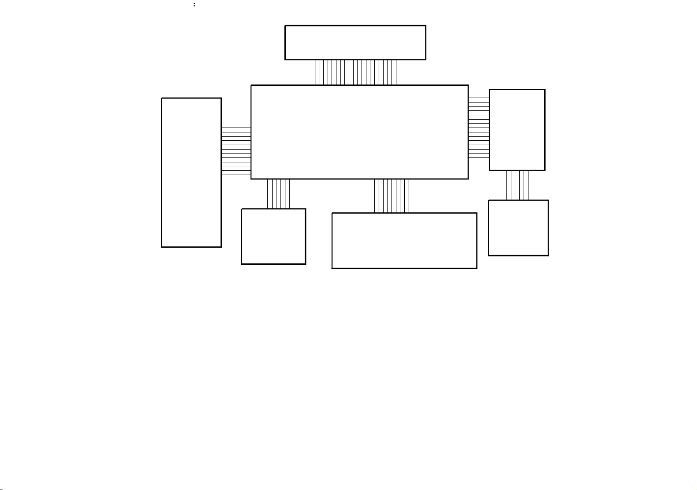
Figure 1 Schematic Diagram(TD-F61/F62/F63/F70)
AV BOARD
MAIN BOARD
DVD LOAD
Page 4
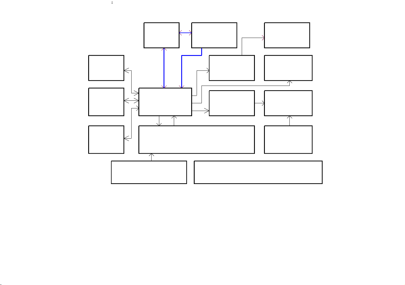
Figure 2 Basic Circuit Diagram
FLASH
EEPROM
AUDIOAMP&LPF
VIDEOD/A
CS4954/4955
PT6312(TD-F50/F61/F62/F63)/PT6554(TD-F70/F71)
WM8746
2402
SDRAM
REMOTEHANDSET
MT1369
VFD/KEY
1M*8
PT2222-001
VIDEOLPF&
DRIVE
SPDIFOUT
TOP233Y(TD-F50/F61/F62/F63)TEA1523P(TD-F70/F71)
RF
POWERSUPPLY
2*16Mbit
PT2399ECHO
MC4558
DECODER&SERVO
D L OV AD D
M C 4 5 5 8M I CA M P
A U D I OD / A
MT1336
DVD LOAD
WM8746
AUDIO D/A
VIDEO D/A
CS4954/4955
POWER SUPPLYREMOTE HANDSET
VIDEO LPF
& DRIVE
SPDIF OUT
MC4558
AUDIO AMP&LPF
Pt2399 ECHO
MC4558 MIC AMP
Page 5
a. Principle of power supply operating
Adopts switched-mode power supply module TOP233Y of TOPSWITCH company, it can protect
itself from over current, overheating, and short-circuit, etc. This circuitry mainly stabilizes at +5V,
and fluctuates within a permissible range, such as +5V, VA+, VA-, +3.3V and -24V. Please pay
attention to the high voltage inside the white paint of PCB while repairing. When using an oscillator
to measure this portion, an isolated transformer must be connected.
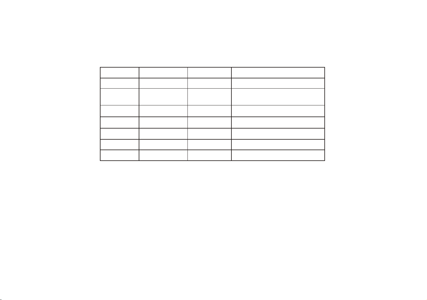
Circuit of power supply may output the following power sources:
Rated Voltage
VCC
+ 5V
+ 3.3V
VA+
VA-
-24V
AC1-AC2
Permissible Range Working Current Working Load
+ 4.75V ~ 5.45V
4.75V ~ 5.45V
3.20V ~ 3.46V
+8V +/-10%
-8V +/-10%
-20V ~ -25V
AC 2.8V ~ AC 3.5V
17mA Front board and muting circuit
520mA
650mA
15mA
15mA
10mA
80mA
Loader servo, motor driver, laser circuit,
audio D/A and T F circuit
Decoder board
Audio & Karaoke circuit
Audio & Karaoke circuit
Bias voltage of VFD on front board
Filament of VFD on front board
b. Troubleshooting and service
a). If +5V voltage varies out of the permissible range, check whether sampling resistance R8 and
R9 (R422 and R423) are eroded, and whether the 1st pin of regulated voltage reference U3 (U402)
TL431 is at 2.5V. If the deviation is over 0.1V, TL431 is eroded and shall be replaced. During
maintenance, the +5V sampling circuit, i.e. D9, R5, R8, R9 and U4 (D415, R419, R422, R423, R421
and U403), shall not be open, otherwise, it may result in high voltage and damage other circuits on
the rear pole.
b). If all the output voltage is 0V, and a voltage of 300V or so exists at the positive pole of C8 (C403),
check whether +5V, +8V, -8V, -24V and +3.3V are short (whether Q401, Q402 and Q403 are open).
c). If +3.3V of AC1-AC2 is 0V and no display on VFD, check whether D6 (D408) is open. If the ribb
on wire is not in good contact, replace the corresponding ribbon wire.
Note: Components in the brackets are of TDE-F70/F71.
2. Troubleshooting and Service of the Loader
Page 6

pole of Q1 and Q2, and whether U2 and adjacent parts are damaged or weld falsely.
d). If the above parts are normal and no laser emits, replace the loader.
b. Read no disc
a). Check whether the ribbon wire from 24P to loader is in good contact.
b). Check whether the RFO signal of the 10th pin of CN6 is transmitted to the 96th pin of U1.
c). Check whether laser voltage (about 2V for VCD and 2.2V for DVD respectively) exists at the C
pole of Q1 and Q2, and whether the voltage is normal.
d) Check whether U1, U2 and adjacent parts are damaged or weld falsely.
e). If the above parts are normal, replace U1 or the loader.
c. Read DVD discs only or read other discs beyond DVD only
a). Check whether the ribbon wire from 24P to loader is in good contact.
b). Check whether laser voltage of 2V outputs at the C pole of Q2, and whether the 125th pin of U1
is at low level.
c). Check whether the pins from the 1st to the 38th of U1 and adjacent parts are weld falsely,
damaged or erode.
d). If the above parts are normal, replace U1 or the loader.
3. Troubleshooting and service of decoding part
a. No video, no audio, no display on VFD, and no operation of keys
a). Check whether the power sources of the decoder board are normal.
b). Check whether there is 27MHz signal output. If not, X1 crystal and adjacent parts are eroded or
damaged.
c). Check whether there is 81MHz signal output at R64. If not, check whether there is short circuit,
false welding or alien substance for audio D/A circuit U5 and SDRAM U8 and U9.
d). Check whether the reset circuit composed of C7, R37 and D1 is normal (constant 0V after tens
of milliseconds of high level). If it is at low level constantly, C7, R37 and D1 are damaged.
e). If the reset level is normal, check whether the chip selection signal, address and data of the 12th
pin of U5 are normal.
f). Check U10 that whether the data of pins from the 1st to the 8th, hsync and vsync signal of the
10th and 11th pins, and 27MHz signal of the 29th pin are normal, and whether C162 and R68 are
normal. If not, replace U10.
g). When U5 works normally, check the connection between U8, U9 and U3. If abnormal, replace U8
or U9.
Page 7

Check U10 that whether the data of pins from the 1st to the 8th, hsync and vsync signal of the 10th and 11th
pins, and 27MHz signal of the 29th pin are normal, and whether C162 and R68 are normal. If not, replace U10.
2). Abnormal color of the video picture
a). If there are horizontal or vertical streaks, or improper color appears on the picture after reading a disc, the
U3 decoding servo chip on the decoder board or U6 EEPROM may be in problems.
b). Check board whether the 3.3V and 2.5V power sources are normal, whether the ripple factor is too high,
and whether the data wire of Y(0, 7) between U3 and U10 is normal.
c). Check whether the video filter network circuit on the decoder board works normally.
5. Troubleshooting and service of audio part
a. Normal picture, no sound
a). Firstly, check whether the +8V and -8V power sources for the operational amplifier IC U12~U14 are normal.
b). Check whether the C poles of muting tube Q14, Q15, Q22, Q23, Q21 and Q20 are at low level constantly.
If so, the above tubes are not in good conditions.
c). Check whether the output of C poles of Q18 and Q19 are at high levels constantly. If so, Q18 and Q19 have
been broken down, or C209 are short.
d). Check whether the six audio signal lines on the 20P ribbon wire from decoder board to output board are in
good contact. If abnormal, replace the ribbon wire. Check the signal reaching the input of U12~U14. If the input
is normal while the output is not, replace the operational amplifier IC.
e). Check whether the signals of the 17th, 19th, 21st, 23rd, 25th and 27th pins of U5 on the decoder board are
normal. If not, check the signals of the pins from the 2nd to the 7th. If the clock signals of ACLK, ABCK and
ALRCK output by U3 are normal after R130, RN2 and R131 are disconnected, replace U11.
b. Distorted audio and loud noise
a). Firstly, check whether the +8V and -8V power sources for the operational amplifier IC U12~14 are normal.
b). Check whether the muting tubes are in good conditions.
c). Check whether the signals of the 17th, 19th, 21st, 23rd, 25th and 27th pins of U11 on the decoder board are
normal. If not, check the signals of the pins from the 2nd to the 7th. If the clock signals of ACLK, ABCK and
ALRCK output by U1 are normal after R130, RN2 and R131 are disconnected, replace U5.
c. Pop noise during ON/OFF
Check whether the MUTE signal line on the output board is broken, then check whether Q18, Q19, muting tubes
and adjacent parts are damaged or eroded.
6. Troubleshooting and service of KARAOKE part
a. Microphone with sound but no echo
a). Check whether the level of the 1st pin of U1 on the KARAOKE board is +5V. If not, check whether JP1 is
damaged.
b). If the voltage is proper, check whether there is anything wrong with the adjacent parts of U1.
b. No sound of microphone
a). Check whether the microphone indicator on VFD lights. If the level of C pole of Q16 is low, the C and E poles
of Q16 are short.
b). Check whether the power source of U2 on the KARAOKE board is normal and with microphone signal output.
If not, check whether the parts of input circuit for microphone jack are damaged and check whether the
microphone jack is rusty or short.
Page 8

7. Full screen display or no display on VFD
a). Full screen display on VFD is often caused by abnormal -24V bias voltage. Check whether D5, C19 and R17
are disconnected.
b). If there is no display on VFD, firstly, check whether the filament lights in red. If not, and there is no 3.3V
voltage difference between AC1 and AC2, check whether D6, C9 and R21 are damaged. If the filament is not
red, while 3.3V voltage difference exists between AC1 and AC2, replace VFD.
c). If -24V and AC1-AC2 voltage are normal, check whether there are CS, DATA and CLK signals from CN301
on the front board. Then replace PT16312 (PT6554) under the condition that both of the above mentioned are
normal.
8. No operation of some keys on the front board, disordered display on VFD
Check whether the welding from the 12th, 13th, 15th pins of U301 to the 37th pin is in good conditions.
Check whether D301~D303 on the front board are damaged, whether circuit is disconnected, and whether R309,
R310 and R311 are open.
9. No sensitive remote reception, or no reception from the remote handset
Check whether the power source of the remote sensor is proper.
Check whether the remote handset is in good operation mode.
Use an oscillator to observe whether there is output wave from the 1st pin IR of the sensor after each pressing
of keys on the remote handset. If the remote handset is good, while no output from the sensor, the sensor is
damaged.
10. The machine can not be turned on or off
If the machine can not be turned on or off after pressing the STANDBY key on the remote handset and the
POWER key on the front board, replace the main chip U3.
Note: The above information is only for reference. If there is any mistake, please feel free to point out.
Page 9

Servo schematic circuit 1
CN6
1
GND
V20
2
Vc
3
C10 0.1u
VCC
E
4
E
F
5
F
D
6
D
A
7
A
B
8
B
C
9
C
RFO
10
RFO
11
GND
12
MDI1
PDc
13
NC
R1 100
14
VR
15
LDc
16
LDd
17
GND
R2 100
18
VR
L20
19
VCC
FB / 0805
PDd
FO+
FOTR+
TR-
HOP1200/0.5mm,24P
R30
1,0805
R17 20k
C58
150p
R21 390R
TROPEN
20
21
22
23
24
C57
0.1u
SL+
SL-
+5V
R22
1K
C11
0.1u
R29
1,0805
R26
220(0805)
FMSO
TRSO
V1P4
STBY
C59
390P
MDI2
+5V
AVCC
L15
10uH,DIP
C56
0.1u
Q3
9012
(TO92)
Q5
9013
8
OPO
OPOP+
RFO
RVCCIN
C24 1u
C26 1u
R18
20k
R35
0(0805)
R32
0(open)
C17 0.1u
C22 1u
C54
150p
RFVCC1
RFVCC
C18 0.1u
C19 0.1u
C20 0.1u
C21 0.1u
DD
CC
BB
AA
DMSO
DV33
+C7
10u
+5VP
DV33
MC
ML
MD
MICD
URST
HTRC [ 2 ]
RFRP [ 2 ]
BDO [ 2 ]
TEO [ 2 ]
CSO [ 2 ]
RFL
FEO
V1P4 [ 2 ]
V2P8 [ 2 ]
RFON [ 2 ]
RFOP [ 2 ]
TROPEN[ 2 ]
PWMOUT2[ 2 ]
FMSO [ 2 ]
TRSO [ 2 ]
FOSO [ 2 ]
DMSO[ 2 ]
SDEN [ 2 ]
SCLK [ 2 ]SCLK
SDATA[ 2 ]
ADIN[ 2 ]
+5V
+5VP
R37
10k
[ 2,3,4,5]
URST
AVCC
L16
C37
0.033u
FB / 0805
L17
FB / 0805
L18
FB / 0805
D1
1N4148
+5VP
DV33
MC
ML
MD
MICD
C43
+
10u
URST
HTRC
RFRP
BDO
TEO
CSO
RFL
FEO
V1P4
V2P8
RFON
RFOP
TROPEN
PWMOUT2
FMSO
TRSO
FOSO
DMSO
SDEN
SDATA
ADIN
+5V
R34
0(0805)
R9 27k
C30 27p
C31 0.015u
R10 100k
C36
470p
C41
C40
+
10u
0.1u
CN9
2
1
2PIN*2.0 180
CN10
2
1
2PIN*2.0(OPEN)
C42
0.1u
RVCC
RFVCC1
+
R33
C6
0(open)
100u
C27
0.1u
65
AGNDF
66
VCON
67
AVDDF
68
AGNDX
69
AVDDM
70
COSPHI
71
HALLCOS
72
REFCOS
73
AGNDM
74
HALLSIN
75
REFSIN
76
SINPHI
77
SW0
78
SW2
79
SW1
80
MOP
81
MON
82
AGNDX
83
AGNDX
84
CEON
85
CEOP
86
RFGCI
87
RFGCU
88
RFFGC
89
OSP
90
OSN
91
CDD
92
CDC
93
CDB
94
CDA
95
DVDRFIN
96
DVDRFIP
97
DVDD
98
DVDC
99
DVDB
100
DVDA
101
MA
102
MB
RVCCIN
C52 (open)
R15
750k
R14
330k
R87
1(0805)
SPSP+
C28
0.1u
SDATA
SDEN
URST
TRCLOSE
PWM OUT2
SCLK
64
AVDDP
IOB
RST
SCLK
VDDS
SDEN
GNDS
SDATA
AGNDX
AGNDP
XCK16M
DPDMUTE
MT1336E
SVDD
CDFON
CDFOPSDSC
AVDDIRAGNDSBSAMDMC
114
113
112
111
110
109
108
107
106
105
104
103
R11
33k
C50
C49
0.1u
0.1u
C53
200p
OPO
R16 0
R13
330k
CN8
2
1
TRIN
MICD
STBY
ENDM
LIMIT
TROUT
IO5
IO6
IO7
IO8
IO9
IOA
WAVDD
AGC1
WGAND
SGND
TNI
TPI
121
120
119
118
117
116
115
C47
0.015u
E
F
C48
0.1u
ADIN
OPOP+
R12
750k
V1P4
TRCLOSE
R5 10k
TROPEN
R6 10k
ENDM
R7 10k
STBY
R8 10k
RFVCC
39404142434445464748495051525354555657585960616263
U1
IO0
IO1
IO2
IO3
IO4
GND
38
UDGATE
HDGATE
VFO13
37
VDD
36
AGNDX
35
AGNDX
34
AGNDX
33
DPFO
32
DPFN
31
GNDP
30
HTRC
29
TRLP
28
TRLPA
27
CRTPLP
26
CRTP
25
HRFRP
24
LRFRP
23
DEFECT
22
VDDP
21
TEO
20
CSO
19
LVL
18
FEO
17
V20
16
VREFO
15
V2REFO
14
AVDDT
13
TM4
12
AGNDT
11
TM3
10
TM2
9
TM1
8
AGNDO
7
RFON
6
RFOP
5
AVDDO
4
AGNDX
3
AGNDX
2
WVDD
1
WOBSO
WGND
RFSUBO
LDO2
LDO1
MDI1
MDI2
AGC3
AGC2
MT1336E
128
127
126
125
124
123
122
LDO1
LDO2
MDI2
MDI1
C29
0.1u
HTRC
C32 10p
RFRP
C33 390p
BDO
C34 390p
C35
TEO
0.1u
CSO
RFL
FEO
V20
V1P4
V2P8
C39
C38 0.1u
0.1u
C44 0.1u
RFON
RFOP
RVCCIN
RVCCIN
C46
0.1u
SL+
SL-
LIMIT
2P,2.0mm,180
C55
10u
R36
0(0805)
RVCCIN
R31
0(open)
C
C23 1u
D
A
B
R27
1,0805
R19
10K
R20 20K
RVCC
C45
+
100u
C25 1u
C
D
A
B
AVCC
LDO_AVCC
L21
DV33
FB AXIAL(open)
C8
+
C9
0.1u
L19
10uH,DIP
Q1
S8550
R3 22
R4 22
Q2
S8550
U2
15
VOTK+
16
VOTK-
17
VOLD+
18
VOLD-
19
PGND
20
VNFTK
21
PVCC2
22
PREGND
23
VINLD
24
CTK2
25
CTK1
26
VINTK
27
BIAS
28
STBY
BA5954
+5V
R25
220(0805)
Q4
9012
LOAD+
LOADTRIN
TROUT
Q6
C60
9013
390P
VOFC+
VOFCVOSL+
VOSLPGND
PVCC1
VNFFC
VINSL-
VINSL+
VINFC
VCC
VOSL
CF2
CF1
GND
R23 390R
R24
1K
Important
100u
reduce
Noise
C12
+
47u
C13
+
47u
14
13
12
11
10
9
8
7
6
5
4
3
2
1
CN7
5
4
3
2
1
HEADER-5 (2mm)
TRCLOSE
LDO2
LDO_AVCC
LDO1
R28
1,0805
+5V
SPSP+
V1P4
FOSO
+
Page 10

9
R45 8.2k
C85 10n
C87 10n
R46 750k
R47 33k
R49 0
R50 10k
R51 15k
C94
0.01u
CSO
FEO
RFL
RFRP
RFZC
RFRPC
TEO
ADIN
RFON
RFOP
AV33
AV33
C73 20p
C74 20p
C75 1000p
C76 1000p
C86 10n
C88 10n
R56
4.7
V25
GND
GND
DV33
V25
C63
+
47u
R39 (open)
A8
A9
A10
A11
A12
A13
A14
A15
AD7
AD6
AD5
AD4
AD3
AD2
AD1
AD0
A0
A1
A2
A3
A4
A5
A6
A7
A16
A17
A18
A19
+
C95 10u
C65
C64
0.1u
0.1u
R40 100k
C77
150p
RFIN
RFIP
208
207
206
U3
RFIP
RFIN
1
RFDTSLVN
IREF
2
PLLVSS
3
LPIOP
4
LPION
5
LPFON
6
LPFIP
7
LPFIN
8
LPFOP
9
JITFO
10
JITFN
11
PLLVDD3
12
FOO
13
TRO
14
TROPENPWN
15
PWMOUT2
16
DVDD2
17
DMO
18
FMO
19
FG
20
DVSS
21
HIGHA0
22
HIGHA1
23
HIGHA2
24
HIGHA3
25
HIGHA4
26
HIGHA5
27
DVSS
28
HIGHA6
29
HIGHA7
30
AD7
31
AD6
32
AD5
33
AD4
34
DVDD3
35
AD3
36
AD2
37
AD1
38
AD0
39
IOA0
40
IOA1
41
DVDD2
42
IOA2
43
IOA3
44
IOA4
45
IOA5
46
IOA6
47
IOA7
48
A16
49
A17
50
IOA18
51
IOA19
52
DMVSS
DMVDD3
ALE
IOOE#
5354555657585960616263646566676869707172737475767778798081828384858687888990919293949596979899
PRD #
C96 22pF
R54
100K
C97 22pF
R880R
L23
C98
OPEN(2.2uH)
OPEN(1000pF)
V1P4
C66
0.1u
C69
0.1u
C67
R41
1000p
C78
150p
205
204
203
SCOP
SCON
RFDTSLVP
18k
C68
1000p
DV33
SCLK
SDEN
BDO
202
201
200
199
198
197
196
195
194
193
192
191
TEI
FEI
CSO
HRFZC
RFSUBI
TEZISLV
RFLEVEL
RFRPSLV
RFRP_AC
ADCVDD3
RFRP_DC
SDA TA
190
189
188
187
186
185
184
183
182
181
BDO
ADIN
SLCK
SDEN
SDATA
DVDD3
ADCVSS
PDMVSS
PDMVDD3
PWMVREF
PWM2VREF
MT1369E_208
IOWR#
IOCS#
DVSS
UP1_2
UP1_3
UP1_4
UP1_5
UP1_6
DVDD3
UP1_7
UP3_0
UP3_1
INT0#IRDVDD2
UP3_4
UP3_5
UWR#
URD#
XTALI
XTALO
DVSS
RD7
RD6
RD5
PCE#
VSTB
MD
VSCK
SCL
PWR#
VSDA
SD A
DV33
MICD
GND
1369P3_1
R52
R158
33R(open)
0R
X1
27MHz
1
2
3
4
5
6
7 8
RxD
IR
TxD
V25
U4
14
13
12
11
10
9
74HCU04(open)
R159
0R
DQ7
DQ5
DQ6
GND
R160
33R
DV33
R5333R
180
179
WOBSI
RD4
DQ4
V25
C99
0.1u(open)
DV33
C70
+
47u
RESET#
R42
GND
V25
DV33
Y1
Y0
Y4
Y5
Y3
Y2
Y6
Y7
URST
178
177
176
175
174
173
172
171
170
169
168
167
166
165
164
ICE
PRST
DVSS
YUV7
YUV6
YUV5
YUV4
YUV3
YUV2
YUV1
VFO13
DVDD3
IFGATE
UDGATE
DVDD2/3
RD3
RD2
RD1
RD0
WE#
DQ3
DQ1
DQ0
DQ2
27MHZ
YUV0
DVDD2
RWE#
CAS#
RAS#
RCS#
BA0
DVDD3
RD15
RD14
RD13
RD12
DVSS
CAS#
RAS#
CS#
BA0
DQ12
DQ15
DQ13
DQ14
GND
DV33
10k
GND
VSYNC#
HSYNC#
163
162
161
160
DVSS
VSYN
HSYN
RD11
RD10
RD9
100
101
DQ8
DQ11
DQ9
DQ10
AV33
+
ASPDIF
159
158
157
SPDIF
BLANK#
MC_DAT
156
APLLVDD3
APLLVSS
155
ACLK
154
ASDATA2
153
ASDATA1
152
ASDATA0
151
DVDD3
150
ALRCK
149
ABCK
148
RD16
147
RD17
146
DVSS
145
RD18
144
RD19
143
RD20
142
RD21
141
DVDD2
140
RD22
139
RD23
138
DQM2
137
DQM3
136
DVSS
135
RD24
134
RD25
133
RD26
132
RD27
131
DVDD3
130
RD28
129
RD29
128
RD30
127
RD31
126
DVSS
125
RA3
124
RA2
123
RA1
122
RA0
121
DVDD2
120
RA10
119
BA1
118
DQM0
117
DQM1
116
DVSS
115
RA4
114
RA5
113
RA6
112
RA7
111
DVDD3
110
RA8
109
RA9
108
RA11
107
CKE
106
CLK
105
DVSS
RD8
VPVDD3
VCOCIN
VPVSS
102
103
104
C100
0.1u
+
C101 10u
R55
4.7
VSCK
VSCK
VSDA
VSDA
URST
URST
HTRC
HTRC [ 2 ]
RFRP
RFRP [ 2 ]
BDO
BDO [ 2 ]
TEO
CSO
RFL
FEO
V20
V1P4
V2P8
RFON
RFOP
TROPEN
PWMOUT2
FMSO
TRSO
FOSO
DMSO
SDEN
SCLK
SDATA
ADIN
TEO [ 2 ]
CSO [ 2 ]
RFL
FEO
V20 [ 2 ]
V1P4 [ 2 ]
V2P8 [ 2 ]
RFON [ 2 ]
RFOP [ 2 ]
TROPEN[ 2 ]
PWMOUT2[ 2 ]
FMSO [ 2 ]
TRSO [ 2 ]
FOSO [ 2 ]
DMSO[ 2 ]
SDEN [ 2 ]
SCLK [ 2 ]
SDATA[ 2 ]
ADIN[ 2 ]
VSDA
VSCK
VSTB
IR
R59 10
R58 10
R57 10
R60 10
C71
0.1u
R44
4.7
C81
C80
+
100p
47u
FOSO
TRSO
TROPEN
PWMOUT2
DMSO
FMSO
C91
C90
V1P4
-24V
F+
F-
VCC5
VCC5
C103
PCON
100p
+5VP
PMUTE
C102
120pF
CN4
SERIA L/UP/4P,2.0m/m
1
2
3
4
5
6
7
8
9
10
11
12
13
CN5
CON13*2.0
DV33
4
RxD
3
TxD
2
1
DV33
C106
C105
C104
0.1u
0.1u
0.1u
V25
C111
C112
C113
0.1u
0.1u
0.1u
330p
open
C107
C108
0.1u
0.1u
C114
C115
0.1u
0.1u
R38 0
HTRC
V2P8
C72
+
47u
C84
C83
C82
10n
1u
0.1u
C89 100p
C93
C92
0.015u
330p
C110
C109
0.1u
0.1u
C116
0.1u
Servo schematic circuit 2
L22
AV33
FB AXIAL
AV33
R43
4.7AV33
C79
10u
ACLK
ASDAT2
ASDAT1
ASDAT0
DV33
ALRCK
ABCK
DQ16
DQ17
GND
DQ18
DQ19
DQ20
DQ21
V25
DQ22
DQ23
DQM2
DQM3
GND
DQ24
DQ25
DQ26
DQ27
DV33
DQ28
DQ29
DQ30
DQ31
GND
MA3
MA2
MA1
MA0
V25
MA10
BA1
DQM0
DQM1
GND
MA4
MA5
MA6
MA7
DV33
MA8
MA9
MA11
DCKE
DCLK
GND
ASDAT[0..2]
RST#
VSCK
VSDA
V25
DV33
RESET#
1369P3_1
27MHZ
URST
Y[0..7]
HSYNC#
VSYNC#
ASPDIF
ACLKR48 33k
ALRCK
ABCK
A[0..19]
AD[0..7]
PRD#
PWR#
PCE#
MA[0..11]
BA[0..1]
DQ[0..31]
DQM[0..3]
RAS#
CAS#
CS#
WE#
DCLK
DCKE
SCL
SDA
MICD
MD
V25
DV33
RESET#
1369P3_1
27MHZ
URST
RST#
Y[0..7]
HSYNC#
VSYNC#
ASPDIF
ACLK
ALRCK
ABCK
ASDAT[0..2]
A[0..19]
PRD#
PWR#
PCE#
MA[0..11]
BA[0..1]
DQM[0..3]
RAS#
CAS#
WE#
DCLK
DCKE
VSCK
AD[0..7]
DQ[0..31]
SCL
SDA
MICD
MD
VSDA
(5)
(1)
(5)
(4)
(4)
(4)
(4)
(4)
(4)
(4)CS#
(4)
(4)
(4)
(4,5)
(4,5)
(4)
(5)
(5)
(5)
(5)
(5)
(5)
(5)
(5)
(4)
(4)
(4)
(4)
(4)
(4)
Page 11

Decoder schematic circuit 1
(3)
DCLK
DCLK
DCKE
DCKE
(3)
(3)
CAS#
CAS#
RAS#
RAS#
(3)
WE#
WE#
(3)
CS#
CS#
(3)
MA[0..11]
(3)
MA[0..11]
(3)
BA[0..1]
BA[0..1]
DQ[0..31]
(3)
DQ[0..31]
DQM[0..3]
(3)
DQM[0..3]
PCE#
PCE#
(3)
PRD#
PRD#
PWR#
PWR#
(3)
A[0..19]
A[0..19]
(3)
AD[0..7]
AD[0..7]
(3)
SCL
SCL
(3,5)
(3,5)
SDA
SDA
RST#
RST#
GNDV
GND
CVBS
CVBS
Sy
Sy
Sc
Sc
Y/G
Y/G
Pr/B
Pr/B
Pb/R
Pb/R
Y[0..7]
27MHZ
RESET#
U10
29
CLOCK
34
RESET
Y0
1
V0
Y1
2
V1
3
Y2
V2
Y3
4
V3
Y4
5
V4
Y5
6
V5
Y6
7
V6
Y7
8
V7
26
PDAT0
25
PDAT1
24
PDAT2
23
PDAT3
22
PDAT4
21
PDAT5
20
PDAT6
19
PDAT7
27
RD
28
WR
30
TTXDAT
31
TTXRQ
12
INT
L14
FB AXIAL
32
SDA
33
SCL
13
TEST
14
XTALOUT
15
XTALIN
16
PADDR
CS4954
V33
C117
47UF
SDA
SCL
DV33
C118
0.1UF
FIELD/CB
HSYNC/CB
VSYNC
GREEN
GNDD
GNDA
GNDA
GNDA
V33
17
VDD
36
VAA
41
VAA
46
VAA
38
VREF
9
10
11
44
CVBS
48
Y
47
C
39
RED
40
43
BLUE
37
ISET
18
35
42
45
C119
0.1UF
0.1UF
C120
(1,2,3,5,6)
27MHZ
(3)(3)
(3)
HSYNC#
(3)
VSYNC#
Y[0..7]
(3)
RESET# RESET#
(1)
V33
C162
0.1UF
R66 10 OHM
R67 10 OHM
R68
4K(1%)
C121
0.1UF
(1,2,3,5)
CVBS#
Y#
C#
R#
G#
B#
DV33
27MHZ
HSYNC#
VSYNC#
Y[0..7]
10
U7
DMA0
23
A0
24
+5VP
+5VP
DV33
SDA
SCL
A0
A1
A2
A3
A4
A5
A6
A7
A8
A9
A10
A11
A12
A13
A14
A15
+5VP
A16
A17
A18
R63
4.7K
C138 22pF
Y#
L12 2.2uH
C137
R72
470pF
HSYNC#
VSYNC#
75R
C135 22pF
R#
L9 2.2uH
C134
R78
470pF
75R
C132 22pF
G#
L10 2.2uH
R81
75R
C131
470pF
C133
470pF
R62
R61
680R
680R
C140
0.1uF
U5
11
A0
10
A1
9
A2
8
A3
7
A4
6
A5
5
A6
4
A7
42
A8
41
A9
40
A10
39
A11
38
A12
37
A13
36
A14
35
A15
34
A16
3
A17
2
RY/BY/A18
1
NC / RD/BY
PCE#
12
CE
PRD#
14
OE
PWR#
44
RESET
AM29F400BT-120SC/800BT-120SC
R73
C139
BAT85
470pF
R79
BAT85
C136
470pF
R82
BAT85
+5VP
+5VP
BYTE
GND1WE
GND2
D0
D1
D2
D3
D4
D5
D6
D7
D8
D9
D10
D11
D12
D13
D14
D15
VCC
R83
BAT85
Q11
9012(open)
EEPROM
U6
8
VCC
7
WC
6
SCL
24C01A
15
17
19
21
24
26
28
30
16
18
20
22
25
27
29
31
33
23
1343
32
1
S0
2
S1
3
S2
45
GNDSDA
AD0
AD1
AD2
AD3
AD4
AD5
AD6
AD7
A19
+5VP
C143
10uf/16v
C142
0.1UF
+5VP
R74
BAT85
Sy
Q8
9012(open)
+5VP
R80
BAT85
Pb/R
Q10
9012(open)
Y/G
CS#
RAS#
CAS#
WE#
BA0
BA1
DCLK
DCKE
MA0
MA1
MA2
MA3
MA5
MA6
MA7
MA8
MA9
MA10
MA11
DQM0
DQM2
DQM1
DQM3
RN1 33x4
1 2
3 4
5 6
7 8
R64 33
R65 33
DV33
SD33
+
DCS#
DRAS#
DCAS#
DWE#
DBA0
DBA1
SDCLK
SDCKE
DMA0
DMA1
DMA2
DMA3 RDQM0
DMA4MA4
DMA5
DMA6
DMA7
DMA8
DMA9
DMA10
DMA11
RDQM0
RDQM2
RDQM1
RDQM3
L13
SD33
+C145
C144
47u
0.1u
FB / 0805
SD33
C149
C148
C150
0.1u
0.1u
C146
47u
SD33
C155
0.1u
0.1u
C158
C157
C156
0.1u
0.1u
0.1u
RDQ0
DQ0 DMA4
RDQ1
DQ1
RDQ2
DQ2
DQ3
RDQ3
RDQ4
DQ4
RDQ5
DQ5
RDQ6
DQ6
DQ7
RDQ7
DQ8
RDQ8
DQ9
RDQ9
DQ10
RDQ10
RDQ11
DQ11
RDQ12
DQ12
DQ13
RDQ13
RDQ14
DQ14
RDQ15
DQ15
RDQ16
DQ16
DQ17 RDQ17
DQ18
RDQ18
RDQ19
DQ19
RDQ20
DQ20
RDQ21
DQ21
RDQ22
DQ22
DQ23
RDQ23
DQ24
RDQ24
DQ25
RDQ25
DQ26
RDQ26
RDQ27
DQ27
DQ28
RDQ28
RDQ29
DQ29
RDQ30
DQ30
DQ31
RDQ31
C152
C151
C153
0.1u
0.1u
0.1u
C159
C160
0.1u
0.1u
C154
0.1u
DMA1
DMA2
DMA3
DMA5
DMA6
DMA7
DMA8
DMA9
DMA10
DMA11
DBA0
DBA1
SDCLK
SDCKE
DCS#
DRAS#
DCAS#
DWE#
RDQM1
DMA0
DMA1
DMA2
DMA3
DMA4
DMA5
DMA6
DMA7
DMA8
DMA9
DMA10
DBA0
SDCLK
SDCKE
DCS#
DRAS#
DCAS#
DWE#
RDQM0
RDQM1
DMA0
DMA1
DMA2
DMA3
DMA4
DMA5
DMA6
DMA7
DMA8
DMA9
DMA10
DBA0
SDCLK
SDCKE
DCS#
DRAS#
DCAS#
DWE#
RDQM2
RDQM3
A1
25
A2
26
A3
29
A4
30
A5
31
A6
32
A7
33
A8
34
A9
22
A10/AP
35
A11
20
BA0/A13
21
BA1/A12
38
CLK
37
CKE
19
CS
18
RAS
17
CAS
16
WE
15
DQML
39
DQMHNCVCCQ
36
NC
40
54
VSS
41
VSS
28
VSS
SDRAM
21
22
23
24
27
28
29
30
31
32
20
19
35
34
18
17
16
15
36
33
37
26
50
(open)
U9
A0
A1
A2
A3
A4
A5
A6
A7
A8
A9
A10
BA/A11
CLK
CKE
CS
RAS
CAS
WE
DQMHNCVCCQ
NC
VSS
VSS
SDRAM
U8
21
A0
22
A1
23
A2
24
A3
27
A4
28
A5
29
A6
30
A7
31
A8
32
A9
20
A10
19
BA/A11
35
CLK
34
CKE
18
CS
17
RAS
16
CAS
15
WE
36
DQMHNCVCCQ
33
NC
37
26
VSS
50
VSS
SDRAM
2
RDQ0
DQ0
4
RDQ1
DQ1
5
RDQ2
DQ2
7
RDQ3
DQ3
8
RDQ4
DQ4
10
RDQ5
DQ5
11
RDQ6
DQ6
13
RDQ7
DQ7
42
RDQ8
DQ8
44
RDQ9
DQ9
45
RDQ10
DQ10
47
RDQ11
DQ11
48
RDQ12
DQ12
RDQ13
50
DQ13
51
RDQ14
DQ14
53
RDQ15
DQ15
SD33
1
VCC
14
VCC
27
VCC
SD33
3
VCCQ
9
VCCQ
43
49
VCCQ
6
VSSQ
12
VSSQ
46
VSSQ
52
VSSQ
RDQ0
2
DQ0
RDQ1
3
DQ1
RDQ2
5
DQ2
RDQ3
6
DQ3
RDQ4
8
DQ4
RDQ5
9
DQ5
RDQ6
11
DQ6
12
RDQ7
DQ7
39
RDQ8
DQ8
RDQ9
40
DQ9
RDQ10
42
DQ10
RDQ11
43
DQ11
RDQ12
45
DQ12
RDQ13
46
DQ13
RDQ14
48
DQ14
RDQ15
49
DQ15
SD33
1
VCC
25
VCC
SD33
7
VCCQ
1314
VCCQDQML
38
44
VCCQ
4
VSSQ
10
VSSQ
41
VSSQ
47
VSSQ
RDQ16
2
DQ0
RDQ17
3
DQ1
RDQ18
5
DQ2
RDQ19
6
DQ3
RDQ20
8
DQ4
RDQ21
9
DQ5
RDQ22
11
DQ6
RDQ23
12
DQ7
RDQ24
39
DQ8
RDQ25
40
DQ9
RDQ26
42
DQ10
RDQ27
43
DQ11
RDQ28
45
DQ12
RDQ29
46
DQ13
RDQ30
48
DQ14
RDQ31
49
DQ15
SD33
1
VCC
25
VCC
SD33
7
VCCQ
1314
VCCQDQML
38
44
VCCQ
4
VSSQ
10
VSSQ
41
VSSQ
47
VSSQ
+5VP
R86
C123 22pF
B#
L11 2.2uH
R84
75R
C122
470pF
R85
BAT85
C124
470pF
BAT85
Q12
9012(open)
Pr/B
C#
C126 22pF
L7 2.2uH
R75
C125
75R
470pF
C127
470pF
BAT85
+5VP
R77
BAT85
Sc
Q9
9012(open)
R76
CVBS#
C129 22pF
L8 2.2uH
R69
C128
75R
470pF
+5VP
R71
BAT85
CVBS
Q7
9012(open)
R70
C130
BAT85
470pF
Page 12

11
1500pF
+5VP
C171
R112
10K
C175
1500pF
VA+1
84
U13A
3
4558
+
1
2
-
VA-1
R108
3.3K
R107
18K
R113
3.3K
R114
18K
SW
L
R
SL
SR
CN
SWASDT2
L6
2.2R
C195
100uF/16v
C172
150pF
VA+1
84
5
+
6
-
VA-1
C176
150pF
R118
10K
C179
1500pF
R124
10K
CN
+
C197
C196
0.1u
0.1u
Rs_OUT
U13B
4558
Ls_OUT
7
R119
3.3K
C180
150pF
R120
20K
R125
3.3K
R126
20K
C183
1500pF
VCCA
C198
0.1u
C173
10uF/16V(short)
C177
10uF/16V(short)
VA+1
84
3
+
2
-
VA-1
VA+1
5
6
C184
150pF
R109
0R
R110
C174
10K(open)
OPEN
MUTE
R116
0R
R115
10K(open)
MUTE
U14A
4558
1
84
U14B
4558
+
7
-
VA-1
R111
OPEN
R117
OPEN
LFE_OUT
C178
OPEN
C181
10uF/16V(short)
C_OUT
Q23
OPEN
LS
Q22
OPEN
C185
10uF/16V(short)
VA+1
84
3
+
2
-
R89
R
10K
C163
1500pF
R100
MIC
1369P3_1
PMUTE
R172 OPEN
+5V
VCC
R142 0R
VA+
VCC
2.2K
+5V
R151
OPEN(10K)
R133
0R
R134
OPEN(0R)
1N4148
MIC1
R104
10K
L
C167
1500pF
R146
R147
3.3K
R148 10k
Q26
OPEN(9015C)
R152
OPEN(10K)
R138
D5
0R
470uF/10v
R140
10K
D3
1N4148
R135
100K
R90
3.3K
C164
R91
150pF
18K
R101
10K
R99
10K
5
6
R102
3.3K
R103
18K
3.3K
Q17
OPEN(9015C)
R149
10K(open_)
Q18
9015C
C208
+
Q19
9015C
R136
10K
+
C209
10uF/16v
C168
150pF
R150
220R
D6
OPEN(1N4148)
MUTE
R137
100K
ALRCK
VA-1
R143
1K
C165
U12A
10uF/16V(short)
4558
1
VA-1
MUTE
84
C169
U12B
10uF/16V(short)
4558
+
7
-
VA-1
MIC1
Q16
9014C
R157
R145
10K(open)
10K
ML
MC
R161
R144
0R
0R(open)
VSDA
VSCK
ML
MC
MD
ABCK
ALCK
ASDT0
ASDT1
ASDT2
R139
0R(OPEN)
R141
0R(OPEN)
1
2
3
4
5
6
7
8
9
CN11
CON9*2.0(open)
ML
MC
MUTE
R93
0R
R92
10K(open)
R98
0R
R97
10K(open)
VCCA
R162
10K(open)
MD
R94
R1
0R(OPEN)
MAINR
C166
OPEN
Q14
OPEN
R95
OPEN
R96
L1
0R(OPEN)
MAINL
C170
OPEN
Q15
OPEN
R105
OPEN
VA+1
C201
C200
0.1uF
VA-1
C204
0.1uF
C202
0.1uF
0.1uF
C205
C206
0.1uF
0.1uF
Audio D/A
VSDA
VSCK
ACLK
ABCK
ALRCK
ASDAT[0..2]
R131 33R
R130 33R
RN2 33Rx4
1 8
2 7
3 6
4 5
ACLK
ABCK
ALRCK
ASDAT[0..2]
ML
MC
MD
MODE
VSDA
VSCK
VA+1
OPEN(100R)
VCCA
R132
100uF/16v(open)
R164
10K
MODE
R165
R163
0R(open)
0R
ABCK
ACLK
ALRCK
ASDT0
ASDT1
SR
C203
10uF/16V
C207
10uF/16V
U11
1
DVDD
AVDD1
AVDD2
11
DGND
AGND1
AGND2
12
LATCH/12S
13
SCLK/IWL
GR0
14
SDIN/DM0
GR1
9
MUTE
GR2
OUT0L
8
MODE
OUT0R
10
LRCLK2
OUT1L
2
MCLK
3
BCLK
OUT1R
4
LRCLK
5
DIN0
OUT2L
6
DIN1
7
DIN2
OUT2R
CAP
WM8746
U15
OPEN(78L05)
VCCA
13
+
2
C199
15
28
20
24
26
22
18
25
27
21
23
17
19
16
SL
VCCA
C187 10uf/16v
C188 10uf/16v
C190 10uf/16v
C192 10uf/16v
C191 10uf/16v
C189 10uf/16v
C193
0.1uF
C194
10uf/16v
R106
10K
Decoder schematic circuit 2
RS
CN1
MUTE
R122
0R
R121
10k(open)
MUTE
R123
OPEN
R128
0R
R127
10K(open)
1
2
3
4
5
6
7
8
9
10
11
12
CON12(2.5mm)
SUB
C182
OPEN
Q21
OPEN
C186
OPEN
R129
OPEN
Q20
OPEN
VCC
L1
FB AXIAL(OPEN)
C210
100uF/16v(OPEN)
CENT
+3.3V
+5V
FB AXIALVA+1
+
+
MICD
L2
C211
220uF/16v
HSYNC#
VSYNC#
L3
FB AXIAL
C212
+
220uF/16v
Pb/R
CVBS
L1
R153 OPEN(0R)
R154 0R
MIC
R1
R155 OPEN(0R)
R156 0R
L4
FERB(0805)
VA+1
VA-1
+5V
Y/G
Pr/B
Sc
Sy
VA+
VA-
PCON
FF+
-24V
MUTE
ASPDIF
R173 OPEN
L5
VCC5
+5VP
DV33
R171
0R
R174
OPEN
FERB(0805)
Q13 8050
MAINL
MAINR
LS
RS
SUB
CENT
+5VP
Sc
CVBS
Sy
VA+
VA-
100uF/16v
MIC/HL
MICD/HR
VA+1
VA-1
VCC
C213
CN2
1
2
3
4
5
6
7
8
9
10
11
12
13
14
15
16
17
18
19
20
con20(1.25)
VA+
VA-
+5V
V25
+
C214
0.1u
1
2
3
4
5
6
CN3
6PIN*2.5
Page 13

Front control board schematic circuit (HV-2000)
/CSTB
SG14
R307
100
S G 3 1
COM3
R316 100
C306
47P
R314 100
IR
SG 2 1
9
SG 7
SG29
STB+5V
S G 1 1
S G 4 0
S G 2 2
D301
STANDBY
NOTE_ST
GND
NOTE_ST
STB+5V
K307
SG12
S G 3
C305
47P
SG22
1
S G 5
S G 1 0
S G 3 4
C302
104
REM301
REM
1
2
3
IR
GND
VCC
S G 1 0
R310
10K
C O M 1
S G 3 3
R30410K
SG32
S G 2 8
S G 3 7
LCD
LCD301
124567891 0111 2
1 3
1 4
1 5
1 6
1 7
1 8
1 9
2 0
2 1
2 2
3
2 3
2 4
2 5
2 6
2 7
2 8
2 9
3 0
3 1
3 2
3 3
3 4
3 5
3 6
3 7
3 8
3 9
4 0
4 1
4 2
4 3
4 4
S G 2
2
S G 2 0
C311
680PF
R318
51K
C O M 3
S G 1 1
S G 5
R30210K
4
S G 4
S G 1 8
D303
1N4148
K304
S G 1 3
SG18
S G 3 6
C310
104
S G 3 8
CON302
SERI A L/ UP/ 4 P, 2. 0m/ m
4
3
2
1
S G 1
SG34
SG31
R313 100
6
S G 1 5
SG25
S G 3 9
S G 1 4
S G 6
SG27
S G 1 2
S G 2 4
COM2
R320
56K
R321
470R
R317
51k
COM4
SG21
D302
1N4148
SG28
K305
U301
PT6554
1
2
3
4
5
6
7
8
9
10
11
12
13
14
15
16
1 7
1 8
1 9
2 0
2 1
2 2
2 3
2 4
2 5
2 6
2 7
2 8
2 9
3 0
3 1
3 2
33
34
35
36
37
38
39
40
41
42
43
44
45
46
47
48
4 9
5 0
5 1
5 2
5 3
5 4
5 5
5 6
5 7
5 8
5 9
6 0
6 1
6 2
6 3
6 4
SG1/P1
SG2/P2
SG3/P3
SG4/P4
SG5
SG6
SG7
SG8
SG9
SG10
SG11
SG12
SG13
SG14
SG15
SG16
S G 1 7
S G 1 8
S G 1 9
S G 2 0
S G 2 1
S G 2 2
S G 2 3
S G 2 4
S G 2 5
S G 2 6
S G 2 7
S G 2 8
S G 2 9
S G 3 0
S G 3 1
S G 3 2
SG33
SG34
SG35
SG36
SG37
SG38
SG39
COM1
COM2
COM3
COM4
SG40/KS1
SG41/KS2
KS3
KS4
KS5
K S 6
K I 1
K I 2
K I 3
K I 4
K I 5
T E S T
V D D
V D D 1
V D D 2
V S S
O S C
D O
C E
C L K
D I
S G 4 0
7
K302
DO
C304
47P
DI
S G 6
S G 9
S G 3 6
standby
D304
1N4148
CLK
S G 1 7
R315 100
C308
104
S G 2
S G 2 5
R312
10K
S G 2 3
S G 7
SG30
SG26
S G 8
S G 4
S G 3 2
K303
SG16
SG24
S G 9
R319
51k
S G 1
R306
10K
SG15
+
C301
47uF/10v
8
COM[1..4]
SG 2 9
SG 3 7
LP301
LAMP
COM1
S G 8
S G 3 0
R30510K
C309
104
S G 1 9
SG13
R308
10K
+
C307
47uF/10v
CON301
9pin-2.0mm
3
S G 3
SG[1..40]
R309
10K
CON303
SERI A L/ UP/ 4 P, 2. 0m/ m
1
2
3
4
S G 2 6
SG35
S G 3 9
S G 3 8
SG19
K306
R30310K
5
SG20
S G 3 5
C O M 4
SG23
SG17
K301
R301
10K
S G 1 6
C O M 2
SG[1..40]
C303
47P
S G 2 7
SG33
12
Page 14

13
Front control board schematic circuit (HV-2100)
R320
4.7K
REM301
VCC
GND
IR
REM
CON301
1
2
3
4
5
6
7
8
9
10
11
12
13
CON13(2.0)
R316
10K
3
2
1
-24V
AC1
AC2
GND
VCCA
DATA
CLK
CS
IR1
GND
PCON
+5VP
P_MUTE
+
C311
10uF
IR
VCCA
D306
1N4148
C306
104
C301
104
U302
1
RA2
2
RA3
3
T0CKI
4
/MCLR
5
Vss
6
RB0
7
RB1
8
RB2
9 10
RB3 RB4
PIC16C54S
R307
100 ohm
+
C315
47uF
RA1
RA0
OSC1
OSC2
Vdd
RB7
RB6
RB5
VCCA
CS
CLK
DATA
R317
4.7K
18
17
16
15
14
13
12
11
D304
STANDBY
VCCA
R318
4.7K
R319
4.7K
POWOFF
LED
P_MUTE
C314
47P
470
R313
J1 SHORT
+5VP
R301 100 ohm
R302 100 ohm
R303 100 ohm
-24V
C302
104
R326
4.7K
IR
NOTE-STDBY
PCON
C313
47P
VCCA
Y1
R304
10K
R305
10K
C312
47P
IR
4MHz
R306
10K
+5VP
+
C308
C309
104
104
C310
47uF
R323
10K(OPEN)
R315
4.7k OHM(SHORT)
VFD301
HNV-06SS63T
F1F1NP6G5G4G3G2GNC1GNCP1P2P3P4NCNCP5P6P7P8NCNCP9P10
1234567981011121314151617181920212223242526272928303132333435
AC1
-24V
2324252627282930313233
G6
VCCA
R308
51K
Q301
9014C(
POWOFF
R324
10K(OPEN)
IR1
Q302
9014C(
SH OR T C-B)
34
G4
35
G3
36
G2
37
G1
38
VDD
39
LED4
40
LED3
41
LED2
42
LED1
43
GND
44
OSC
NOTE-STDBY
SHORT C-B)
G5
PT16312
SW1
1234567891011
SW2
SEG15
SEG16
U301
SW3
SW4
VEE
SEG9
SEG10
SEG11
SEG12
SEG13
SEG14
SDout
SDin
GND
SCLK
SEG8
SEG7
SEG6/K6
SEG5/K5
SEG4/K4
SEG3/K3
SEG2/K2
SEG1/K1
VDD
KEY4
KEY3
/CS
KEY1
KEY2
R312
10K
22
21
20
19
18
17
16
15
14
13
12
P11
P12
P13NCP14
P15
P16NPF2
F2
AC2
+5VP
D301
1N4148
K301
PRV
K304
STOP R311 10K
K302
K305
NEXT
PLAY
D302
1N4148
K303
PAUSE
K306
OPEN/CLOSE
D303
1N4148
R309 10K
R310 10K
Page 15

Karaoke schematic circuit
14
MIC2
1
2
3
MIC1
1
2
3
10K
RP2
VAM+
R1
C1
2.2K
R18
10K
R5
2.2K
C8
104
R19
1 M
104
1
1
2
3
1
2
3
R26
47K
R27
47K
2 3
R20
15K
R21
1.5K
R28
10K
R30
10K
V1
9014
R2
1.2K
C2
22UF/16V
C12
1UF/16V
R23
150K
3
2
R22
10K
84
+
-
C3
100UF/25V
C5
100UF/25V
C11
1UF/16V
C6
104
RP1
10K
R24
100
R25
3K3
VCC
M-DET
C14
4.7UF/50V
U2A
4558
1
47K
R3
C7
101
VAM-
C4
104
V2
9015 VCC
D1
IN4148
4.7UF/16V
C13
R8
15K
C15
332
C28
100UF/16V
C29
104
R9
10K
16
LPF1-IN
C17
4.7UF/50V
C16
561
15
VCC
1
R11
12k
R10
10K
LPF1-OUT
REF
2
C27
47UF/16V
C18
4.7UF/50V
C24
4.7UF/50V C9
C21
C19
OPEN/103
R12
5.1K
3
332
14
LPF2-OUT
U1
PT2399
AGND
DGND
4
C20
561
R16
1K
R13
10K
CLK-O
5
R17
13K
GND
VAM+
VAM-
VCC
R31
8.2K
13
LPF2-IN
MIN
M-DET
6
R6
1K
22UF/16V
R14
10K
12
VCO
OP2-OUT
R15
15K
C22
683
CC1
7
5
6
C26
104
11
U2B
84
4558
C30
1
2
3
4
5
6
R7
15K
C10
101
8
JP1
CC0
C25
104
SHORT/1UF
7
C23
683
10
OP1-IN
MIN
9
OP1-OUT
+
-
OP2-IN
6*2.5
Page 16

15
Output schematic circuit
RS1
SUB1
CE1
SPDIF
C15
+
10uF/16v
C16
+
10uF/16v
C17
+
10uF/16v
R18
470R
C11
L1
AXIAL
47uF/16v
100P
R20
470R
C10
100P
R22
470R
C9
100P
+
C1
C2
0.1UF
C3
R8
0.1UF
R9
R27
10K
R28
10K
R29
10K
+5V
68 OHM
330 OHM
MUTE
MUTE
MUTE
R5
R6
2.2K
R19
470R
R21 470R
R23
470R
1K
Q1
9014C
RS
Q5
9014C
SUB
Q6
9014C
CE
Q7
9014C
C4
104
1000
SHORT
R7
1K
R10
L2
330R
R11
91 OHM
C5
OPEN 220P
C12
FL1
10uF/16v
C13
FR1
10uF/16v
C14
LS1
10uF/16v
COAX
1
2
3
OPT
1
2
3
R12
+
470R
C6
R14
470R
R16
470R
CN3
CON8(8*2.0)
100P
C7
100P
C8
100P
1
2
3
4
5
6
7
8
R24
10K
+
R25
10K
+
R26
10K
+12V
MUTE
MUTE
MUTE
+5V
R13
470R
R15
470R
R17
470R
GND
VMODE
VFMT
GND
HS
VS
Q2
9014C
Q3
9014C
Q4
9014C
FL
FR
Svideo_Y
CVBS
Svideo_C
AUDIO
CE
SUB
LS
RS
FL
LS
FR
R1 0
R2 0
VIDEO OUT
SV/V
1
2
Svideo_C
Svideo_Y
CVBS
3
4
5
6
7
CON7
VS
HS
Cr/B
Cb/R
Y/G
GND
+5V
GND
SPDIF
CE1
SUB1
RS1
LS1
MUTE
FR1
GND
FL1
MIXL
MIXR
CN101
1
2
3
4
5
6
7
8
9
10
11
12
13
14
15
16
17
18
19
20
con20(1.25)
AUDIO
1
2
3
4
5
6
7
8
9
10
11
12
CON12
HS
VS
R4
OPEN(33ohm)
Cb/R
Y/G
Cr/B
R3
OPEN(33ohm)
CN2
1
2
CE
5
RS
6
3
SUB
4
FR
8
FL
9
LS
7
10
5.1CH
PSCAN OUT
PSCAN
Cr/R
1
Cb/B
2
Y/G
3
4
5
6
C0N9(2.0)
1
2
3
4
5
6
7
8
9
10
11
12
13
14
15
VGA(open)
Page 17

D410
FR104
L403
3.3uH
FUSE401
T1.6A/250ac
R418
22k
C424
0.1uF
D408-NU
FR104TR401
NTC10R
C404
103/1kV R428
2.2
R420
2.2k
D407
BZX79C16V
+
C422
100uF/25V
D402
1N4007
CON401
AINCP U T
1 2
+ +
D412
FR104
+
C428
1000uF/16V
D417
RU3YX
R401
100K/2W
R405
11 /4W
R426-NU
2.2
R424-NU
2.2
R407
75k
R427
21 . / 24 MW
D401
1N4007
U403
TL431
2
1
3
+
C425-NU
10uF/50V
C401
0.1uF/250Vac
C421
0.1uF
L405
10uH
R419
470
+
C420
100uF/25V
+
C426
470uF/16V
L401
38mH
U402
PC817
12
43
C427
0.1uF
D406
FR104
CON402
POWERS W
1 2
+ +
R411-NU
51k
R423
1k
+
C429
100uF/16V
D413-NU
FR104
+
C412-NU
100uF/16V
R414-NU
11.%8K
Q402
2SA817A
R422
1k
U401
TEA1523P
4
5
1
2
8
3
6
REG
AUX
VCC
GND
Drai n
RC
Source
+
C417
100uF/16V
L404
3.3uH
Lp=960uH
C410
102/250Vac
C406
0.1uF
D411
FR104
C411
223 R425
11 0W0
D409
RU3YX
R415
22k
L402
10uH
Q403
2N5551
R413-NU
11.%1K
D414
RU4YX
R408
100
C414
0.1uF
R409
470
Q401
8050
Q404
2N3904
+
C407
10uF/50V
C431
470p
C430
0.027/400V
D405
1H8
D416
RU3YX
R402
10k
R404
56k
T401
BCK-2838
18
15
11
10
3
16
4
6
8
17
14
12
2
7
13
C402
0.1uF/250Vac
R412
31 3W0
C405
22p
+
C418
1uF/100V
R403
6k8
+
C423
100uF/25V
D404
1N4007
R406
11 /4W
+
C413
1000uF/16V
R417
2.2k
R416
470
C416
0.1uF
U404-NU
AMS2910
23
1
VOIN
GN D
R430
2.2
RV401
300V
R421
10K
C408
102/250Vac
+
C415
470uF/16V
D403
1N4007
R429
2.2
R410-NU
1K
C409
102/250Vac
+
C403
47uF/400V
D415
FR104
+
C419
100uF/25V
CN401
HEADE R1 3
1
2
3
4
5
6
7
8
9
10
11
12
13
VM
GND
3.3V
GND
5V
VA+
VA-
GND
PCON
5VSTB
AC1
AC2
-24V
Power schematic circuit
16
 Loading...