

Page 1
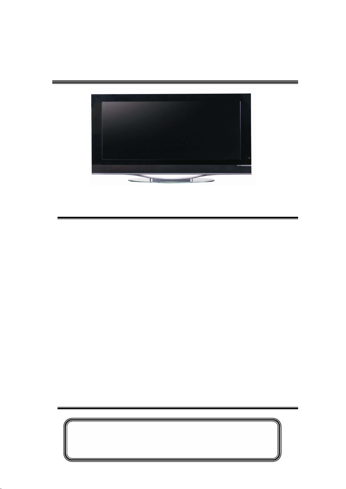
TCL
SERVICE MANUAL
LCD32M61S3-MS19
1. Chapter I specification………………………………………………………6
2. Chaper II Chassis Introduction…………………………………… ……10
Part I MCU working conditions……………………………………………12
Part II Reset section………………………………………………………… 12
Part III Tuner section…………………………………………………………13
Part IV Audio Amplifier and mute control………………………………… 14
Part V A v Out and Audio Amplifier…………………………………………14
Part VI HDMI and EDID introduction………………………………………15
Part VII HDCP Section………………………………………………………17
Part VIII EEPROM for Software……………………………………………18
Part IX Panel ON/OFF Control Section………………………………… …19
3. Chapter III IC Specifications …………………………………………………20
4. Chapter IV Alignment Procedure………………………………………………29
5. Chapter V Spare Parts List … ………………………………………………33
6. Chapter VIervice Guiding …………………………………………………50
Part I pictures of Chassis ………………………………………………………52
Part II Block of Diagram ………………………………………………………55
Part III Layout of Mainboard … ……………………………… … ………56
Part IV Scheme Diagram ………… ………………… …………… ………58
Part V Trouble shooting……………… ……… …………………… ………68
This manual is the latest at the time of printing, and does not
include the modification which may be made after the printing, by
the constant improvement of product
Page 2
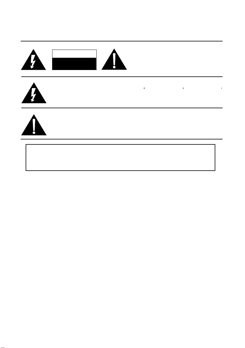
CAUTION:
Use of controls, adjustments or procedures other than those specified herein may result in
hazardous radiation exposure.
CAUTION: TO REDUCE THE RISK OF
CAUTION
RISK RISK OF OF ELECTRIELECTRICC
SHOCK SHOCK DO DO NOT NOT OPEN.OPEN.
The lighting flash with arrowhead symbol, with an equilateral triangle is intended to
alert the user to the presence of uninsulated voltage within the product s
enclosure that may be of sufficient magnitude to constitute a risk of electric shock to
the person.
The exclamation point within an equilateral triangle is intended to alert the user to the
presence of important operating and maintenance (servicing) instructions in the
literature accompanying the appliance.
ELECTRICAL SHOCK, DO NOT REMOVE
COVER (OR BACK). NO USER SERVICEABLE
PARTS INSIDE. REFER SERVICING TO
QUALIFIED SERVICE PERSONNEL.
dangerous
WARNING: TO REDUCE RISK OF FIRE OR ELECTRIC SHOCK, DO NOT
EXPOSE THIS APPLIANCE TO RAIN OR MOISTURE.
2
Page 3

IMPORTANT SAFETY INSTRUCTIONS
CAUTION:
Read all of these instructions. Save these instructions for later use. Follow all Warnings and
Instructions marked on the audio equipment.
1. Read Instructions- All the safety and operating instructions should be read before the product is operated.
2. Retain Instructions- The safety and operating instructions should be retained for future reference.
3. Heed Warnings- All warnings on the product and in the operating instructions should be adhered to.
4. Follow Instructions- All operating and use instructions should be followed.
FOR YOUR PERSONAL SAFETY
1. When the power cord or plug is damaged or frayed, unplug this television set from the wall outlet and refer servicing to
qualified service personnel.
2. Do not overload wall outlets and extension cords as this can result in fire or electric shock.
3. Do not allow anything to rest on or roll over the power cord, and do not place the TV where power cord is subject to
traffic or abuse. This may result in a shock or fire hazard.
4. Do not attempt to service this television set yourself as opening or removing covers may expose you to dangerous
voltage or other hazards. Refer all servicing to qualified service personnel.
5. Never push objects of any kind into this television set through cabinet slots as they may touch dangerous voltage
points or short out par ts that could result in a fire or electric shock. Never spill liquid of any kind on the television set.
6. If the television set has been dropped or the cabinet has been damaged, unplug this television set from the wall outlet
and refer servicing to qualified service personnel.
7. If liquid has been spilled into the television set, unplug this television set from the wall outlet and refer servicing to
qualified service personnel.
8. Do not subject your television set to impact of any kind. Be particularly careful not to damage the picture tube surface.
9. Unplug this television set from the wall outlet before cleaning. Do not use liquid cleaners or aerosol cleaners. Use a
damp cloth for cleaning.
10.1. Do not place this television set on an unstable cart, stand, or table. The television set may fall, causing serious injury
to a child or an adult, and serious damage to the appliance. Use only with a car t or stand recommended by the
manufacturer, or sold with the television set. Wall or shelf mounting should follow the manufacturer s instructions, and
should use a mounting kit approved by the manufacturer.
10.2. An appliance and car t combination should be moved with care. Quick stops, excessive force, and uneven surfaces
may cause the appliance and cart combination to overturn.
3
Page 4
PROTECTION AND LOCATION OF YOUR SET
11. Do not use this television set near water ... for example, near a bathtub, washbowl, kitchen sink, or laundry tub, in a
wet basement, or near a swimming pool, etc.
Never expose the set to rain or water. If the set has been exposed to rain or water, unplug the set from the wall
outlet and refer servicing to qualified service personnel.
12. Choose a place where light (artificial or sunlight) does not shine directly on the screen.
13. Avoid dusty places, since piling up of dust inside TV chassis may cause failure of the set when high humidity persists.
14. The set has slots, or openings in the cabinet for ventilation purposes, to provide reliable operation of the receiver, to
protect it from overheating. These openings must not be blocked or covered.
Never cover the slots or openings with cloth or other material.
Never block the bottom ventilation slots of the set by placing it on a bed, sofa, rug, etc.
Never place the set near or over a radiator or heat register.
Never place the set in enclosure, unless proper ventilation is provided.
a built-in
PROTECTION AND LOCATION OF YOUR SET
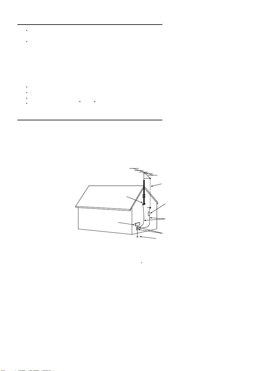
15.1. If an outside antenna is connected to the television set, be sure the antenna system is grounded so as to provide some
protection against voltage surges and built up static charges, Section 810 of the National Electrical Code, NFPA No.
70-1975, provides information with respect to proper grounding of the mast and supporting structure, grounding of the
lead-in wire to an antenna discharge unit, size of grounding conductors, location of antenna discharge unit, connection
to grounding electrode, and requirements for the grounding electrode.
EXAMPLE OF ANTENNA GROUNDING AS PER NATIONAL ELECTRICAL CODE INSTRUCTIONS
EXAMPLE OF ANTENNA GROUNDING AS PER
NATIONALELECTRICAL CODE
ANTENNA
LEAD- INWIRE
GROUND CLAMP
ELECTRIC SERVICE
EQUIPMENT
NEC-NATIONALELECTRICAL CODE
ANTENNA DISCHARGE
UNIT (NEC SECTION
810-20)
GROUNDING
CONDUCTORS
(NECSECTION 810-21)
GROUND CLAMPS
POWER SERVICE GROUNDING
ELECTRODE SYSTEM
(NEC ART 250. PARTH)
15.2. Note to CATV system installer : (Only for the television set with CATV reception)
This reminder is provided to call the CATV system attention to Article 820-40 of the NEC that provides
installer s
guidelines for proper grounding and, in part icular, specifies that the cable ground shall be connected to the grounding
system of the building, as close to the point of cable entry as practical.
16. An outside antenna system should not be located in the vicinity of overhead power lines or other electric lights or power
circuits, or where it can fall into such power lines or circuits. When installing an outside antenna system, extreme care
should be taken to keep from touching such power lines or circuits as contact with them might be fatal.
17. For added protection for this television set during a lightning storm, or when it is left unattended and unused for long
periods of time, unplug it from the wall outlet and disconnect the antenna. This will prevent damage due to lightning
and power-line surges.
4
Page 5

OPERATION OF YOUR SET
18.
This television set should be operated only from the type of power source indicated on the marking label. If you are not
sure of the type of power supply at your home, consult your television dealer or local power company. For television
sets designed to operate from battery power, refer to the operating instructions.
19. If the television set does not operate normally by following the operating instructions, unplug this television set from the
wall outlet and refer servicing to qualified service personnel. Adjust only those controls that are covered in the operating
instructions as improper adjustment of other controls may result in damage and will often require extensive work by a
qualified technician to restore the television set to normal operation.
20. When going on a holiday : If your television set is to remain unused for a period of time, for instance, when you go on
a holiday, turn the television set and unplug the television set from the wall outlet.
off
IF THE SET DOES NOT OPERATE PROPERLY
21. If you are unable to restore normal operation by following the detailed procedure in your operating instructions,
do not attempt any further adjustment. Unplug the set and call your dealer or service technician.
22. Whenever the television set is damaged or fails, or a distinct change in performance indicates a need for
service, unplug the set and have it checked by a professional service technician.
23. It is normal for some TV sets to make occasional snapping or popping sounds, particularly when being
turned on or off. If the snapping or popping is continuous or frequent, unplug the set and consult your
dealer or service technician.
FOR SERVICE AND MODIFICATION
24. Do not use attachments not recommended by the television set manufacturer as they may cause hazards.
25. When replacement parts are required, be sure the service technician has used replacement parts specified
by the manufacturer that have the same characteristics as the original part. Unauthorized substitutions
may result in fire, electric shock, or other hazards.
26. Upon completion of any service or repairs to the television set, ask the service technician to perform
routine safety checks to determine that the television is in safe operating condition.
5
Page 6
Specification
Items description
ID
Model L32M61S3
Model
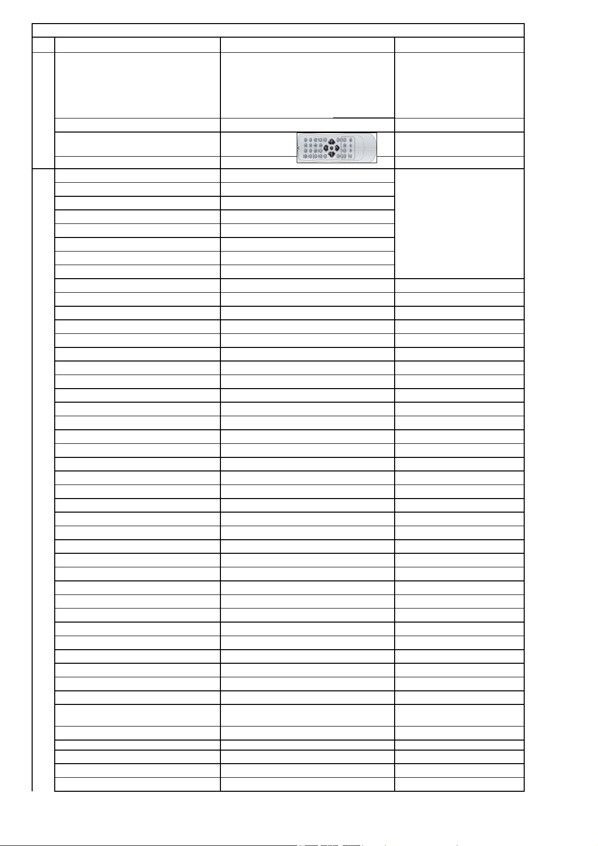
Remote Control Picture
RC TYPE Philips RC1113339
Basic Info.
+Panel Size(inch)
+Panel Supplier
+Aspect Ratio
+Chassis Name
+solution
+Market
+Certification
Panel Specification
+Model
+Pixel Pitch (vertical stripe RGB pixels)
+Resolution
+Brightness
+Contrast Ratio
+View Angle (H/V)
+Viewing Technology
+Response Time (Tr+Tf)
+Response Time (gray to gray)
+Back Lights (CCFLx)
+Panel Interface
+Color
+Life Time
Environmental Conditions
+Operation Temperature
+Storage Temperature
+Operation Humidity
+Storage Humidity
+Operation Air Pressure
General
+Storage Air Pressure
Power
+Power Supply
+Integrated Power Supply
+External Adapter
+Cord Type (Default)
+Power Consumption - TV ON
+Power Consumption - Standby
+LED indication - Power ON
+LED indication - STANDBY
+AC Switch
+Standby to Power ON
System
+Tuning - Max Programs
- Install Features Auto search and fine adjustment
- Technology PLL
- Indication Freq./CH
32"
CMO
16:9
MS19
MST9E19A
EM
CB
V320B1-L04
0.173mm (H) × 0.519mm (V)
1366X768
500 cd/m2
1200:1
176°/176°
TFT
6.5ms
16
LVDS
16.7M
MIN 50,000hrs
0-50°C
-20-60°C
90% RH MAX
10-90% RH
AC 100-240V,50/60Hz
YES
NO
VDE
130W
Less than 3W
BLUE
Red
Yes (Side BACK)
By CH+/- button on panel or ON-OFF/ CH+/- KEY
ON RC
200(0~199)
Remarks
Page 7
- Mode channel list
+TV Systems
+IF Freq.
+Freq. Bands
+Twin Tuner
+AV System
NTSC-M,PAL M,PAL N
45.75MHz
VHF-L VHF-H,UHF,Hyperband
---
PAL,NTSC
Picture-Processing(TV/Video)
+Scan
+Scaler Mode
+Comb Filter
+Black Strech, Blue Strech
+LTI, CTI
+PIP/POP - Type
+PIP/POP - Features
+Deinterlace
+Picture Effects
+Picture Enhancement
+Picture Noise Reduction
+Color Temperature
+Others
Please add other items referring to factual situation
Standard Progresive 60Hz
16:9, 4:3, zoom, cinerama
2D
Yes
Yes
NO
NO
Motion compensation
4 picture effects (Natural,Bright,Personal,Soft)
Cross-color supress(ccs) skin fresh
correction,Gama correction, Film mode
WEAK;medium;STRONG
normal;warm;cool
PC Compatibility
+VGA Input
+DVI Input
Picture
+HDMI Input
+DDC
VGA,SVGA,XGA,SXGA,WXGA@75Hz
XGA,up to SXGA@75Hz,720P,1080i
Yes
HDTV/SDTV Ready
+SDTV Input - YCbCr
+HDTV Input - YPbPr
+HDTV Input - DVI
+HDTV Input - VGA
(480p/480i,576p/576i)@60Hz
(720p,1080i,1080P)@50Hz/60Hz
(720p,1080i)@50Hz/60Hz
Build-in Data System
+Teletext Standard
+Teletext Language
+Teletext Pages
+Teletext Features
+CCD(Closed Caption)
+V-chip
+Macrovision
+CGMS
+HDCP
---
---
---
---
Yes
Yes
Yes
Yes
Sound Electric Performance
+RMS Power output(Internal)
+Speaker Max Power
2*12W
2*6W
Sound Effect
+Sound Processing
+DVSS(Dolby Virtual Surround Sound)
+AVC(Auto Volume Control)
+BBE
Sound
+SRS
BTSC
Yes
---
---
+Sound Features
+Sound Control
Please add other items referring to factual situation
Accessional Equipment
Stereo,News,MUSIC,Personal
AVC,MTS,SOUND MODE,BASS,TREBLE,
BALANCE
Page 8
+Card Reader
(
)
(
)
(
)
(
)
(
)
r
r
(
)
(
)
(
)
(
)
)
(
)
(
)
(
)
put(
(
)
(
)
(
)
)
(
)
(
)
t
p
(
)
)
(
)
(
)
(
)
(
)
r
)
(Type)
)
(
y
r
X
X
+DVD Combo
+Support USB Connection
+Built-in DTV Reception and System
Please add other items referring to factual situation
Operation Control
+Clock/Timer Function
+Lock
+OSD Features
+OSD Language
+OSD Main Menu
+Keyboard Control (Buttons on the panel)
Other Functions
+Remote Control
Other Functions
+Game
+Screen Protect
+Clear Screen
+Demo Functions
Please add other items referring to factual situation
Connectors Side
+AV Input - CVBS
Audio Input - R/L
Audio Input - Mono
+S-video
Audio Input - R/L
+Headphone Out - R/L
+USB Connecto
Connectors Rea
+AV Input - CVBS
Audio Input - R/L
+S-video
Audio Input - R/L
+Y,Pb,Pr Input
Audio Input - R/L
+Y,Cb,Cr Input
Audio Input - R/L
+VGA In
Headphone In R/L
Audio Input - R/L
+DVI Input
Audio Input - R/L
+HDMI Input
+SCART RGB+Y/C+CVBS In
+SCART RGB+Y/C+CVBS In/out
+SCART Y/C+CVBS In/ou
+SCART Y/C+CVBS In
+AV out
Audio output - R/L
Terminals
+Audio Output - R/L
+Audio Output - R/L
+Headphone Out - R/L
+Audio Output - Woofe
+Control/Signal Socket (for MFB)
+S/W Updating Socket
+RF - Terr.Antenna in
+ITV Smart Port
+I-Link
+IR Blaster Jack
+Other Function Extended Interfaces
+Power In Cinch
ut-CVBS
1394) Capacit
Connectors Front
+AV Input - CVBS (RCA)
Audio Input - R/L (RCA) ---
Audio Input - Mono (RCA) ---
+Headphone Out - R/L (Φ3.5mm)
+USB Connecto
Connectors Top
Please add other items referring to factual situation
Connectors Bottom
Please add other items referring to factual situation
Configuration
+Cabinet Name
RCA
RGB)
RCA
RCA
RCA
RCA
Φ3.5mm
RCA
RCA
RCA
RCA
RCA
RCA
D-SUB15
Φ3.5mm
RCA
RCA
full
RCA
RCA
RCA
Line
Φ3.5mm
(RCA
---
---
---
---
24h Timer;TURN ON/OFFf;Sleep timer
OSD position adjustable,
English,French,Spanish,Portuguese
Picture,Sound,PAR.CONTROL,Preferences,Setup
,TIMER
Source,Menu,CH+,CH-,Vol+,Vol-,
ON-OFF,MENU,INPUT,CH+/-,VOL+/,SOUND,PRESET,INFO,FAVORITE,etc,.
---
---
---
---
---
---
---
2
2
1
Share with AV1
1 (component
1
Share with Y,Pb,Pr
Share with Y,Pb,Pr Audio input
1
1(Share with Y,Pb,Pr Audio input
1
---
---
---
--1 (Only for TV/AV source
1
1
---
--Share with VGA SOCKET
75ohm(F TYPE
---
---
---
--AC code in
---
---
---
X
X
M61
Page 9
+Features
g
g
)
)
)
(mm)
)
)
t
x
t
+Speaker Assemble Mode
+Speaker Grille
+Front Cabinet - Material and Color
+Rear Cabinet - Material and Color
+Keyboard Position
+Tuner Detachable
Flat (no arc)
Integrated
original holes in F.CAB
HIPS Black A6881
HIPS Black A8252
Middle on top of the front panel
No
Artwork
En
+Operation Manual Language
o Features (Front panel
+Lo
+Dimension - with Base Stand (L*H*D
- without Base Stand (L*H*D)
+Dimension - packaged (L*H*D
+Net Weight
+Gross Weight
+Container Loading - 20 fee
- 40 feet 234sets
- 40 feet high 234sets
lish
stamp
813*613*219(mm
813*562*100
986*731*358(mm
16.5kg
20Kg
111sets
Wall Mount
+Type
+Features
+Packaging Method
+Dimension - packaged (L*H*D)
+Net Weight and Gross Weight
WMB230 (optional)
fixed
Separated
265*168*44(mm)
Net Weight: 0.2kg ; Gross Weight:0.5 Kg
Speaker Bo
+Fixing Method
+Features
+Packaging Method
+Dimension - packaged (L*H*D)
+Dimension - unpackaged (L*H*D)
+Net Weight and Gross Weight
Multi-function Box
+Packaging Method
+Dimension - unpackaged (L*H*D)
+Dimension - packaged (L*H*D)
+Net Weight and Gross Weight
---
---
---
---
---
---
---
---
---
---
---
Base Stand
+Features
+Packaging Method
+Dimension - packaged (L*H*D)
+Dimension - unpackaged (L*H*D)
Configuration&Artwork
+Net Weight and Gross Weight
+Container Loading - 20 fee
- 40 feet no
- 40 feet high no
Integrated
no
no
Net Weight:2 Kg ; Gross Weight: 2Kg
no
Accessories
+Operation Manual
+Service Manual
+Warranty Card
+Schematic Diagram
+Remote Control
+Battery (number and type) Yes (2×AA,1.5V)
+Speakers Box(external)
+Wall Mount
+Wireless Headphone (external)
+RF Cable
+Power Cord
+DVI Cable
+VGA Cable
+HDMI Cable
+Control/Signal Cable (Panel to MFB)
+AV Cable
+Component Video Cable
+Audio Cable
Please add other items referring to factual situation
Yes
---
---
---
Yes
---
optional
YES
: ,
Page 10

Chapter II Chassis Introduction
LCD32E62S3/LCDM61S3/LCDM71S3 adopted Mstar integrated 1-chipset solution MS19
(MST9E19A).It has characteristics as following,
¾ MStarACE-3 (3rd Generation Advanced Color Engine) Automatic Picture/Color
Processor:
. Brilliant and fresh color
. Intensified contrast and details
. Vivid skin tone
. Sharp edge
. Enhanced depth of field perception
. Accurate and independent color control
¾ 2D Comb filter
¾ Progressive Scan
¾ Digital Noise Reduction
¾ Film Mode (3:2 pull down)
¾ Gamma Correction
¾ 4 Picture Effects (Natural,Standard,Bright,Soft)
¾ Variable Aspect Ratio (16:9,4:3,Cinerama,Zoom)
¾ HDTV-Ready (1080i;720p)@50Hz/60Hz
¾ HDMI/VGA Input up to SXGA@75Hz
¾ V-Chip
¾ CCD
¾ Sleep Timer,24h timer turn on/off
¾ MTS Stereo (BTSC-SAP)
¾ 4 Mode Sound Presets (Standard; News; Music; Personal)
¾ Sound Control: Treble, Bass, Balance, AVL etc.
¾ HDMI (HDCP) input ×1 , (V1.1)
¾ RF input (NTSC-M,PAL-M/N) ×1
¾ HDTV input (Component) ×1
¾ AV i nput ×2
¾ S-Video input ×1
¾ VGA input ×1
¾ AV output ×1
¾ Headphone output×1
Chassis MS19 circuitries include: tuner, decoder and scanner, audio amplifier, remote control
receive, key input and power supply unit and so on. It adopted ICs as following, MST9E19A-LF
208PI, ISL8105IBZ, TDA7266 , TDA1308T/N2, TL431ACLP, M24C32, KD1084A-18.
I. Video signal input processing circuit.
Radio frequency signal from antenna or cable input tuner, after it processed, Pin17 of tuner output
video signal, then input Pin49/50 of U8(MST9E19A).
II. AV signal input processing circuit.
Page 11

AV1/AV3 through socket P14 input Pin45/Pin47 of U8, S-video input through socket P15 input
Pin42/Pin43/Pin44 of U8. YCbCr Video Signal input through socket P16 input.
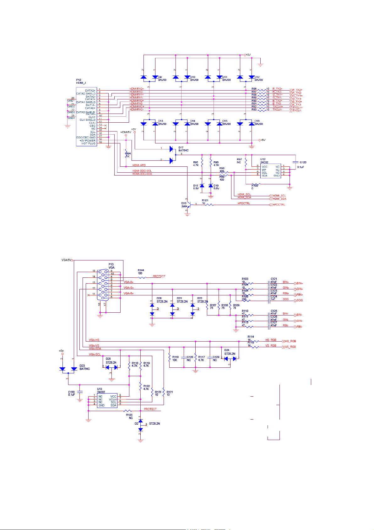
III.HDMI video signal input through socket P12 input Pin1-Pin15 of U8.
IV.VGA input through socket P13 input Pin16-Pin28 of U8.
V. Audio signal input, the audio signal through antenna process and output from Pin7 of Tuner
and input Pin54/Pin55 of U8.The AV1’s audio signal input Pin63/Pin64 of U8,AV2’s audio signal
input Pin66/Pin67 of U8; AV3’s audio signal input Pin69 and Pin69 of U8.
All channels audio signal through inside circuitry process, output from Pin74/Pin75 of U8, send to
audio amplifier U19( TDA7266SA) processing and driver speaker phonat in g.
Page 12
Representative Circuitry Introduction
Part I Mcu Working Conditions
I. power supply showing as following figure,
II. reset circuitry working normal.
III. Crystal working normal
IV. SCL and SDA working normal and so on.
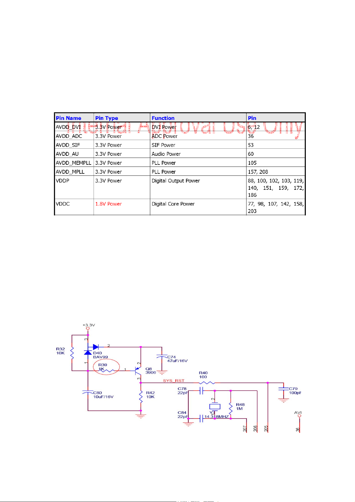
Part II. Reset Section
Each time turn on the TV, after power supply loading, the reset circuitry is working, Pin205 of
U8 is high level durative about 40ms, then finished the TV reset. It is low level under normal
situation. While the 3.3V voltage is loading, charge on C74 and C80, due to the resistance of D40
is smaller than R32, so the voltage on C74 will higher than C80, Q8 turnon, the current passes
Q8,Pin205 of U8 get high level. As the voltage charge on C80 fully, Q8 cut-off, finished the TV
reset.
Page 13
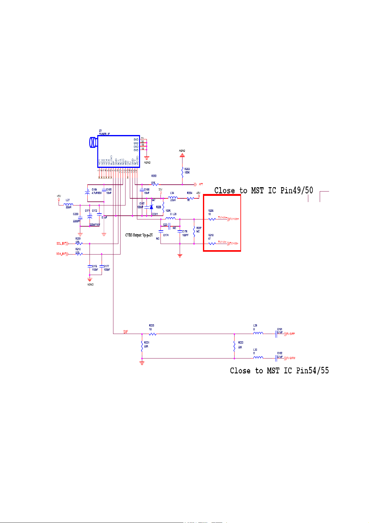
Part III. Tuner Section
Tuner receives the RF signal, and after the circuitry inside it deal with, and get the CVBS signal
sends to Pin49/50 of MST IC. The another signal path is SIF signal out from Pin7 of Tuner and
sends to Pin 54/55 of MST IC. The detail signal following process please refer to circuitry
diagram as following,
Page 14
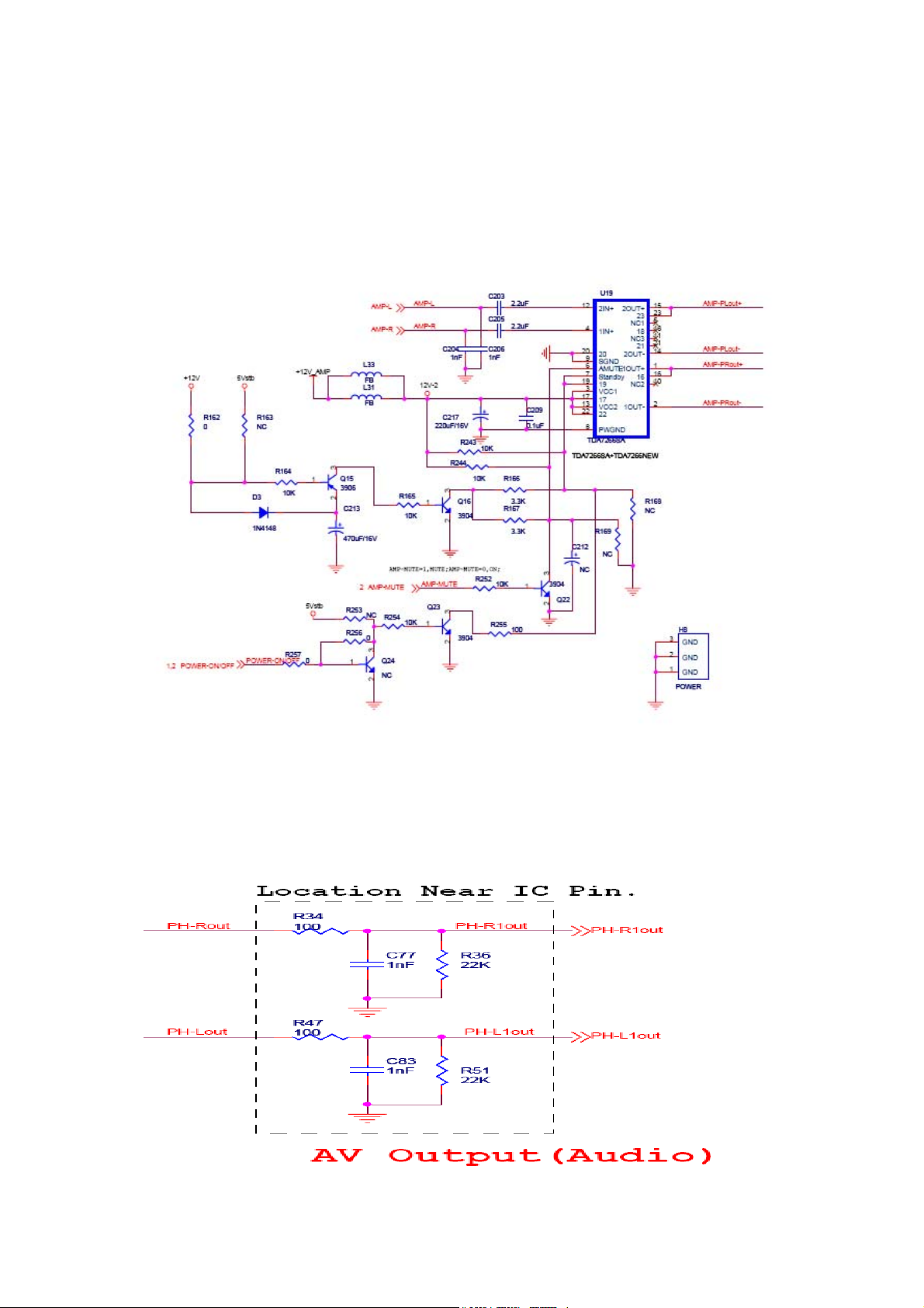
Part IV Audio Amplifier and Mute Control
The audio signal after MST IC decoder and get out from Pin74/75 of MST IC, and through
integral circuitry (R33,R38,C76 and R45,R50,C82) send to Pin4/12 of audio power amplifier
U19 to drive speaker.
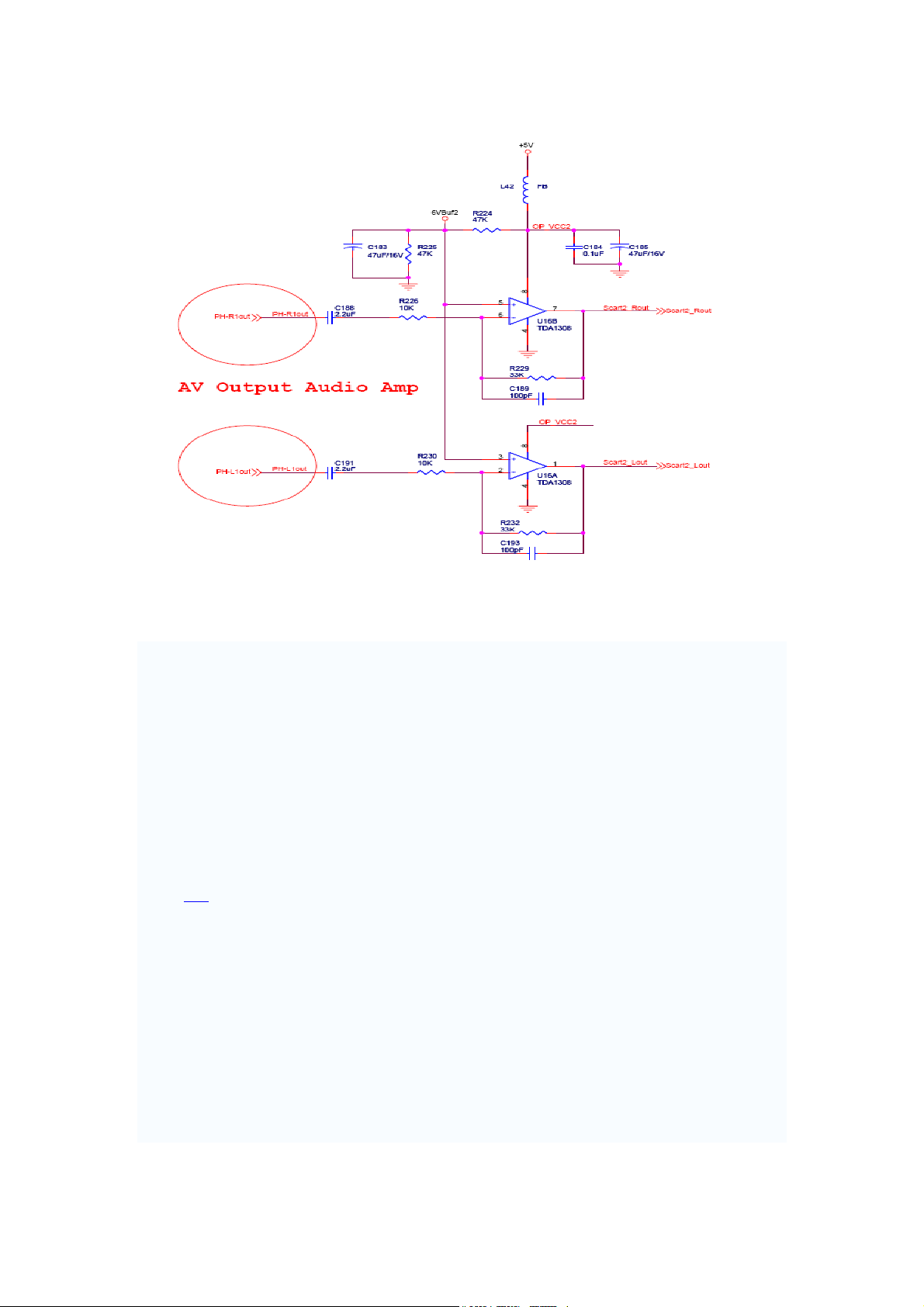
Part V A V Output Audio Amplifier Section
The phone audio signal output from Pin71/Pin 71,through the integral circuitry R34/R36/C37 and
R47/R51/C83 send to U16 and output from P17.
Page 15
Part VI HDMI EDID Introduction
Extended display identification data (EDID) is a data structure provided by a
computer display to describe its capabilities to a graphics card. It is what enables
a modern personal computer to know what kind of monitor is connected. EDID is defined
by a standard published by the Video Electronics Standards Association (VESA). The
EDID includes manufacturer name, product type, phosphor or filter type, timings
supported by the display, display size, luminance data and (for digital displays
only) pixel mapping data.
The channel for transmitting the EDID from the display to the graphics card is usually
the I2C bus. The combination of EDID and I²C is called the Display Data Channel version
2, or DDC2. The 2 distinguishes it from VESA's original DDC, which used a different
serial format.
Before DDC and EDID were defined, there was no standard way for a graphics card to
know what kind of display device it was connected to. Some VGA connectors in personal
computers provided a basic form of identification by connecting one, two or three
pins to ground, but this coding was not standardized.
The EDID is often stored in the monitor in a memory device called a serial PROM
(programmable read-only memory) or EEPROM (electrically erasable PROM) that is
compatible with the I²C bus.
Page 16
VGA EDID OR DDC
Page 17
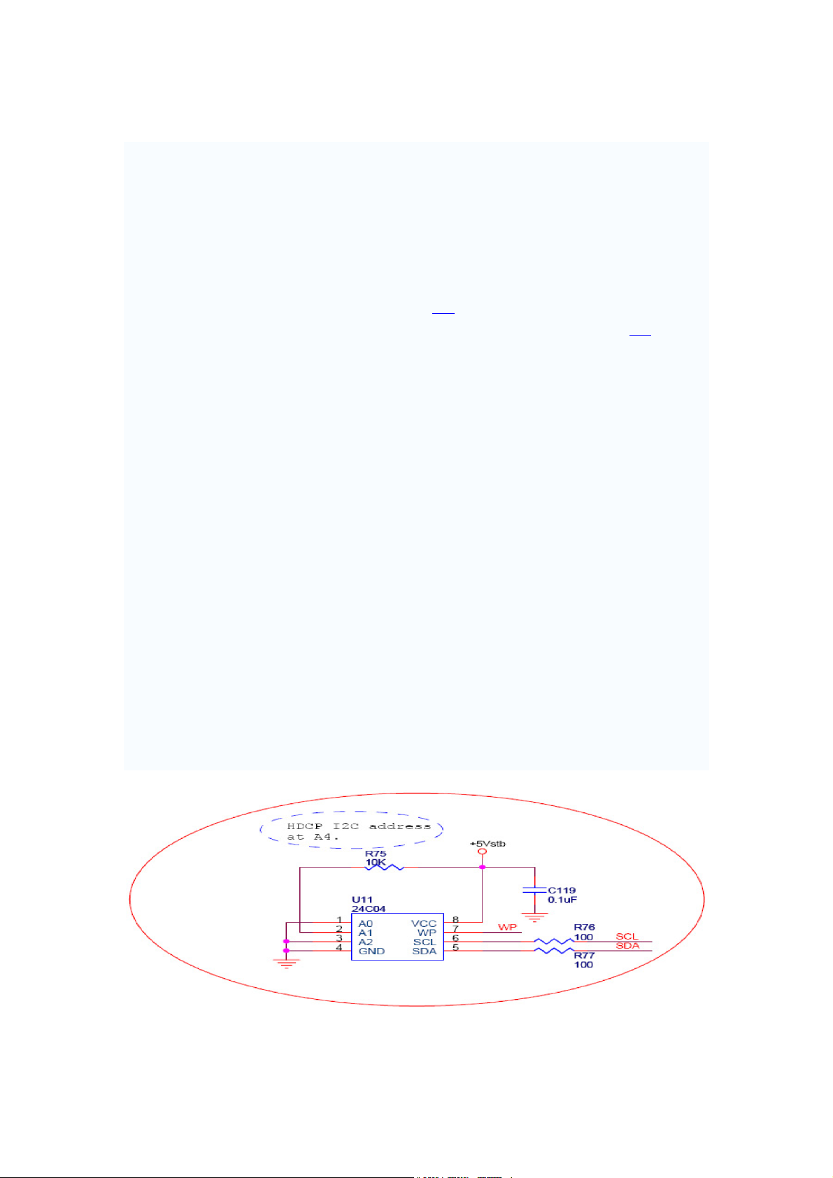
PART VII HDCP Section
High-bandwidth Digital Content Protection (HDCP) is a form of Digital Rights
Management (DRM) developed by Intel Corporation to control digital audio and video
content as it travels across Digital Visual Interface (DVI) or High-Definition
Multimedia Interface (HDMI) connections. The specification is proprietary, and
creating an implementation of HDCP requires a license .HDCP is licensed by Digital
Content Protection, a subsidiary of Intel. In addition to paying fees, licensees
agree to limit the capabilities of their products. For example, high-definition
digital video content must be restricted to DVD quality on non-HDCP compliant video
outputs when requested by the source. DVD-Audio content is restricted to DAT quality
on non-HDCP digital audio outputs (analog audio outputs have no quality limits).
Licensees cannot allow their devices to make copies of content, and must design their
products in ways that "effectively frustrate attempts to defeat the content
protection requirements."
Each HDCP capable device has a unique set of keys; there are 40 keys, each 56 bits
long. These keys are confidential and failure to keep them secret may be seen as
a violation of the license agreement. For each set of keys a special key called a
KSV (Key Selection Vector) is created. Each KSV has exactly 20 bits set to 0 and
20 bits set to 1.
During the authentication process, both parties exchange their KSVs. Then
each device adds (without overflow) its own secret keys together according
to a KSV received from another device. If a particular bit in the vector
is set to 1, then the corresponding secret key is used in the addition,
otherwise it is ignored. Keys and KSVs are generated in such a way that
during this process both devices get the same 56 bit number as a result.
That number is later used in the encryption process.As result that, this
chassis adopts 24C04 to storage KSV and license makes digital signal
resource output.
Page 18
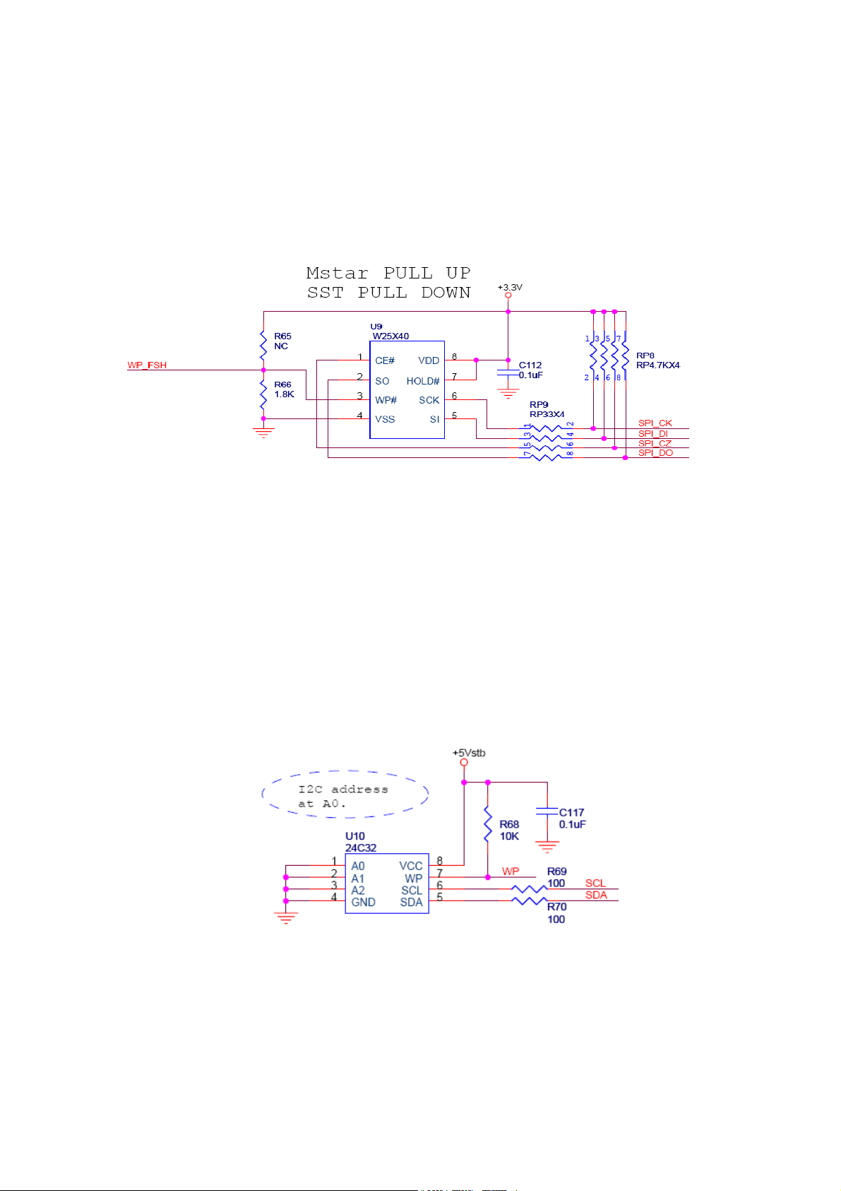
PART VIII EEPROM for Software
It adopts Winbond company’s W25X40 flash which has 4M-bit/526 bytes and 2048pages.It is
used for storage the main system software. The devices operate on a single 2.7V to 3.6V power
supply with current consumption as low as 5mA active and 1uA for power-down.。
EEPROM for User Information
2
It adopts I
C compatible electrically erasable programmable memory (EEPROM) devices are
organized as 4096x8 bits(32k).This is a two-wire series interface that uses a bi-directional data bus
and serial clock. It is used for storage user’s information, such as channel search and timer on and
off, and picture standard and other information what user’s easy to change by local key board and
remote control.
Page 19
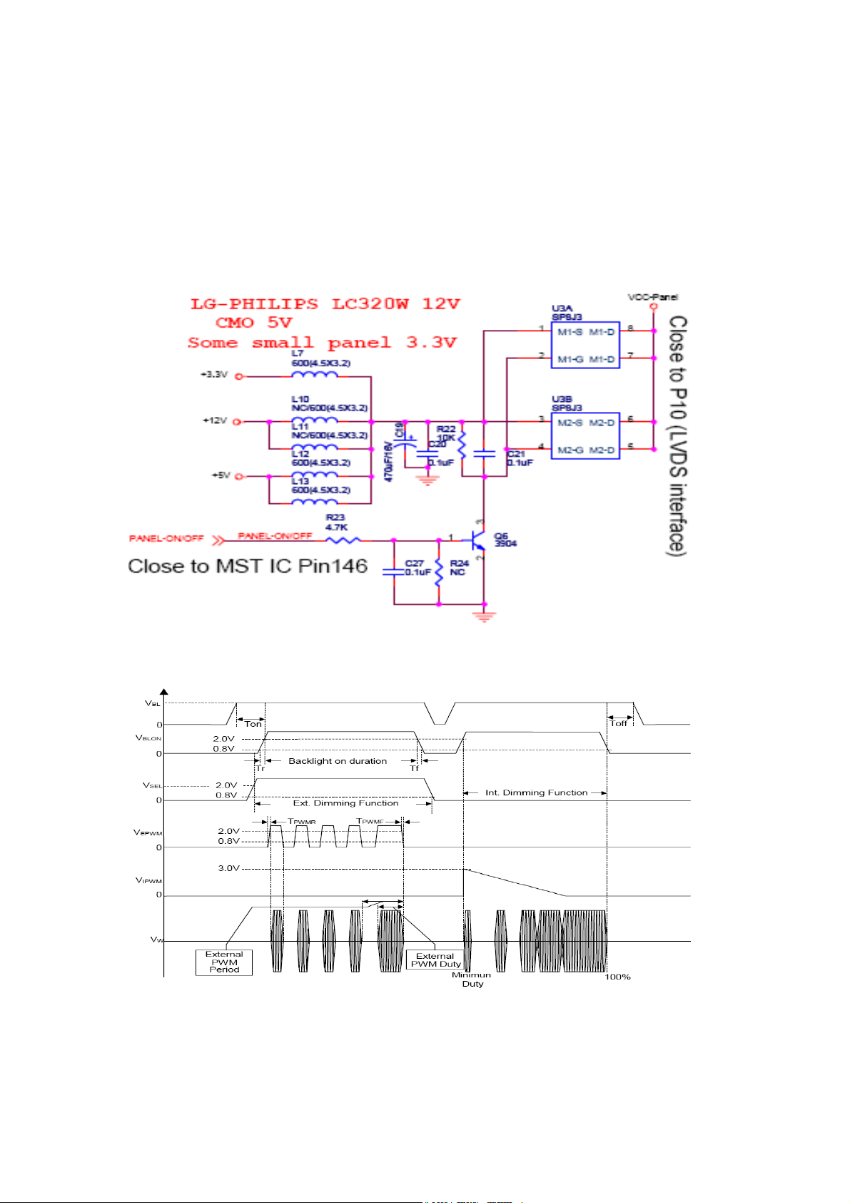
PART IX Panel ON/OFF Control Section
While the TV is turn on, the TV is standby situation. While command turn on is send out, 5v
voltage will through regulator and equal get 3.3V voltage or 1.8V voltage supply for U8. After
reset and crystal Y1 working, the main system software will be loaded, the panel –ON/OFF
command will be sent out, makes the dual-MOSFET U3 turn on and send 5V/12V/3.3V voltage to
the panel.
The following figure is showing the power sequence and control signal timing.
Page 20

Chapter III IC Sepecifications
Part I Specification of MST9E19A
Part II Specification of TDA7266
Page 21

SXGA/WXGA+ LCD TV Controller with Video Decoder & 10-bit Dual LVDS Transmitter
FEATURES
Ÿ Single display LCD TV controller with PC &
multimedia display functions
Ÿ Input supports up to SXGA & 1080P
Ÿ Panel supports up to
SXGA(1280x1024)/WXGA+(1440x900)
Ÿ Multi-Standard TV decoder with 2-D comb filter
Ÿ Multi-Standard TV sound demodulator and decoder
Ÿ Triple-ADC for TV and RGB/YpbPr
Ÿ Integrated DVI/HDCP/HDMI compliant receiver
Ÿ High-quality scaling engine
Ÿ 3-D video de-interlacer and video noise reduction
for SDTV input
Ÿ 2-D video de-interlacer and video noise reduction
for HDTV input
Ÿ MStarACE-3
Ÿ Embedded On-screen display controller (OSD)
engine
Ÿ Built-in MCU supports PWM & GPIO
Ÿ Built-in 8/10-bit dual-link LVDS transmitter
Ÿ 5 Volt tolerant inputs
Ÿ Low EMI and power saving features
Ÿ 208-pin PQFP
n NTSC/PAL/SECAM Video Decoder
Ÿ Supports NTSC, NTSC-4.43, PAL
(B,D,G,H,M,N,I,Nc), and SECAM
Ÿ Automatic TV standard detection
Ÿ Adaptive 2-D comb filter for NTSC/PAL
Ÿ 8 configurable CVBS & Y/C S-video inputs
Ÿ Supports Teletext level-1.5, WSS, VPS,
Closed-caption, and V-chip
Ÿ Macrovision detection
Ÿ CVBS video output
n Multi-Standard TV Sound Decoder
Ÿ Supports BTSC/NICAM/A2/EIA-J demodulation
and decoding
Ÿ FM stereo & SAP demodulation
Ÿ L/Rx4 and SIF audio input
Ÿ L/R loudspeaker and line output
Ÿ Supports sub-woofer output
Ÿ Built-in audio output DAC’s
Ÿ Audio processing for loudspeaker channel,
including volume, balance, mute, tone, EQ, and
virtual stereo/surround
n Digital Audio Interface
2
Ÿ I
S digital audio output
Ÿ S/PDIF digital audio output
Ÿ Programmable delay for audio/video
synchronization
n Analog RGB Compliant Input Ports
Ÿ Two analog ports support up to 150MHz
Ÿ Supports PC RGB input up to SXGA@75Hz
Ÿ Fast blanking and function selection switch
support full SCART functions
picture/color processing engine
MST9E19A
Preliminary Data Sheet Version 0.1
Ÿ Supports HDTV RGB/YPbPr/YCbCr up to
1080P
Ÿ Supports Composite Sync and SOG
(Sync-on-Green) separator
Ÿ Automatic color calibration
n DVI/HDCP/HDMI Compliant Input Port
Ÿ Operates up to 150 MHz (up to SXGA @75Hz)
Ÿ Single link on-chip DVI 1.0 compliant receiver
Ÿ High-bandwidth Digital Content Protection
(HDCP) 1.1 compliant receiver
Ÿ High Definition Multimedia Interface (HDMI)
1.2 compliant receiver
Ÿ Long-cable tolerant robust receiving
Ÿ Support HDTV up to 1080P
n Auto-Configuration/Auto-Detection
Ÿ Auto input signal format and mode detection
Ÿ Auto-tuning function including phasing,
positioning, offset, gain, and jitter detection
Ÿ Sync Detection for H/V Sync
n High-Performance Scaling Engine
Ÿ Fully Programmable shrink/zoom capabilities
Ÿ Nonlinear video scaling supports various modes
including Panorama
Ÿ Supports keystone correction for projectors
n Video Processing & Conversion
Ÿ 3-D motion adaptive video de-interlacer for
SDTV
Ÿ 2-D video de-interlacer for HDTV
Ÿ Edge-oriented adaptive algorithm for smooth
low-angle edges
Ÿ Automatic 3:2 pull-down & 2:2 pull-down
detection and recovery
Ÿ MStar 3
rd
Generation Advanced Color Engine
(MStarACE-3) automatic picture enhancement
gives:
Ÿ Brilliant and fresh color
Ÿ Intensified contrast and details
Ÿ Vivid skin tone
Ÿ Sharp edge
Ÿ Enhanced depth of field perception
Ÿ Accurate and independent color control
Ÿ sRGB compliance allows end-user to experience
the same colors as viewed on CRTs and other
displays
Ÿ Programmable 12-bit RGB gamma CLUT
Ÿ 3-D video noise reduction for SDTV and 2-D
video noise reduction for HDTV
Ÿ Frame rate conversion
n On-Screen OSD Controller
Ÿ 16/256 color palette
Ÿ 256/512 1-bit/pixel font
Ÿ 128/256 4-bit/pixel font
Ÿ Supports texture function
Version 0.1 - 1 - 5/19/2006
Copyright © 2006 MStar Semiconductor, Inc. All rights reserved.
Page 22

MST9E19A
SXGA/WXGA+ LCD TV Controller with Video Decoder & 10-bit Dual LVDS Transmitter
Preliminary Data Sheet Version 0.1
Ÿ Supports 4K attribute/code
Ÿ Horizontal and vertical stretch of OSD menus
Ÿ Pattern generator for production test
Ÿ Supports OSD MUX and alpha blending
capability
Ÿ Supports blinking and scrolling for closed
caption applications
n LVDS/TTL Panel Interface
Ÿ Supports 8/10-bit dual link LVDS up to
SXGA(1280x1024)/WXGA+(1440x900)
Ÿ Supports 8-bit single TTL panel
Ÿ Supports 2 data output formats: Thine & TI data
mappings
Ÿ Compatible with TIA/EIA
Ÿ With 6/8 bits options
Ÿ Reduced swing for LVDS for low EMI
Ÿ Supports flexible spread spectrum frequency
with 360Hz~11.8MHz and up to 25% modulation
n Integrated Micro Controller
Ÿ Embedded 8032 micro controller
Ÿ Configurable PWM’s and GPIO’s
Ÿ Low-speed ADC inputs for system control
Ÿ SPI bus for external flash
Ÿ Supports external MCU option controlled
through 4-wire double-data-rate direct MCU bus
or 8-bit direct MCU bus
n External Connection/Component
Ÿ Step-down PWM power control
Ÿ All system clocks synthesized from a single
external clock
GENERAL DESCRIPTION
The MST9E19A is a high performance and fully integrated IC for multi-function LCD monitor/TV with resolutions
up to SXGA(1280x1024)/WXGA+(1440x900). It is configured with an integrated triple-ADC/PLL, an integrated
DVI/HDCP/HDMI receiver, a multi-standard TV video and audio decoder, a video de-interlacer, a scaling engine, the
MStarACE-3 color engine, an on-screen display controller, an 8-bit MCU, and a built-in output panel interface. To
further reduce system costs, the MST9E19A also integrates intelligent power management control capability for
green-mode requirements and spread-spectrum support for EMI management.
Version 0.1 - 2 - 5/19/2006
Copyright © 2006 MStar Semiconductor, Inc. All rights reserved.
Page 23

SXGA/WXGA+ LCD TV Controller with Video Decoder & 10-bit Dual LVDS Transmitter
PIN DIAGRAM (MST9E19A)
MST9E19A
Preliminary Data Sheet Version 0.1
RXCKN
RXCKP
GND
RX0N
RX0P
AVDD_DVI
RX1N
RX1P
GND
RX2N
RX2P
AVDD_DVI
REXT
DDCD_DA
DDCD_CK
HSYNC1
VSYNC1
RMID
VCLAMP
REFP
REFM
BIN1P
BIN1M
SOGIN1
GIN1P
GIN1M
RIN1P
RIN1M
BIN0M
BIN0P
GIN0M
GIN0P
SOGIN0
RIN0M
RIN0P
AVDD_ADC
GND
HSYNC0
VSYNC0
VCOM2
CVBS3
CVBS2
CVBS1
VCOM1
CVBS0
VCOM0
CVBSOUT
GND
1
2
3
4
5
6
7
8
9
10
11
12
13
14
15
16
17
18
19
20
21
22
23
24
25
26
27
28
29
30
31
32
33
34
35
36
37
38
39
40
C1
41
Y1
42
C0
43
Y0
44
45
46
47
48
49
50
51
52
Pin 1
156
PWM3
155
PWM2
154
DIGO[9]
153
DIGO[8]
152
GND
151
VDDP
150
DIGO[7]
149
DIGO[6]
148
DIGO[5]
147
DIGO[4]
146
DIGO[3]
145
DIGO[2]
144
DIGO[1]
143
DIGO[0]
142
VDDC
141
GND
140
VDDP
139
PWM_SENSE
138
PWM_DRV
137
PWM_FB
136
IRIN
135
INT
134
DDCA_CK
133
DDCA_DA
132
DDCR_CK
131
DDCR_DA
130
PWM1
129
PWM0
128
SAR3
127
SAR2
126
SAR1
125
SAR0
124
SDO
123
CSZ
122
SDI
121
SCK
120
GND
119
VDDP
118
ALE
117
RDZ
116
WRZ
115
AD[7]
114
AD[6]
113
AD[5]
112
AD[4]
111
AD[3]
110
AD[2]
109
AD[1]
108
AD[0]
107
VDDC
106
GND
105
AVDD_MEMPLL
Version 0.1 - 3 - 5/19/2006
Copyright © 2006 MStar Semiconductor, Inc. All rights reserved.
Page 24

Page 25

Page 26
Page 27

Page 28

Page 29

TCL Multimedia R&D Center File number:
Chapter IV Alignment of MS19
Alignment
1
Model: L32M61S3/L32E62S3/L32M71S3 (MS19)
Edition:V1.1
Prepared by: Tang Zhongzi Date: May30,2007
Approved by: Date:
Page 30
TCL Multimedia R&D Center File number:
2
I. Brief Introduction
This Chassis adopts Taiwan semiconductor plant MSTar’s integrative chip MST9E19A.It is a high
performance and fully integrated IC for multi-function LCD monitor/TV with resolutions up to
SXGA(1280x1024)/WXGA+(1440x900).It is con figured with an integrated triple ADC-PLL, a n
integrated DVI/HDCP/HDMI receive a multi-standard TV video and audio decoder, a video
de-interlacer, a scaling engine, the MStarACE-3 color engine an on-screen display controller, an
8-bit MCU, and a built-in output panel interface. To further reduce system costs, the MST9E19A
also integrates intelligent power management control capability for green-mode requirement and
spread-spectrum support for EMI management. Therefore, MS19 is a high cost performance
Chassis.
Modes L32M61S3/L32E62SE/L32M71S3 just different in frame, their chassis includes ha rdware
and software almost are same. To match the frame, just key board and remote control receive
board have a little difference. Beside, the three modes TV support NTSC-M, PAL M and PAL N.
So that, the following alignment procedure adapt to the three modes above said.
II. How to enter factory mode (service menu, service mdoe)
Method one, press MENU, input “1”,”9”,”5”,”0” in 3 seconds.
Method two, press “GO BACK” key directly. (Remark: it is must under conditions of, in factory
mode, enter PRODUCTING, FACTORY HOT KEY set as ON.)
III. Factory menu explain
Enter factory menu, press the remote control’s UP, DOWN, LEFT, RIGHT key set or adjustment,
press MENU key return parent menu, press MENU OR CLEAR KEY exit factory menu.
Options menu Function explain function
Source Choose this item, press LEFT and RIGHT key can switch
OK
the signal source.
ADC ADJ Only source as HDTV or PC, can enter and adju st. OK
WB Enter white balance adjustment. OK
source Sources switch OK
Color
TEMP
There are three color temperatures:
OK
NORMAL,WARM,COOL
White R Channel R gain. It can adjust by auto or manual. OK
White G Channel G gain. It can adjust by auto or manual. OK
White B Channel B gain. It can adjust by auto or manual. OK
Black R Channel R excursion. It can adjust by auto or manual. OK
Black G Channel G excursion. It can adjust by auto or manual. OK
Black B Channel B excursion. It can adjust by auto or manual. OK
VOL
CURVE
Sound curve adjustment, X0,X1,X2,X3,X4 separate stand
for volume in user menu 0,30,50,80,100.This item test OK
in factory, user do not adjust it.
Picture
curve
Picture analog curve adjustment.X0,X1,X2, X3, X4 are
separate stand for picture menu 0,30,50,80, 100. This item is
adjust OK in factory, user do not adjust it again.
CON Contrast curve OK
BRI Brightness curve OK
Page 31

TCL Multimedia R&D Center File number:
3
SAT. Saturation curve OK
SHARP Sharpness curve OK
Light Back light curve OK
Picture
mode
This function set four picture modes in factory
menu(soft,natural,bright, personal) their simulate volume
can adjust, but it is adjust well while designing. It can be
fine adjust in special case.
Producting Items must be adjusted in factory producing OK
Factory
hot key
Shortcut key for enter factory mode. If it is set as ON, can
enter factory menu through press ‘GO BACK’ on remote
OK
control. Must set as OFF before TV go out of plant.
Warm
status
Aging mode. If this item set as ON, while there is no signal
input, TV should be snow dots, not blue screen. When TV
OK
need aging, please set as ON, the default is OFF, please set
as OFF before go out of plant.
EEPROM
init
Initial EEPROM. The first start up must initial EEPROM
after the TV is finish assembly. Press LEFT or RIGHT key
and wait for about 7 seconds, will display OK on screen, it
says that finished the initial. Please turn off the TV then
restart up and adjust the other items.
Structure Frame(mode) choose. This chassis compatible with several
OK
modes. Switch this item can choose mode, nowadays there
are E62(L32E62S3) and M61-M71(L32M61S3/L32M71S3)
can be chose, while producing, must confirm the mode first,
then switch it right. It goes into effect after turn off the TV.
Shop
content
Some out factory set, please obey the default value, without
customer special necessary.
OK
Volume Default value 30 OK
Picture
Default natural OK
mode
Sound
Default STEREO OK
mode
TV
Default channel is 1 OK
channel
Language Default English OK
Color
Option item, normal, warm, cool OK
Tone
SET UP The process of start up setting, default is LAST OK
Power
mode
Last, makes the TV memory last turn off TV’s situation. For
example, if plug off the AC power cord to turn off the TV, it
OK
will be turn on while plug in the power cord; if standby the
TV last time, it should be turn on be manual.
Power
mode STB
STB(standby), TV insist as standby situation while power
on, need manual turn it on.
OK
Page 32

TCL Multimedia R&D Center File number:
4
Power on ON, it says that TV will turn on while power on. While
OK
aging, please set as ON.
Shop init
DO
Initial. Press left or right key to initial. While there is OK
display on the screen, finished initial. Please initial the TV
OK
while it will out of plant.
IV. Aging
While TV need aging, pleas enter factory mode, set the WARM UP STATUS in producting as ON,
then set power mode as ON in set up menu. If TV need standby aging, please set power mode as
STB.
V. Producing Items adjustment.
1. ADC correct
This chassis can ADC correct when input YPBPR or PC signal resource. Enter factory mode,
switch the source as YPBPR or PC, input 100% color bar signal, enter ADC ADJ item, choose
AUTOTUNE item, press right key on remote control to start auto correct, when screen display OK
7 seconds later, it shows that ADC correct success. Then exit menu.
Remark: Before white balance adjustment, must do ADC correct OK in YPBPR and PC signal
input.
2. White balance adjustment.
Normal, warm and cool three situations’s white balance color temperature value must obey the
enterprise standard. Before adjust the white ba lance, please co nfir m if finish ed ADC co rrect unde r
YPBPR and PC sources, in addition, the picture mode must be normal.
This chassis white balance adjustment must be adjusted in three signal sources.
(1)AV/TV/S-Video’s white balance adjust under AV signal source input. Signal should be
NTSC-M eight-grey bar signal.
(2)YPBPR and HDMI white balance adjust under YPBPR signal source input. Signal must be
16-grey bar signal.
(3)PC white balance adjustment must be under PC signal input. The signal should be 16 grey bar
signal.
Factory producing white balance adjustment according to the software interface agreement and
working guide, setting relevant offsets to operate.
If it need human adjustment, please enter factory menu adjust WB items.
3. leave factory setting.
Leave factory setting items have been listed in factory menu. Please set each character according
to customers requirement. Or obey the default value. Before TV leave factory, please do “SHOP
INIT DO”. Operate method is press left or right key on remote control to initial it. While OK
display on screen, it finished the initial. Then turn TV off just OK..
Page 33

Chapter V Spare Parts List
H3-HM61AS3-SM00C B L32M61S3/MS19
parent child description BOM text
H3-HM61AS3-SM00C 08-LON37A-PW1W ASS'Y - POWER BD
08-LON37A-PW1W 09-55C15V-DTX SMD.DIODE BZV55-C15 D1003
08-LON37A-PW1W 09-55C15V-DTX SMD.DIODE BZV55-C15 D806
08-LON37A-PW1W 09-55C15V-DTX SMD.DIODE BZV55-C15 D825
08-LON37A-PW1W 09-55C18V-DTX SMD.DIODE BZV55-C18 D807
08-LON37A-PW1W 09-55C18V-DTX SMD.DIODE BZV55-C18 D823
08-LON37A-PW1W 09-55C18V-DTX SMD.DIODE BZV55-C18 D880
08-LON37A-PW1W 09-55C5V1-DTX SMD.DIODE BZV55-C5V1 D1000
08-LON37A-PW1W 09-LL4148-ATX SMD. SWITCHING DIODE LL4148 D1004
08-LON37A-PW1W 09-LL4148-ATX SMD. SWITCHING DIODE LL4148 D1005
08-LON37A-PW1W 09-LL4148-ATX SMD. SWITCHING DIODE LL4148 D808
08-LON37A-PW1W 09-LL4148-ATX SMD. SWITCHING DIODE LL4148 D809
08-LON37A-PW1W 09-LL4148-ATX SMD. SWITCHING DIODE LL4148 D814
08-LON37A-PW1W 09-LL4148-ATX SMD. SWITCHING DIODE LL4148 D819
08-LON37A-PW1W 09-LL4148-ATX SMD. SWITCHING DIODE LL4148 D820
08-LON37A-PW1W 09-LL4148-ATX SMD. SWITCHING DIODE LL4148 D826
08-LON37A-PW1W 09-RLZ9B1-DTX SMD. ZENER DIODE RLZ9.1B D1002
08-LON37A-PW1W 10-0SR360-F0X DIODE SR360 3A/60V D817
08-LON37A-PW1W 10-1N4007-EBX DIODE IN4007 D810
08-LON37A-PW1W 10-1N4007-EBX DIODE IN4007 D822
08-LON37A-PW1W 10-1N4007-EBX DIODE IN4007 D824
08-LON37A-PW1W 10-20100C-F7X DIODE MBR20100CT(TO-220) D805
08-LON37A-PW1W 10-20CT15-S7X DIODE 20CTQ150 TO-220AB D802
08-LON37A-PW1W 10-20CT15-S7X DIODE 20CTQ150 TO-220AB D803
08-LON37A-PW1W 10-HER108-FBX DIODE HER108 D818
08-LON37A-PW1W 10-A1106S-F7X DIODE FMXA-1106S D801
08-LON37A-PW1W 10-MUR460-F0X DIODE MUR460 (FAST RECOVERY) D811
08-LON37A-PW1W 10-MUR460-F0X DIODE MUR460 (FAST RECOVERY) D812
08-LON37A-PW1W 10-RS1505-H7X DIODE RS1505M BD801
08-LON37A-PW1W 11-20NM50-0AX TRANSISTOR STW20NM50 Q801
08-LON37A-PW1W 11-SK3568-0CX TRANSISTOR 2SK3568 Q803
08-LON37A-PW1W 11-SK3568-0CX TRANSISTOR 2SK3568 Q806
08-LON37A-PW1W 12-BT3904-0BX SMD. TRANSISTOR MMBT3904LT1(NPN) Q1001
08-LON37A-PW1W 12-BT3904-0BX SMD. TRANSISTOR MMBT3904LT1(NPN) Q802
08-LON37A-PW1W 12-BT3904-0BX SMD. TRANSISTOR MMBT3904LT1(NPN) Q808
08-LON37A-PW1W 12-BT3904-0BX SMD. TRANSISTOR MMBT3904LT1(NPN) Q812
08-LON37A-PW1W 12-S5160T-0BX SMD.TRANSISTOR PBSS5160T Q1000
08-LON37A-PW1W 12-BT3906-0BX SMD. TRANSISTOR MMBT3906LT1(PNP) Q1002
08-LON37A-PW1W 12-BT3906-0BX SMD. TRANSISTOR MMBT3906LT1(PNP) Q805
08-LON37A-PW1W 12-S5160T-0BX SMD.TRANSISTOR PBSS5160T Q807
08-LON37A-PW1W 12-BT3906-0BX SMD. TRANSISTOR MMBT3906LT1(PNP) Q810
08-LON37A-PW1W 13-000TL4-31T IC TL431ACLP Q804
08-LON37A-PW1W 13-000TL4-31T IC TL431ACLP Q809
08-LON37A-PW1W 13-000TL4-31T IC TL431ACLP Q811
08-LON37A-PW1W 13-0HPC92-2BP TCL13-0HPC92-2BP= IC HPC922B R=N U1
08-LON37A-PW1W 13-0HPC92-2BP TCL13-0HPC92-2BP= IC HPC922B R=N U2
08-LON37A-PW1W 13-0HPC92-2BP TCL13-0HPC92-2BP= IC HPC922B R=N U3
08-LON37A-PW1W 13-LM393D-STB IC SM LM393D(ST00) R U7
08-LON37A-PW1W 13-NCP137-7BB PWM IC NCP1377B U5
08-LON37A-PW1W 13-NCP165-3AB PFC IC NCP1653ADR2G U6
Page 34

08-LON37A-PW1W 13-VIPER2-2AP IC VIPER22ADIP-E U4
08-LON37A-PW1W 18-FF0563-JGX RES. M.O. 56K OHM 1W +/-5% R835
08-LON37A-PW1W 18-FG0470-JHX RES. M.O. 47 OHM 2W +/-5% R832
08-LON37A-PW1W 18-GJ0351-JVX RES.CEMENT 350 OHM 5W +/-5% R6
08-LON37A-PW1W 18-GJ0351-JVX RES.CEMENT 350 OHM 5W +/-5% R4
08-LON37A-PW1W 18-GJ0351-JVX RES.CEMENT 350 OHM 5W +/-5% R5
08-LON37A-PW1W 18-KE0684-JNX RES.GLASS GLAZE 680K 1/2W +/-5% R825
08-LON37A-PW1W 18-KF0825-JHX RES. GLASS GLAZE 8.2M OHM 1W R2
08-LON37A-PW1W 18-KF0825-JHX RES. GLASS GLAZE 8.2M OHM 1W R853
08-LON37A-PW1W 18-MJ0228-JDX RES.C.C. 5W 0.22OHM +/-5% R834
08-LON37A-PW1W 18-NH0108-JLX RES.C.C NKN3W +/-5% 0R1 M15 R801
08-LON37A-PW1W 18-P40805-00X RES. 5MΩ R910
08-LON37A-PW1W 19-BB0000-JTX SMD. RES 0 OHM 1/10W +/-5% R890
08-LON37A-PW1W 19-BB0000-JTX SMD. RES 0 OHM 1/10W +/-5% R1040
08-LON37A-PW1W 19-BB0000-JTX SMD. RES 0 OHM 1/10W +/-5% R600
08-LON37A-PW1W 19-BB0000-JTX SMD. RES 0 OHM 1/10W +/-5% R7
08-LON37A-PW1W 19-BB0000-JTX SMD. RES 0 OHM 1/10W +/-5% R8
08-LON37A-PW1W 19-BB0000-JTX SMD. RES 0 OHM 1/10W +/-5% R851
08-LON37A-PW1W 19-BB0000-JTX SMD. RES 0 OHM 1/10W +/-5% R13
08-LON37A-PW1W 19-BB0000-JTX SMD. RES 0 OHM 1/10W +/-5% R17
08-LON37A-PW1W 19-BB0000-JTX SMD. RES 0 OHM 1/10W +/-5% R18
08-LON37A-PW1W 19-BB0000-JTX SMD. RES 0 OHM 1/10W +/-5% R907
08-LON37A-PW1W 19-BB0000-JTX SMD. RES 0 OHM 1/10W +/-5% R909
08-LON37A-PW1W 19-CD0330-JTX SMD. RES 33 OHM 1/4W +/-5% R868
08-LON37A-PW1W 19-BB0100-JTX RES. SMD 10 OHM 1/10W +/-5% R847
08-LON37A-PW1W 19-CD0330-JTX SMD. RES 33 OHM 1/4W +/-5% R829
08-LON37A-PW1W 19-CD0330-JTX SMD. RES 33 OHM 1/4W +/-5% R815
08-LON37A-PW1W 19-BB0100-JTX RES. SMD 10 OHM 1/10W +/-5% R813
08-LON37A-PW1W 19-BB0101-JTX SMD. RES 100 OHM 1/10W +/-5% R902
08-LON37A-PW1W 19-BB0102-JTX SMD. RES 1K OHM 1/10W +/-5% R903
08-LON37A-PW1W 19-BB0102-JTX SMD. RES 1K OHM 1/10W +/-5% R905
08-LON37A-PW1W 19-BB0102-JTX SMD. RES 1K OHM 1/10W +/-5% R906
08-LON37A-PW1W 19-BB0102-JTX SMD. RES 1K OHM 1/10W +/-5% R1002
08-LON37A-PW1W 19-BB0102-JTX SMD. RES 1K OHM 1/10W +/-5% R1003
08-LON37A-PW1W 19-BB0102-JTX SMD. RES 1K OHM 1/10W +/-5% R1005
08-LON37A-PW1W 19-BB0102-JTX SMD. RES 1K OHM 1/10W +/-5% R838
08-LON37A-PW1W 19-BB0102-JTX SMD. RES 1K OHM 1/10W +/-5% R842
08-LON37A-PW1W 19-BB0103-JTX SMD. RES 10K OHM 1/10W +/-5% R802
08-LON37A-PW1W 19-BB0103-JTX SMD. RES 10K OHM 1/10W +/-5% R1009
08-LON37A-PW1W 19-BB0103-JTX SMD. RES 10K OHM 1/10W +/-5% R809
08-LON37A-PW1W 19-BB0103-JTX SMD. RES 10K OHM 1/10W +/-5% R804
08-LON37A-PW1W 19-BB0103-JTX SMD. RES 10K OHM 1/10W +/-5% R805
08-LON37A-PW1W 19-BB0103-JTX SMD. RES 10K OHM 1/10W +/-5% R816
08-LON37A-PW1W 19-BB0103-JTX SMD. RES 10K OHM 1/10W +/-5% R833
08-LON37A-PW1W 19-BB0103-JTX SMD. RES 10K OHM 1/10W +/-5% R836
08-LON37A-PW1W 19-BB0103-JTX SMD. RES 10K OHM 1/10W +/-5% R841
08-LON37A-PW1W 19-BB0103-JTX SMD. RES 10K OHM 1/10W +/-5% R843
08-LON37A-PW1W 19-BB0103-JTX SMD. RES 10K OHM 1/10W +/-5% R844
08-LON37A-PW1W 19-BB0103-JTX SMD. RES 10K OHM 1/10W +/-5% R900
08-LON37A-PW1W 19-BB0683-JTX SMD. RES 68K OHM 1/10W +/-5% R1000
08-LON37A-PW1W 19-BB0104-JTX SMD. RES 100K OHM 1/10W +/-5% 0805 R1007
08-LON37A-PW1W 19-BB0683-JTX SMD. RES 68K OHM 1/10W +/-5% R828
08-LON37A-PW1W 19-BB0105-JTX SMD. RES 1M OHM 1/10W +/-5% 0805 R860
08-LON37A-PW1W 19-BB0105-JTX SMD. RES 1M OHM 1/10W +/-5% 0805 R864
08-LON37A-PW1W 19-BB0105-JTX SMD. RES 1M OHM 1/10W +/-5% 0805 R865
08-LON37A-PW1W 19-BB0105-JTX SMD. RES 1M OHM 1/10W +/-5% 0805 R3
Page 35

08-LON37A-PW1W 19-BB0105-JTX SMD. RES 1M OHM 1/10W +/-5% 0805 R1
08-LON37A-PW1W 19-BB0122-JTX SMD. RES 1.2K OHM 1/10W +/-5% R837
08-LON37A-PW1W 19-BB0123-JTX SMD. RES 12K OHM 1/10W +/-5% R856
08-LON37A-PW1W 19-BB0201-JTX SMD. RES 200 OHM 1/10W +/-5% R830
08-LON37A-PW1W 19-BB0202-JTX SMD. RES 2K OHM 1/10W +/-5% 0805 R1004
08-LON37A-PW1W 19-BB0153-FTX RES.SMD 15KOHM 1/10W +/-1% R808
08-LON37A-PW1W 19-CD0220-JTX SMD. RES 22 OHM 1/4W +/-5% 1206 R826
08-LON37A-PW1W 19-CD0000-JTX RES.SMD 0 OHM 1206 R831
08-LON37A-PW1W 19-BB0220-JTX SMD. RES 22 OHM 1/10W +/-5% R880
08-LON37A-PW1W 19-BB0223-JTX SMD. RES 22K OHM 1/10W +/-5% R820
08-LON37A-PW1W 19-BB0242-JTX RES. SMD 2.4K OHM 1/10W +/-5% R839
08-LON37A-PW1W 19-BB0392-FTX SMD.RES. 1/10W 3.9KOHM +/-1% R822
08-LON37A-PW1W 19-BB0272-JTX SMD. RES 2.7K OHM 1/10W +/-5% R869
08-LON37A-PW1W 19-BB0332-JTX SMD. RES 3.3K OHM 1/10W +/-5% R1006
08-LON37A-PW1W 19-BB0333-JTX SMD. RES 33K OHM 1/10W +/-5% R845
08-LON37A-PW1W 19-BB0333-JTX SMD. RES 33K OHM 1/10W +/-5% R1008
08-LON37A-PW1W 19-BB0364-JTX SMD.RES 360K OHM 1/10W +/-5% R867
08-LON37A-PW1W 19-BB0471-JTX SMD. RES 470 OHM 1/10W +/-5% R803
08-LON37A-PW1W 19-BB0472-JTX SMD. RES 4.7K OHM 1/10W +/-5% R857
08-LON37A-PW1W 19-BB0472-JTX SMD. RES 4.7K OHM 1/10W +/-5% R848
08-LON37A-PW1W 19-BB0473-FTX SMD. RES 47K OHM 1/10W 1% 0805 R904
08-LON37A-PW1W 19-BB0333-FTX SMD. RES 33K OHM 1/10W +/-1% 0805 R811
08-LON37A-PW1W 19-BB0473-JTX SMD. RES 47K OHM 1/10W +/-5% 0805 R812
08-LON37A-PW1W 19-BB0512-FTX SMD. RES 5.1K OHM 1/10W +/-1% 0805 R840
08-LON37A-PW1W 19-BB0512-FTX SMD. RES 5.1K OHM 1/10W +/-1% 0805 R855
08-LON37A-PW1W 19-BB0563-JTX SMD. RES 56K OHM 1/10W +/-5% R870
08-LON37A-PW1W 19-BB0621-JTX SMD. RES 620 OHM 1/10W +/-5% R908
08-LON37A-PW1W 19-BB0684-JTX SMD. RES 680K OHM 1/10W +/-5% R901
08-LON37A-PW1W 19-BB0689-JTX SMD. RES 6.8 OHM 1/10W +/-5% R859
08-LON37A-PW1W 19-BB0753-JTX RES. SMD 75K OHM 1/10W J 0805 R858
08-LON37A-PW1W 19-BB0912-JTX SMD. RES 9.1K OHM 1/10W +/-5% 0805 R1001
08-LON37A-PW1W 19-CD0000-JTX RES.SMD 0 OHM 1206 R9
08-LON37A-PW1W 19-CD0000-JTX RES.SMD 0 OHM 1206 R14
08-LON37A-PW1W 19-CD0000-JTX RES.SMD 0 OHM 1206 R15
08-LON37A-PW1W 19-CD0000-JTX RES.SMD 0 OHM 1206 R16
08-LON37A-PW1W 19-CD0000-JTX RES.SMD 0 OHM 1206 R827
08-LON37A-PW1W 19-CD0000-JTX RES.SMD 0 OHM 1206 R850
08-LON37A-PW1W 19-CD0224-FTX 1206 SMD.RES.220K OHM 1% 1/4W R866
08-LON37A-PW1W 19-CD0684-FTX SMD.RES 680K OHM 1/4W +/-1% R861
08-LON37A-PW1W 19-CD0474-FTX SMD. RES 470K OHM 1/4W +/-1% R862
08-LON37A-PW1W 19-CD0474-FTX SMD. RES 470K OHM 1/4W +/-1% R863
08-LON37A-PW1W 22-NTC259-XH0 NTC 2.5D-18LCS R824
08-LON37A-PW1W 22-VDR561-XG2 VARISTOR RESISTANCE 14D561K-M RV801
08-LON37A-PW1W 25-GCA102-M1P CAP.ELEC 1000UF 16V +/-20% C827
08-LON37A-PW1W 25-GCB470-M1X CAP. ELEC 47 UF 16V +/-20% 105 C1001
08-LON37A-PW1W 25-GDA222-M1X CAP ELEC 2200UF 25V +/-20% 105 C804
08-LON37A-PW1W 25-GDA222-M1X CAP ELEC 2200UF 25V +/-20% 105 C809
08-LON37A-PW1W 25-GEA471-M1P CAP.ELEC. 470UF 35V +/-20% C805
08-LON37A-PW1W 25-GFB100-M1X CAP. ELEC 10 UF 50V +/-20% C822
08-LON37A-PW1W 25-GFB229-M1X CAP ELEC 2.2UF 50V +/-20% 105 C842
08-LON37A-PW1W 25-GFB330-M1X CAP.ELEC 33UF/50V RGA330M1HTA-0611 C836
08-LON37A-PW1W 25-GFB229-M1X CAP ELEC 2.2UF 50V +/-20% 105 C1010
08-LON37A-PW1W 25-GFB479-M1XH
CAP.ELEC4.7UF/50V/+/-20%RXW4R7M1HBK0611
C1011
08-LON37A-PW1W 25-GMA220-M1S CAP ELEC RGA/400V/22UF 12.5X25 C825
08-LON37A-PW1W 25-GNJ331-M1S CAP. ELEC 330UF/450V+/-20% C807
Page 36

08-LON37A-PW1W 25-MDB100-K1X CAP.ELEC 10UF 25V +/-10% C843
08-LON37A-PW1W 25-NDA471-M1X CAP. ELEC 25V/470UF+/-20% C810
08-LON37A-PW1W 25-NEF222-M1X CAP.ELEC 2200UF 35V +/-20% C802
08-LON37A-PW1W 25-NEF222-M1X CAP.ELEC 2200UF 35V +/-20% C803
08-LON37A-PW1W 26-AKC221-KRX CAP.CER 220PF 1KV +/-10% C852
08-LON37A-PW1W 26-AKL103-MEX CAP.CER 10NF 1KV C824
08-LON37A-PW1W 26-AKM221-KRX CAP. CER 220 PF 1KV +/-10% C806
08-LON37A-PW1W 26-AKM471-KRX CAP. CER 470 PF 1KV +/-5% SL C850
08-LON37A-PW1W 26-AKM471-KRX CAP. CER 470 PF 1KV +/-5% SL C851
08-LON37A-PW1W 26-APK102-MEX CAP. CER 1000PF 400VAC +/-20%E C1
08-LON37A-PW1W 26-APK102-MEX CAP. CER 1000PF 400VAC +/-20%E C814
08-LON37A-PW1W 26-APK102-MEX CAP. CER 1000PF 400VAC +/-20%E C815
08-LON37A-PW1W 26-APK102-MEX CAP. CER 1000PF 400VAC +/-20%E C832
08-LON37A-PW1W 27-AQT105-MVG CAP. M.PP 1UF/275VDC/+/-20% C819
08-LON37A-PW1W 27-AWQ474-J0X CAP.PP MPP-474J2WC15C4 C801
08-LON37A-PW1W 28-BB0102-KBX SMD CAP. 0.001UF 50V B 0805 C846
08-LON37A-PW1W 28-BB0102-KBX SMD CAP. 0.001UF 50V B 0805 C849
08-LON37A-PW1W 28-BB0102-KBX SMD CAP. 0.001UF 50V B 0805 C839
08-LON37A-PW1W 28-BB0102-KBX SMD CAP. 0.001UF 50V B 0805 C817
08-LON37A-PW1W 28-BB0102-KBX SMD CAP. 0.001UF 50V B 0805 C838
08-LON37A-PW1W 28-BB0104-ZFX SMD CAP. 0.1 UF 50V +80/-20% 0805 C848
08-LON37A-PW1W 28-BB0104-ZFX SMD CAP. 0.1 UF 50V +80/-20% 0805 C900
08-LON37A-PW1W 28-BB0104-ZFX SMD CAP. 0.1 UF 50V +80/-20% 0805 C845
08-LON37A-PW1W 28-BB0105-ZFX SMD. CAP 1UF 50V +80%-20% C844
08-LON37A-PW1W 28-BB0104-ZFX SMD CAP. 0.1 UF 50V +80/-20% 0805 C902
08-LON37A-PW1W 28-BB0104-ZFX SMD CAP. 0.1 UF 50V +80/-20% 0805 C903
08-LON37A-PW1W 28-BB0104-ZFX SMD CAP. 0.1 UF 50V +80/-20% 0805 C841
08-LON37A-PW1W 28-BB0104-ZFX SMD CAP. 0.1 UF 50V +80/-20% 0805 C833
08-LON37A-PW1W 28-BB0104-ZFX SMD CAP. 0.1 UF 50V +80/-20% 0805 C831
08-LON37A-PW1W 28-BB0104-ZFX SMD CAP. 0.1 UF 50V +80/-20% 0805 C829
08-LON37A-PW1W 28-BB0104-ZFX SMD CAP. 0.1 UF 50V +80/-20% 0805 C828
08-LON37A-PW1W 28-BB0103-ZFX SMD CAP. 0.01 UF 50V F 0805 C818
08-LON37A-PW1W 28-BB0104-ZFX SMD CAP. 0.1 UF 50V +80/-20% 0805 C811
08-LON37A-PW1W 28-BB0104-ZFX SMD CAP. 0.1 UF 50V +80/-20% 0805 C1004
08-LON37A-PW1W 28-BB0104-ZFX SMD CAP. 0.1 UF 50V +80/-20% 0805 C1003
08-LON37A-PW1W 28-BB0105-ZFX SMD. CAP 1UF 50V +80%-20% C904
08-LON37A-PW1W 28-BB0105-ZFX SMD. CAP 1UF 50V +80%-20% C837
08-LON37A-PW1W 28-BB0105-ZFX SMD. CAP 1UF 50V +80%-20% C820
08-LON37A-PW1W 28-BB0220-JCX SMD.CAP 22 PF 50V C 0805 C840
08-LON37A-PW1W 28-BB0222-KBX SMD CAP 0.0022UF 50V +/-10% C847
08-LON37A-PW1W 28-BB0479-CCX SMD. CAP 4.7pF 50V +/-0.25PF C1002
08-LON37A-PW1W 28-BD0225-ZFX SMD.CAP 2.2UF/25V C901
08-LON37A-PW1W 28-BD0225-ZFX SMD.CAP 2.2UF/25V C1000
08-LON37A-PW1W 35-FB1690-30X MAGNETIC CORE FOR Q803 D脚
08-LON37A-PW1W 35-FB1690-30X MAGNETIC CORE FOR Q806 D脚
08-LON37A-PW1W 41-WJ0100-B00 WIREBAREJUMPER10MM LB801
08-LON37A-PW1W 41-WJ0100-B00 WIREBAREJUMPER10MM LB802
08-LON37A-PW1W 36-LIF126-AX0 PFC COIL TE3521A6200 L801
08-LON37A-PW1W 36-LIF129-XX0 LINE FILTER LCL-2425 LF801
08-LON37A-PW1W 36-LIF129-XX0 LINE FILTER LCL-2425 LF802
08-LON37A-PW1W 36-TRF263-AX1 TRANSFORMER CONV. BCK-4609A T801
08-LON37A-PW1W 36-TRF280-AX0 TRANSFORMER CONV.(2215) BCK-2215 T803
08-LON37A-PW1W 36-WID249-XX0 COIL WIDTH 2.4UH FLC0514 L802
08-LON37A-PW1W 36-WID629-XX1 COIL CHOKE 6.2UH L804
08-LON37A-PW1W 40-MON37A-PWD1XG P.C.B POWER BD
08-LON37A-PW1W 41-WJ0080-B00 WIREBAREJUMPER8MM J7
Page 37

08-LON37A-PW1W 41-WJ0080-B00 WIREBAREJUMPER8MM J3
08-LON37A-PW1W 41-WJ0080-B00 WIREBAREJUMPER8MM J10
08-LON37A-PW1W 41-WJ0100-B00 WIREBAREJUMPER10MM J9
08-LON37A-PW1W 41-WJ0100-B00 WIREBAREJUMPER10MM J1
08-LON37A-PW1W 41-WJ0110-B00 WIREBAREJUMPER11MM J22
08-LON37A-PW1W 41-WJ0120-B00 WIREBAREJUMPER12MM J27
08-LON37A-PW1W 41-WJ0120-B00 WIREBAREJUMPER12MM J29
08-LON37A-PW1W 41-WJ0120-B00 WIREBAREJUMPER12MM J6
08-LON37A-PW1W 41-WJ0120-B00 WIREBAREJUMPER12MM J2
08-LON37A-PW1W 41-WJ0140-B00 WIREBAREJUMPER14MM J16
08-LON37A-PW1W 41-WJ0140-B00 WIREBAREJUMPER14MM J20
08-LON37A-PW1W 41-WJ0150-B00 WIREBAREJUMPER15MM J33
08-LON37A-PW1W 41-WJ0150-B00 WIREBAREJUMPER15MM J18
08-LON37A-PW1W 41-WJ0150-B00 WIREBAREJUMPER15MM J35
08-LON37A-PW1W 41-WJ0160-B00 WIREBAREJUMPER16MM J23
08-LON37A-PW1W 41-WJ0180-B00 WIRE BARE JUMPER 18MM J5
08-LON37A-PW1W 41-WJ0195-B00 WIREBAREJUMPER19.5MM J15
08-LON37A-PW1W 41-WJ0220-B00 WIRE BARE JUMPER 22MM J25
08-LON37A-PW1W 41-WJ0195-B00 WIREBAREJUMPER19.5MM J28
08-LON37A-PW1W 41-WJ0195-B00 WIREBAREJUMPER19.5MM J4
08-LON37A-PW1W 41-WJ0195-B00 WIREBAREJUMPER19.5MM J8
08-LON37A-PW1W 46-35063W-03XG PIN BASE *3 VH-3A P801
08-LON37A-PW1W 46-35199W-03XG PIN BASE *3 PITCH=2.0MM P802
08-LON37A-PW1W 46-35200W-04XG CONN. VH-4A 4PIN PITCH=3.96MM P803
08-LON37A-PW1W 46-35200W-05XG BASE 5PIN P804
08-LON37A-PW1W 50-05000D-RUT1G FUSE 5RT 250V 5A F801
08-LON37A-PW1W 54-315110-000 MICA SHEET (20MMX24MMX0.1MM) FOR Q801
08-LON37A-PW1W 54-315250-000 TRANSMIT HOT SILICA GEL FOR D802
08-LON37A-PW1W 54-315250-000 TRANSMIT HOT SILICA GEL FOR D803
08-LON37A-PW1W 54-315250-000 TRANSMIT HOT SILICA GEL FOR D805
08-LON37A-PW1W 54-315260-000 BUSHING TO-220B (3MMX 2.5MM) FOR D805
08-LON37A-PW1W 54-315260-000 BUSHING TO-220B (3MMX 2.5MM) FOR D803
08-LON37A-PW1W 54-315260-000 BUSHING TO-220B (3MMX 2.5MM) FOR D802
08-LON37A-PW1W 54-38271X-0U0 PYROCONDENSATION BUSHING 8MM FOR F801
08-LON37A-PW1W 58-829590-0UH PVC FIBER SINK
08-LON37A-PW1W 58-829590-0UH PVC FIBER SINK
FOR 67-H829623A0&67-H82963-1A0
FOR 67-H82962-
1A0&67-H82963-2A0
08-LON37A-PW1W 64-B30080-104G M/C SCREW B 3 X 8 FOR BD801
08-LON37A-PW1W 64-B30080-104G M/C SCREW B 3 X 8 FOR D801
08-LON37A-PW1W 64-B30080-104G M/C SCREW B 3 X 8 FOR D802
08-LON37A-PW1W 64-B30080-104G M/C SCREW B 3 X 8 FOR D803
08-LON37A-PW1W 64-B30080-104G M/C SCREW B 3 X 8 FOR D805
08-LON37A-PW1W 64-B30080-104G M/C SCREW B 3 X 8 FOR Q803
08-LON37A-PW1W 64-B30080-104G M/C SCREW B 3 X 8 FOR Q806
08-LON37A-PW1W 64-B30100-104G M/C SCREW B 3 X 10 FOR Q801
08-LON37A-PW1W 64-F30080-103G M/C SCERW F 3 X 8 FOR 58-829590-0UH
08-LON37A-PW1W 64-F30080-103G M/C SCERW F 3 X 8 FOR 67-H82960-0A0
08-LON37A-PW1W 64-F30080-103G M/C SCERW F 3 X 8 FOR 67-H82961-0A0
08-LON37A-PW1W 64-Z30080-112G MACHINE SCREW FOR 67-H82963-2A0
08-LON37A-PW1W 64-Z30080-112G MACHINE SCREW FOR 67-H82963-1A0
08-LON37A-PW1W 64-Z30080-112G MACHINE SCREW FOR 67-H82962-3A0
08-LON37A-PW1W 64-Z30080-112G MACHINE SCREW FOR 67-H82962-1A0
08-LON37A-PW1W 66-343730-0B0 HOLLOW RIVET 1.6MMX3.0MMX3.2MM FOR C802
08-LON37A-PW1W 66-343730-0B0 HOLLOW RIVET 1.6MMX3.0MMX3.2MM FOR C803
08-LON37A-PW1W 66-343730-0B0 HOLLOW RIVET 1.6MMX3.0MMX3.2MM FOR L801
Page 38
08-LON37A-PW1W 66-343730-0B0 HOLLOW RIVET 1.6MMX3.0MMX3.2MM FOR T801
08-LON37A-PW1W 66-343740-0B0 HOLLOW RIVET (2.3MMX4.0MMX3.5MM) FOR C807
08-LON37A-PW1W 67-H82960-0A0 HEAT SINK
08-LON37A-PW1W 67-H82961-0A0 HEAT SINK
FOR 67-H82963-
1A0&67-H82963-2A0
FOR 67-H82962-
1A0&67-H82962-3A0
08-LON37A-PW1W 67-H82962-1A0 HEAT SINK FOR BD801&Q801&D801
08-LON37A-PW1W 67-H82962-3A0 HEAT SINK FOR Q803&Q806
08-LON37A-PW1W 67-H82963-1A0 HEAT SINK FOR D802&D803
08-LON37A-PW1W 67-H82963-2A0 HEAT SINK FOR D805
08-LON37A-PW1W 67-M60442-0E0 METAL PART H01
08-LON37A-PW1W 67-M60442-0E0 METAL PART H02
08-LON37A-PW1W 67-M60442-0E0 METAL PART H03
08-LON37A-PW1W 67-M60442-0E0 METAL PART H04
08-LON37A-PW1W 36-HDR050-XX0 TRANSFORMER HORIZ DRIVE BCT-1312 T802
08-LON37A-PW1W 66-343730-0B0 HOLLOW RIVET 1.6MMX3.0MMX3.2MM FOR L806
08-LON37A-PW1W 19-BB0000-JTX SMD. RES 0 OHM 1/10W +/-5% R20
08-LON37A-PW1W 19-BB0392-FTX SMD.RES. 1/10W 3.9KOHM +/-1% R821
08-LON37A-PW1W 71-268390-0A0AF LABEL (QC) GREEN
08-LON37A-PW1W 71-3507MM-NUL9A LABEL
08-LON37A-PW1W 27-AQQ224-MV6 CAP. M.PP 0.22 UF 250VAC +/-20% C100
08-LON37A-PW1W 41-WJ0195-B00 WIREBAREJUMPER19.5MM J21
08-LON37A-PW1W 41-WJ0150-B00 WIREBAREJUMPER15MM J11
08-LON37A-PW1W 19-CD0472-JTX SMD. RES 4.7K OHM 1/4W 5% R21
08-LON37A-PW1W 19-BB0000-JTX SMD. RES 0 OHM 1/10W +/-5% R23
08-LON37A-PW1W 19-BB0000-JTX SMD. RES 0 OHM 1/10W +/-5% R24
08-LON37A-PW1W 35-FB1690-30X MAGNETIC CORE FOR D801 负极
08-LON37A-PW1W 35-FB1690-30X MAGNETIC CORE FOR Q801 D极
08-LON37A-PW1W 41-WJ0080-B00 WIREBAREJUMPER8MM J12
08-LON37A-PW1W 12-BT3904-0BX SMD. TRANSISTOR MMBT3904LT1(NPN) Q1
08-LON37A-PW1W 28-BB0104-ZFX SMD CAP. 0.1 UF 50V +80/-20% 0805 C2
08-LON37A-PW1W 19-BB0272-JTX SMD. RES 2.7K OHM 1/10W +/-5% R22
08-LON37A-PW1W 19-CD0471-JTX SMD. RES 470 1/4W 5% R25
08-LON37A-PW1W 19-CD0122-JTX SMD.RES 1.2K OHM 1/4W +/-5% R26
H3-HM61AS3-SM00C T8-HM61AS3-BSY ASS'Y - BASEASY
REPLACE BETWEEN
T8-HM61AS3-BSY 58-827840-00H BASE PAD
SUPPORT & GLASS
STAND
T8-HM61AS3-BSY 59-829370-000 RUBBER PAD
T8-HM61AS3-BSY 64-F60200-104G MACHINE SCREW
T8-HM61AS3-BSY 64-H80200-102G MACHINE SCREW H 8 X 20
REPLACE BELOW THE
GLASS STAND
MTG SUPPORT & STAND
GLASS
MTG SUPPORT & BACK
COVER
T8-HM61AS3-BSY T8-HM61AS3-BSYZ TV ASY ASS'Y - BASE(ART)
T8-HM61AS3-BSYZ 49-827360-0001B BASE GLASS
T8-HM61AS3-BSYZ 68-827350-0001B BASE SUPPORT
T8-HM61AS3-BSY 59-830250-000 RUBBER PAD
H3-HM61AS3-SM00C T8-HM61AS3-FCN ASS'Y - FRONT CABINETASY
T8-HM61AS3-FCN 42-61308I-XX1G SPEAKER YDP613-13T
T8-HM61AS3-FCN 63-S40150-AB3G S/T SCREW S 4 X 15 AB
T8-HM61AS3-FCN T8-HM61AS3-FCNZ TV ASY ASS'Y - FRONT CABINET(ART)
REPALCE BETWEEN
SCREW & GLASS STAND
MTG SPERKER & FRONT
CABINET
Page 39

T8-HM61AS3-FCNZ 56-835380-1HC1A TV DEC IR LENS LENS DARK GREY R=Y
T8-HM61AS3-FCNZ 55-825060-0CL1C
T8-HM61AS3-FCNZ 67-L82512-1A01J
PAI FRONTPANEL L32M61S3 BLACK A6881
R=N
TV DEC INLET L32M61S3 GRAY BLACK 1J
R=N
H3-HM61AS3-SM00C T8-HM61AS3-IRY ASS'Y - INFRARED RECEIVE BDEQU
T8-HM61AS3-IRY 02-IRR001-XX5 IR RECEIVER MODULE AT156A G1001
T8-HM61AS3-IRY 12-BT3904-0BX SMD. TRANSISTOR MMBT3904LT1(NPN) Q1001
T8-HM61AS3-IRY 12-BT3906-0BX SMD. TRANSISTOR MMBT3906LT1(PNP) Q1002
T8-HM61AS3-IRY 14-LED03D-XX0 RED/BLUE LED BT-H603RBW-31 D1001
T8-HM61AS3-IRY 19-AA0102-JTX RES. SMD 1K OHM 1/16W +/-5% R1010
T8-HM61AS3-IRY 19-AA0102-JTX RES. SMD 1K OHM 1/16W +/-5% R1011
T8-HM61AS3-IRY 28-AB0220-JCX CAP. SMD 22PF 50V +/-5% C C1001
T8-HM61AS3-IRY 33-GLL339-KTX SMD. COIL 3.3 UH +/-10% L1001
T8-HM61AS3-IRY 46-35135W-04XG PIN BASE PH-04AW P1001
T8-HM61AS3-IRY 59-836860-000 TV RAW CUSHION RUBBER 00 00 R=N FOR G1001
T8-HM61AS3-IRY 59-830360-000 SLEEVE TUBE FOR D1001
T8-HM61AS3-IRY 40-LM61S3-IRA1XG P.C.B IR RECEIVE BD
T8-HM61AS3-IRY 28-AC0105-ZFX SMD. CAP 1 UF 16VDC +80%/-20% C1002
H3-HM61AS3-SM00C T8-HM61AS3-KEY ASS'Y - KEY BDEQU
T8-HM61AS3-KEY 10-HS5V6B-DBX DIODE 500MW 5.6HSB D1001
T8-HM61AS3-KEY 10-HS5V6B-DBX DIODE 500MW 5.6HSB D1002
T8-HM61AS3-KEY 18-DB0122-FNX RES. M.F. 1.2K OHM 1/6W +/-1% R1001
T8-HM61AS3-KEY 18-DB0122-FNX RES. M.F. 1.2K OHM 1/6W +/-1% R1005
T8-HM61AS3-KEY 18-DB0152-FNX RES M.F. 1.5K OHM 1/6W +/-1% R1002
T8-HM61AS3-KEY 18-DB0152-FNX RES M.F. 1.5K OHM 1/6W +/-1% R1006
T8-HM61AS3-KEY 18-DB0202-FNX RES.M.F 2K OHM 1/6W +/-1% R1007
T8-HM61AS3-KEY 18-DB0202-FNX RES.M.F 2K OHM 1/6W +/-1% R1003
T8-HM61AS3-KEY 46-35135W-03XG PIN BASE PH-03AW P1001
T8-HM61AS3-KEY 48-TAC001-XX0 TACT SWITCH K1006
T8-HM61AS3-KEY 48-TAC001-XX0 TACT SWITCH K1005
T8-HM61AS3-KEY 48-TAC001-XX0 TACT SWITCH K1004
T8-HM61AS3-KEY 48-TAC001-XX0 TACT SWITCH K1003
T8-HM61AS3-KEY 48-TAC001-XX0 TACT SWITCH K1001
T8-HM61AS3-KEY 48-TAC001-XX0 TACT SWITCH K1002
T8-HM61AS3-KEY 40-LM61S3-KEA1XG P.C.B KEY BD
H3-HM61AS3-SM00C T8-HM61AS3-MAN ASS'Y - MAIN BDEQU
T8-HM61AS3-MAN 07-457FF5-TB1G TUNER TMQH6-019A Z1
T8-HM61AS3-MAN 09-0BAV99-ATX HIGH SPEED DOUBLE DIODE BAV99 D12
T8-HM61AS3-MAN 09-0BAV99-ATX HIGH SPEED DOUBLE DIODE BAV99 D13
T8-HM61AS3-MAN 09-0BAV99-ATX HIGH SPEED DOUBLE DIODE BAV99 D14
T8-HM61AS3-MAN 09-0BAV99-ATX HIGH SPEED DOUBLE DIODE BAV99 D15
T8-HM61AS3-MAN 09-0BAV99-ATX HIGH SPEED DOUBLE DIODE BAV99 D16
T8-HM61AS3-MAN 09-0BAV99-ATX HIGH SPEED DOUBLE DIODE BAV99 D11
T8-HM61AS3-MAN 09-0BAV99-ATX HIGH SPEED DOUBLE DIODE BAV99 D40
T8-HM61AS3-MAN 09-0BAV99-ATX HIGH SPEED DOUBLE DIODE BAV99 D9
T8-HM61AS3-MAN 09-0BAV99-ATX HIGH SPEED DOUBLE DIODE BAV99 D10
T8-HM61AS3-MAN 09-0FM120-STX SMD.DIODE FM120 D6
T8-HM61AS3-MAN 09-0FM120-STX SMD.DIODE FM120 D7
T8-HM61AS3-MAN 09-0FM120-STX SMD.DIODE FM120 D8
T8-HM61AS3-MAN 09-55C33V-DTX SMD.DIODE BZV55-C33 D47
T8-HM61AS3-MAN 09-BAT54C-STX SMD.DIODE BAT54C+215 D17
T8-HM61AS3-MAN 09-BAT54C-STX SMD.DIODE BAT54C+215 D23
T8-HM61AS3-MAN 09-LL4148-ATX SMD. SWITCHING DIODE LL4148 D3
T8-HM61AS3-MAN 09-LL4148-ATX SMD. SWITCHING DIODE LL4148 D5
T8-HM61AS3-MAN 09-LL4148-ATX SMD. SWITCHING DIODE LL4148 D1
Page 40

T8-HM61AS3-MAN 09-RLZ5B6-DTX SMD DIODE RLZ5.6BTE11 D19
T8-HM61AS3-MAN 09-RLZ5B6-DTX SMD DIODE RLZ5.6BTE11 D18
T8-HM61AS3-MAN 09-STZ6V2-NTX SMD.DIODE STZ6.2N D31
T8-HM61AS3-MAN 09-STZ6V2-NTX SMD.DIODE STZ6.2N D32
T8-HM61AS3-MAN 09-STZ6V2-NTX SMD.DIODE STZ6.2N D33
T8-HM61AS3-MAN 09-STZ6V2-NTX SMD.DIODE STZ6.2N D30
T8-HM61AS3-MAN 09-STZ6V2-NTX SMD.DIODE STZ6.2N D34
T8-HM61AS3-MAN 09-STZ6V2-NTX SMD.DIODE STZ6.2N D2
T8-HM61AS3-MAN 09-STZ6V2-NTX SMD.DIODE STZ6.2N D39
T8-HM61AS3-MAN 09-STZ6V2-NTX SMD.DIODE STZ6.2N D38
T8-HM61AS3-MAN 09-STZ6V2-NTX SMD.DIODE STZ6.2N D37
T8-HM61AS3-MAN 09-STZ6V2-NTX SMD.DIODE STZ6.2N D36
T8-HM61AS3-MAN 09-STZ6V2-NTX SMD.DIODE STZ6.2N D20
T8-HM61AS3-MAN 09-STZ6V2-NTX SMD.DIODE STZ6.2N D21
T8-HM61AS3-MAN 09-STZ6V2-NTX SMD.DIODE STZ6.2N D22
T8-HM61AS3-MAN 09-STZ6V2-NTX SMD.DIODE STZ6.2N D24
T8-HM61AS3-MAN 09-STZ6V2-NTX SMD.DIODE STZ6.2N D25
T8-HM61AS3-MAN 09-STZ6V2-NTX SMD.DIODE STZ6.2N D26
T8-HM61AS3-MAN 09-STZ6V2-NTX SMD.DIODE STZ6.2N D27
T8-HM61AS3-MAN 09-STZ6V2-NTX SMD.DIODE STZ6.2N D28
T8-HM61AS3-MAN 09-STZ6V2-NTX SMD.DIODE STZ6.2N D29
T8-HM61AS3-MAN 09-STZ6V2-NTX SMD.DIODE STZ6.2N D35
T8-HM61AS3-MAN 11-SC1815-YBX TRANSISTOR 2SC1815-Y (NPN) Q5
T8-HM61AS3-MAN 12-2N7002-0BX SMD TRANSISTOR Q18
T8-HM61AS3-MAN 12-2N7002-0BX SMD TRANSISTOR Q19
T8-HM61AS3-MAN 12-BT3904-0BX SMD. TRANSISTOR MMBT3904LT1(NPN) Q12
T8-HM61AS3-MAN 12-BT3904-0BX SMD. TRANSISTOR MMBT3904LT1(NPN) Q2
T8-HM61AS3-MAN 12-BT3904-0BX SMD. TRANSISTOR MMBT3904LT1(NPN) Q22
T8-HM61AS3-MAN 12-BT3904-0BX SMD. TRANSISTOR MMBT3904LT1(NPN) Q23
T8-HM61AS3-MAN 12-BT3904-0BX SMD. TRANSISTOR MMBT3904LT1(NPN) Q10
T8-HM61AS3-MAN 12-BT3904-0BX SMD. TRANSISTOR MMBT3904LT1(NPN) Q1
T8-HM61AS3-MAN 12-BT3904-0BX SMD. TRANSISTOR MMBT3904LT1(NPN) Q16
T8-HM61AS3-MAN 12-BT3904-0BX SMD. TRANSISTOR MMBT3904LT1(NPN) Q14
T8-HM61AS3-MAN 12-BT3904-0BX SMD. TRANSISTOR MMBT3904LT1(NPN) Q9
T8-HM61AS3-MAN 12-BT3904-0BX SMD. TRANSISTOR MMBT3904LT1(NPN) Q6
T8-HM61AS3-MAN 12-BT3904-0BX SMD. TRANSISTOR MMBT3904LT1(NPN) Q25
T8-HM61AS3-MAN 12-BT3904-0BX SMD. TRANSISTOR MMBT3904LT1(NPN) Q4
T8-HM61AS3-MAN 12-BT3906-0BX SMD. TRANSISTOR MMBT3906LT1(PNP) Q11
T8-HM61AS3-MAN 12-BT3906-0BX SMD. TRANSISTOR MMBT3906LT1(PNP) Q8
T8-HM61AS3-MAN 12-BT3906-0BX SMD. TRANSISTOR MMBT3906LT1(PNP) Q13
T8-HM61AS3-MAN 12-BT3906-0BX SMD. TRANSISTOR MMBT3906LT1(PNP) Q15
T8-HM61AS3-MAN 13-0TDA72-66S IC TDA7266 U19
T8-HM61AS3-MAN 13-10842T-18B IC KD1084A-18 U7
T8-HM61AS3-MAN 13-AS1117-33B IC 3.3V SOT-223 AS1117-33 CX U5
T8-HM61AS3-MAN 12-13N03L-0BX SMD.TRANSISTOR PHKD13N03LT U2
T8-HM61AS3-MAN 13-IC1084-CMB IC AIC1084-33CM 3.3V (TO-263) U6
T8-HM61AS3-MAN 13-ISL810-5IB DC-DC CONVERTER ISL8105IBZ U1
T8-HM61AS3-MAN 13-W25X40-VSB WINBOND4M FLASH W25X40VSN1G U9(CP)
T8-HM61AS3-MAN 13-M24C02-MNB EEPROM M24C02WMN6TG U13(CP)
T8-HM61AS3-MAN 13-M24C02-MNB EEPROM M24C02WMN6TG U12(CP)
T8-HM61AS3-MAN 13-M24C04-MNB 4K E2PROM M24C04-WMN6TG U11(CP)
T8-HM61AS3-MAN 13-M24C32-MNB IC SM M24C32-WMN6P(ST00) R U10
T8-HM61AS3-MAN 13-MST9E1-9AB
LCD TV DECODER &SCALER MST9E19A-LF
208PI
U8
T8-HM61AS3-MAN 13-SP8J30-00B SWITHING IC/SP8J3 U3
T8-HM61AS3-MAN 13-TDA130-8TB IC TDA1308T/N2 U16
Page 41

T8-HM61AS3-MAN 19-AB0000-JTX RES SMD 0 OHM 1/10W +/-5% 0603 R4
T8-HM61AS3-MAN 19-AB0000-JTX RES SMD 0 OHM 1/10W +/-5% 0603 R67
T8-HM61AS3-MAN 19-AB0000-JTX RES SMD 0 OHM 1/10W +/-5% 0603 R29
T8-HM61AS3-MAN 19-AB0000-JTX RES SMD 0 OHM 1/10W +/-5% 0603 R14
T8-HM61AS3-MAN 19-AB0000-JTX RES SMD 0 OHM 1/10W +/-5% 0603 R100
T8-HM61AS3-MAN 19-AB0000-JTX RES SMD 0 OHM 1/10W +/-5% 0603 R12
T8-HM61AS3-MAN 19-AB0000-JTX RES SMD 0 OHM 1/10W +/-5% 0603 R31
T8-HM61AS3-MAN 19-AB0000-JTX RES SMD 0 OHM 1/10W +/-5% 0603 R162
T8-HM61AS3-MAN 19-AB0100-JTX RES SMD 10 OHM 1/10W +/-5% R105
T8-HM61AS3-MAN 19-AB0100-JTX RES SMD 10 OHM 1/10W +/-5% R93
T8-HM61AS3-MAN 19-AB0100-JTX RES SMD 10 OHM 1/10W +/-5% R92
T8-HM61AS3-MAN 19-AB0100-JTX RES SMD 10 OHM 1/10W +/-5% R91
T8-HM61AS3-MAN 19-AB0100-JTX RES SMD 10 OHM 1/10W +/-5% R90
T8-HM61AS3-MAN 19-AB0100-JTX RES SMD 10 OHM 1/10W +/-5% R89
T8-HM61AS3-MAN 19-AB0100-JTX RES SMD 10 OHM 1/10W +/-5% R88
T8-HM61AS3-MAN 19-AB0100-JTX RES SMD 10 OHM 1/10W +/-5% R87
T8-HM61AS3-MAN 19-AB0100-JTX RES SMD 10 OHM 1/10W +/-5% R148
T8-HM61AS3-MAN 19-AB0100-JTX RES SMD 10 OHM 1/10W +/-5% R137
T8-HM61AS3-MAN 19-AB0100-JTX RES SMD 10 OHM 1/10W +/-5% R127
T8-HM61AS3-MAN 19-AB0100-JTX RES SMD 10 OHM 1/10W +/-5% R103
T8-HM61AS3-MAN 19-AB0100-JTX RES SMD 10 OHM 1/10W +/-5% R104
T8-HM61AS3-MAN 19-AB0100-JTX RES SMD 10 OHM 1/10W +/-5% R126
T8-HM61AS3-MAN 19-AB0100-JTX RES SMD 10 OHM 1/10W +/-5% R121
T8-HM61AS3-MAN 19-AB0100-JTX RES SMD 10 OHM 1/10W +/-5% R120
T8-HM61AS3-MAN 19-AB0100-JTX RES SMD 10 OHM 1/10W +/-5% R86
T8-HM61AS3-MAN 19-AB0100-JTX RES SMD 10 OHM 1/10W +/-5% R74
T8-HM61AS3-MAN 19-AB0100-JTX RES SMD 10 OHM 1/10W +/-5% R73
T8-HM61AS3-MAN 19-AB0100-JTX RES SMD 10 OHM 1/10W +/-5% R72
T8-HM61AS3-MAN 19-AB0100-JTX RES SMD 10 OHM 1/10W +/-5% R71
T8-HM61AS3-MAN 19-AB0100-JTX RES SMD 10 OHM 1/10W +/-5% R175
T8-HM61AS3-MAN 19-AB0100-JTX RES SMD 10 OHM 1/10W +/-5% R61
T8-HM61AS3-MAN 19-AB0100-JTX RES SMD 10 OHM 1/10W +/-5% R220
T8-HM61AS3-MAN 19-AB0100-JTX RES SMD 10 OHM 1/10W +/-5% R206
T8-HM61AS3-MAN 19-AB0100-JTX RES SMD 10 OHM 1/10W +/-5% R173
T8-HM61AS3-MAN 19-AB0100-JTX RES SMD 10 OHM 1/10W +/-5% R186
T8-HM61AS3-MAN 19-AB0100-JTX RES SMD 10 OHM 1/10W +/-5% R184
T8-HM61AS3-MAN 19-AB0100-JTX RES SMD 10 OHM 1/10W +/-5% R183
T8-HM61AS3-MAN 19-AB0101-JTX RES SMD 100 OHM 1/10W 0603 R99
T8-HM61AS3-MAN 19-AB0101-JTX RES SMD 100 OHM 1/10W 0603 R255
T8-HM61AS3-MAN 19-AB0101-JTX RES SMD 100 OHM 1/10W 0603 R33
T8-HM61AS3-MAN 19-AB0101-JTX RES SMD 100 OHM 1/10W 0603 R52
T8-HM61AS3-MAN 19-AB0101-JTX RES SMD 100 OHM 1/10W 0603 R49
T8-HM61AS3-MAN 19-AB0101-JTX RES SMD 100 OHM 1/10W 0603 R47
T8-HM61AS3-MAN 19-AB0101-JTX RES SMD 100 OHM 1/10W 0603 R45
T8-HM61AS3-MAN 19-AB0101-JTX RES SMD 100 OHM 1/10W 0603 R40
T8-HM61AS3-MAN 19-AB0101-JTX RES SMD 100 OHM 1/10W 0603 R34
T8-HM61AS3-MAN 19-AB0101-JTX RES SMD 100 OHM 1/10W 0603 R69
T8-HM61AS3-MAN 19-AB0101-JTX RES SMD 100 OHM 1/10W 0603 R70
T8-HM61AS3-MAN 19-AB0101-JTX RES SMD 100 OHM 1/10W 0603 R76
T8-HM61AS3-MAN 19-AB0101-JTX RES SMD 100 OHM 1/10W 0603 R77
T8-HM61AS3-MAN 19-AB0101-JTX RES SMD 100 OHM 1/10W 0603 R98
T8-HM61AS3-MAN 19-AB0102-JTX RES SMD 1K OHM 1/10W 0603 R101
T8-HM61AS3-MAN 19-AB0102-JTX RES SMD 1K OHM 1/10W 0603 R114
T8-HM61AS3-MAN 19-AB0102-JTX RES SMD 1K OHM 1/10W 0603 R115
T8-HM61AS3-MAN 19-AB0102-JTX RES SMD 1K OHM 1/10W 0603 R18
T8-HM61AS3-MAN 19-AB0102-JTX RES SMD 1K OHM 1/10W 0603 R204
Page 42

T8-HM61AS3-MAN 19-AB0102-JTX RES SMD 1K OHM 1/10W 0603 R78
T8-HM61AS3-MAN 19-AB0102-JTX RES SMD 1K OHM 1/10W 0603 R81
T8-HM61AS3-MAN 19-AB0102-JTX RES SMD 1K OHM 1/10W 0603 R83
T8-HM61AS3-MAN 19-AB0102-JTX RES SMD 1K OHM 1/10W 0603 R84
T8-HM61AS3-MAN 19-AB0102-JTX RES SMD 1K OHM 1/10W 0603 R9
T8-HM61AS3-MAN 19-AB0102-JTX RES SMD 1K OHM 1/10W 0603 R94
T8-HM61AS3-MAN 19-AB0102-JTX RES SMD 1K OHM 1/10W 0603 R39
T8-HM61AS3-MAN 19-AB0102-JTX RES SMD 1K OHM 1/10W 0603 R59
T8-HM61AS3-MAN 19-AB0102-JTX RES SMD 1K OHM 1/10W 0603 R60
T8-HM61AS3-MAN 19-AB0103-JTX RES SMD 10K OHM 1/10W 0603 R200
T8-HM61AS3-MAN 19-AB0103-JTX RES SMD 10K OHM 1/10W 0603 R196
T8-HM61AS3-MAN 19-AB0103-JTX RES SMD 10K OHM 1/10W 0603 R160
T8-HM61AS3-MAN 19-AB0103-JTX RES SMD 10K OHM 1/10W 0603 R158
T8-HM61AS3-MAN 19-AB0103-JTX RES SMD 10K OHM 1/10W 0603 R147
T8-HM61AS3-MAN 19-AB0103-JTX RES SMD 10K OHM 1/10W 0603 R150
T8-HM61AS3-MAN 19-AB0103-JTX RES SMD 10K OHM 1/10W 0603 R174
T8-HM61AS3-MAN 19-AB0103-JTX RES SMD 10K OHM 1/10W 0603 R172
T8-HM61AS3-MAN 19-AB0103-JTX RES SMD 10K OHM 1/10W 0603 R165
T8-HM61AS3-MAN 19-AB0103-JTX RES SMD 10K OHM 1/10W 0603 R164
T8-HM61AS3-MAN 19-AB0103-JTX RES SMD 10K OHM 1/10W 0603 R143
T8-HM61AS3-MAN 19-AB0103-JTX RES SMD 10K OHM 1/10W 0603 R142
T8-HM61AS3-MAN 19-AB0103-JTX RES SMD 10K OHM 1/10W 0603 R75
T8-HM61AS3-MAN 19-AB0103-JTX RES SMD 10K OHM 1/10W 0603 R68
T8-HM61AS3-MAN 19-AB0103-JTX RES SMD 10K OHM 1/10W 0603 R44
T8-HM61AS3-MAN 19-AB0103-JTX RES SMD 10K OHM 1/10W 0603 R156
T8-HM61AS3-MAN 19-AB0103-JTX RES SMD 10K OHM 1/10W 0603 R154
T8-HM61AS3-MAN 19-AB0103-JTX RES SMD 10K OHM 1/10W 0603 R243
T8-HM61AS3-MAN 19-AB0103-JTX RES SMD 10K OHM 1/10W 0603 R244
T8-HM61AS3-MAN 19-AB0103-JTX RES SMD 10K OHM 1/10W 0603 R10
T8-HM61AS3-MAN 19-AB0103-JTX RES SMD 10K OHM 1/10W 0603 R116
T8-HM61AS3-MAN 19-AB0103-JTX RES SMD 10K OHM 1/10W 0603 R124
T8-HM61AS3-MAN 19-AB0103-JTX RES SMD 10K OHM 1/10W 0603 R125
T8-HM61AS3-MAN 19-AB0103-JTX RES SMD 10K OHM 1/10W 0603 R134
T8-HM61AS3-MAN 19-AB0103-JTX RES SMD 10K OHM 1/10W 0603 R138
T8-HM61AS3-MAN 19-AB0103-JTX RES SMD 10K OHM 1/10W 0603 R252
T8-HM61AS3-MAN 19-AB0103-JTX RES SMD 10K OHM 1/10W 0603 R254
T8-HM61AS3-MAN 19-AB0103-JTX RES SMD 10K OHM 1/10W 0603 R32
T8-HM61AS3-MAN 19-AB0103-JTX RES SMD 10K OHM 1/10W 0603 R42
T8-HM61AS3-MAN 19-AB0103-JTX RES SMD 10K OHM 1/10W 0603 R43
T8-HM61AS3-MAN 19-AB0103-JTX RES SMD 10K OHM 1/10W 0603 R230
T8-HM61AS3-MAN 19-AB0103-JTX RES SMD 10K OHM 1/10W 0603 R226
T8-HM61AS3-MAN 19-AB0103-JTX RES SMD 10K OHM 1/10W 0603 R22
T8-HM61AS3-MAN 19-AB0104-JTX SMD. RES 100K OHM 1/10W 0603 R205
T8-HM61AS3-MAN 19-AB0104-JTX SMD. RES 100K OHM 1/10W 0603 R203
T8-HM61AS3-MAN 19-AB0105-JTX RES SMD 1M OHM 1/10W 0603 R48
T8-HM61AS3-MAN 19-AB0113-FTX SMD.RES 1/10W 11KOHM +/-1% R5
T8-HM61AS3-MAN 19-AB0123-JTX SMD. RES 12K OHM 1/10 J 0603 R135
T8-HM61AS3-MAN 19-AB0123-JTX SMD. RES 12K OHM 1/10 J 0603 R145
T8-HM61AS3-MAN 19-AB0123-JTX SMD. RES 12K OHM 1/10 J 0603 R152
T8-HM61AS3-MAN 19-AB0123-JTX SMD. RES 12K OHM 1/10 J 0603 R157
T8-HM61AS3-MAN 19-AB0123-JTX SMD. RES 12K OHM 1/10 J 0603 R159
T8-HM61AS3-MAN 19-AB0123-JTX SMD. RES 12K OHM 1/10 J 0603 R161
T8-HM61AS3-MAN 19-AB0123-JTX SMD. RES 12K OHM 1/10 J 0603 R197
T8-HM61AS3-MAN 19-AB0123-JTX SMD. RES 12K OHM 1/10 J 0603 R201
T8-HM61AS3-MAN 19-AB0151-JTX RES SMD 150 OHM 1/10W 0603 R212
T8-HM61AS3-MAN 19-AB0151-JTX RES SMD 150 OHM 1/10W 0603 R209
Page 43

T8-HM61AS3-MAN 19-AB0152-FTX RES.SMD 1.5K OHM 1/10W +/-1% R7
T8-HM61AS3-MAN 19-AB0182-JTX SMD. RES 1.8K OHM 1/10W +/-5% 0603 R66
T8-HM61AS3-MAN 19-AB0221-JTX RES SMD 220 OHM 1/10W 0603 R153
T8-HM61AS3-MAN 19-AB0221-JTX RES SMD 220 OHM 1/10W 0603 R155
T8-HM61AS3-MAN 19-AB0223-JTX SMD. RES 22K OHM 1/10W +/-5% 0603 R221
T8-HM61AS3-MAN 19-AB0223-JTX SMD. RES 22K OHM 1/10W +/-5% 0603 R222
T8-HM61AS3-MAN 19-AB0223-JTX SMD. RES 22K OHM 1/10W +/-5% 0603 R36
T8-HM61AS3-MAN 19-AB0223-JTX SMD. RES 22K OHM 1/10W +/-5% 0603 R38
T8-HM61AS3-MAN 19-AB0223-JTX SMD. RES 22K OHM 1/10W +/-5% 0603 R50
T8-HM61AS3-MAN 19-AB0223-JTX SMD. RES 22K OHM 1/10W +/-5% 0603 R51
T8-HM61AS3-MAN 19-AB0331-JTX RES. SMD 330 OHM 1/10W 0603 R106
T8-HM61AS3-MAN 19-AB0331-JTX RES. SMD 330 OHM 1/10W 0603 R146
T8-HM61AS3-MAN 19-AB0332-JTX SMD RES 3.3K OHM 1/10W 0603 R167
T8-HM61AS3-MAN 19-AB0332-JTX SMD RES 3.3K OHM 1/10W 0603 R166
T8-HM61AS3-MAN 19-AB0101-JTX RES SMD 100 OHM 1/10W 0603 R144
T8-HM61AS3-MAN 19-AB0333-JTX RES. SMD 33K OHM 1/10W 0603 R232
T8-HM61AS3-MAN 19-AB0333-JTX RES. SMD 33K OHM 1/10W 0603 R229
T8-HM61AS3-MAN 19-AB0390-JTX RES SMD 39 OHM 1/10W +/-5%0603 R11
T8-HM61AS3-MAN 19-AB0331-FTX SMD.RES 330 OHM 1/10W +/-1% R249
T8-HM61AS3-MAN 19-AB0331-FTX SMD.RES 330 OHM 1/10W +/-1% R251
T8-HM61AS3-MAN 19-AB0391-FTX SMD. RES 390 OHM 1/10W +/-1% 0603 R53
T8-HM61AS3-MAN 19-AB0470-JTX RES SMD 47 OHM 1/10W +/-5%0603 R111
T8-HM61AS3-MAN 19-AB0470-JTX RES SMD 47 OHM 1/10W +/-5%0603 R110
T8-HM61AS3-MAN 19-AB0470-JTX RES SMD 47 OHM 1/10W +/-5%0603 R113
T8-HM61AS3-MAN 19-AB0470-JTX RES SMD 47 OHM 1/10W +/-5%0603 R133
T8-HM61AS3-MAN 19-AB0470-JTX RES SMD 47 OHM 1/10W +/-5%0603 R189
T8-HM61AS3-MAN 19-AB0470-JTX RES SMD 47 OHM 1/10W +/-5%0603 R191
T8-HM61AS3-MAN 19-AB0470-JTX RES SMD 47 OHM 1/10W +/-5%0603 R195
T8-HM61AS3-MAN 19-AB0470-JTX RES SMD 47 OHM 1/10W +/-5%0603 R210
T8-HM61AS3-MAN 19-AB0470-JTX RES SMD 47 OHM 1/10W +/-5%0603 R64
T8-HM61AS3-MAN 19-AB0100-JTX RES SMD 10 OHM 1/10W +/-5% R185
T8-HM61AS3-MAN 19-AB0471-JTX SMD. RES 470 OHM 1/10W +/-5% R176
T8-HM61AS3-MAN 19-AB0472-JTX RES SMD 4.7K OHM 1/10W 0603 R15
T8-HM61AS3-MAN 19-AB0472-JTX RES SMD 4.7K OHM 1/10W 0603 R170
T8-HM61AS3-MAN 19-AB0472-JTX RES SMD 4.7K OHM 1/10W 0603 R96
T8-HM61AS3-MAN 19-AB0472-JTX RES SMD 4.7K OHM 1/10W 0603 R95
T8-HM61AS3-MAN 19-AB0472-JTX RES SMD 4.7K OHM 1/10W 0603 R58
T8-HM61AS3-MAN 19-AB0472-JTX RES SMD 4.7K OHM 1/10W 0603 R55
T8-HM61AS3-MAN 19-AB0472-JTX RES SMD 4.7K OHM 1/10W 0603 R54
T8-HM61AS3-MAN 19-AB0472-JTX RES SMD 4.7K OHM 1/10W 0603 R3
T8-HM61AS3-MAN 19-AB0472-JTX RES SMD 4.7K OHM 1/10W 0603 R23
T8-HM61AS3-MAN 19-AB0103-JTX RES SMD 10K OHM 1/10W 0603 R21
T8-HM61AS3-MAN 19-AB0472-JTX RES SMD 4.7K OHM 1/10W 0603 R19
T8-HM61AS3-MAN 19-AB0472-JTX RES SMD 4.7K OHM 1/10W 0603 R16
T8-HM61AS3-MAN 19-AB0472-JTX RES SMD 4.7K OHM 1/10W 0603 R1
T8-HM61AS3-MAN 19-AB0472-JTX RES SMD 4.7K OHM 1/10W 0603 R117
T8-HM61AS3-MAN 19-AB0472-JTX RES SMD 4.7K OHM 1/10W 0603 R118
T8-HM61AS3-MAN 19-AB0472-JTX RES SMD 4.7K OHM 1/10W 0603 R119
T8-HM61AS3-MAN 19-AB0473-JTX SMD. RES 47K OHM 1/10W 0603 R225
T8-HM61AS3-MAN 19-AB0473-JTX SMD. RES 47K OHM 1/10W 0603 R224
T8-HM61AS3-MAN 19-AB0513-JTX SMD. RES 51K OHM 1/10W +/-5% R202
T8-HM61AS3-MAN 19-AB0750-JTX SMD. RES 75 OHM 1/10W 0603 R108
T8-HM61AS3-MAN 19-AB0750-JTX SMD. RES 75 OHM 1/10W 0603 R109
T8-HM61AS3-MAN 19-AB0750-JTX SMD. RES 75 OHM 1/10W 0603 R128
T8-HM61AS3-MAN 19-AB0750-JTX SMD. RES 75 OHM 1/10W 0603 R129
T8-HM61AS3-MAN 19-AB0750-JTX SMD. RES 75 OHM 1/10W 0603 R136
Page 44

T8-HM61AS3-MAN 19-AB0750-JTX SMD. RES 75 OHM 1/10W 0603 R139
T8-HM61AS3-MAN 19-AB0750-JTX SMD. RES 75 OHM 1/10W 0603 R140
T8-HM61AS3-MAN 19-AB0750-JTX SMD. RES 75 OHM 1/10W 0603 R141
T8-HM61AS3-MAN 19-AB0750-JTX SMD. RES 75 OHM 1/10W 0603 R149
T8-HM61AS3-MAN 19-AB0750-JTX SMD. RES 75 OHM 1/10W 0603 R151
T8-HM61AS3-MAN 19-AB0750-JTX SMD. RES 75 OHM 1/10W 0603 R107
T8-HM61AS3-MAN 19-AB0822-JTX SMD. RES 8.2K OHM 1/10W +/-5% 0603 R56
T8-HM61AS3-MAN 19-AB0822-JTX SMD. RES 8.2K OHM 1/10W +/-5% 0603 R57
T8-HM61AS3-MAN 23-A08000-JBX NETWORK RES. SMD 0 OHM RP2
T8-HM61AS3-MAN 23-A08000-JBX NETWORK RES. SMD 0 OHM RP7
T8-HM61AS3-MAN 23-A08000-JBX NETWORK RES. SMD 0 OHM RP3
T8-HM61AS3-MAN 23-A08000-JBX NETWORK RES. SMD 0 OHM RP5
T8-HM61AS3-MAN 23-A08000-JBX NETWORK RES. SMD 0 OHM RP4
T8-HM61AS3-MAN 23-A08000-JBX NETWORK RES. SMD 0 OHM RP6
T8-HM61AS3-MAN 23-A08330-JBX NETWORK RES. 33 OHM +/-5% RP9
T8-HM61AS3-MAN 23-A08330-JBX NETWORK RES. 33 OHM +/-5% RP1
T8-HM61AS3-MAN 23-A08472-JBX NETWORK RES. 4.7K OHM +/-5% RP8
T8-HM61AS3-MAN 23-A08472-JBX NETWORK RES. 4.7K OHM +/-5% RP13
T8-HM61AS3-MAN 23-A08472-JBX NETWORK RES. 4.7K OHM +/-5% RP12
T8-HM61AS3-MAN 23-A08472-JBX NETWORK RES. 4.7K OHM +/-5% RP10
T8-HM61AS3-MAN 25-BCB100-M1X CAP. ELEC 10 UF 16V +/-20% C113
T8-HM61AS3-MAN 25-BCB100-M1X CAP. ELEC 10 UF 16V +/-20% C118
T8-HM61AS3-MAN 25-BCB100-M1X CAP. ELEC 10 UF 16V +/-20% C218
T8-HM61AS3-MAN 25-BCB100-M1X CAP. ELEC 10 UF 16V +/-20% C80
T8-HM61AS3-MAN 25-BCB101-M1X CAP. ELEC 100 UF 16V +/-20% C53
T8-HM61AS3-MAN 25-BCB101-M1X CAP. ELEC 100 UF 16V +/-20% C48
T8-HM61AS3-MAN 25-BCB101-M1X CAP. ELEC 100 UF 16V +/-20% C57
T8-HM61AS3-MAN 25-BCB101-M1X CAP. ELEC 100 UF 16V +/-20% C35
T8-HM61AS3-MAN 25-BCB101-M1X CAP. ELEC 100 UF 16V +/-20% C33
T8-HM61AS3-MAN 25-BCB101-M1X CAP. ELEC 100 UF 16V +/-20% C31
T8-HM61AS3-MAN 25-BCB221-M1X CAP. ELEC 220 UF 16V +/-20% C37
T8-HM61AS3-MAN 25-BCB221-M1X CAP. ELEC 220 UF 16V +/-20% C217
T8-HM61AS3-MAN 25-BCB221-M1X CAP. ELEC 220 UF 16V +/-20% C28
T8-HM61AS3-MAN 25-BCB221-M1X CAP. ELEC 220 UF 16V +/-20% C171
T8-HM61AS3-MAN 25-BCB221-M1X CAP. ELEC 220 UF 16V +/-20% C168
T8-HM61AS3-MAN 25-BCB470-M1X CAP. ELEC 47 UF 16V +/-20% C74
T8-HM61AS3-MAN 25-BCB470-M1X CAP. ELEC 47 UF 16V +/-20% CA1
T8-HM61AS3-MAN 25-BCB470-M1X CAP. ELEC 47 UF 16V +/-20% C183
T8-HM61AS3-MAN 25-BCB470-M1X CAP. ELEC 47 UF 16V +/-20% C185
T8-HM61AS3-MAN 25-BCB471-M1X CAP. ELEC 470 UF 16V +/-20% C1
T8-HM61AS3-MAN 25-BCB471-M1X CAP. ELEC 470 UF 16V +/-20% C2
T8-HM61AS3-MAN 25-BCB471-M1X CAP. ELEC 470 UF 16V +/-20% C22
T8-HM61AS3-MAN 25-BCB471-M1X CAP. ELEC 470 UF 16V +/-20% C216
T8-HM61AS3-MAN 25-BCB471-M1X CAP. ELEC 470 UF 16V +/-20% C9
T8-HM61AS3-MAN 25-BCB471-M1X CAP. ELEC 470 UF 16V +/-20% C10
T8-HM61AS3-MAN 25-BFB100-M1X CAP. ELEC 10 UF 50V +/-20% C18
T8-HM61AS3-MAN 25-BFB338-M1X CAP. ELEC 0.33 UF 50V +/-20% C196
T8-HM61AS3-MAN 25-BFB338-M1X CAP. ELEC 0.33 UF 50V +/-20% C197
T8-HM61AS3-MAN 25-BFB479-M1X CAP. ELEC 4.7 UF 50V +/-20% C164
T8-HM61AS3-MAN 28-AA0225-ZFX SMD CAP 2.2UF/10V/+80/-20% C38
T8-HM61AS3-MAN 28-AA0225-ZFX SMD CAP 2.2UF/10V/+80/-20% C41
T8-HM61AS3-MAN 28-AA0225-ZFX SMD CAP 2.2UF/10V/+80/-20% C44
T8-HM61AS3-MAN 28-AA0225-ZFX SMD CAP 2.2UF/10V/+80/-20% C205
T8-HM61AS3-MAN 28-AA0225-ZFX SMD CAP 2.2UF/10V/+80/-20% C203
T8-HM61AS3-MAN 28-AA0225-ZFX SMD CAP 2.2UF/10V/+80/-20% C191
T8-HM61AS3-MAN 28-AA0225-ZFX SMD CAP 2.2UF/10V/+80/-20% C188
Page 45

T8-HM61AS3-MAN 28-AA0225-ZFX SMD CAP 2.2UF/10V/+80/-20% C16
T8-HM61AS3-MAN 28-AA0225-ZFX SMD CAP 2.2UF/10V/+80/-20% C145
T8-HM61AS3-MAN 28-AA0225-ZFX SMD CAP 2.2UF/10V/+80/-20% C144
T8-HM61AS3-MAN 28-AA0225-ZFX SMD CAP 2.2UF/10V/+80/-20% C115
T8-HM61AS3-MAN 28-AA0225-ZFX SMD CAP 2.2UF/10V/+80/-20% C46
T8-HM61AS3-MAN 28-AA0225-ZFX SMD CAP 2.2UF/10V/+80/-20% C104
T8-HM61AS3-MAN 28-AA0225-ZFX SMD CAP 2.2UF/10V/+80/-20% C105
T8-HM61AS3-MAN 28-AA0225-ZFX SMD CAP 2.2UF/10V/+80/-20% C106
T8-HM61AS3-MAN 28-AA0225-ZFX SMD CAP 2.2UF/10V/+80/-20% C107
T8-HM61AS3-MAN 28-AA0225-ZFX SMD CAP 2.2UF/10V/+80/-20% C108
T8-HM61AS3-MAN 28-AA0225-ZFX SMD CAP 2.2UF/10V/+80/-20% C109
T8-HM61AS3-MAN 28-AA0225-ZFX SMD CAP 2.2UF/10V/+80/-20% C110
T8-HM61AS3-MAN 28-AA0225-ZFX SMD CAP 2.2UF/10V/+80/-20% C111
T8-HM61AS3-MAN 28-AA0225-ZFX SMD CAP 2.2UF/10V/+80/-20% C54
T8-HM61AS3-MAN 28-AA0225-ZFX SMD CAP 2.2UF/10V/+80/-20% C50
T8-HM61AS3-MAN 28-AB0101-JCX SMD. CAP 100 PF 50VDC +/-5% C175
T8-HM61AS3-MAN 28-AB0101-JCX SMD. CAP 100 PF 50VDC +/-5% C189
T8-HM61AS3-MAN 28-AB0101-JCX SMD. CAP 100 PF 50VDC +/-5% C193
T8-HM61AS3-MAN 28-AB0101-JCX SMD. CAP 100 PF 50VDC +/-5% C79
T8-HM61AS3-MAN 28-AB0101-JCX SMD. CAP 100 PF 50VDC +/-5% C95
T8-HM61AS3-MAN 28-AB0101-JCX SMD. CAP 100 PF 50VDC +/-5% C91
T8-HM61AS3-MAN 28-AB0101-JCX SMD. CAP 100 PF 50VDC +/-5% C90
T8-HM61AS3-MAN 28-AB0101-JCX SMD. CAP 100 PF 50VDC +/-5% C140
T8-HM61AS3-MAN 28-AB0101-JCX SMD. CAP 100 PF 50VDC +/-5% C132
T8-HM61AS3-MAN 28-AB0102-KBX SMD. CAP 1000 PF 50V +/-10% B C124
T8-HM61AS3-MAN 28-AB0102-KBX SMD. CAP 1000 PF 50V +/-10% B C151
T8-HM61AS3-MAN 28-AB0102-KBX SMD. CAP 1000 PF 50V +/-10% B C204
T8-HM61AS3-MAN 28-AB0102-KBX SMD. CAP 1000 PF 50V +/-10% B C206
T8-HM61AS3-MAN 28-AB0102-KBX SMD. CAP 1000 PF 50V +/-10% B C77
T8-HM61AS3-MAN 28-AB0102-KBX SMD. CAP 1000 PF 50V +/-10% B C83
T8-HM61AS3-MAN 28-AB0102-KBX SMD. CAP 1000 PF 50V +/-10% B C198
T8-HM61AS3-MAN 28-AB0102-KBX SMD. CAP 1000 PF 50V +/-10% B C199
T8-HM61AS3-MAN 28-AB0473-ZFX SMD CAP 0.047 UF 50V +80-20% C99
T8-HM61AS3-MAN 28-AB0473-ZFX SMD CAP 0.047 UF 50V +80-20% C98
T8-HM61AS3-MAN 28-AB0473-ZFX SMD CAP 0.047 UF 50V +80-20% C97
T8-HM61AS3-MAN 28-AB0473-ZFX SMD CAP 0.047 UF 50V +80-20% C96
T8-HM61AS3-MAN 28-AB0473-ZFX SMD CAP 0.047 UF 50V +80-20% C94
T8-HM61AS3-MAN 28-AB0473-ZFX SMD CAP 0.047 UF 50V +80-20% C93
T8-HM61AS3-MAN 28-AB0473-ZFX SMD CAP 0.047 UF 50V +80-20% C92
T8-HM61AS3-MAN 28-AB0103-ZFX CAP.SMD 10NF 50V +80-20% 0603 C82
T8-HM61AS3-MAN 28-AB0103-ZFX CAP.SMD 10NF 50V +80-20% 0603 C76
T8-HM61AS3-MAN 28-AB0103-ZFX CAP.SMD 10NF 50V +80-20% 0603 C166
T8-HM61AS3-MAN 28-AB0103-ZFX CAP.SMD 10NF 50V +80-20% 0603 C165
T8-HM61AS3-MAN 28-AB0473-ZFX SMD CAP 0.047 UF 50V +80-20% C101
T8-HM61AS3-MAN 28-AB0473-ZFX SMD CAP 0.047 UF 50V +80-20% C100
T8-HM61AS3-MAN 28-AB0104-ZFX CAP. SMD 0.1UF 50V +80%~-20% F C184
T8-HM61AS3-MAN 28-AB0104-ZFX CAP. SMD 0.1UF 50V +80%~-20% F C182
T8-HM61AS3-MAN 28-AB0104-ZFX CAP. SMD 0.1UF 50V +80%~-20% F C181
T8-HM61AS3-MAN 28-AB0104-ZFX CAP. SMD 0.1UF 50V +80%~-20% F C172
T8-HM61AS3-MAN 28-AB0104-ZFX CAP. SMD 0.1UF 50V +80%~-20% F C167
T8-HM61AS3-MAN 28-AB0104-ZFX CAP. SMD 0.1UF 50V +80%~-20% F C15
T8-HM61AS3-MAN 28-AB0104-ZFX CAP. SMD 0.1UF 50V +80%~-20% F C14
T8-HM61AS3-MAN 28-AB0104-ZFX CAP. SMD 0.1UF 50V +80%~-20% F C139
T8-HM61AS3-MAN 28-AB0104-ZFX CAP. SMD 0.1UF 50V +80%~-20% F C130
T8-HM61AS3-MAN 28-AB0104-ZFX CAP. SMD 0.1UF 50V +80%~-20% F C120
T8-HM61AS3-MAN 28-AB0104-ZFX CAP. SMD 0.1UF 50V +80%~-20% F C12
Page 46

T8-HM61AS3-MAN 28-AB0104-ZFX CAP. SMD 0.1UF 50V +80%~-20% F C119
T8-HM61AS3-MAN 28-AB0104-ZFX CAP. SMD 0.1UF 50V +80%~-20% F C117
T8-HM61AS3-MAN 28-AB0104-ZFX CAP. SMD 0.1UF 50V +80%~-20% F C116
T8-HM61AS3-MAN 28-AB0104-ZFX CAP. SMD 0.1UF 50V +80%~-20% F C114
T8-HM61AS3-MAN 28-AB0104-ZFX CAP. SMD 0.1UF 50V +80%~-20% F C68
T8-HM61AS3-MAN 28-AB0104-ZFX CAP. SMD 0.1UF 50V +80%~-20% F C69
T8-HM61AS3-MAN 28-AB0104-ZFX CAP. SMD 0.1UF 50V +80%~-20% F C70
T8-HM61AS3-MAN 28-AB0104-ZFX CAP. SMD 0.1UF 50V +80%~-20% F C71
T8-HM61AS3-MAN 28-AB0104-ZFX CAP. SMD 0.1UF 50V +80%~-20% F C72
T8-HM61AS3-MAN 28-AB0104-ZFX CAP. SMD 0.1UF 50V +80%~-20% F C73
T8-HM61AS3-MAN 28-AB0104-ZFX CAP. SMD 0.1UF 50V +80%~-20% F C8
T8-HM61AS3-MAN 28-AB0104-ZFX CAP. SMD 0.1UF 50V +80%~-20% F C85
T8-HM61AS3-MAN 28-AB0104-ZFX CAP. SMD 0.1UF 50V +80%~-20% F C86
T8-HM61AS3-MAN 28-AB0104-ZFX CAP. SMD 0.1UF 50V +80%~-20% F C87
T8-HM61AS3-MAN 28-AB0104-ZFX CAP. SMD 0.1UF 50V +80%~-20% F C88
T8-HM61AS3-MAN 28-AB0104-ZFX CAP. SMD 0.1UF 50V +80%~-20% F C89
T8-HM61AS3-MAN 28-AB0104-ZFX CAP. SMD 0.1UF 50V +80%~-20% F C103
T8-HM61AS3-MAN 28-AB0104-ZFX CAP. SMD 0.1UF 50V +80%~-20% F C102
T8-HM61AS3-MAN 28-AB0104-ZFX CAP. SMD 0.1UF 50V +80%~-20% F C112
T8-HM61AS3-MAN 28-AB0104-ZFX CAP. SMD 0.1UF 50V +80%~-20% F C30
T8-HM61AS3-MAN 28-AB0104-ZFX CAP. SMD 0.1UF 50V +80%~-20% F C3
T8-HM61AS3-MAN 28-AB0104-ZFX CAP. SMD 0.1UF 50V +80%~-20% F C27
T8-HM61AS3-MAN 28-AB0104-ZFX CAP. SMD 0.1UF 50V +80%~-20% F C215
T8-HM61AS3-MAN 28-AB0104-ZFX CAP. SMD 0.1UF 50V +80%~-20% F C21
T8-HM61AS3-MAN 28-AB0104-ZFX CAP. SMD 0.1UF 50V +80%~-20% F C209
T8-HM61AS3-MAN 28-AB0104-ZFX CAP. SMD 0.1UF 50V +80%~-20% F C20
T8-HM61AS3-MAN 28-AB0104-ZFX CAP. SMD 0.1UF 50V +80%~-20% F C47
T8-HM61AS3-MAN 28-AB0104-ZFX CAP. SMD 0.1UF 50V +80%~-20% F C67
T8-HM61AS3-MAN 28-AB0104-ZFX CAP. SMD 0.1UF 50V +80%~-20% F C66
T8-HM61AS3-MAN 28-AB0104-ZFX CAP. SMD 0.1UF 50V +80%~-20% F C49
T8-HM61AS3-MAN 28-AB0104-ZFX CAP. SMD 0.1UF 50V +80%~-20% F C51
T8-HM61AS3-MAN 28-AB0104-ZFX CAP. SMD 0.1UF 50V +80%~-20% F C52
T8-HM61AS3-MAN 28-AB0104-ZFX CAP. SMD 0.1UF 50V +80%~-20% F C55
T8-HM61AS3-MAN 28-AB0104-ZFX CAP. SMD 0.1UF 50V +80%~-20% F C56
T8-HM61AS3-MAN 28-AB0104-ZFX CAP. SMD 0.1UF 50V +80%~-20% F C58
T8-HM61AS3-MAN 28-AB0104-ZFX CAP. SMD 0.1UF 50V +80%~-20% F C59
T8-HM61AS3-MAN 28-AB0104-ZFX CAP. SMD 0.1UF 50V +80%~-20% F C60
T8-HM61AS3-MAN 28-AB0104-ZFX CAP. SMD 0.1UF 50V +80%~-20% F C61
T8-HM61AS3-MAN 28-AB0104-ZFX CAP. SMD 0.1UF 50V +80%~-20% F C62
T8-HM61AS3-MAN 28-AB0104-ZFX CAP. SMD 0.1UF 50V +80%~-20% F C63
T8-HM61AS3-MAN 28-AB0104-ZFX CAP. SMD 0.1UF 50V +80%~-20% F C64
T8-HM61AS3-MAN 28-AB0104-ZFX CAP. SMD 0.1UF 50V +80%~-20% F C65
T8-HM61AS3-MAN 28-AB0104-ZFX CAP. SMD 0.1UF 50V +80%~-20% F C45
T8-HM61AS3-MAN 28-AB0104-ZFX CAP. SMD 0.1UF 50V +80%~-20% F C42
T8-HM61AS3-MAN 28-AB0104-ZFX CAP. SMD 0.1UF 50V +80%~-20% F C40
T8-HM61AS3-MAN 28-AB0104-ZFX CAP. SMD 0.1UF 50V +80%~-20% F C4
T8-HM61AS3-MAN 28-AB0104-ZFX CAP. SMD 0.1UF 50V +80%~-20% F C39
T8-HM61AS3-MAN 28-AB0104-ZFX CAP. SMD 0.1UF 50V +80%~-20% F C36
T8-HM61AS3-MAN 28-AB0104-ZFX CAP. SMD 0.1UF 50V +80%~-20% F C34
T8-HM61AS3-MAN 28-AB0104-ZFX CAP. SMD 0.1UF 50V +80%~-20% F C32
T8-HM61AS3-MAN 28-AB0101-JCX SMD. CAP 100 PF 50VDC +/-5% C177
T8-HM61AS3-MAN 28-AB0151-JCX SMD. CAP 150 PF 50V +/-5% C C176
T8-HM61AS3-MAN 28-AB0220-JCX CAP. SMD 22PF 50V +/-5% C C78
T8-HM61AS3-MAN 28-AB0220-JCX CAP. SMD 22PF 50V +/-5% C C84
T8-HM61AS3-MAN 28-AB0222-KBX CAP.SMD 2200PF 50V +/-10% 0603 C13
T8-HM61AS3-MAN 28-AB0222-KBX CAP.SMD 2200PF 50V +/-10% 0603 C200
Page 47

T8-HM61AS3-MAN 28-AB0222-KBX CAP.SMD 2200PF 50V +/-10% 0603 C6
T8-HM61AS3-MAN 28-AB0223-KBX SMD.CAP.22NF 50V +/-10% C7
T8-HM61AS3-MAN 28-AB0332-KBX CAP.SMD 3300PF 50V +/-10% 0603 C5
T8-HM61AS3-MAN 28-AB0473-ZFX SMD CAP 0.047 UF 50V +80-20% C153
T8-HM61AS3-MAN 28-AB0473-ZFX SMD CAP 0.047 UF 50V +80-20% C152
T8-HM61AS3-MAN 28-AB0473-ZFX SMD CAP 0.047 UF 50V +80-20% C158
T8-HM61AS3-MAN 28-AB0473-ZFX SMD CAP 0.047 UF 50V +80-20% C159
T8-HM61AS3-MAN 28-AB0473-ZFX SMD CAP 0.047 UF 50V +80-20% C154
T8-HM61AS3-MAN 28-AB0473-ZFX SMD CAP 0.047 UF 50V +80-20% C127
T8-HM61AS3-MAN 28-AB0473-ZFX SMD CAP 0.047 UF 50V +80-20% C126
T8-HM61AS3-MAN 28-AB0473-ZFX SMD CAP 0.047 UF 50V +80-20% C125
T8-HM61AS3-MAN 28-AB0473-ZFX SMD CAP 0.047 UF 50V +80-20% C123
T8-HM61AS3-MAN 28-AB0473-ZFX SMD CAP 0.047 UF 50V +80-20% C122
T8-HM61AS3-MAN 28-AB0473-ZFX SMD CAP 0.047 UF 50V +80-20% C121
T8-HM61AS3-MAN 28-AB0473-ZFX SMD CAP 0.047 UF 50V +80-20% C156
T8-HM61AS3-MAN 28-AB0561-JCX SMD. CAP 560 PF 50VDC +/-5% 0603 C163
T8-HM61AS3-MAN 28-AB0561-JCX SMD. CAP 560 PF 50VDC +/-5% 0603 C162
T8-HM61AS3-MAN 28-AB0561-JCX SMD. CAP 560 PF 50VDC +/-5% 0603 C146
T8-HM61AS3-MAN 28-AB0561-JCX SMD. CAP 560 PF 50VDC +/-5% 0603 C143
T8-HM61AS3-MAN 28-AB0561-JCX SMD. CAP 560 PF 50VDC +/-5% 0603 C142
T8-HM61AS3-MAN 28-AB0561-JCX SMD. CAP 560 PF 50VDC +/-5% 0603 C141
T8-HM61AS3-MAN 28-AB0561-JCX SMD. CAP 560 PF 50VDC +/-5% 0603 C138
T8-HM61AS3-MAN 28-AB0561-JCX SMD. CAP 560 PF 50VDC +/-5% 0603 C134
T8-HM61AS3-MAN 28-AB0681-JCX SMD. CAP 680 PF 50V +/-5% 0603 C155
T8-HM61AS3-MAN 28-AB0681-JCX SMD. CAP 680 PF 50V +/-5% 0603 C136
T8-HM61AS3-MAN 28-AB0681-JCX SMD. CAP 680 PF 50V +/-5% 0603 C131
T8-HM61AS3-MAN 28-AC0105-ZFX SMD. CAP 1 UF 16VDC +80%/-20% C11
T8-HM61AS3-MAN 28-AC0105-ZFX SMD. CAP 1 UF 16VDC +80%/-20% C211
T8-HM61AS3-MAN 28-AC0105-ZFX SMD. CAP 1 UF 16VDC +80%/-20% C17
T8-HM61AS3-MAN 33-ELN102-NTX SMD.COLL CBG201209U 102B L42
T8-HM61AS3-MAN 33-GLL339-KTX SMD. COIL 3.3 UH +/-10% L4
T8-HM61AS3-MAN 33-GLL339-KTX SMD. COIL 3.3 UH +/-10% L2
T8-HM61AS3-MAN 33-GLN121-NTX CHIP BEAD 120 OHM +/-25% L18
T8-HM61AS3-MAN 33-GLN121-NTX CHIP BEAD 120 OHM +/-25% L17
T8-HM61AS3-MAN 33-GLN121-NTX CHIP BEAD 120 OHM +/-25% L24
T8-HM61AS3-MAN 33-GLN121-NTX CHIP BEAD 120 OHM +/-25% L16
T8-HM61AS3-MAN 33-GLN121-NTX CHIP BEAD 120 OHM +/-25% L31
T8-HM61AS3-MAN 33-GLN121-NTX CHIP BEAD 120 OHM +/-25% L33
T8-HM61AS3-MAN 33-KLN121-NTX CHIP BEAD 120 OHM +/-25% L12
T8-HM61AS3-MAN 33-KLN121-NTX CHIP BEAD 120 OHM +/-25% L5
T8-HM61AS3-MAN 33-KLN121-NTX CHIP BEAD 120 OHM +/-25% L3
T8-HM61AS3-MAN 33-KLN121-NTX CHIP BEAD 120 OHM +/-25% L30
T8-HM61AS3-MAN 33-KLN121-NTX CHIP BEAD 120 OHM +/-25% L28
T8-HM61AS3-MAN 33-KLN121-NTX CHIP BEAD 120 OHM +/-25% L29
T8-HM61AS3-MAN 33-KLN121-NTX CHIP BEAD 120 OHM +/-25% L23
T8-HM61AS3-MAN 33-KLN121-NTX CHIP BEAD 120 OHM +/-25% L22
T8-HM61AS3-MAN 33-KLN121-NTX CHIP BEAD 120 OHM +/-25% L19
T8-HM61AS3-MAN 33-KLN121-NTX CHIP BEAD 120 OHM +/-25% L41
T8-HM61AS3-MAN 33-KLN121-NTX CHIP BEAD 120 OHM +/-25% L21
T8-HM61AS3-MAN 33-KLN121-NTX CHIP BEAD 120 OHM +/-25% L20
T8-HM61AS3-MAN 33-KLN121-NTX CHIP BEAD 120 OHM +/-25% L25
T8-HM61AS3-MAN 33-PLL150-MBX SMD.COLL L1207-150 L1
T8-HM61AS3-MAN 34-R101J2-0EX COIL PL - 100 UH +/-5% L6
T8-HM61AS3-MAN 34-R220J2-0EX COIL PL - 22 UH +/-5% L27
T8-HM61AS3-MAN 41-WJ0050-B00
TCL41-WJ0050-B00= WIRE BARE JUMPER
5MM R
JUM1
Page 48

T8-HM61AS3-MAN 45-OSC14M-3Y2 CRYSTAL 14.31818MHZ Y1
_
T8-HM61AS3-MAN 46-27626W-04XG PIN BASE *4 TJC3-4AW P2
T8-HM61AS3-MAN 46-33079W-05XG PIN BASE *5 TJC3-5A P9
T8-HM61AS3-MAN 46-35199W-03XG PIN BASE *3 PITCH=2.0MM P1
T8-HM61AS3-MAN 46-35199W-04XG CONN.PH-4A 4PIN PITCH=2.0MM P6
T8-HM61AS3-MAN 46-35199W-06XG .PH-6A 6PIN PITCH-2.0MM P4
T8-HM61AS3-MAN 46-35199W-07XG CONN.PH-7A PITCH=2.0MM 7PIN P5
T8-HM61AS3-MAN 46-38605W-30XG PIN BASE TU2005WNR-2X15 P10(ALIGN TO PIN1)
T8-HM61AS3-MAN 47-EAR002-XX0 EARPHONE SOCKET CK3-3.5-9WK-B P18
T8-HM61AS3-MAN 47-HDI001-XX0 HDMI SOCKET 1747981-1 P12
T8-HM61AS3-MAN 47-RCA030-XX1G RCA SOCKET P7
T8-HM61AS3-MAN 47-RCA117-XX0G AV SOCKET AV-3.2-6W-I8 P16
T8-HM61AS3-MAN 47-RCA156-XX0G RCA SOCKET AV-3.2-6W-I11 P14
T8-HM61AS3-MAN 47-SVI008-XX0 S
VIDEO TERMINATOR P15
T8-HM61AS3-MAN 47-VGA002-XX1 VGA SOCKET VGA-15W08 P13
T8-HM61AS3-MAN 64-B30080-104G M/C SCREW B 3 X 8 FOR U19
T8-HM61AS3-MAN 65-A30070-05EG METAL WASHER FOR U19
T8-HM61AS3-MAN 65-E33050-07EG SPRING WASHER (3.3X5.0X0.7)MM FOR U19
T8-HM61AS3-MAN 67-387190-0A0 HEAT SINK FOR U8
T8-HM61AS3-MAN 19-AB0913-JTX SMD.RES 91 KOHM 1/10W +/-5% 0603 R13
T8-HM61AS3-MAN 25-BCB471-M1X CAP. ELEC 470 UF 16V +/-20% C17A
T8-HM61AS3-MAN 40-00MS19-MAD2XG P.C.B MAIN BD
T8-HM61AS3-MAN 67-H83044-1A0 RAW HEATSINK -- 00 00 R=N FOR U19
T8-HM61AS3-MAN 19-AB0472-JTX RES SMD 4.7K OHM 1/10W 0603 R122
T8-HM61AS3-MAN 28-AB0104-ZFX CAP. SMD 0.1UF 50V +80%~-20% F C43
H3-HM61AS3-SM00C T8-HM61AS3-PAN ASS'Y - PACKINGASY
T8-HM61AS3-PAN 51-PC0220-0WU08G POWER CORD
T8-HM61AS3-PAN 54-LCPVC6-000 INLAY
T8-HM61AS3-PAN 75-831690-CC0 POLYFOAM(EPS)
T8-HM61AS3-PAN 75-831700-CC0 POLYFOAM(EPS)
T8-HM61AS3-PAN 75-831710-CC0 POLYFOAM(EPS)
T8-HM61AS3-PAN 75-831720-CC0 POLYFOAM(EPS)
T8-HM61AS3-PAN T8-HM61AS3-PANZ TV ASY ASS'Y - PACKING(ART)
T8-HM61AS3-PANZ 70-271510-00A SERVICE CARD
T8-HM61AS3-PANZ 71-270870-0A9 LABEL
T8-HM61AS3-PANZ 74-022032-6WEAD PLASTIC BAG
T8-HM61AS3-PANZ 74-106072-3WD1B PLASTIC BAG
T8-HM61AS3-PANZ 76-831730-0AT CARTON BOX
T8-HM61AS3-PANZ 72-HM61AS-E001A TV IB L32M61S3 R=Y
T8-HM61AS3-PAN 49-382550-BAT BATTERY R06P AA 1.5V 5#
H3-HM61AS3-SM00C T8-HM61AS3-RCN ASS'Y - REAR CABINETASY
T8-HM61AS3-RCN 46-AJ300B-CM1H1G LVDS WIRE JTCL0346
FOR PANEL CNF1 TO
MAIN BOARD P10
T8-HM61AS3-RCN 46-CK060T-04A01G HS 4PIN TCL1558
T8-HM61AS3-RCN 46-CV025T-05A01G HS 5PIN TCL1561
T8-HM61AS3-RCN 46-FF060T-03AG HS 3PIN TCL1556
T8-HM61AS3-RCN 46-KF075T-14X10G HS 14PIN TCL1560
FOR MAIN BOARD P2
TO POWER BOARD P803
FROM MAIN BOARD P3
TO SPEAKERS
FOR MAIN BORAD P1
TO POWER BOARD P802
FOR PANEL CN1 TO
POWER BOARD P804&P4
Page 49

T8-HM61AS3-RCN 46-KT065T-02E01G HS 2PIN Y0507107
_
_
FROM POWER SWITCH
TO POWER BOARD P801
T8-HM61AS3-RCN 46-SU015T-02H01G HS 2PIN Y0612113.2 FOR RIGHT SPEAKER
T8-HM61AS3-RCN 46-SU015T-02H01G HS 2PIN Y0612113.2 FOR LEFT SPEAKER
T8-HM61AS3-RCN 47-PWS024-TX2 SOCKET 03GEEW3ES(04NW4)
T8-HM61AS3-RCN 48-POW016-XX0G POWER SWITCH PS8-12-C-045
T8-HM61AS3-RCN 4A-LCD32T-CM1
T8-HM61AS3-RCN 54-807670-0U0 SPONGE
32" CMO TFT DISPLAY SCREEN V320B1L04
FOR MAIN BOARD
SHIELD
T8-HM61AS3-RCN 57-80794X-0UG UNI-TIE
T8-HM61AS3-RCN 63-B30080-AB4G S/T SCREW B 3 X 8 AB
MTG REAR AV &
SHIELDING BOX
T8-HM61AS3-RCN 63-B30100-AB4G S/T SCREW B 3 X 10 AB
T8-HM61AS3-RCN 63-B40150-AB3G S/T SCREW B 4 X 15 AB (BLACK)
T8-HM61AS3-RCN 63-B40150-AB3G S/T SCREW B 4 X 15 AB (BLACK)
T8-HM61AS3-RCN 63-B40150-AB3G S/T SCREW B 4 X 15 AB (BLACK)
T8-HM61AS3-RCN 63-B40150-AB3G S/T SCREW B 4 X 15 AB (BLACK)
T8-HM61AS3-RCN 63-B40150-AB4G S/T SCREW B 4 X 15 AB
T8-HM61AS3-RCN 63-B40150-AB4G S/T SCREW B 4 X 15 AB
T8-HM61AS3-RCN 64-B30060-304G TRIANGLE M/C SCREW B 3 X 6
T8-HM61AS3-RCN 64-B30060-304G TRIANGLE M/C SCREW B 3 X 6
T8-HM61AS3-RCN 64-B30080-304G TRIANGLE M/C SCREW B 3 X 8
T8-HM61AS3-RCN 64-F30080-303G M/C SCREW F 3 X 8
MTG SIDE AV SUPPORT
& BACK COVER
MTG KEY & BACK
COVER
MTG SHIELDING BOX
& BACK COVER
MTG STAND SUPPORT &
BACK COVER
MTG POWER SUPPORT &
BACK COVER
MTG FRONT COVER &
BACK COVER
MTG IR PCB & BACK
COVER
MTG MAINBOARD &
SHIELDING BOX
MTG SHIELDING BOX &
SHEILDING PLATE
MTG POWER & POWER
SUPPORT
MTG AC JACK & STAND
SUPPORT(LEFT)
T8-HM61AS3-RCN 66-702620-0E2G SCREW POST MTG VGA
T8-HM61AS3-RCN 67-824900-0G0 BRACKET
T8-HM61AS3-RCN 67-M82733-0G0 BRACKET
T8-HM61AS3-RCN 67-M82734-0G0 BRACKET
L
R
T8-HM61AS3-RCN 67-S81587-0E0 SCREEN COVER(TOP)
T8-HM61AS3-RCN 67-S81588-9E0 TV RAW SHIELDING SSB -- 10 00 R=N
T8-HM61AS3-RCN 67-S82483-KE0 TV RAW SHIELDING BOX -- 00 00 R=N
T8-HM61AS3-RCN T8-HM61AS3-RCNZ TV ASY ASS'Y - REAR CABINET(ART)
T8-HM61AS3-RCNZ 55-825070-0CL1A
TV PAI BACKCOVER L32M61S3 A8252 1A
R=N
T8-HM61AS3-RCNZ 56-822770-0HN4Y PUSH BUTTON
T8-HM61AS3-RCNZ 56-822860-0HN1A BRACKET SIDE AV
T8-HM61AS3-RCNZ 67-827430-1A31C
T8-HM61AS3-RCNZ 58-809790-0UI1T
T8-HM61AS3-RCNZ 58-820790-0UI1H
TV DEC DECOR L32M61S3 SILVER 00 1C
00 R=
TV DEC OVERLAY L32M61S3 PRINT IN
SILVER
TV DEC OVERLAY L32M61S3 PRINT IN
SILVER
Page 50
T8-HM61AS3-RCNZ 58-827250-3UI1A TV DEC OVERLAY L32M61S3 BLACK R=N
_
T8-HM61AS3-RCNZ 58-HM61MP-JKT1B
TV DEC OVERLAY L32M61S3 PRINT IN
SILVER
T8-HM61AS3-RCN 62-823250-0HJ BRACKET
T8-HM61AS3-RCN 62-823270-0HJ BRACKET
T8-HM61AS3-RCN 62-825520-0HJ BRACKET
T8-HM61AS3-RCN 62-827310-0HJ SUPPORT
T8-HM61AS3-RCN 63-B40150-AB3G S/T SCREW B 4 X 15 AB (BLACK)
T8-HM61AS3-RCN 64-B40080-304G TRIANGLE M/C SCREW B 4 X 8
TOP
MTG PANEL SUPPORT &
BACK COVER
MTG PANEL SUPPORT &
PANEL
MTG PANEL
T8-HM61AS3-RCN 64-B40080-304G TRIANGLE M/C SCREW B 4 X 8
SUPPORT(BOTTOM) &
STAND SUPPOR
M.BD P5 TO
T8-HM61AS3-RCN 46-FF060T-07M01G HS 7PIN TCL1554
P1001(IR.BD)&P1001(
KEY.BD)
T8-HM61AS3-RCN 57-KYCL01-0HF UNI-TIE FOR BACK CABINET
H3-HM61AS3-SM00C 06-011W33-A213X REMOTE CONTROLLER RC1113339
Page 51

Chapter VI Service Guiding
• Pictures of Chassis
• Block Diagram of Chassis
• Layout of Main Board
• Scheme diagram of Chassis
• Trouble Shooting
• Explode View Diagram
Page 52
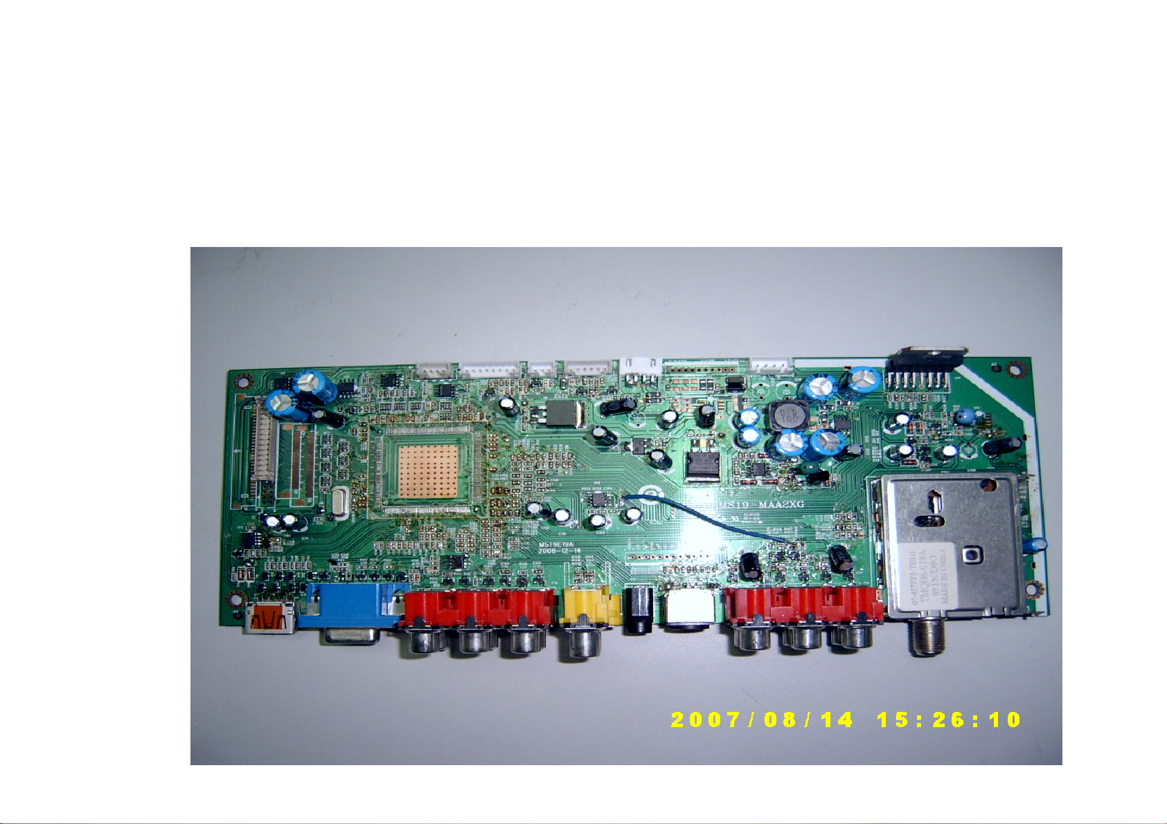
I. picture for Chassis
(1) Chassis
Page 53

(2) Output and input connectors
For
software
upgrade
LVDS
On/off
control
To
inventor
board
To key
board
Power
supply
Earphone
output
Audio
output
HDMI
Input
VGA
input
AV OUT
Y1,Pb1,Pr1
Audio
input of
HDTV
and PC
S video
input
AV1 input
AV3 input
Page 54

(3) Function introduction of ICs
DC-DC
converter
EEPROM
SAVE
CHANNEL
INFORMATI
ON
HPDC
DATA
EEPROM
Save main
software
Earphone
amplifier
Dual-
MOSFET
Power
IC
Audio
power
amplifier
For save HDMI’s
EDID
For save
VGA’s
EDID
Tuner
Page 55
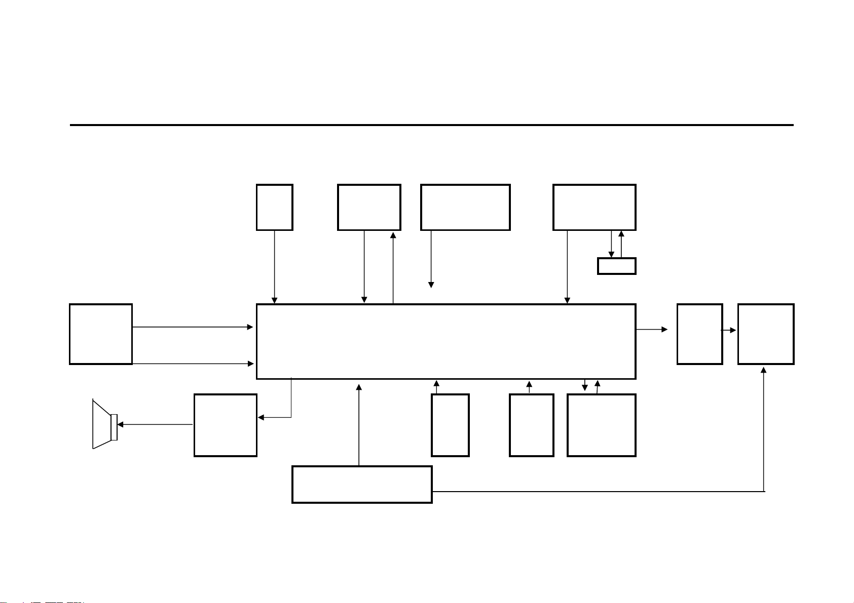
Block Diagram of MS19 By Holt July5,2007
Z1
TUNER
speakerX2
TV CVBS Pin 49/50
SIFP/SIFM Pin54/55
Audio
Pin1/2
Pin14/15
Amplifier
U19
TDA7266SA
AV1/2
INPUT
P14
Pin42-51 Pin61-69
Pin74/75 Pin144 Pin148
POWER SUPPLY
08-LON37A-PW1W
Y/Pb/Pr
AV OUT
P16
Pin16/17 22-28
Main IC U8 MST9E19A
Flash
U9
W25X40
KEY
BOARD
HDMI P12VGA U13
U12
Pin1/2/4/5/7/8
/11/12/14/15
U11 HDCP
IIC
SCL/SDA
LVDS
INTERFERE
NCE P10
Panel
Page 56

Page 57

Page 58

5
P1
C8
0.1uFC80.1uF
C14
C14
0.1uF
0.1uF
3
2
1
CON6_2.0
CON6_2.0
4
3
2
1
10
9
8
7
6
5
4
3
2
1
P1
On/off
GND
+5V
P2
P2
GND
GND
+12V
+12V-AMP
CON6_4.0
CON6_4.0
P3
P3
+12V
+12V
+12V
+12V
GND
GND
GND
GND
+5V
+5V
CON6_2.0
CON6_2.0
ON-PBACK
ADJ-PWM2
On/off
+5Vstb
+12V
+12V_AMP
D D
+12V
C C
+5V
+5Vstb
In standby,+5Vstb can provide 200mA current
R1
4.7KR14.7K
On/off
Q1
NC/3904Q1NC/3904
R2NCR2
NC
R3
4.7KR34.7K
1
2 3
TO Inverter Board
R140R14
0
ON-PBACK
ADJ-PWM2
R17NCR17
NC
POWER-ON/OFFPOWER-ON/OFF
Q3
1
NC(3904)Q3NC(3904)
2 3
4
POWER-ON/OFF
+5Vstb
R19
R19
4.7K
4.7K
R91KR9
R10
R10
1K
10K
10K
R120R12
0
Q2
1
3904Q23904
R181KR18
1K
2 3
Q4
1
3904Q43904
2 3
R8NCR8
NC
R15
R15
4.7K
4.7K
R6
0/NCR60/NC
R4
0/NCR40/NC
BL-ON/OFF
BL-ADJUST
C16
C16
2.2uF
2.2uF
C15
C15
0.1uF
0.1uF
+12V_Inverter
L4L4
6
5
4
3
2
1
P4
P4
GND
Select
Adjust
On/off
+12V
+12V
CON6_2.0
CON6_2.0
3
+12V
C2
C2
C1
C1
+
+
470uF/25V
470uF/25V
470uF/25V
470uF/25V
+
+
0.1uC30.1u
C3
C171uC17
1u
R13
R13
91K
91K
C5
3.3nFC53.3nF
C6
2.2nFC62.2nF
R7
1.5K 1%R71.5K 1%
U1
VCC5LGATE/OCSET
6
FB
7
COMP/SD
8
PHASE
C7
22nFC722nF
R5 11k 1%R5 11k 1%
R1139R11
ISL8105U1ISL8105
39
2
GND
UGATE
BOOT
DC 12V-5V
4
3
2
1
C4
0.1uFC40.1uF
R16
R16
4.7K
4.7K
+
+
C9 470uF/16V
C9 470uF/16V
1
s1
2
g1
3
s2
4
g2
+
+
C10 470uF/16V
C10 470uF/16V
D13N03U2D13N03
C111uC11
1u
1
L1
15uHL115uH
U2
8
d1
7
d1
6
d2
5
d2
+5V
C13
C13
C12
C12
0.01u
0.01u
0.1u
0.1u
Panel Power Source
3
1
2
L14 600(4.5X3.2)L14 600(4.5X3.2)
C28
C28
220uF/16V
220uF/16V
2
Q14
Q14
3904
3904
+12V_Inverter
+
C29
+
C29
47uF/16V
47uF/16V
40V
+12V
PWM3
L6 100uHL6 100uH
R21 4.7KR21 4.7K
D5 1N4148D5 1N4148
Q5
2SC1815Q52SC1815
C18
C18
+
+
10uF/50V
10uF/50V
For tuner 33V
Title
Title
Title
<Title>
<Title>
<Title>
Size Document Number Rev
Size Document Number Rev
Size Document Number Rev
A3
A3
A3
Date: Sheet of
Date: Sheet of
Date: Sheet of
SYSTEM POWER
SYSTEM POWER
SYSTEM POWER
1
110Monday, June 04, 2007
110Monday, June 04, 2007
110Monday, June 04, 2007
2.0
2.0
2.0
M1-D
M2-D
VCC-Panel
8
7
6
5
for big panel use.
+12V +12V_AMP
L8 NCL8 NC
L9 NCL9 NC
POWER-ON/OFF
POWER-ON/OFF
+
+
C25
C25
47uF/16V
47uF/16V
R260R26
0
R27NCR27
NC
C26
C26
0.1uF
0.1uF
R25
R25
10K
10K
Q7
1
3904Q73904
2 3
+12V
R142
R142
10K
10K
D1
1N4148D11N4148
U4
IRF7314U4IRF7314
1
S1
2
G1
3
S2
4
G2
8
D1
7
D1
6
D2
5
D2
tcl-modified
1
LG-PHILIPS LC320W 12V
B B
PANEL-ON/OFF
A A
CMO 5V
Some small panel 3.3V
+3.3V
+12V
+5V
L7
L7
600(4.5X3.2)
600(4.5X3.2)
L10
L10
NC/600(4.5X3.2)
NC/600(4.5X3.2)
L11
L11
NC/600(4.5X3.2)
NC/600(4.5X3.2)
L12
L12
600(4.5X3.2)
600(4.5X3.2)
L13
L13
600(4.5X3.2)
600(4.5X3.2)
PANEL-ON/OFF
R23
R23
4.7K
4.7K
C19
C19
+
+
470uF/16V
470uF/16V
C27
C27
0.1uF
0.1uF
C20
C20
0.1uF
0.1uF
R22
R22
10K
10K
1
2 3
R24NCR24
NC
Q6
3904Q63904
C21
C21
0.1uF
0.1uF
U3A
U3A
SP8J3
SP8J3
M1-S1M1-D
2
M1-G
U3B
U3B
SP8J3
SP8J3
3
M2-S
M2-G4M2-D
32
Q13
Q13
3906
3906
C17A
C17A
+
+
470uF/16V
470uF/16V
+12V_AMP+12V
C24
C24
0.1uF
0.1uF
R143
R143
10K
10K
L15 600(4.5X3.2)L15 600(4.5X3.2)
+
+
In standby,save power,only for small panel use.
5
4
3
Page 59

5
Vcc3.3for MST9E19A analog
ADJ
ADJ
4
OUT
OUT
4
U5
U5
AMS1117-3.3
AMS1117-3.3
IN
IN
3
2
1
Vcc1.8 for MST9E19A
1.25*(1+Rdown/Rup)=3.3V---Rup=510, Rdown=820
3
2
D D
+5Vst
L16FBL16
FB
+3.3AVDD for
AVDD_HDMI
+3.3VA AVDD_HDMI
L41FBL41
C C
FB
C38
C38
2.2uF
2.2uF
1
C30
C30
0.1uF
0.1uF
pin6,pin12
C39
C39
0.1uF
0.1uF
C31
C31
+
+
47uF/16V
47uF/16V
+3.3AVDD for
AVDD_AU
C40
C40
0.1uF
0.1uF
+3.3VA
+3.3AVDD for
AVDDA
+3.3VA AVDDA
L20FBL20
FB
pin36
+3.3AVDD
for AVDD_SIF
C44
C44
2.2uF
2.2uF
3.3V for
AVDDPLL2
B B
+3.3VA AVDD_MemPLL
L22FBL22
FB
C50
C50
2.2uF
2.2uF
C45
C45
0.1uF
0.1uF
C51
C51
0.1uF
0.1uF
+3.3V for
VDD_MPLL
+3.3VA
+3.3VA
C32
C32
0.1uF
0.1uF
L19FBL19
FB
+3.3VA AVDD_SIF
L23FBL23
FB
C33
C33
+
+
47uF/16V
47uF/16V
+5Vstb
AVDD_AU
C41
C41
2.2uF
2.2uF
L21FBL21
FB
VDD_MPLL
1 2
C54
C54
2.2uF
2.2uF
+5V
C46
C46
2.2uF
2.2uF
C42
C42
0.1uF
0.1uF
C55
C55
0.1uF
0.1uF
C47
C47
0.1uF
0.1uF
C56
C56
0.1uF
0.1uF
D8
D8
FM120
FM120
D6
D6
FM120
FM120
D7
D7
FM120/1A
FM120/1A
+5Vst
L18 FBL18 FB
L17 FBL17 FB
C34
U6
U6
4
AP1084-adj
AP1084-adj
+3.3V Regulator
+3.3V Regulator
TO-263
TO-263
IN
IN
OUT
OUT
ADJ
ADJ
R290R29
0
C34
0.1uF
0.1uF
3
2
1
R28NCR28
NC
C36
C36
0.1uF
0.1uF
+3.3V
+
+
+
+
C35
C35
47uF/16V
47uF/16V
C37
C37
47uF/16V
47uF/16V
1.25*(1+Rdown/Rup)=1.8V---Rup=1.2K, Rdown=510
Vcc1.8 for
C48
C48
47uF/16V
47uF/16V
C49
C49
0.1uF
0.1uF
0.1uF
0.1uF
+3.3V
1.8V
MST9E19A
U7
U7
4
AP1084-adj
AP1084-adj
+1.8V Regulator
+1.8V Regulator
TO-263
TO-263
IN
IN
OUT
OUT
ADJ
ADJ
3
2
1
R310R31
C53 47uF/16V
C53 47uF/16V
0
R30NCR30
NC
+
+
VDDC
C52
C52
+
+
Vcc3.3for MST9E19A
VDDC for MST9E19A Core
Digital
+3.3V VDDP VDDC
L24FBL24
A A
FB
+
+
5
C57
C57
47uF/16V
47uF/16V
C58
C58
0.1uF
0.1uF
C59
C59
0.1uF
0.1uF
C60
C60
0.1uF
0.1uF
C61
C61
0.1uF
0.1uF
C62
C62
0.1uF
0.1uF
4
C63
C63
0.1uF
0.1uF
C64
C64
0.1uF
0.1uF
C65
C65
0.1uF
0.1uF
C66
C66
0.1uF
0.1uF
C67
C67
0.1uF
0.1uF
C68
C68
0.1uF
0.1uF
3
C69
C69
0.1uF
0.1uF
C70
C70
0.1uF
0.1uF
C71
C71
0.1uF
0.1uF
C72
C72
0.1uF
0.1uF
Title
Title
Title
C73
C73
0.1uF
0.1uF
<Title>
<Title>
<Title>
Size Document Number Rev
Size Document Number Rev
Size Document Number Rev
A4
A4
A4
Date: Sheet
Date: Sheet
Date: Sheet
2
LDO DC-DC ?
LDO DC-DC ?
LDO DC-DC ?
210Monday, June 04, 2007
210Monday, June 04, 2007
210Monday, June 04, 2007
1
of
of
of
Page 60
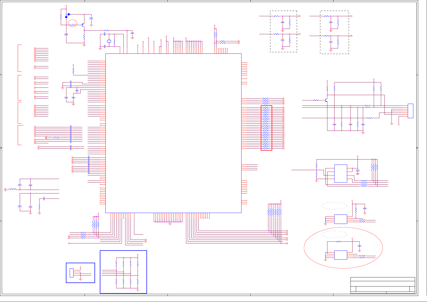
5
D D
R_TX2+
R_TX2+
R_TX2-
R_TX2-
G_TX1+
G_TX1+
G_TX1-
G_TX1-
B_TX0+
B_TX0+
B_TX0-
B_TX0TXCLK+
TXCLK-
HDMI_SDA
HDMI_SCL
HS_RGB
VS_RGB
SC_SOG
AV1-Cin
AV1-Yin
AV1-YinAV1-Vin+
AV2-Vin+
AV3-Vin+
TV1-Vin+
TV1-Vin-
CVBSOut
TXCLK+
TXCLK-
HDMI_SDA
HDMI_SCL
HS_RGB
VS_RGB
BIN+
BIN+
BIN-
BIN-
SOG
SOG
GIN+
GIN+
GIN-
GIN-
RIN+
RIN+
RIN-
RIN-
SC_SOG
SCR+
SCR+
SCR-
SCR-
SCG+
SCG+
SCG-
SCG-
SCB+
SCB+
SCB-
SCB-
AV1-Cin
AV1-Yin
AV1-YinAV1-Vin+
AV2-Vin+
AV3-Vin+
TV1-Vin+
TV1-VinCVBSOut
TV-SIFP SIFP
TV-SIFP
TV-SIFM SIFM
TV-SIFM
C114
C114
0.1uF
0.1uF
C115
C115
2.2uF
2.2uF
C116
C116
R670R67
0.1uF
0.1uF
0
DVI
INPUT
VGA
INPUT
C C
SCART
INPUT
VIDEO
INPUT
C113
B B
C113
10uF/16V
10uF/16V
L250L25
0
C118
C118
10uF/16V
10uF/16V
R32
R32
10K
10K
R64 47R64 47
AUVRADP
AUVRADN
AUVREF
AUCOM
+3.3V
3
2
D40
D40
BAV99
BAV99
1
R391KR39
1K
C80
C80
10uF/16V
10uF/16V
AVDD_HDMI
R53
R53
390R1%
390R1%
C87
C87
0.1uF
0.1uF
C85
C85
0.1uF
0.1uF
C86
C86
0.1uF
0.1uF
C89
C92 10nFC92 10nF
C93 10nFC93 10nF
C94 10nFC94 10nF
C96 10nFC96 10nF
C97 10nFC97 10nF
C98 10nFC98 10nF
C99 10nFC99 10nF
C100 10nFC100 10nF
C101 10nFC101 10nF
C102 0.1uFC102 0.1uF
C103 0.1uFC103 0.1uF
PC-Lin
PC-Rin
AV1-Lin
AV1-Rin
AV2-Lin
AV2-Rin
AV3-Lin
AV3-Rin
TXD
RXD
AFT
SDA
SCL
TXD
RXD
AFT
C89
0.1uF
0.1uF
SV_C0
SV_Y0
VCOM2
CVBS3
CVBS2
CVBS1
VCOM1
TUNER_CVBS
VCOM0
PC-Lin
PC-Rin
AV1-Lin
AV1-Rin
AV2-Lin
AV2-Rin
AV3-Lin
AV3-Rin
R71 10R71 10
R72 10R72 10
R73 10R73 10
R74 10R74 10
C88
C88
0.1uF
0.1uF
C74
C74
47uF/16V
47uF/16V
Q8
1
3906Q83906
3 2
R42
R42
10K
10K
TUNER_CVBS
C104 2.2uFC104 2.2uF
C105 2.2uFC105 2.2uF
C106 2.2uFC106 2.2uF
C107 2.2uFC107 2.2uF
C108 2.2uFC108 2.2uF
C109 2.2uFC109 2.2uF
C110 2.2uFC110 2.2uF
C111 2.2uFC111 2.2uF
SYS_RST
TXCLKTXCLK+
B_TX0B_TX0+
G_TX1G_TX1+
R_TX2R_TX2+
HDMI_SDA
HDMI_SCL
HS_RGB
VS_RGB
BIN+
BINSOG
GIN+
GINRIN+
RIN-
SCBSCB+
SCGSCG+
SC_SOG
SCRSCR+
SV_C0
SV_Y0
VCOM2
CVBS3
CVBS2
CVBS1
VCOM1
VCOM0
CVBSOut
SIFP
SIFM
AUVRADN
AUVRADP
AUVREF
AUCOM
PH-Lout
PH-Rout
AMP-Lout
AMP-Rout
+3.3V
R40
R40
100
100
C78
C78
22pF
22pF
Y1
C84
C84
1 2
14.318MHZY114.318MHZ
22pF
22pF
1
RXCKN
2
RXCKP
4
RX0N
5
RX0P
7
RX1N
8
RX1P
10
RX2N
11
RX2P
13
REXT
14
DDCD_DA
15
DDCD_CK
16
HSYNC1
17
VSYNC1
18
RMID
19
VCLAMP
20
REFP
21
REFM
22
BIN1P
23
BIN1M
24
SOGIN1
25
GIN1P
26
GIN1M
27
RIN1P
28
RIN1M
29
BIN0M
30
BIN0P
31
GIN0M
32
GIN0P
33
SOGIN0
34
RIN0M
35
RIN0P
38
HSYNC0
39
VSYNC0
40
C1
41
Y1
42
C0
43
Y0
44
VCOM2
45
CVBS3
46
CVBS2
47
CVBS1
48
VCOM1
49
CVBS0
50
VCOM0
51
CVBSOUT
54
SIF1P
55
SIF1M
57
AUVRADN
58
AUVRADP
59
AUVREF
61
AUL0
62
AUR0
63
AUL1
64
AUR1
65
AUCOM
66
AUL2
67
AUR2
68
AUL3
69
AUR3
70
AUOUTL3
71
AUOUTR3
72
AUOUTL2
73
AUOUTR2
74
AUOUTL
75
AUOUTR
76
AUOUTS
78
GPIOF2
79
GPIOF3
80
GPIOF4
81
GPIOF5
82
GPIOF6
83
GPIOF7
84
GPIOF8
85
GPIOF9
86
GPIOF10
87
GPIOF11
131
7531
7531
RP10
RP10
RP4.7KX4
RP4.7KX4
8642
8642
I2C-SDA
I2C-SCL
DDC-TXD
DDC-RDX
KEY0
KEY1
Mode Selection
A A
5
Debug port
+5Vstb
P6
1
2
RXD
3
4
CN-SCN-5YP6CN-SCN-5Y
PWM3
ADJ-PWM2
WP_FSH
PWM0TXD
DDCR_DA
DDCR_CK
132
133
R481MR48
1M
DDCA_DA
DDCA_CK
SAR0
134
125
R781KR78
1K
R82NCR82
NC
207
126
XIN
SAR1
127
206
XOUT
SAR2
SAR3
128
129
R79NCR79
NC
R831KR831KR841KR84
4
205
HWRESET
PWM0
PWM1
130
4
155
PWM2
156
C79
C79
100pF
100pF
PWM3
136
PWM3
ADJ-PWM2
WP_FSH
PWM0
R80NCR80
NC
1K
AVDDA
IRIN
IR_SYNC
+3.3V
AVDD_SIF
36
AVDD_ADC
R811KR81
1K
R85NCR85
NC
AVDD_AU
53
AVDD_SIF
AVDD_MemPLL
60
AVDD_AU
PWM3
ADJ-PWM2
VDD_MPLL
AVDD_HDMI
105
12
AVDD_DVI6AVDD_DVI
AVDD_MEMPLL
MST9E19A
MST9E19A
GND3GND9GND37GND52GND56GND89GND99GND
GND
209
157
208
AVDD_MPLL
AVDD_MPLL
U8
U8
GND
101
104
VDDC
GND
106
107
VDDC77VDDC98VDDC
GND
GND
120
141
152
3
Location Near IC Pin.
R33
R33
AMP-Rout
100
100
+3.3V
R45
R45
AMP-Lout
100
RP1
RP1
33
33
7531
7531
7531
7531
7531
7531
7531
7531
7531
7531
7531
7531
7531
7531
RP2 0/33
RP2 0/33
RP5 0/33
RP5 0/33
RP4 0/33
RP4 0/33
RP3 0/33
RP3 0/33
RP6 0/33
RP6 0/33
RP7 0/33
RP7 0/33
RP12
RP12
RP4.7KX4
RP4.7KX4
8642
8642
8642
8642
8642
8642
8642
8642
8642
8642
8642
8642
8642
8642
7531
7531
8642
8642
100
LVSYNC
LHSYNC
LDE
LCK
RXO0-/R7
RXO0+/R6
RXO1-/R5
RXO1+/R4
RXO2-/R3
RXO2+/R2
RXOC-/R1
RXOC+/R0
RXO3-/G7
RXO3+/G6
RXO4-/G5
RXO4+/G4
RXE0-/G3
RXE0+/G2
RXE1-/G1
RXE1+/G0
RXE2-/B7
RXE2+/B6
RXEC-/B5
RXEC+/B4
RXE3-/B3
RXE3+/B2
RXE4-/B1
RXE4+/B0
7531
7531
8642
8642
R44
R44
R43
R43
10K
10K
10K
140
148
VDDP
DIGO5
151
149
VDDP
DIGO6
159
150
VDDP
DIGO7
172
153
VDDP
DIGO8
186
154
VDDP
DIGO9
10K
R49
R49
SCL_EXT
100
100
R52
R52
100
100
113
112
111
110
109
108
AD5
AD4
AD3
AD2
AD1
AD0
WRZ
RDZ
ALE
INT
116
117
118
135
POWER-ON/OFF
ON-PBACK
HPDCTRL
LED1
PANEL-ON/OFF
AMP-MUTE
WP
3
SDA_EXT
115
114
AD7
AD6
GPIOE0/LVSYNC
GPIOE1/LHSYNC
GPIOE2/LDE
GPIOE3/LCK
PWM_SENSE
IVSYNC
IHSYNC
LB0M/R7
LB0P/R6
LB1M/R5
LB1P/R4
LB2M/R3
LB2P/R2
LBCKM/R1
LBCKP/R0
LB3M/G7
LB3P/G6
LB4M/G5
LB4P/G4
LA0M/G3
LA0P/G2
LA1M/G1
LA1P/G0
LA2M/B7
LA2P/B6
LACKM/B5
LACKP/B4
LA3M/B3
LA3P/B2
LA4M/B1
LA4P/B0
GPIOF19
GPIOF18
GPIOF17
GPIOF16
GPIOF15
GPIOF14
GPIOF13
GPIOF12
PWM_DRV
PWM_FB
ICLK
SDO
CSZ
SCK
DI7
DI6
DI5
DI4
DI3
DI2
DI1
DI0
SDI
SCL_EXT
SDA_EXT
202
201
200
199
198
197
196
195
192
194
193
191
190
189
188
185
184
183
182
181
180
179
178
177
176
175
174
171
170
169
168
167
166
165
164
163
162
161
160
124
123
122
121
97
96
95
94
93
92
91
90
139
138
137
Audio Output(to Amp)
for TTL output
TTL-LVSYNC
TTL-LHSYNC
TTL-LDE
TTL-LCK
TTL-RED7
TTL-RED6
TTL-RED5
TTL-RED4
TTL-RED3
TTL-RED2
TTL-RED1
TTL-RED0
TTL-GREEN7
TTL-GREEN6
TTL-GREEN5
TTL-GREEN4
TTL-GREEN3
TTL-GREEN2
TTL-GREEN1
TTL-GREEN0
TTL-BLUE7
TTL-BLUE6
TTL-BLUE5
TTL-BLUE4
TTL-BLUE3
TTL-BLUE2
TTL-BLUE1
TTL-BLUE0
SPI_DO
SPI_CZ
SPI_DI
SPI_CK
VDDP
100
102
103
119
142
158
203
VDDP88VDDP
VDDP
VDDP
VDDP
VDDC
VDDC
VDDC
GND
GND
GND
GND
DIGO0
DIGO1
DIGO2
DIGO3
173
DIGO4
187
204
143
144
145
146
147
+3.3V
C76
C76
10nF
10nF
C82
C82
10nF
10nF
LVSYNC
LHSYNC
LDE
LCK
RXO0-/R7
RXO0+/R6
RXO1-/R5
RXO1+/R4
RXO2-/R3
RXO2+/R2
RXOC-/R1
RXOC+/R0
RXO3-/G7
RXO3+/G6
RXO4-/G5
RXO4+/G4
RXE0-/G3
RXE0+/G2
RXE1-/G1
RXE1+/G0
RXE2-/B7
RXE2+/B6
RXEC-/B5
RXEC+/B4
RXE3-/B3
RXE3+/B2
RXE4-/B1
RXE4+/B0
RP13
RP13
RP4.7KX4
RP4.7KX4
2
Location Near IC Pin.
R34
PH-Lout
R34
100
100
R47
R47
100
100
AMP-R
AMP-R PH-R1out
R38
R38
22K
22K
AMP-L
AMP-L
R50
R50
22K
22K
AV Output(Audio)
+5Vstb
R54
R54
4.7K
4.7K
R58
R58
4.7K
4.7K
WP_FSH
POWER-ON/OFF
ON-PBACK
HPDCTRL
PANEL-ON/OFF
AMP-MUTE
GPIO-0
2
LED1
KEY0
KEY1
IR_SYNC
Q9
1
3904Q93904
2 3
Mstar PULL UP
SST PULL DOWN
R65NCR65
NC
R66
R66
1.8K
1.8K
I2C address
at A0.
HDCP I2C address
at A4.
C77
C77
1nF
1nF
C83
C83
1nF
1nF
U9
W25X40U9 W25X40
1
CE#
2
SO
3
WP#
VSS4SI
U10
U10
24C32
24C32
1
A0
2
A1
3
A2
GND4SDA
U11
U11
24C04
24C04
1
A0
2
A1
3
A2
GND4SDA
1
PH-R1outPH-Rout
R36
R36
22K
22K
PH-L1out
PH-L1out
R51
R51
22K
22K
+3.3V
R56
RP9
RP9
RP33X4
RP33X4
7531
7531
C119
C119
0.1uF
0.1uF
R591KR59
1K
R601KR60
1K
C95
C95
100pF
100pF
R69
R69
100
100
R70
R70
100
100
R76
R76
100
100
R77
R77
100
100
R6110R61
10
C117
C117
0.1uF
0.1uF
8642
8642
SCL
SDA
SCL
SDA
R56
8.2K
8.2K
7531
7531
8642
8642
1
R55
R55
4.7K
4.7K
C90
C90
100pF
100pF
R75
R75
10K
10K
HOLD#
R62NCR62
NC
VDD
SCK
VCC
WP
SCL
VCC
WP
SCL
R63NCR63
C91
C91
NC
100pF
100pF
+3.3V
8
C112
C112
0.1uF
0.1uF
7
6
5
+5Vstb
R68
R68
10K
10K
8
WP
7
6
5
+5Vstb
8
WP
7
6
5
Title
Title
Title
<Title>
<Title>
<Title>
Size Document Number Rev
Size Document Number Rev
Size Document Number Rev
A2
A2
A2
Date: Sheet
Date: Sheet
Date: Sheet
R57
R57
8.2K
8.2K
KEY0-in
KEY1-in
RP8
RP8
RP4.7KX4
RP4.7KX4
SPI_CK
SPI_DI
SPI_CZ
SPI_DO
MST9E19A ?
MST9E19A ?
MST9E19A ?
P5
1
2
3
4
IR-IN
5
LED
6
7
CON6_2.0P5CON6_2.0
+5Vstb
of
310Monday, June 04, 2007
of
310Monday, June 04, 2007
of
310Monday, June 04, 2007
Page 61
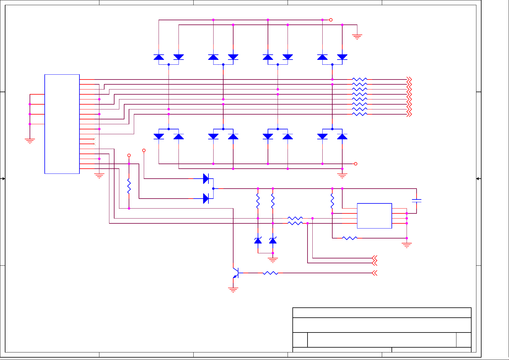
5
4
3
2
1
+5V
2
2
3
3
D17
D17
BAT54C
BAT54C
3
1
1
D10
D10
BAV99
BAV99
D14
D14
BAV99
BAV99
R95
R95
4.7K
4.7K
D D
2
P12
P12
HDMI_J
HDMI_J
HDMI/5V
HDMI-RX2+
HDMI-RX2HDMI-RX1+
HDMI-RX1HDMI-RX0+
HDMI-RX0HDMI-RXC+
HDMI-RXC-
+5V
2
CLK+
CLK-
CEC
NC
SCL
SDA
1
2
3
4
5
6
7
8
9
10
11
12
13
14
15
16
17
18
19
DATA2+
DATA2 SHIELD
20
GND1
21
GND2
22
GND3
23
GND4
C C
DATA2-
DATA1+
DATA1 SHIELD
DAT1A-
DATA0+
DATA0 SHIELD
DATA0-
CLK SHIELD
DDC/CEC GND
+5V POWER
HOT PLUG
1
D9
D9
BAV99
BAV99
3
3
D13
D13
BAV99
BAV99
1
2
2
1
R941KR94
1K
2
HDMI-HPD
HDMI-DDC-SCL
B B
HDMI-DDC-SDA
D18
D18
5.6V
5.6V
1 2
R1011KR101
Q10
Q10
3904
3904
1K
1
1
D11
D11
BAV99
BAV99
2
3
3
D15
D15
BAV99
BAV99
1
2
1
3
R86 10R86 10
R87 10R87 10
R88 10R88 10
R89 10R89 10
R90 10R90 10
R91 10R91 10
R92 10R92 10
R93 10R93 10
3
1
D12
D12
BAV99
BAV99
D16
D16
BAV99
BAV99
R_TX2+
R_TX2G_TX1+
G_TX1B_TX0+
B_TX0TXCLK+
TXCLK-
R_TX2+
R_TX2G_TX1+
G_TX1B_TX0+
B_TX0TXCLK+
TXCLK-
+5V
U12
R1000R100
0
8
7
6
5
U12
24C02
24C02
VCC
WP
SCL
SDA
1
NC
2
NC
3
NC
4
GND
HDMI_SCL
HDMI_SDA
HPDCTRL
C120
C120
0.1uF
0.1uF
R97NCR97
R96
R96
4.7K
4.7K
R98
R98
100
100
R99
R99
100
100
D19
D19
5.6V
5.6V
1 2
NC
HDMI_SCL
HDMI_SDA
HPDCTRL
2 3
A A
Title
Title
Title
Size Document Number Rev
Size Document Number Rev
Size Document Number Rev
Date: Sheet of
Date: Sheet of
5
4
3
Date: Sheet
<Title>
<Title>
<Title>
A
A
A
2
HDMI ?
HDMI ?
HDMI ?
of
410Monday, June 04, 2007
410Monday, June 04, 2007
410Monday, June 04, 2007
1
Page 62

5
4
3
2
1
VGA/5V
P13
P13
VGA
VGA
15
14
D D
13
12
11
5
10
4
9
3
8
2
7
1
6
16
17
VGA-B+
VGA-G+
VGA-R+
R144
R144
100
100
PROTECT
D20
D20
STZ6.2N
STZ6.2N
3
2 1
2 1
D21
D21
STZ6.2N
STZ6.2N
3
2 1
D22
D22
STZ6.2N
STZ6.2N
3
R10775R107
75
R10875R108
75
R10975R109
75
R10310R103
10
R10410R104
10
R10510R105
10
R106
R106
330
330
R11047R110
47
R11147R111
47
R11347R113
47
C121
C121
47nF
47nF
C122
C122
47nF
47nF
C123
C123
47nF
47nF
C124
C124
1nF
1nF
C125
C125
47nF
47nF
C126
C126
47nF
47nF
C127
C127
47nF
47nF
BIN+
GIN+
RIN+
SOG
BINGINRIN-
BIN+
GIN+
RIN+
SOG
BINGINRIN-
R172 10KR172 10K
R173 10R173 10
+5VSTB
R174
R174
R171 1KR171 1K
R1141KR114
1K
R1151KR115
1K
+5VSTB
10k
10k
HS_RGB
VS_RGB
S
D
S
D
Q18Q18
Q19Q19
1
C19
C19
0.1uF
0.1uF
2 3
HS_RGB
VS_RGB
Q25
Q25
3904
3904
TXD
RXD
TXD
RXD
+3.3V
R170
R170
4.7K
4.7K
D23
D23
BAT54C
BAT54C
VGA-HS
VGA-VS
VGA-SDA
VGA-SCL
D25
D25
STZ6.2N
STZ6.2N
2 1
R118
R118
4.7K
4.7K
R119
R119
4.7K
4.7K
R116
R116
10K
10K
C128NCC128
NC
R117
R117
4.7K
4.7K
C129NCC129
NC
D24
D24
STZ6.2N
STZ6.2N
2 1
3
C C
+5v
1
2
3
3
R122
R122
4.7K
U13
U13
24C02
C130
C130
0.1uF
0.1uF
B B
24C02
1
NC
2
NC
3
NC
GND4SDA
VCC
VCLK
SCL
8
7
6
5
4.7K
R12010R120
10
R12110R121
10
VGA-SDA
PROTECT
R123NCR123
NC
D2 STZ6.2ND2 STZ6.2N
3
VGA-SCL
GPIO-0
175 10175 10
2 1
Program Control
A A
Title
Title
Title
<Title>
<Title>
<Title>
Size Document Number Rev
Size Document Number Rev
Size Document Number Rev
Custom
Custom
Custom
Date: Sheet
Date: Sheet
5
4
3
Date: Sheet
2
VGA ?
VGA ?
VGA ?
of
510Monday, June 04, 2007
of
510Monday, June 04, 2007
of
510Monday, June 04, 2007
1
Page 63

5
AV INPUT
AV1-V
AV1-L
AV1-R
AV3-V
AV3-L
AV3-R
3
3
3
3
21
3
3
21
21
D26
D26
STZ6.2N
STZ6.2N
R134 10KR134 10K
21
D28
D28
STZ6.2N
STZ6.2N
R138 10KR138 10K
D33
D33
STZ6.2N
STZ6.2N
21
D34
D34
STZ6.2N
STZ6.2N
R154 10KR154 10K
21
D36
D36
STZ6.2N
STZ6.2N
R160 10KR160 10K
D37
D37
STZ6.2N
STZ6.2N
P14
P14
V1
V1
2
1
1
L1
L1
5
4
D D
C C
4
R1
R1
8
7
7
10
10
11
11
3
V2
V2
6
L2
L2
9
R2
R2
AV1
AV1
4
CA1 47uF/16VCA1 47uF/16V
AV3-Vin+
R127 10R127 10
C132
C132
R12975R129
680pF
680pF
75
AV3-Lin
C134
C134
R135
R135
560pF
560pF
12K
12K
AV3-Rin
R145
R145
C138
C138
12K
12K
560pF
560pF
AV1-Vin+
R148 10R148 10
C140
C140
R14975R149
680pF
680pF
75
AV1-Lin
R157
R157
C142
C142
12K
12K
560pF
560pF
AV1-Rin
R161
R161
C146
C146
12K
12K
560pF
560pF
AV3-Vin+
AV3-Lin
AV3-Rin
AV1-Vin+
AV1-Lin
AV1-Rin
5VPI
R124
R124
10K
10K
AV-SOG
R125
R125
10K
10K
P15
P15
3 4
5 7
S-VIDEO-Jack
S-VIDEO-Jack
2PJ-4018-001
2PJ-4018-001
P7
P7
GND
GND
1
L
L
2
R
R
3
AV1X2
AV1X2
21
6
3
2
1
S-Video Input (Y/C)
R12610R126
R12875R128
75
R13675R136
75
PC-Lin
PC-Rin
C131
C131
680pF
680pF
C136
C136
680pF
680pF
PC-Lin
PC-Rin
10
AV1-Yin
AV1-Yin
R13347R133
47
AV1-Yin-
AV1-Yin-
R13710R137
10
AV1-Cin
AV1-Cin
P16
P16
1
4
7
10
11
1
4
7
10
11
AV1
AV1
V1
V1
L1
L1
R1
R1
V2
V2
L2
L2
R2
R2
2
5
8
3
6
9
HDTV In
21
D30
D30
3
STZ6.2N
STZ6.2N
AV Output
Scart2_L
Scart2_R
Y1
Pb1
Pr1
21
R13975R139
75
D31
D31
3
STZ6.2N
STZ6.2N
Video_out2SCART2_VOUT Video_out2
21
D35
D35
3
STZ6.2N
STZ6.2N
21
D39
D39
3
STZ6.2N
STZ6.2N
21
R14075R140
75
C139
C139
0.1uF
0.1uF
Q11
Q11
3906
3906
R15175R151
75
21
3
3
3 2
D38
D38
STZ6.2N
STZ6.2N
R153
R153
220
220
D32
D32
STZ6.2N
STZ6.2N
1
+5V
Q12
Q12
3904
3904
C144 2.2uFC144 2.2uF
C145 2.2uFC145 2.2uF
R14175R141
75
R147
R147
R146
R146
10K
10K
330
330
C218
C218
10uF/16V
10uF/16V
1
2 3
R155
R155
220
220
CVBSOut
CVBSOut
R156
R156
10K
10K
Scart2_Lout
Scart2_Lout
Scart2_Rout
Scart2_Rout
AV1-Y
21
D27
D27
3
STZ6.2N
STZ6.2N
AV1-C
21
D29
D29
3
STZ6.2N
STZ6.2N
R150
R150
10K
10K
PC-L
R152
R152
C141
C141
12K
12K
560pF
560pF
R158
R158
10K
10K
PC-R
C143
C143
R159
R159
560pF
560pF
12K
12K
Y1
R176 470R176 470
Pb1
For SUB AV
R18610R186
C155
C155
680pF
680pF
C162
C162
560pF
560pF
C163
C163
560pF
560pF
10
AV2-Vin+
AV2-Lin
AV2-Lin
R197
R197
12K
12K
AV2-Rin
AV2-Rin
R201
R201
12K
12K
Option
4
AV2-V
R188
R188
NC/75
NC/75
R196
R196
10K
B B
A A
5
AV2-L
AV2-R
10K
R200
R200
10K
10K
R183 10R183 10
Pr1
R184 10R184 10
Y1
R185 10R185 10
R189 47R189 47
R191 47R191 47
R195 47R195 47
P11
P11
1
2
3
4
5
6
7
8
9
10
11
12
CON6_2.0
CON6_2.0
1
2
3
4
5
6
7
8
9
10
11
12
C151 1nFC151 1nF
C152 47nFC152 47nF
C153 47nFC153 47nF
C154 47nFC154 47nF
C156 47nFC156 47nF
C158 47nFC158 47nF
C159 47nFC159 47nF
SC_SOG
SCB+
SCR+
SCG+
SCRSCGSCB-
AMP-Rout+
AMP-Lout+
AMP-Lin
AMP-Rin
AV2-V
AV2-L
AV2-R
SC_SOG
SCB+
SCR+
SCG+
SCRSCGSCB-
AMP-PRout+
AMP-PLout+
AMP-Lin
AMP-Rin
6VBuf2
R225
R225
C183
C183
47K
47K
47uF/16V
47uF/16V
R226
R226
10K
10K
C188
C188
PH-R1out
2.2uF
PH-R1out
2.2uF
AV Output Audio Amp
R230
R230
10K
C191
C191
PH-L1out
2.2uF
PH-L1out
3
2.2uF
10K
+5V
L42 FBL42 FB
R224
R224
47K
47K
OP_VCC2
C184
C184
C185
C185
0.1uF
0.1uF
47uF/16V
47uF/16V
84
5
+
+
6
-
-
R229
R229
33K
33K
C189
C189
100pF
100pF
3
+
+
2
-
-
R232
R232
33K
33K
C193
C193
100pF
100pF
2
84
7
U16B
U16B
TDA1308
TDA1308
OP_VCC2
1
U16A
U16A
TDA1308
TDA1308
Scart2_Rout
Scart2_Lout
Scart2_Rout
Scart2_Lout
Title
Title
Title
<Title>
<Title>
<Title>
Size Document Number Rev
Size Document Number Rev
Size Document Number Rev
A2
A2
A2
Date: Sheet
Date: Sheet
Date: Sheet
INPUT ?
INPUT ?
INPUT ?
1
of
610Monday, June 04, 2007
of
610Monday, June 04, 2007
of
610Monday, June 04, 2007
Page 64

5
Z1
Z1
TUNER_IF
TUNER_IF
GND
GND
GND
GND
21
20
19
18
4
AGND
3
2
1
17
C167
C167
100nF
100nF
AGND
C166
C166
10nF
10nF
R221
R221
22K
22K
R22010R220
10
R202
R202
51K
51K
D47
D47
C33V1
C33V1
R205
R205
NC
33V
C23NCC23
C174NCC174
100K
100K
L34
L34
22uH
22uH
R203
R203
100K
100K
AFT
Close to MST IC
40V
R2041KR204
1K
R207NCR207
NC
R20610R206
10
R21047R210
47
TV1-Vin+
TV1-Vin-
TV1-Vin+
TV1-Vin-
R222
R222
22K
22K
L290L29
0
L300L30
0
L280 L280
NC
C175
C175
100PF
100PF
Tuner Power
POWER-ON/OFF
C181
C181
0.1uF
0.1uF
C182
C182
0.1uF
0.1uF
POWER-ON/OFF
TV-SIFP
TV-SIFM
+5V
+
+
C168
C168
47uF/16V
47uF/16V
R211
R211
4.7K
4.7K
C169
C169
0.1uF
0.1uF
R208
R208
1
10K
10K
Q17
Q17
3904
3904
2 3
1
2
3
4
L32FBL32
FB
U15
U15
IRF7314
IRF7314
S1
G1
S2
G2
D1
D1
D2
D2
NC
5VA
8
7
6
5
C173
C173
0.1uF
0.1uF
NC2
NC1
D D
C164
C164
+
+
4.7uF/50V
C171
C171
AGND
4.7uF/50V
+
+
220uF/16V
220uF/16V
+5V
L27
L27
22uH
22uH
C200
C200
2200PF
2200PF
R209
R209
120
SCL_EXT
C C
SDA_EXT
B B
120
R212
R212
120
120
NC33NC44NC55AUDIO6SIF7GND8SCL9SDA10AGC11MB12NC13TU14GND15AFT16VIDEO
2
1
C165
C165
10nF
10nF
C172
C172
0.1uF
0.1uF
C177
C177
C176
C176
150pF
150pF
100pF
100pF
CVBS Output: Vp-p=1V
SIF
A A
Title
Title
Title
<Title>
<Title>
<Title>
Size Document Number Rev
Size Document Number Rev
Size Document Number Rev
B
B
B
Date: Sheet
Date: Sheet
Date: Sheet
5
4
3
2
TUNER ?
TUNER ?
TUNER ?
of
710Monday, June 04, 2007
of
710Monday, June 04, 2007
of
710Monday, June 04, 2007
1
Page 65

5
AMP-Lin
AMP-Rin
D D
P17
P17
PHONE_JACK_STEREO_SW
PHONE_JACK_STEREO_SW
C195
C195
1nF
1nF
C194
C194
1nF
1nF
AMP-PLoutAMP-PRout-
1
2
3
AMP-PROUT+ AMP-PLOUT+
C C
+
C196
+
C196
100uF/16V
100uF/16V
R251
R251
330
330
5
4
6
9
8
7
EARPHONE-RA
C198
C198
1000PF
1000PF
AMP-LINAMP-RIN
P9
P9
1
2
3
4
5
CON4_2.54
CON4_2.54
+
C197
+
C197
100uF/16V
100uF/16V
R249
R249
330
330
C199
C199
1000PF
1000PF
4
1
2
3
4
5
EARPHONE-LA
3
AMP-L
AMP-L
AMP-R
AMP-R
C204
C204
5Vstb+12V
+12V_AMP
L33FBL33
FB
L31FBL31
12V-2
FB
R1620R162
0
R163NCR163
NC
D3
1N4148D31N4148
R164
R164
10K
10K
C217
C217
220uF/16V
220uF/16V
32
Q15
Q15
1
3906
3906
C213
C213
+
+
470uF/16V
470uF/16V
R165
R165
10K
10K
1
AMP-MUTE=1,MUTE;AMP-MUTE=0,ON;
Q24NCQ24
NC
R254
R254
10K
10K
AMP-MUTE
Q23
Q23
1
AMP-MUTE2
5Vstb
R253NCR253
NC
R2560R256
0
R2570R257
POWER-ON/OFF1,2
POWER-ON/OFF
0
3
1
2
1nF
1nF
R244
R244
3
2
3
2
Q16
Q16
3904
3904
3904
3904
R243
R243
2
C203
C203
C205
C205
C206
C206
1nF
1nF
+
+
10K
10K
10K
10K R166
R166
R167
R167
R252
R252
10K
10K
R255
R255
2.2uF
2.2uF
2.2uF
2.2uF
3.3K
3.3K
3.3K
3.3K
100
100
C209
C209
0.1uF
0.1uF
1
12
4
20
9
6
7
19
3
17
13
22
8
TDA7266SA
TDA7266SA
TDA7266SA+TDA7266NEW
TDA7266SA+TDA7266NEW
R169NCR169
C212
C212
+
+
NC
NC
3
3904
3904
Q22
Q22
2
U19
U19
2IN+
1IN+
20
SGND
AMUTE
Standby
19
VCC1
17
VCC2
22
PWGND
NC
2OUT+
NC1
NC3
2OUT-
1OUT+
NC2
1OUT-
1
15
23
23
5
18
18
11
21
21
14
1
16
16
10
2
R168NCR168
NC
AMP-PLout+
AMP-PLoutAMP-PRout+
AMP-PRout-
H8
3
GND
2
GND
1
GND
POWERH8POWER
B B
H3
H2
H1
H1
NC/HOLE-V8
NC/HOLE-V8
1
5
4
3
2
A A
5
13
9
8
7
6
10101111121213
H2
NC/HOLE-V8
NC/HOLE-V8
5
4
3
2
13
4
1
9
8
7
6
10101111121213
H3
NC/HOLE-V8
NC/HOLE-V8
5
4
3
2
13
1
9
8
7
6
10101111121213
3
H4
H4
NC/HOLE-V8
NC/HOLE-V8
5
4
3
2
13
1
9
8
7
6
10101111121213
Title
Title
Title
<Title>
<Title>
<Title>
Size Document Number Rev
Size Document Number Rev
Size Document Number Rev
A3
A3
A3
Date: Sheet of
Date: Sheet of
2
Date: Sheet
AMPLIFIER TDA7266 ?
AMPLIFIER TDA7266 ?
AMPLIFIER TDA7266 ?
of
810Monday, June 04, 2007
810Monday, June 04, 2007
810Monday, June 04, 2007
1
Page 66
5
D D
4
3
2
FH12-50S-0.5SH(NC)
FH12-50S-0.5SH(NC)
J1
J1
1
51
1
GND
51
2
J3
J3
4647
CON45/FH-12-45S-0.5SH(NC)
LVDS Interface
J2
J2
DF14-30P-1.25H/LVDS
DF14-30P-1.25H/LVDS
C215
C215
0.1uF
0.1uF
RXO0-/R7
RXO0+/R6
RXO1-/R5
RXO1+/R4
RXO2-/R3
RXO2+/R2
RXOC-/R1
RXOC+/R0
RXO3-/G7
RXO3+/G6
RXO4-/G5
RXO4+/G4
RXE0-/G3
RXE0+/G2
RXE1-/G1
RXE1+/G0
RXE2-/B7
RXE2+/B6
RXEC-/B5
RXEC+/B4
RXE3-/B3
RXE3+/B2
RXE4-/B1
RXE4+/B0
+
+
C216
C216
470uF/16V
470uF/16V
1
2
3
4
5
6
7
8
9
10
11
12
13
14
15
16
17
18
19
20
21
22
23
24
25
26
27
28
29
30
31
32
P10
P10
LDE
LDE
LVSYNC
LVSYNC
RXO0-/R7
RXO0-/R7
RXO1-/R5
RXO1-/R5
RXO2-/R3
RXO2-/R3
RXOC-/R1
RXOC-/R1
RXO3-/G7
RXO3-/G7
RXO4-/G5
C C
B B
RXO4-/G5
RXE0-/G3
RXE0-/G3
RXE1-/G1
RXE1-/G1 RXE1+/G0
RXE2-/B7
RXE2-/B7
RXEC-/B5
RXEC-/B5
RXE3-/B3
RXE3-/B3
RXE4-/B1
RXE4-/B1
VCC-Panel
39
37
TTL
TTL
GND35GND
A3+33A3AC-31ACA2+29A2A1+27A1A0+25A0GND23GND
B3+21B3BC+19BCB2+17B2B1+15B1B0+13B0GND11GND
GND9GND
GND7GND
VCC5VCC
VCC3VCC
VCC1VCC
TTL
TTL
CON36
CON36
40
LCK
38
LHSYNC
36
RXO0+/R6
34
RXO1+/R4
32
RXO2+/R2
30
RXOC+/R0
28
RXO3+/G6
26
RXO4+/G4
24
22
RXE0+/G2
20
RXE1+/G0
18
RXE2+/B6
16
RXEC+/B4
14
RXE3+/B2
12
RXE4+/B0
10
8
6
4
2
RXO0+/R6
RXO1+/R4
RXO2+/R2
RXOC+/R0
RXO3+/G6
RXO4+/G4
RXE0+/G2
RXE2+/B6
RXEC+/B4
RXE3+/B2
RXE4+/B0
VCC-Panel
VCC-Panel
RXE4+/B0
RXE4-/B1
RXE3+/B2
RXE3-/B3
RXEC+/B4
RXEC-/B5
RXE2+/B6
RXE2-/B7
RXE1+/G0
RXE1-/G1
RXE0+/G2
RXE0-/G3
RXO4+/G4
RXO4-/G5
RXO3+/G6
RXO3-/G7
RXOC+/R0
RXOC-/R1
RXO2+/R2
RXO2-/R3
RXO1+/R4
RXO1-/R5
RXO0+/R6
RXO0-/R7
LHSYNC
LVSYNC
LDE
LCK
CON45/FH-12-45S-0.5SH(NC)
1
2
3
4
5
6
7
8
9
10
11
12
13
14
15
16
17
18
19
20
21
22
23
24
25
26
27
28
29
30
31
32
33
34
35
36
37
38
39
40
41
42
43
44
45
RXE4+/B0
RXE4-/B1
RXE3+/B2
RXE3-/B3
RXEC+/B4
RXEC-/B5
RXE2+/B6
RXE2-/B7
RXE1+/G0
RXE1-/G1
RXE0+/G2
RXE0-/G3
RXO4+/G4
RXO4-/G5
RXO3+/G6
RXO3-/G7
RXOC+/R0
RXOC-/R1
RXO2+/R2
RXO2-/R3
RXO1+/R4
RXO1-/R5
RXO0+/R6
RXO0-/R7
LCK
LDE
LVSYNC
LHSYNC
VCC-Panel
CLK
3
GND
4
VS
5
HS
6
NC
7
GND
8
R0
9
R1
10
R2
11
R3
12
GND
13
R4
14
R5
15
R6
16
R7
17
GND
18
G0
19
G1
20
G2
21
G3
22
GND
23
G4
24
G5
25
G6
26
G7
27
GND
28
B0
29
B1
30
B2
31
B3
32
GND
33
B4
34
B5
35
B6
36
B7
37
GND
38
GND
39
REGEN
40
INV
41
GND
42
SCL
43
SDA
44
VDD
45
VDD
46
VDD
47
VDD
48
NC
49
NC
50
GND
52
52
A A
Title
Title
Title
<Title>
<Title>
<Title>
Size Document Number Rev
Size Document Number Rev
Size Document Number Rev
A3
A3
A3
Date: Sheet
Date: Sheet of
5
4
3
2
Date: Sheet of
OUTPUT PANEL
OUTPUT PANEL
OUTPUT PANEL
1
of
910Monday, June 04, 2007
910Monday, June 04, 2007
910Monday, June 04, 2007
2.0
2.0
2.0
Page 67
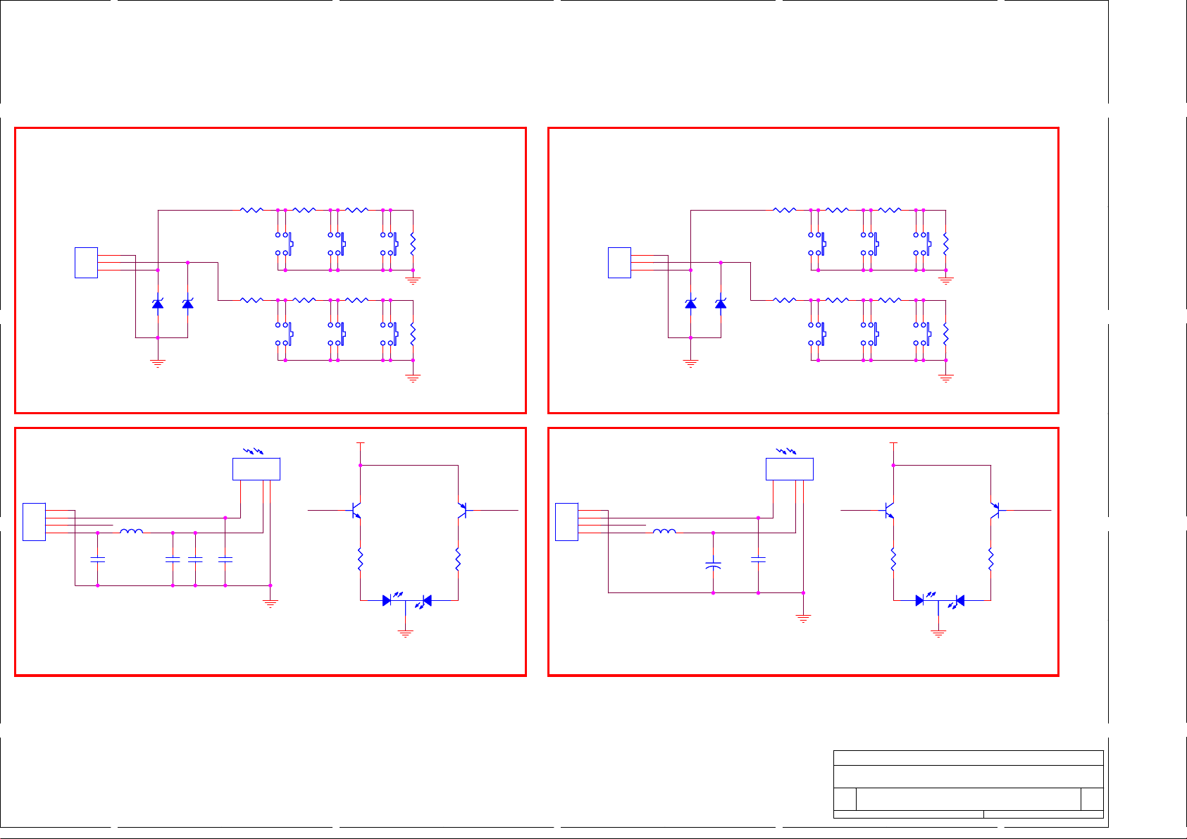
5
A
4
3
2
1
D D
K1001:CH+
K1002:CHK1003:VOL+
R1001
R1001
1.2K
1.2K
P1001
P1001
3
KEY1
2
KEY0
1
D1002
D1002
D1001
5.6HSB
5.6HSB
D1001
5.6HSB
5.6HSB
CON6_2.0
CON6_2.0
C C
R1005
R1005
1.2K
1.2K
M61 KEY BOARD结构
G1001
G1001
321
AT156BS
C1004
C1004
10uf
10uf
C1002
C1002
0.1uf
0.1uf
AT156BS
C1001
C1001
22pF
22pF
P1001
P1001
4
IR IR
3
LED
L1001
5VSTB
C1003
C1003
10uf
10uf
L1001
3.3uH
3.3uH
CON6_2.0
CON6_2.0
2
1
B B
K1004:VOLK1005:MENU
K1006:SOURCE
R1002
R1002
0.4V 0.8V 1.2V
1.5K
1.5K
K1002SWK1002
SW
K1005SWK1005
SW
124
3
124
3
1
124
K1001SWK1001
SW
3
R1006
R1006
0.4V 0.8V 1.2V
1.5K
1.5K
124
K1004SWK1004
SW
3
K1001:CH+
K1002:CHK1003:VOL+
R1001
R10032KR1003
2K
R10072KR1007
2K
K1003SWK1003
SW
K1006SWK1006
SW
124
R1004NCR1004
NC
3
124
R1008NCR1008
NC
3
P1001
P1001
CON6_2.0
CON6_2.0
3
KEY1
2
KEY0
1
D1002
D1002
D1001
D1001
5.6HSB
5.6HSB
5.6HSB
5.6HSB
R1001
1.2K
1.2K
R1005
R1005
1.2K
1.2K
E62 KEY BOARD结构
5VSTB 5VSTB
P1001
P1001
LEDLED
1
3 2
R10111KR1011
1K
13
CON6_2.0
CON6_2.0
4
3
LED
L1001
5VSTB
L1001
3.3uH
3.3uH
C1002
C1002
+
+
47uF/16V
47uF/16V
2
1
2 3
Q1001
Q1001
3904
3904
R10101KR1010
1K
D1001D1001
Q1002
Q1002
3906
3906
AT156BS
AT156BS
C1001
C1001
22pF
22pF
G1001
G1001
321
K1004:VOLK1005:MENU
K1006:SOURCE
R1002
R1002
0.4V 0.8V 1.2V
1.5K
1.5K
K1002SWK1002
SW
K1005SWK1005
SW
124
3
124
3
1
124
K1001SWK1001
SW
3
R1006
R1006
0.4V 0.8V 1.2V
1.5K
1.5K
124
K1004SWK1004
SW
3
R10032KR1003
2K
R10072KR1007
2K
K1003SWK1003
K1006SWK1006
Q1001
Q1001
1815
1815
2 3
SW
SW
R10101KR1010
1K
124
R1004NCR1004
NC
3
124
R1008NCR1008
NC
3
LEDLED
1
3 2
R10111KR1011
1K
13
D1001D1001
Q1002
Q1002
1015
1015
M61 IR BOARD结构
2
E62 IR BOARD结构
2
A
Title
Title
Title
<Title>
<Title>
<Title>
Size Document Number Rev
Size Document Number Rev
Size Document Number Rev
Custom
Custom
Custom
Date: Sheet of
Date: Sheet of
Date: Sheet
IR&KEY ?
IR&KEY ?
IR&KEY ?
of
10 10Monday, June 04, 2007
10 10Monday, June 04, 2007
10 10Monday, June 04, 2007
Page 68

Power Logic Sequence
P2
GND 4
GND 3
12V 2
inverter 24v
U1/U2
12V-AMP
5Vstb
Power Supply Unit
U10 U11
EEPROM
1
5V
U6 regulator
U7
3.3V 1.8V
U8
CPU/DECODER/
SCANNER
on/off panel on/off
on-pback
Panel
5v
Description:While the power cord plug in, the TV is in
standby situation,power supply unit provide 5Vstb 200mA for
load.There is no 12v amplifier power supply and 24V
inverter voltage supply. The 5Vstb through D7 and regulator
U5 get 3.3VA supply for IC (MST19E),the another path of
circuit is 5Vstb through regulator U6 get 3.3V then
regulated by U7(regulator) get 1.8V supply for
U8(MST19E),drive the LED lighting,and standby circuitry
working,and CPU controlling,reset circuitry,crystal.So that
it makes the CPU can receive and send kinds of command.
while there is turn on command(low level) send out from
Pin150 of U8(MST19E),power supply unit provide 12V and 24V
voltage.12V voltage supply for U1/U2,change to 5V voltage,
regulate by U6, change to 3.3V supply for U8 others
parties. 24V voltage supply for inverter board of Panel.
Page 69

YN
check 3 control
voltages(power-
on/off,panel-on/off,on-
pback,) if OK,
NY N
No Working
LED if Lighting
check 5vstb voltage
if OK
check
relevant
circuitry
check working conditions of U8 if OK
I2C BUS
wokring if
OK
U10/U11 power supply and
SCL/SDA
Power supply if
OK
Fig1. No Working
Check the relevant
circuitry,e.g.U6
crystal/Reset
circuitry working if
OK
Page 70

Check
relevant
signal
channel
Defect Picture
Check LVDS
interface
assembly if OK
check if all
signal resources
have defect
picture
all signal channel defect
remove off the LVDS line, if the
defect picture still have
YN
replace the panel
check RP1 to RP7 and
LVDS line or connector
Fig2. Defect Picture
Page 71

No Picture
AV input if have picture
NY
check P4 if assemble
regular
YYN
check Q2,Q3,Q4 and
relevant if regular
YYN
Check Pin 155 and
Pin156 of U8 if output
regular and test the
working conditions of
U8
YY
replace U8
Test waveform of Pin49
of U8 if regular
Replace
U8
check waveform of L28
if regular
check
waveform
of L28 if
regular
replace Tuner
Check the
work
conditions
of Tuner
if OK
Fig3. No Picutre
Page 72
Picture Good,but No Sound
increase the volume and press the
mute key on remote control
test waveform of Pin4 and Pin12 of
U19 if OK
YN
Test waveform of
Pin1,Pin2,Pin15 and
Pin16 if OK
YN YN
Check the
speakers
if Pin3,Pin13,Pin17and
Pin22 no voltage or low
voltage,check relevant
circuitry
Fig4.Picture OK, but No Sound
Check the power supply
voltage and mute control
circuitry if regular
Check voltage
of Pin6 of U19
and Q22 and
relevant
test waveform of
Pin54/Pin55 of U8 if
regular
Check
Replace
U8
Tuner and
R220 and
L29,C181
 Loading...