

Page 1

TCL
SERVICE MANUAL
L32B2810/MT31BP-AP
1. Caution…………………………………………………………………………2
2. specification……………………………………………………………………6
3. Alignment Procedure…………………………………………………………7
4.Block diagram…………………………………………………………………1
5.Scheme Diagram ……………………………………………………………
6. Troubleshooting………………………………………………………………2
([SORGHGUDZLQJ
This m anual i s t he l atest at t he t ime of pr inting, and doe s not
include the modification which may be made after the printing, by
the constant improvement of product
Page 2

RISK OF ELECTR IC
SHOCK DONNOTNOPEN.
1. CAUTION
CAUTION:
Use of controls, adjustments or procedures other than those specified herein may result in
hazardous radiation exposure.
CA UTION : TO RE DUCE THE RIS K OF
CA U T IO N
K
O K
The lighting flash with arrowhead symbol, with an equilateral triangle is intended to
alert the user to the presence of uninsulated voltage within the product s
enclosure that may be of sufficient magnitude to constitute a risk of electric shock to
the person.
The exclamation point within an equilateral triangle is intended to alert the user to the
presence of important operating and maintenance (servicing) instructions in the
literature accompanying the appliance.
ELECTR ICAL SH OCK, DO NOT REMOVE
COVER (OR BACK). NO USER SERVICEABLE
PAR TS INS IDE . RE FER SER VIC ING TO
QUALIFIE D SERVIC E PERS ONNEL.
dangerous
WARNING: TO REDUCE RISK OF FIRE OR ELECTRIC SHOCK, DO NOT
EXPOSE THIS APPLIANCE TO RAIN OR MOISTURE.
2
Page 3

IMPORTANT SAFETY INSTRUCTIONS
CAUTION:
Read all of these instructions. Sa ve these instructions for later use . Follo w all Warnings and
Instructions marked on the audio equipment.
1. Read Instructions-All the safety and operating instructionsshouldbe read before the productis operated.
2. Retain Instructions- The safety and operating instructions should be retained for future reference.
3. Heed Warnings- All warnings on the product and in the operating instructions should be adhered to.
4. Follow Instructions- All operating and use instructions should be followed.
FOR YOUR PERSONAL SAFETY
1. When the power cord or plugis damaged or frayed, unplug this television set from the wall outlet and refer servicing to
qualified service personnel.
2. Do not overload wall outlets and extension cords as this can result in fire or electric shock.
3. Do not allow anything to rest on or roll over the power cord, and do not place the TV where power cord is subject to
traffic or abuse. This may result in a shock or fire hazard.
4. Do not attempt to service this television set yourself as opening or removing covers may expose you to dangerous
voltage or other hazards. Refer all servicing to qualified service personnel.
5. Never push objects of any kind into this television set through cabinet slots as they may touch dangerous voltage
points or short out parts that could result in a fire or electric shock. Never spill liquid of any kind on the television set.
6. If the television set has been dropped or the cabinet has been damaged, unplug this television set from the wall outlet
and refer servicing to qualified service personnel.
7. If liquid has been spilled into the television set, unplug this television set from the wall outlet and refer ser vicing to
qualified service personnel.
8. Do not subject your television set to impact of any kind. Be particularly careful not to damage the picture tube surface.
9. Unplug this television set from the wall outlet before cleaning. Do not use liquid cleaners or aerosol cleaners. Use a
damp cloth for cleaning.
10.1. Do not place this television set on an unstable cart, stand, or table. The television set may fall, causing serious injury
to a child or an adult, and serious damage to the appliance. Use only with a car t or stand recommended by the
manufacturer, or sold with the television set. Wall or shelf mounting should follow the manufacturer s instructions, and
should use a mounting kit approved by the manufacturer.
10.2. An appliance and cart combination should be moved with care. Quick stops, excessive force, and uneven surfaces
may cause the appliance and cart combination to overturn.
3
Page 4
PROTECTION AND LOCATION OF YOUR SET
11. Do not use this television set near water ... for example, near a bathtub, washbowl, kitchen sink, or laundry tub, in a
wet basement, or near a swimming pool, etc.
Never expose the set to rain or water. If the set has been exposed to rain or water, unplug the set from the wall
outlet and refer servicing to qualified service personnel.
12. Choose a place where light (artificial or sunlight) does not shine directly on the screen.
13. Avoid dusty places, since piling up of dust inside TV chassis may cause failure of the set when high humidity persists.
14. The set has slots, or openings in the cabinet for ventilation purposes, to provide reliable operation of the receiver, to
protect it from overheating. These openings must not be blocked or covered.
Never cover the slots or openings with cloth or other material.
Never block the bottom ventilation slots of the set by placing it on a bed, sofa, rug, etc.
Never place the set near or over a radiator or heat register.
Never place the set in enclosure, unless proper ventilation is provided.
a built-in
PROTECTION AND LOCATION OF YOUR SET
15.1. If an outside antenna is connected to the television set, be sure the antenna system is grounded so as to provide some
protection against voltage surges and built up static charges, Section 810 of the National Electrical Code, NFPA No.
70-1975, provides information with respect to proper grounding of the mast and supportingstructure, grounding of the
lead-in wire to an antenna discharge unit, size of grounding conductors, location of antenna discharge unit, connection
to grounding electrode, and requirements for the grounding electrode.
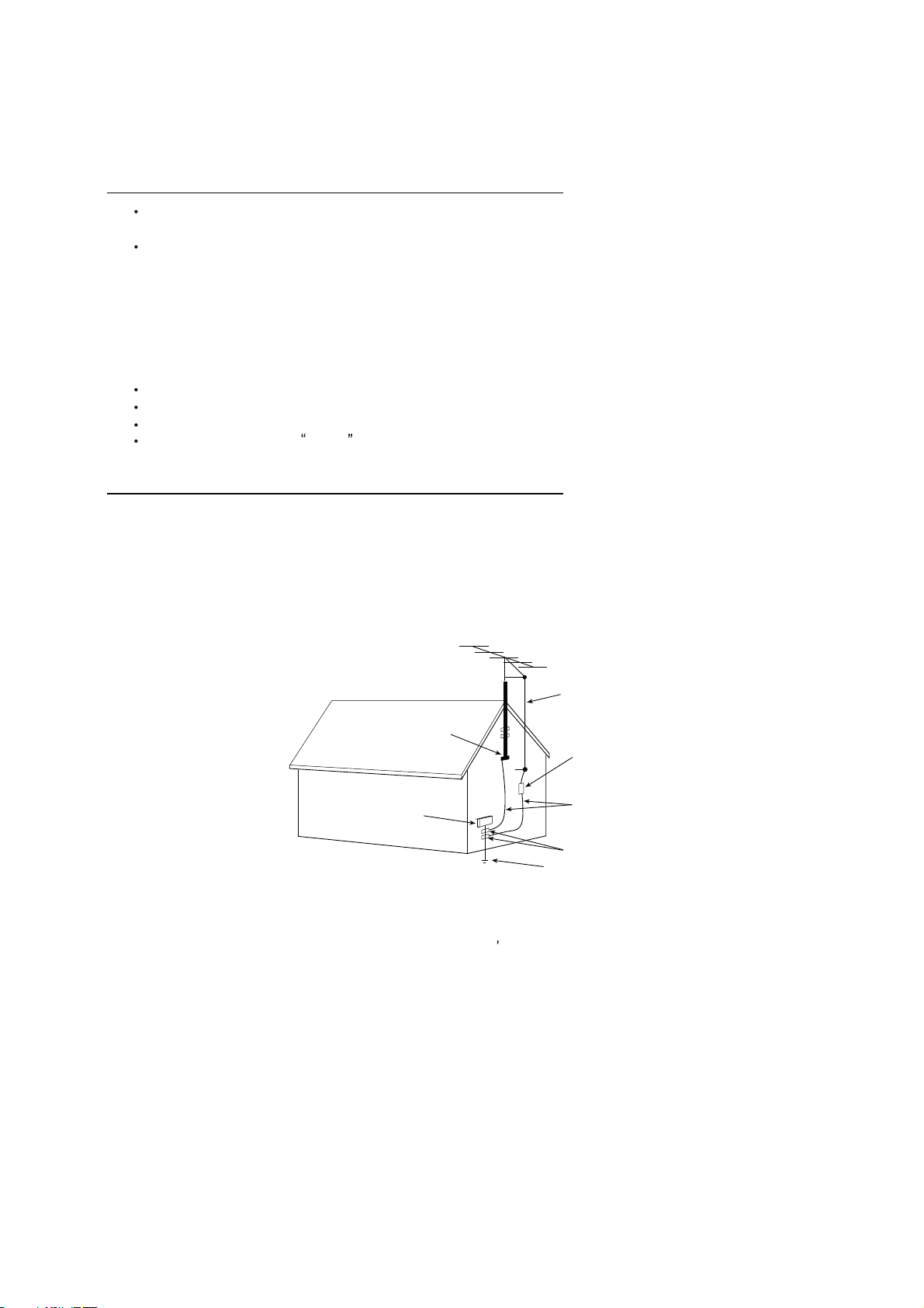
EXAMPLE OF ANTENNA GROUNDING AS PER NATIONAL ELECTRICAL CODE INSTRUCTIONS
EXAMPLE OF ANTENNA GROUNDING AS PER
NATIONAL ELECTRICAL CODE
ANTENNA
LEAD IN WIRE
GROUND CLAMP
ELECTRIC SERVICE
EQUIPMENT
NEC NATIONAL ELECTRICALCODE
ANTENNA DISCHARGE
UNIT (NEC SECTION
810 20)
GROUNDING
CONDUCTORS
(NECSECTION 810 21)
GROUND CLAMPS
POWER SER VICE GROUNDING
ELECTRODE SYSTEM
(NEC ART 250 PARTH)
15.2. Note to CATV system installer : (Only for the television set with CATV reception)
This reminder is provided to call the CATV system attention to Ar ticle 820-40 of the NEC that provides
installer s
guidelines for proper grounding and, in particular, specifies that the cable ground shall be connected to the grounding
system of the building, as close to the point of cable entr y as practical.
16. An outside antenna system should not be located in the vicinity of overhead power lines or other electric lights or power
circuits, or where it can fall into such power lines or circuits. When installing an outside antenna system, extreme care
should be taken to keep from touching such power lines or circuits as contact with them might be fatal.
17. For added protection for this television set during a lightning storm, or when it is left unattended and unused for long
periods of time, unplug it from the wall outlet and disconnect the antenna. This will prevent damage due to lightning
and power-line surges.
4
Page 5

OPERATION OF YOUR SET
18.
This television set should be operated only from the type of power source indicated on the marking label.If you are not
sure of the type of power supply at your home, consult your television dealer or local power company. For television
sets designed to operate from battery power, refer to the operating instructions.
19. If the television set does not operate normally by following the operating instructions, unplug this television set from the
wall outlet and refer servicingto qualifiedservice personnel. Adjust only those controls that are covered in the operating
instructions as improper adjustment of other controls may result in damage and will often require extensive work by a
qualified technician to restore the television set to normal operation.
20. When going on a holiday : If your television set is to remain unused for a period of time, for instance, when you go on
a holiday, turn the television set and unplug the television set from the wall outlet.
off
IF THE SET DOES NOT OPERATE PROPERLY
21. If you are unable to restorenormal operation by followingthe detailedprocedurein your operatinginstructions,
do not attempt any further adjustment. Unplug the set and call your dealer or service technician.
22. Whenever the television set is damaged or fails, or a distinct change in performance indicates a need for
service, unplug the set and have it checked by a professional service technician.
23. It is normal for some TV sets to make occasional snapping or popping sounds, particularly when being
turned on or off. If the snapping or popping is continuous or frequent, unplug the set and consult your
dealer or service technician.
FOR SERVICE AND MODIFICATION
24. Do not use attachments not recommendedby the television set manufacturer as they may cause hazards.
25. When replacement parts are required,be sure the service technicianhas used replacementparts specified
by the manufacturer that have the same characteristics as the original part. Unauthorized substitutions
may result in fire, electric shock, or other hazards.
26. Upon completion of any service or repairs to the television set, ask the service technician to perform
routine safety checks to determine that the television is in safe operating condition.
5
Page 6

第 1 页共27 页
TCL 集团多媒体电子全球制造中心
IPC 设计中心
文件编号:IPC/SJ/FK02-2013
序号:
Alignment Procedure
VERSION:V0.92
MM31BP Series
PREPARED BY : ZHANGLI DATE : 2014-05-07
APPROVED BY : DATE :
Page 7

TCL World-Wide R&D
FPD CENTER
Test & Alignment Specification (TAS)
MT31BP-AP 调试说明 (v0 92).docx
for MT5531
EU/AU/RU Series
Version 0.92
Î MT31L: Low Cost CCFL & LED Platform
Î MT31D: Low Cost CCFL & LED Platform (for E3000 ID only)
Î MT31B:Basic Entry Level LED Platform
Î MT31BT/LT/DT: DVB-T2 Chassis LED Platform
Î MT31BS/LS: DVB-S2 Chassis LED Platform
Î MT31LB: DVB-T2 Chassis LED Platform for TOT
MT31LB: Add MT31BP information of LCD
Page 1 of 26
Page 8

MT31BP-AP 调试说明 (v0 91).docx
Disclosure
The information contained in this document is proprietary to TCL SZ FPD lab and shall not be disclosed by
the recipient to third persons without the written permission of the team leader or GM of R&D.
Revision History
Version Issue Date Description of changes
This is 1st Draft version
v0.10
v0.20
2013-01-06
2013-03-01
· Add MT31B For Entry Level LED
· Add MT31L For Low Cost CCFL & LED Platform
· Add MT31D For Low Cost CCFL & LED Platform base on E330
·Improve header information on MT5531
.Change Power Mode to Boot
v0.30
v0.40
v0.50
v0.60
v0.70
v0.80
v0.90
2013-03-18
2013-04-12
2013-04-18
2013-04-23
2013-05-23
2013-06-11
2013-07-12
. Delete offsets: +0.002 for “x” and +0.012 for “y
. Add Project White Balance Information
. Add MAC upgrade method by USB
. Upgrade MTK Tool for MT31.
. Mr.Christian upgrade information
.Add PQ engineer Note information
.Add project White Balance Information
.Add HDCP upgrade method.
.WB adjust need to fix default G Gain
.The signal level check has been down in R&D, Factory should not adjust the
scaling Brightness , scaling contrast and scaling saturation.
.Add MT31BT/LT/DT DVB-T2 function chassis;
.Add MT31BS/LS S2 DVB-S2 function chassis
.Add AU/RU Market project information
.Improve MT31 function information for EU / AU / RU
.Add EU/AU project white balance information
.Add project White Balance Information
.Add project White Balance Information
V0.91
V0.92
2013-09-02
2014-05-07
Add MT31LB DVB-T2 for TOT information.
Add MT31BP information of LCD
Page 2 of 26
Page 9
MT31BP-AP 调试说明 (v0 91).docx
These chassis are designed for European LCD TV markets with MPEG4 for both TCL/THOMSON brands. The
main chip is from Mediatek (MT5531 series) and support below feature matrix:
Class Item
MT31B/L/D MT31BT/LT/DT MT31BS/LS MT31B/L/D MT31LB
Input ATV
EU AU RU
( PAL B/G D/K I,
&
Output DTV
SECAM B/G D/K
L/L)
MPEG-2, MPEG-4 DVB-T2 DVB-S2 DVB-T2
HDMI - CEC
(480i/p, 576i/p,
720p up to
1080i/p, compliant
v1.4a with HDCP)
VGA
VGA/CMP audio
CMP
(YPrPb can
support from 480i
up to 1080p,
audio)
√ √ √ √ √
DVB-T/C DVB-T/C DVB-T/C DVB-T/C DVB-T/C
MT31B/D:2
MT31L:1
1 1 1 1 1
1 1 1 1 1
1 1 1 1 1
MT31B/D:2
MT31L:1
MT31B/D:2
MT31L:1
MT31B/D:2
MT31L:1
2
SCART1
(CVBS & RGB
&YC, audio)
Side AV or Back
AV
(CVBS, audio)
USB(2.0)
√ √ √ N/A N/A
N/A N/A N/A 1 N/A
1 1 1 1 1
Picture,
Video,
Audio
Playback
Picture, Video,
Audio Playback
Picture,
Video,
Audio
Playback
Picture,
Video,
Audio
Playback
Picture, Video,
Audio Playback
Page 3 of 26
Page 10
MT31BP-AP 调试说明 (v0 91).docx
Functions
SCART1 output
(CVBS, audio)
AV output
(RCA)
(CVBS, audio)
Headphone
output
SPDIF output
RJ-45
MEMC
OAD
CI+1.3
WIFI Ready
DIVX
DLNA (DMP)
√ √ √ N/A N/A
N/A N/A N/A √ N/A
√ √ √ √ N/A
Coaxial Coaxial Coaxial Coaxial Coaxial
IP Return IP Return IP Return N/A N/A
N/A N/A N/A N/A N/A
√ √ √ √ √
√ √ √ N/A √
N/A N/A N/A N/A N/A
N/A N/A N/A N/A √
N/A N/A N/A N/A N/A
Internet
Audio Return
Channel
Serial connector
VGA connector
Others
I2C connector of
MEMC module
N/A N/A N/A N/A N/A
√ √ √ √ √
N/A N/A N/A N/A N/A
P1000 P1000 P1000 P1000 P1000
N/A N/A N/A N/A N/A
Class Item MT31B MT31L MT31D
IC Details
&
Position
Main SW BIN image
(NOR 64Mb Flash)
System Memory
HDMIx Switch
EDID BIN image
VGA
EDID BIN image
U702 U702 U702
Integrated to Flash Integrated to Flash Integrated to Flash
Embedded to SoC
at Firmware On-Power
at Firmware On-Power at Firmware On-Power
Embedded to SoC
at Firmware On-Power
Embedded to SoC
at Firmware On-Power
at Firmware On-Power
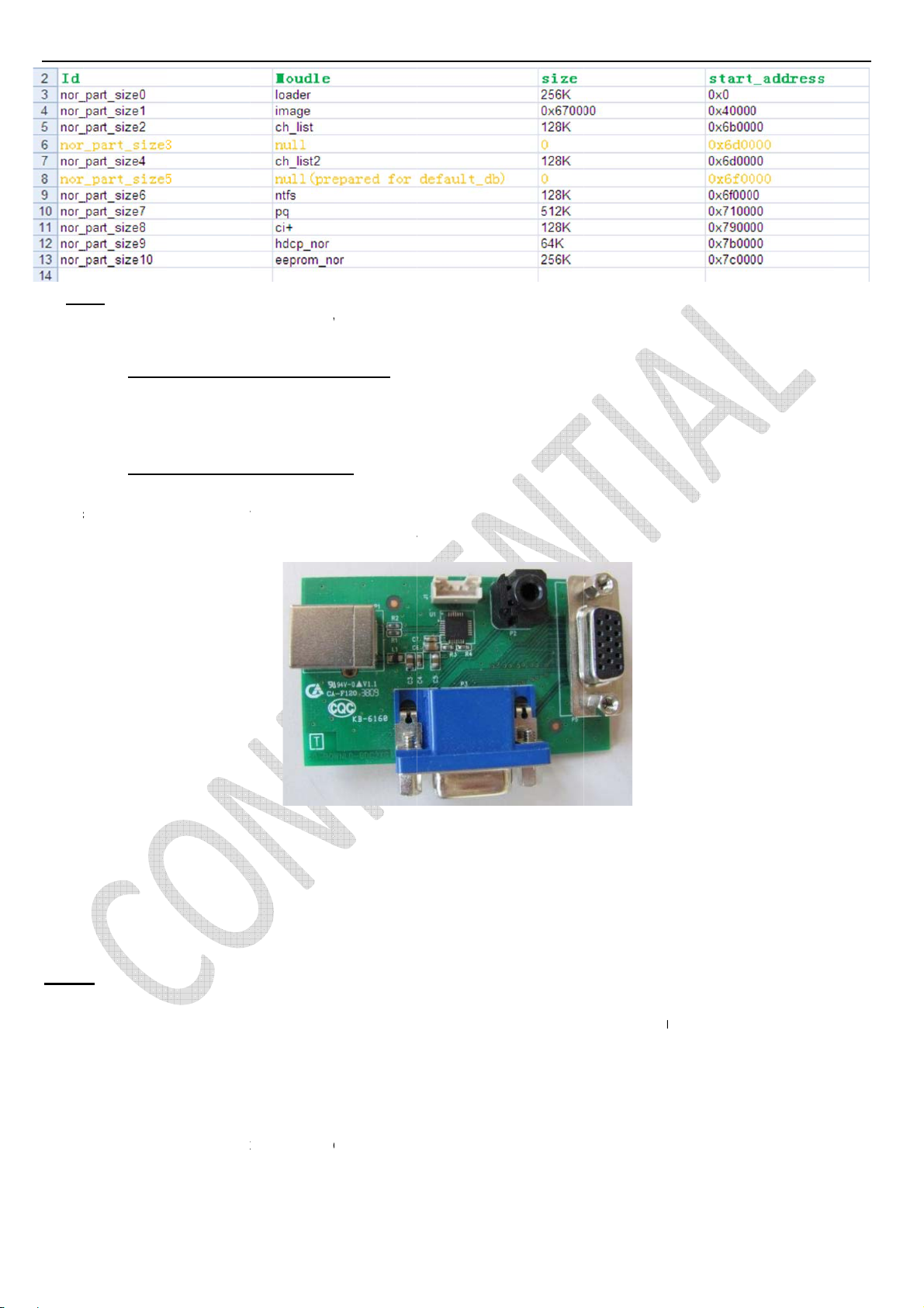
·MT5531 FLASH Size and Key Blocks Location’s Assignment
Page 4 of 26
Page 11
o
c
O
e
r
y
u
e
m
a
e
u
m
l
C
R
r
r
o
e
o
a
t
e
M
w
s
t
e
s
e
h
t
e
PPw
e
d
h
4
(
d
1
n
c
e
C
e
x
e
s
r
o
a
s
a
e
d
O
t
c
m
t
S
g
e
e
a
a
4
C
N
It i
VGA
To
te:
s necessar
Man
/ P1000
USB
ommunicat
to erase F
facturing
Pin4:
to UART B
with TV p
like foll
ash before
onnector
XD Pin11
idge Adap
oduct for d
wing snap
T31BP-A
riting cod
Pinout
:TXD
er (Silicon
bugging, a
hot (further
调试说明
file for rea
Labs CP2
justment a
details are
v0 91).doc
ing in corr
0 chipset
d so… it’s
described
ctly EEPR
eries)
equired sui
n below se
M data.
able 0..5V
tions):
erial Interf
ce
INF
ª All
VAC)
ª All
ª All
ª Th
perfo
influe
:
tests and
voltages h
final tests h
Picture P
med into s
nce (colori
easuremen
ve to be m
ave to be d
rformance
bdued ligh
etry vs tim
ts mention
asured wit
ne on a co
ssessmen
ed room aft
)
d hereafter
respect to
mplete set i
such as W
r at least
have to be
ground, unl
ncluding L
ite Balanc
5min of wa
arried out
ss otherwi
D panel in
(luminanc
rm-up in or
t a normal
e stated
room with
and color
er to avoid
mains volta
temperatur
emperatur
any temper
e (220 ~ 2
of 25+/-7°
) has to be
ture drift
0
age 5 of 26
Page 12

MT31BP-AP 调试说明 (v0 91).docx
1. PCB/SKD Assembly: Test & Alignment
1.1. Pre-Conditions and DC/DC Check
Before power on, please check the board according to the relevant block diagram and circuit diagram, and
make sure that no serious issue or mistake can destroy the board. For example, the output of DC/DC and
LDO should not be shorted to ground.
Supply a suited voltage and power-on, then check the voltage according to the relevant block diagram,
circuit diagram and voltage specification within 5% margin.
For example, check SoC voltage (AV3V3, VCCK-1V2, etc.), DDR voltage (DDRV) , amplifier voltage
(Main_Power), etc… Only the standby voltage is necessary if there is no software in the flash.
SW Image download
1.2.
Download the latest release SW from below FTP server:
- Link:xxxxx
- Username: xxxxx
- Password: xxxxx
- Folder: xxxxx
See Appendix
See Appendix
OAD Transport Stream Image
To manage quicker mass reflashing, a predefined OAD DVB-T channel (freq:850MHz / bandwidth:8MHz) is
embedded to SW core and only available into Factory mode. Some licensed IBL tools ('xxx2lli.exe', 'lli2dsm.exe',
dsmmerge.exe, …) from Intellbyte Inc. (http://www.intellibyte.com/
SSU TS. Over some predefine settings such as repeated datablock insertion, null packets size, … (controllable in
configuration file), here below are mandatory OUI entries structure to prepare DSM-CC carousel image format:
⑴ “How to upgrade FLASH SW using MTK tool”
⑵ “How to upgrade FLASH SW using USB”
) might be necessary to create appropriate DVB
OUI Entry MT31L MT31B MT31LB
CUST_OAD_OUI
CUST_OAD_HW_MODEL
CUST_OAD_HW_VERSION
CUST_OAD_SW_MODEL (x) 0x3101 0x3102 0x3102
CUST_OAD_SW_VERSION (yyy) 0x0xxx 0x0xxx 0x0xxx
Note ⑴: SW Entry are referring to following PKG image file name “V8-0MT310x-LF1Vyyy.pkg”
⑵
Note
: See enclosed necessary Data Broadcast Carousel configuration file format det ails (DBC)
408BF6 408BF6 408BF6
0x5881 0x5881 0x5881
0x0001 0x0001 0x0001
Page 6 of 26
Page 13

TCL_HW5881.pdf
MT31BP-AP 调试说明 (v0 91).docx
To build an OAD TS, it’s necessary to create a temporary common and interchangeable DSM file format using
below command and arguments:
‘bin2dsm.exe -v -v -v -m0,0,"TCL_HW5881",0 -n200 -z102400 -nz -o%FILE%.dsm -h"OUI=CUST_OAD_OUI
model=CUST_OAD_HW_MODEL version=CUST_OAD_HW_VERSION vm=0xffff" -s"OUI=CUST_OAD_OUI
model=CUST_OAD_SW_MODEL version=CUST_OAD_SW_VERSION vm=0xffff" %FILE%.pkg’
Then, OAD TS can be completed using below command and arguments:
‘dsmsectn.exe -v -dvbssu -mpegts -patpmt -nit_ter -sdt -o%FILE%.ts -gTCL_HW5881.dbc %FILE%.dsm’
For more robustness, TS can be played with following presets such as modulation:QAM-64, guard interval:1/8,
coding rate:2/3 to ensure ~22Mbps.
OAD reflashing process is managed within 4 steps operation: multiplex detection, DVB transfer, flashing and
warm-start.
See Appendix
⑶ “How to upgrade FLASH SW using OAD”
UART & IR Parser
1.3.
To use both UART and/or IR parser, TV has to be set in Factory mode with its VGA port well connected to
suitable UART device or an IR emitter device correctly facing up TV (see below “Product Assembly - section 2.0”
how to activate “Factory key”).
The SoC’s RS232 mode is automatically enabled at power-on and doesn’t require any command initialization
frame. <0x30 0x30 0x30 0x2E 0x30 0x65 0x30 0x74 0x30 0x0D 0xE2> from host to TV.
So correctly setup UART parser engine for further serial communication, it’s necessary to send following
command frame <0xAA 0x06 0x10 0x01 0xA7 0xEF> within following COM presets 115200/8/n/1; “PS” caption
might be toggled and displayed on bottom left screen (“S” like Serial) if successfull.
To communicate with TV depending on SIACP revision layout implementation, you may need to fulfill UART/IR
commands protocol and format described on enclosed SIACP requirements document (rev. v5.9).
SIACP_V5.9.pdf
1.4. ProjectID Modification
There are different IDs stored into system memory depending on different Panels settings and Models features,
but there’s only one key branching ProjectID that includes all. So, it’s not recommended to modify PaneID with
Hyper terminal as other ID features may not change!
To modify ProjectID, you need to go through “Factory menuÆOtherÆProject infoÆProject ID”, then spin left
or right with RCU “◄/►” key” keys to suitable ID (Project name is dynamically refreshed).
See Appendix
⑷ “How to change ProjectID with RCU”
Page 7 of 26
Page 14
MT31BP-AP 调试说明 (v0 91).docx
Here below is none exhaustive ProjectID table for reference. Project list and all relative information are
dispatched and updated as a new firmware package is released.
Project Name Project ID Panel
32T3520 配 MT31BP 项目 109
32B2800 配 MT31BP 项目 110
32B2610S 配 MT31BP 项目 111
32B2600 配 MT31BP 项目 108
32B2500B 配 MT31BP 项目 112
23E4200 配 MT31BP 项目 113
24T3520 配 MT31BP 项目 114
24B2500 配 MT31BP 项目 115
28T3520 配 MT31BP 项目 116
28B2500B 配 MT31BP 项目 107
24B2800 配 MT31BP 项目 117
32T3520 配 MT31BP 项目 109
PANEL_CS2_ST3151A04
PANEL_CS2_ST3151A04
PANEL_CS2_ST3151A04
PANEL_CS2_ST3151A04
PANEL_CS2_ST3151A04
PANEL_SS_LSC230AN0
PANEL_AUO_M240HTN01
PANEL_CM5_V236BJ1_P03
PANEL_CS5_ST2751A01
PANEL_CS5_ST2751A01
PANEL_CM1_ V236BJ1_LE2
PANEL_CS2_ST3151A04
1.5. Functional Test
Once the boards (chassis, KB, IR, PSU…) and the panel are well interconnected, plug all suitable signals
generator to relevant below inputs/outputs using respective test patterns format to check picture/sound quality:
Source Test Signal Test Pattern
Analog /Digital Tuner
(VHF/UHF & CATV)
Satellite Tuner
(only for MT31BS)
- DiSEqC v1.0 (A, B, C, D) and Tone
Burst (A, B)
- Double LNB frequency (band change
by 22KHz Tone)
RF cable generator
Compliant DVB-S/S2
source from generator or
dish antenna with switch
2D - Movie 1280x720
2D - Static Picture 1920x1080
1. Frequency Range: full band
2. Standard: PAL / SECAM
3. DVB-T/C DVB-T2
2D - Movie 720x576
1. Frequency Range: 950MHz..2150MHz
2. Symbol Rate Range:
DVB-S 1..30MHz (for QPSK)
DVB-S2 1..45MHz (for QPSK)
1..30MHz (for 8PSK)
3. LNB Voltage Range:
Vertical 12.85V..14.2V
Horizontal 17.6V..19.5V
4. 22KHz Tone Range
Frequency 20.5KHz..23.5KHz
Amplitude 400mV..900mV
Current ≥400mA
Page 8 of 26
Page 15

MT31BP-AP 调试说明 (v0 91).docx
SPDIF (optical / cinch)
PCMCIA
SCART/AV IN via adaptor on MT31B/T
(CVBS & RGB & S-VIDEO)
SCART/AV OUT via adaptor on
MT31B/T
(CVBS & Audio out)
PC
(VGA)
CMP via mini jack adaptor on MT31B/T
(YPrPb & Audio)
HDMI
RJ-45
Headphone
Loud Speakers / Enclosures
Suitable Audio Amplifier PCM or Dolby D+
CI CAM card adaptor Conax, Irdeto, Viaccess, …
Chroma/Fluke generator
Monitor Suitable channel
Chroma/QuantumData
generator
Chroma/QuantumData
generator
Video & Audio with beyond
HDMI 1.4a and HDCP
compliant DVD/BD player
MHL up to 720p
ARC PCM or Dolby D+
CEC
IP Return N/A
RF signal N/A
RF signal Suitable channel
PAL Half Color & Gray bars 720x576
Half Color & Gray bars
WXGA - 1368x768@60Hz
Half Color & Gray bars
1920x1080i@60Hz
Half Color & Gray bars
2D - Movie 1920x1080@p24Hz
One Touch Play/ Routing Control/ Sys Standby/
Sys Info/ Give Device Power Status/ Pass
Through/ System Audio Control/
Audio Return Channel
Picture/Video formats and Audio tones can be changed by the factory according to their own standard and
broadcasted signals (ie: 1KHz & 3KHz, sweep, …).
1.6. AD Calibration Test
N/A
As SoC as built-in A/D self-calibration mechanism, there’s not any ADC to perform.
1.7. DDC & EDID & T-Link Test
The E-EDID data structures are according to VESA Enhanced EDID 1.4a (and EIA/CEA-861B for HDMI)..
All VGA and HDMI structures have their own BIN profile which are part of firmware and uploaded at power-on.
For EDID check, it’s recommended to check whether the correct EDID is uploaded by checking corresponding
EDID NVM Checksum or read them out to check bit by bit if it is in line with the released EDID bin file.
1.8. HDCP Upgrade and Test
See Appendix ⑸ “How to upgrade HDCP KEY by UART”
For HDCP compliancy, it’s needed to check whether the HDCP key has been well set by connecting suitable
generator signal.
Page 9 of 26
Page 16

MT31BP-AP 调试说明 (v0 91).docx
1.9. CI+ Key Upgrade, Activation and Test
See Appendix
See Appendix
⑹ “How to upgrade and activate CI Key using USB”
⑺ “How to upgrade and activate CI Key using MTK tool”
1.10. IP Return Test
Appendix ⑻ “How to upgrade MAC address using USB”
All MT31 series platform support IP return function according to CI+ v1.3.
Here are some representative code example:
Note:
Testing method is under completion.
MAC Address
40-8B-F6-90-4D-53
2. Product Assembly (PA): Test and Alignment
2.1. Factory Menu
Follow the below steps to pop-up the Factory menu in case of “FactoryKey” is disabled:
- Press RCU “MENU” key to display main menu
- Select “Picture” and press “OK” key to enter into Picture submenu
- Scroll down to “Contrast” item
- Press the subsequence RCU keys “9”, “7”, “3” and “5”
In case of “FactoryKey” is enabled, just press RCU “Return” key to pop-up again the Factory menu.
The status of “Factory Key” can be changed in “Factory Menu->Hotkey”
Press RCU “OK/►” key to enter the submenu.
Press RCU “Menu” key to go back to the root menu.
Press RCU “◄/►” key to change the values.
Press RCU “OK” key run the function.
Press RCU “Exit” key exit the Factory menu.
Factory Captions Description
Page 10 of 26
Page 17

MT31BP-AP 调试说明 (v0 91).docx
While “FactoryKey” is enabled, there’re some toggled display informations (~2s) relative to SW, ProjectID, CI+,
NetworkID to facilitate 100% quick screening without accessing to whatever else menu:
Î Firmware Version (MV) - ‘V8-0MTxxxx-LF1Vyyy’
Î Project ID (ID) - range [000..999]
Î CI Key Activation flag (CI+) - ‘NO’= no key, ‘YES’= key activated
Î HDCP Key (HDCP) - ‘NULL’= no key, ‘YES’= key activated
Î PVR flag (ERG) - ‘OFF’= disabled, ‘ON’= enabled
P (Production/Factory mode flag) / S (Factory UART Parser mode flag) / W (Warm-Up mode flag)
2.2. Channel Map Preset
Region channel Maps are stored in the firmware and can be directly preloaded via Factory menu.
Other faster methods via UART/IR commands are available on enclosed SIACP requirements (rev. v5.9).
See Appendix
⑼ “Factory Menu Description”
2.3. Warm-up Test
Following TCL standard and practices, it’s required minimum 15min of Warm-Up that can be considered as
Burn-In. Additional Aging for White Balance alignment is no more necessary due to consistent Picture Performance
with Cloning usage.
This function is accessible by selecting “Factory menu ÆBurning Mode”, pressing RCU “OK/►” key, to
release/disable Burn-in mode, it’s just required to press “Menu” button from local keyboard. Other faster methods
via UART/IR commands are available on enclosed SIACP requirements (rev. v5.9).
2.4. White Balance (WB) Cloning
White Balance Touch-Up
As some color coordinates discrepancies can be noticed from panel batches to others, it may necessary to
perform slight touch-up.
For Color temperature adjustment, switch TV on leading HDMI input where should be connected suitable
generator providing following format 1280x720p@60Hz test pattern. A 32 steps grey scale is recommended to
assess relevant colorimetry tracking and low/high light saturation points.
(Golden sample)
Page 11 of 26
Page 18

MT31BP-AP 调试说明 (v0 91).docx
Make sure Picture Preset is set to “DYNAMIC” mode, both “Contrast” and “BackLight” bargraph are set to
“100” (maximum), “Gamma” bargraph are set to “0” (2.2 nominal) and that both “Energy Saving” and “Light
Sensor” are set to “Off” from “ECO Settings” subsection.
Ensure that TV is in Factory mode to access to ”White Balance” adjustment submenu, then scroll down to
toggle off “Pic. Enhance” flag.
PC VGA, CMP YPrPb, SCART RGB, CVBS_PAL/SECAM Gain/Offset matrix offsets locations are relative to
HDMI/DTV.
Warm and Cool Tone are relatives to Normal mode. WB adjust need to fix default G Gain .
¾ “Gain” registers set need to be adjusted at 70IRE.
¾ “Offsets”
registers set can be adjusted at 30IRE, but it’s not recommended to keep them defaulted.
Note: All matrix offsets locations can be individually fine-tuned.
Targets and Tolerances for all inputs
Note: The White balance value is right conformed by PQ Engineer , Except PQ Engineer, anybody can
not change the white balance value and Default value.
The measured and adjustable parameters should be mainly “x”, “y” coordinates (see “TCL EU Picture Quality
Requirements for FPDs” for reference).
The signal level check has been down in R&D, Factory should not adjust the scaling Brightness , scaling
contrast and scaling saturation.
The White Balance alignment should be performed using a well calibrated and contact less analyzer (ex:
CA310). The analyzer may not touch the screen surface, and measurement must be performed in a dark
environment keeping the probe(s) at 90+/-2° from the panel center.
The results should fulfill following TCL matching requirements (Minolta CA210-CH00 based):
Area EU White Balance Default
Project Name Bom No. COOL NORMAL WARM COOL NORMAL WARM
L19D3303 H3-19D33S2-WE1A(B)WAA 274,294 283,307 318,350 -3,0,9 128,128,128 16,0,-27 A
L19D3303 H3-19D33S2-WE1CWAA 268,284 278,298 313,339 -3,0,9 128,128,128 16,0,-27 A
19HU5253C H3-19E53S2-EU1C(D)WAA 272,296 282,308 317,347 -3,0,9 128,128,128 16,0,-27 A
19HU5253C H3-19E53S2-EU1A(B)WAA 274,294 283,307 318,350 -3,0,9 128,128,128 16,0,-27 A
19HU5253CW H3-19E53S2-EU1BWAA 274,294 283,307 318,350 -3,0,9 128,128,128 16,0,-27 A
L19E4103 H3-19E41S2-WE1AWAA 290,317 300,330 338,365 -3,0,9 130,124,128 16,0,-27 A
Page 12 of 26
Energy
Efficiency
Page 19

MT31BP-AP 调试说明 (v0 91).docx
19HW4323 H3-19E41S2-WE1BWAA 290,317 300,330 338,365 -3,0,9 130,124,128 16,0,-27 A
19HW4323W H3-19E41S2-WE1CWAA 290,317 300,330 338,365 -3,0,9 130,124,128 16,0,-27 A
L19E4153 H3-19E41S2-WE1DWAA 290,317 300,330 338,365 -3,0,9 130,124,128 16,0,-27 A
L19E4143 H3-19E41S2-WE1EWAA 290,317 300,330 338,365 -3,0,9 130,124,128 16,0,-27 A
L19E4133 H3-19E41S2-WE1FWAA 290,317 300,330 338,365 -3,0,9 130,124,128 16,0,-27 A
L23F3303 H3-23F33S2-WE1AWAA 270,292 280,302 315,336 -3,0,9 128,128,128 16,0,-27 A+
L23F3393 H3-23F33S2-WE1BWAA 270,292 280,302 315,336 -3,0,9 128,128,128 16,0,-27 A+
L24E4103F H3-24E41S2-WE1AWAA 260,275 270,287 305,325 -3,0,9 128,128,128 16,0,-27 A
24FW4323 H3-24E41S2-WE1BWAA 260,275 270,287 305,325 -3,0,9 128,128,128 16,0,-27 A
24FW4323W H3-24E41S2-WE1CWAA 260,275 270,287 305,325 -3,0,9 128,128,128 16,0,-27 A
L24E4153F H3-24E41S2-WE1DWAA 260,275 270,287 305,325 -3,0,9 128,128,128 16,0,-27 A
L24E4143F H3-24E41S2-WE1EWAA 260,275 270,287 305,325 -3,0,9 128,128,128 16,0,-27 A
L24E4133F H3-24E41S2-WE1FWAA 260,275 270,287 305,325 -3,0,9 128,128,128 16,0,-27 A
L24E3500 H3-24E35S2-WE1AWAA 260,275 267,285 305,325
26HW4323 H3-26E41S2-WE1AWAA 262,274 271,287 305,329 -3,0,9 128,128,128 16,0,-27 A
26HW4323W H3-26E41S2-WE1FWAA 262,274 271,287 305,329 -3,0,9 128,128,128 16,0,-27 A
L26E4133 H3-26E41S2-WE1BWAA 262,274 271,287 305,329 -3,0,9 128,128,128 16,0,-27 A
L26E4103 H3-26E41S2-WE1CWAA 262,274 271,287 305,329 -3,0,9 128,128,128 16,0,-27 A
L26E4143 H3-26E41S2-WE1DWAA 262,274 271,287 305,329 -3,0,9 128,128,128 16,0,-27 A
L26E4153 H3-26E41S2-WE1EWAA 262,274 271,287 305,329 -3,0,9 128,128,128 16,0,-27 A
L32F3303 H3-32F33Q9-WE1AWAA 270,280 280,290 315,327 -3,0,9 128,128,131 16,0,-27 A+
L32F3393 H3-32F33Q9-WE1BWAA 270,280 280,290 315,327 -3,0,9 128,128,131 16,0,-27 A+
L32HW3323 H3-32E33S3-WE1DWAA 270,290 278,302 315,340 -3,0,9 123,128,130 16,0,-27 A+
L32E4503 H3-32E45Q9-WE1AWAA 268,286 278,300 314,340 -3,0,9 128,128,128 16,0,-27 A+
LT-32HA48U H3-32E45Q9-WE1BWAA 268,286 278,300 314,340 -3,0,9 128,128,128 16,0,-27 A+
32HU5253C H3-32E33S3-WE1BWAA 268,286 278,300 314,340 -3,0,9 128,128,128 16,0,-27 A+
32HW3323 H3-32E33S3-WE1AWAA 268,286 278,300 314,340 -3,0,9 128,128,128 16,0,-27 A+
L32E3003 H3-32E33S3-WE1CWAA 268,286 278,300 314,340 -3,0,9 128,128,128 16,0,-27 A+
32HU5243C H3-32E53Q9-WE1CWAA 268,286 278,300 314,340 -3,0,9 128,128,128 16,0,-27 A+
32HU5253C H3-32E53Q9-WE1AWAA 268,286 278,300 314,340 -3,0,9 128,128,128 16,0,-27 A+
32HU5253CW H3-32E53Q9-WE1BWAA 268,286 278,300 314,340 -3,0,9 128,128,128 16,0,-27 A+
L32E4503 H3-32E45Q9-WE1AWAA 268,286 278,300 314,340 -3,0,9 128,128,128 16,0,-27 A+
L32E4503 H3-32E45Q9-WE1CWAA 268,286 278,300 314,340 -3,0,9 128,128,128 16,0,-27 A+
L32E5503 H3-32F35Q9-WE1AWAA 266,275 275,286 312,324 -3,0,9 128,128,128 16,0,-27 A+
L32E3020 H3-32E30S3-WE1AWAA 265,282 275,295 314,341
L39F3303F H3-39F33Q9-WE1AWAA 270,280 280,290 315,327 -3,0,9 128,128,128 16,0,-27 A+
L39F3393F H3-39F33Q9-WE1BWAA 270,280 280,290 315,327 -3,0,9 128,128,128 16,0,-27 A+
L39E3003F H3-39E30S3-WE1AWAA 268,265 278,277 313,317 -3,0,9 128,128,128 16,0,-27 A+
39FU3253C H3-39E33S3-WE1AWAA 268,265 278,277 313,317 -3,0,9 128,128,128 16,0,-27 A+
L39E4503F H3-39E45Q9-WE1AWAA 270,276 280,290 315,331 -3,0,9 128,128,128 16,0,-27 A+
LT-39HG48U H3-39E45Q9-WE1BWAA 270,276 280,290 315,331 -3,0,9 128,128,128 16,0,-27 A+
39FU5253C H3-39E53Q9-WE1AWAA 270,276 280,290 315,331 -3,0,9 128,128,128 16,0,-27 A+
39FU5253CW H3-39E53Q9-WE1BWAA 270,276 280,290 315,331 -3,0,9 128,128,128 16,0,-27 A+
.-3,0,
9
-3,0,
136,128,126 16,0,-27 A
128,128,131 16,0,-27 A+
9
Page 13 of 26
Page 20

MT31BP-AP 调试说明 (v0 91).docx
39FU5243C H3-39E53Q9-WE1CWAA 270,276 280,290 315,331 -3,0,9 128,128,128 16,0,-27 A+
L40FW3323 H3-40E33S3-WE1AWAA 270,280 280,290 315,327 -3,0,9 128,128,128 16,0,-27 A+
40FU3253C H3-40E30S3-WE1AWAA 263,276 273,287 310,326 -3,0,9 128,128,128 16,0,-27 A+
L40E3003F H3-40E30S3-WE1BWAA 263,276 273,287 310,326 -3,0,9 128,128,128 16,0,-27 A+
40FW5554 H3-40E55R4-EU1AWAA 261,272 275,291 328,351 -3,0,9 134,128,116 16,0,-27 A
40FW5555 H3-40E55R3-EU1AWAA 255,268 265,278 292,302 -3,0,6 132,128,120 12,0,-12 A
46FU5554C H3-46E53R4-WE1BWAA 263,265 270,275 302,308 0,0,6 128,128,128 8,0,-18 A+
46FU5555CS H3-46E53R3-WE1AWAA 263,265 270,275 302,308 0,0,6 128,128,128 8,0,-18 A+
46FU5554CW H3-46E53R4-WE1AWAA 263,265 270,275 302,308 0,0,6 128,128,128 8,0,-18 A+
46FW5565 H3-46E55R3-WE1AWAA 256,269 264,280 286,302 -2,0,6 131,128,123 10,0,-10 A+
46FW5564 H3-46E55R4-EU1AWAA 261,276 270,285 300,319 -3,0,5 126,128,123 10,0,-17 A+
48FU4243C H3-48F33Q9-WE1AWAA 271,276 280,290 316,327 -3,0,9 128,128,128 16,0,-27 A+
50FU3253C H3-50E30Q9-WE1AWAA 270,271 280,283 316,322 -3,0,9 128,128,128 16,0,-27 A+
55FU4243C H3-55F33Q9-WE1AWAA 264,281 273,292 307,329 -3,0,9 142,128,128 16,0,-27 A+
55FW8785 H3-55V76R3-WE1AWAA 258,278 270,295 322,353 -3,0,9 137,128,124 16,0,-27 A+
55FW6763 H3-55E55R2-WE1AWAA 257,277 267,287 297,317 -4,0,5 138,128,125 13,0,-15 A++
32HW3324 H3-32F15U1-WE1AWAA 270,290 280,302 317,341 -3,0,9 128,128,128 16,0,-27 A+
32HW3323 H3-32E33S3-WE1MWAA
32HU3253C H3-32E33S3-WE1PWAA
L32E3003 H3-32E33S3-WE1NWAA
L32E3005 H3-32E30X1-WE1AWAA 270,290 278,302 315,340 -3,0,9 123,128,130 16,0,-27 A+
32HW3325 H3-32F15X1-WE1AWAA 270,290 278,302 315,340 -3,0,9 123,128,130 16,0,-27 A+
270,290 280,302 317,341 -3,0,9 128,128,128 16,0,-27
270,290 280,302 317,341 -3,0,9 128,128,128 16,0,-27
270,290 280,302 317,341 -3,0,9 128,128,128 16,0,-27
A+
A+
A+
Area AU(澳洲) White Balance Default
Project Name Bom No. COOL NORMAL WARM COOL NORMAL WARM
L32E3020 H3-32E30S9-AACA0AA 265,282 275,295 314,341 -3,0,9 128,128,131 16,0,-27 6 star
L26E4100W H3-26E41T5-AACA0AA 262,274 271,287 305,329 -3,0,9 128,128,128 16,0,-27 4 star
L26E4100G H3-26E41T5-AACB0AA 262,274 271,287 305,329 -3,0,9 128,128,128 16,0,-27 4 star
L26E4100P H3-26E41T5-AACC0AA 262,274 271,287 305,329 -3,0,9 128,128,128 16,0,-27 4 star
L26E4100B H3-26E41T5-AACD0AA 262,274 271,287 305,329 -3,0,9 128,128,128 16,0,-27 4 star
L46E5510FDS H3-46E55R5-AACA0AA 261,276 270,285 300,319 -3,0,5 128,128,125 10,0,-17
L32E3020 H3-32E30S9-AACA0AA 265,282 275,295 314,341 -3,0,9 128,128,131 16,0,-27 5 star
L32E3020(ID51) H3-32E30S9-AACB0AA 270,290 280,302 317,341 -3,0,9 128,128,128 16,0,-27 5 star
L24E4100F H3-24E41T5-AACA0AA 265,278 275,290 310,330 -3,0,9 128,128,128 16,0,-27
Energy
Efficiency
Area IR (伊朗) White Balance Default
Project
Name
Bom No. COOL NORMAL WARM COOL NORMAL WARM
Energy
Efficiency
L46F3500F H3-46F35V3-IRCB0AA 259,271 268,282 302,319 -3,0,9 139,128,129 16,0,-27
L32F3500 H3-32F35V3-IRCD0AA 278,285 286,296 319,330 -3,0,9 127,128,134 16,0,-27
L32F3520 H3-32F35V3-IRCC0AA 278,285 286,296 319,330 -3,0,9 127,128,134 16,0,-27
L40F3500F H3-40F35V3-IRCB0AA 272,292 282,302 316,336 -3,0,9 128,128,128 16,0,-27
L28E3500 H3-28E35W4-IRCA0AA 270,288 280,298 316,335 -3,0,9 128,128,115 16,0,-27
Page 14 of 26
Page 21

MT31BP-AP 调试说明 (v0 91).docx
1
Area RU (俄罗斯) White Balance Default
Project Name Bom No. COOL NORMAL WARM COOL NORMAL WARM
L32E5300(俄罗斯) H3-32E53T4-AACA0AA 270,290 280,300 315,335 .-3,0,9 128,128,128 16,0,-27
L39E5300F(俄罗斯) H3-39E53U3-UR1A0AA 260,280 270,288 305,325 .-3,0,9 137,128,128 16,0,-27
L28T3540(俄罗斯) H3-28T354NKI-SC0 275,289 285,298 320,335 -5,0,12 130,128,138 12,0,-10
L24B2520(俄罗斯)
L23E4200(俄罗斯) H3-DE420NTW-SC0 275,289 285,298 320,335 -5,0,12 130,128,138 12,0,-10
L24T3520(俄罗斯) H3-YT352NTW-SC0 275,289 285,298 320,335 -5,0,12 130,128,138 12,0,-10
L24B2800(俄罗斯) H3-YB280NTW-SC0 275,289 285,298 320,335 -5,0,12 130,128,138 12,0,-10
L32B2600(俄罗斯) H3-HB260NTW-SC0 275,289 285,298 320,335 -5,0,12 130,128,138 12,0,-10
L28T3520(俄罗斯) H3-28T352NTW-SC0 275,289 285,298 320,335 -5,0,12 130,128,138 12,0,-10
L32T3520(俄罗斯) H3-HT352NTW-SC0 275,289 285,298 320,335 -5,0,12 130,128,138 12,0,-10
L32B2500B(俄罗斯) H3-HB250NTW-SC0 275,289 285,298 320,335 -5,0,12 130,128,138 12,0,-10
H7-YB252NTW-UR0
275,289 285,298 320,335 -5,0,12 130,128,138 12,0,-10
Energy
Efficiency
Cloning
To operate master/golden clone and reuse it further on demand, please to follow below Cloning SOP:
Cloni ng Proc edure
for MT5531 Seri es (v
All underused BIN image files need to be used strictly with MT5531 SoC platform as depending on SW
structure.
Other faster access methods via UART/IR commands
are available on enclosed SIACP requirements (rev.
v5.9).
2.4. High Pot. and Insulating Resistance Tests
At the end of the process, a “High Voltage” and an “Insulating Resistance” tests are required to fulfil Safety
Electrical requirements (CEI 65065).
High Voltage Withstanding requirements
Insulating Resistance requirements
- “Voltage” Ö 3500 VAC - “Voltage” Ö 500 VDC
- “Max Leakage Current” Ö
- “Test Time” Ö
10 mA - “Threshold Min” Ö 4M Ω
5 sec - “Test Time” Ö 3 sec
2.5. SHOP-END Test
At final process stage, it’s necessary to perform “Reset shop” before any packing to leave Factory mode and
restore User default presets.
Page 15 of 26
Page 22

MT31BP-AP 调试说明 (v0 91).docx
This function is accessible by selecting “Factory menu ÆReset Shop”, then pressing RCU “OK/►” key. Other
faster methods via UART/IR commands are available on enclosed SIACP requirements (rev. v5.9).
“ResetShop” presets should follow “MT5531_EU_OOB_MenuSetting_step1_Base_01.doc” document.
A password might be required in case of Parental Control function is locked, use default “1234” password
Note:
or “0423” super password to clean-up existing ones if forgotten.
END
Appendix ⑴ “How to upgrade SW FLASH using MTK tool”
¾ Connect UART interface to suitable manufacturing TV input connector (note that PC connector requires
TVs on “Factory mode”)
¾ Launch MTK tool with version above v0.6.7
¾ Set right SoC template (ex: MT53xx)
¾ Select “Tool” button
Page 16 of 26
Page 23

MT31BP-AP 调试说明 (v0 91).docx
¾ Press “Browse” button to select the corresponding SW bin file to upload (ex: V8-0MT3101-LF1Vxxx.bin)
¾ Supply the SSB to required voltage
¾ Press “Upgrade” button and appear the below picture
¾ Select NOR flash type and press “OK” button to start downloading the SW and wait the gauge displayed
“100%” that means the SW has been successfully downloaded.
In the meanwhile, all operations such erasing flash and so… are parsed into the debug window script
¾ When upgrade is completed, remove UART connection
¾ Restart SSB (chassis) or TV and wait few seconds for Eeprom update
¾ Remember to perform “Factory menuÆReset ALL“ and then press RCU “OK/►” key if there’s not any
subsequent cloning operation
Appendix ⑵ “How to upgrade FLASH SW using USB”
A. Upgrade with Loader
¾ Power-off or switch TV to standby (LED should light on)
Page 17 of 26
Page 24

MT31BP-AP 调试说明 (v0 91).docx
¾ Copy the corresponding SW PKG image (ex: “V8-0MT310x-LF1Vxxx.pkg”) into USB stick (pen drive) root
path and rename it to “upgrade.pkg”
¾ Plug USB stick to the TV
¾ While power-on TV if previously off (LED status off), press “Power” button from local keyboard during few
seconds to start upgrading process
¾ Release “Power” button once LED is blinking or USB stick starts blinking, TV is uploading SW BIN image
¾ When reflashing is successful, TV should restart automatically after ~2min
If TV doesn’t restart and LED is lightening on, an error may occurred during flashing, check the set,
Info:
st
PKG file integrity and try again from 1
step
¾ Remove USB stick
¾ Remember to perform “Factory menuÆReset ALL“ or “Factory menuÆReset Shop“ and then press
RCU “OK/►” key if there’s not any subsequent cloning operation
¾ Switch off TV by removing AC cord
¾ Reconnect AC cord to restart TV and wait few seconds for Eeprom update
If “Reset Shop” was performed, a “Welcome Setup” menu should be displayed, otherwise new SW
Note:
version should be displayed into relevant Factory mode caption info or on bottom of “Factory menu“
B. Upgrade without Loader
(Customer mode)
¾ Copy the corresponding SW PKG image (ex: “V8-0MT310x-LF1Vxxx.pkg”) into USB stick (pen drive) root
path and rename it to “upgrade.pkg”
¾ Plug USB stick to the TV
¾ TV will automatically detect new SW to upgrade and displays below pop-up message:
¾ Press RCU “OK/►” key to start upgrading process and follow instructions till reflashing is successful
¾ Remove USB stick
¾ Remember to perform “Factory menuÆReset ALL“ or “Factory menuÆReset Shop“ and then press
RCU “OK/►” key if there’s not any subsequent cloning operation
¾ Switch off TV by removing AC cord
¾ Reconnect AC cord to restart TV and wait few seconds for Eeprom update
If “Reset Shop” was performed, a “Welcome Setup” menu should be displayed, otherwise new SW
Note:
version should be displayed into relevant Factory mode caption info or on bottom of “Factory menu“
Appendix ⑶ “How to upgrade FLASH SW using OAD”
A. OAD Reflashing
Page 18 of 26
Page 25

MT31BP-AP 调试说明 (v0 91).docx
¾ Power-on TV
¾ Set TV to Factory mode (enable Factory key) and/or Burn-in mode if necessary
¾ Connect RF antenna or whatever air antenna with suitable amplifier from any digital broadcasting system
(ex: DTA-115 Multi-Standard VHF/UHF Modulator - http://www.dektec.com/products/PCI/DTA-115/
¾ Play DVB MPEG SSU TS, that includes suitable PKG SW image, with right presets (850MHz/8MHz/…)
detailed on above 1.2 section
¾ Send OAD manufacturing IR code [08d/60d] (refer to SIACP document rev. v5.9 for further information) or
go to “Factory menuÆOtherÆOAD update“ and then press RCU “OK/►” key
¾ OAD will start automatically and several pop-up messages such as scanning/searching, downloading and
flashing will be skipped (acknowledged by default)
¾ Once upgrading completed, TV may restart automatically after warm start and implicit ResetAll (in case of
NVM mapping/signature change) in previous Factory and/or Burn-in mode
)
Appendix ⑷ “How to change ProjectID with RCU”
¾ Process following subsequence IR codes to change projectID: 062598+MENU+xxx (xxx:ProjectID, ex:
003)
¾ Restart TV
Appendix ⑸ “How to Upgrade HDCP KEY by UART”
¾ Connect UART interface to suitable manufacturing TV input connector
¾ Launch MTK tool with version above User Tool: FlashTo0l.exe
¾ Open Flash Tool, Select menu bar Confing Item. Select Flash Download option ..
¾ Click on “
¾ Seting Start Address:0x007b0000, Area Length:0x00010000. Select OK.
Flash Download option” button and Into option menu.
Page 19 of 26
Page 26

MT31BP-AP 调试说明 (v0 91).docx
¾ Select menu upgrade icon .and Load bin File need Hdcp key.
¾
Select Upgrade Icon .
Attention: If the upgrade is not successful, Press the computer ESC key when hold on TV, waiting for TV
finish up after the upgrade.
Appendix ⑹ “How to upgrade CI Key using USB”
¾ Copy corresponding “*.key” files into USB stick (pen drive) root path, and renamed them as following
“TCL_*.key” if necessary
¾ Under USB root path, create a new folder named as “XX_” (once the CI key is overwritten, the
matching key file will be moved to this folder)
¾ Plug USB stick to the TV
Page 20 of 26
Page 27

MT31BP-AP 调试说明 (v0 91).docx
¾ Go to “Factory menuÆOtherÆUpdate CI+ CredentialÆUpdate From USB“ and then press RCU
“OK/►” key
The “Valid” flag should now be enabled (turns to “Yes”), “Custom Code” should displayed “TCL” and
“Serial Num.” field should updated with Key number.
¾ Remove USB stick
If unfortunately the process failed, you may need to download new CI key and repeat operation again.
Note:
Appendix ⑺ “How to upgrade CI Key using MTK tool”
¾ Connect UART interface to suitable manufacturing TV input connector
¾ Launch MTK tool with version above v2.48-05
¾ Click on “Browse” button and select "All files(*.*)" filter, then browse any “*.key” file like below snapshot
¾ Modify "Custom Burning Address:" to "790000", then start to upgrade
¾ Restart TV
¾ Go to “Factory menuÆOtherÆUpdate CI+ CredentialÆUpdate CI+ Credential”, then press
RCU ”OK/►” key. The “Valid” flag should now be enabled (turns to “Yes”), “Custom Code” should display
“TCL” and corresponding “Serial Number” should be updated as well like onto below snapshot:
¾ Remove UART connection
If unfortunately the process failed, you may need to download new CI key and repeat operation again.
Note:
Appendix ⑻ “How to upgrade MAC address using USB”
MAC for USB upgrade method as following:
¾ Create a new folder(name: _MAC) in the USB disk root directory.
¾ Put the MAC file into the root directory of the USB disk
¾ Inster the USB disk into TV,in the factory menu,selected other->Update MAC address->Update
From USB
Page 21 of 26
Page 28

MT31BP-AP 调试说明 (v0 91).docx
Appendix ⑼ “Factory Menu Description”
1-Hotkey submenu
Item Sub-item Value Note
Hotkey Off/On
2-Warm-Up Mode submenu
Item Sub-item Value Note
Burning
Mode
3-ADC submenu(N/A - menu remains grayed)
4-White Balance submenu
Item Sub-item Value Note
Color Temperature
White
Balance
White Balance Init
Picture Related
Off/On
Source
RED Gain 000..255
GREEN Gain 000..255
BLUE Gain 000..255
RED Offset 000..255
GREEN Offset 000..255
BLUE Offset 000..255
Pic. Enhance On/Off
HDMI/VGA/DTV
PAL/SECAM
NTSC/RGB/CMP
Normal
Warm
Cool
>
>
Enable Hotkey flag by pressing
“◄►” key to have possibility to
access Factory menu with
“RETURN” key (default is disabled)
Enable Burning mode by pressing
“◄►” key
Press “Menu” key on local
keyboard to exit the Burning mode
Select by pressing “◄►” key
Select Tone by pressing “◄►” key
Set R Gain by pressing “◄►” key
(-127..+128 for offset)
Set G Gain by pressing “◄►” key
(-127..+128 for offset)
Set B Gain by pressing “◄►” key
(-127..+128 for offset)
Set R Offset by pressing “◄►” key
(-127..+128 for offset)
Set G Offset by pressing “◄►” key
(-127..+128 for offset)
Set B Offset by pressing “◄►” key
(-127..+128 for offset)
Press “►” key to initialize RGB
Gain/Offset values
Press “►” key to disbale all picture
settings from Feature submenu.
This should be done before any
White Balance alignment (flag is
restored to Off after Shop-End)
Press “►” key to activate submenu
Page 22 of 26
Page 29

Adaptive Luma Control On/Off Press “◄►” key to enable/disable
Dyn Backlight Control 0.. 2
Set APL2 point value 000..255
Picture
Related
Lightsensor Setting Page
Lightsensor
Setting
5-Reset Shop submenu
Item Sub-item Valu e Note
Reset
Shop
MT31BP-AP 调试说明 (v0 91).docx
Backlight 000..100
Off
Energy Save
Set B point value 000..255 Set B point by pressing “◄►” key
Set K point value 000..255 Set K point by pressing “◄►” key
BL_OSD 000..255 (060d)
APL1_VAL 000..255 (020d)
Scaling Brightness 000..255
Scaling Contrast 000..255
Scaling Saturation 000..255
Lightsensor Val On/Off Press “◄►” key to enable/disable
LS_MAX 000..255 (230d)
LS_MINI 000..255 (002d)
BL_MAX 000..255 (100d)
BL_MINI 000..255 (035d)
LS_ADC 000..255 (000d)
Low
High
>
>
Set BackLight by pressing “◄►”
key
Set BackLight Control Mode by
pressing “◄►” key
Select by pressing “◄►” key
Set APL2 point by pressing “◄►”
key
Set Backlight OSD by pressing
“◄►” key
Set APL1 value by pressing “◄►”
key
Set ScBrigh by pressing “◄►” key
(-127..+128 for offset)
Set ScCont by pressing “◄►” key
(-127..+128 for offset)
Set ScSat by pressing “◄►” key
(-127..+128 for offset)
Press “►” key to activate submenu
Set Max Lightsensor threshold by
pressing “◄►” key
Set Min Lightsensor threshold by
pressing “◄►” key
Set Max Backlight threshold by
pressing “◄►” key
Set Max Backlight threshold by
pressing “◄►” key
Set Lightsensor ADC value by
pressing “◄►” key
Press “OK►” key to remove
Factory presets (channel Maps,
bargraph context, …) and restore
User OOB settings. All
adjustments are not impacted!
Page 23 of 26
Page 30

6-Reset ALL submenu
Item Sub-item Value Note
Reset ALL
7-Pre-Frequency submenu
Item Sub-item Value Note
Pre-Frequency Poland
Pre
Frequency
Pre-Frequency Huizhou
Pre-Frequency Thailand
8-Power Mode submenu
Item Sub-item Value Note
Power
Mode
9-USB Clone Mode submenu
Item Sub-item Value Note
USB Clone Mode
USB
Clone
TV TO USB DO
USB TO TV DO
MT31BP-AP 调试说明 (v0 91).docx
Press “OK►” key to default NVM
according to selected Project ID
>
>
>
>
Always On
Standby
Last Status
(all adjustments are defaulted,
channel Maps are cleared, Hotkey
is enabled, …)
Press “OK►” key to preload EU
Channel Map
Press “OK►” key to preload CN
Channel Map
Press “OK►” key to preload TH
Channel Map
Select starting sequence by
pressing “◄►” key
- Always On: Force TV to start
-Standby: Force TV to standby
- Last Status: Force TV to standby
or to start depanding on latest
operation
All
ChannelList
EEPROM
Select by pressing “◄►” key
User Setting
Press “OK►” to copy TV template
context to USB depending on
Cloning mode
Press “OK►” to copy USB
template context to TV depending
on Cloning mode
Page 24 of 26
Page 31

0-Other submenu
Item Sub-item Value Note
Upgrade
CI+
Credential
Project
Info
Update
MAC
address
Auto
Standby
MT31BOP On/Off
MT31BFS On/Off
Event By
Event
OAD
Update
WSS&ATF On/Off
MT31BP-AP 调试说明 (v0 91).docx
Update CI+ Credential
Update from USB
Erase CI+ Credential
Valid ***
Cus Code ***
CI+ S/N ***
Project ID 000..999
Project Name ***
Panel ID ***
Panel Name ***
Version ***
Date ***
Time ***
MTK Version ***
RCU ***
PSU ***
Region ***
Product S/N ***
Update from USB
Written status ***
MAC address ***
PC Link Check DO
On/Off
>
>
>
>
Off
4 hours
6 hours
8 hours
>
Press “OK►” key to active CI+ key
Press “OK►” key to copy CI+ key
from USB
Press “OK►” key to remove CI+
key
Show the CI+ status (NO by
default)
Show the CI+ custom code
Show the CI+ serial number
Select ProjectID by pressing “◄►”
key
Info
Info
Info
Info (ex: V8-MT25F0x-LF1Vxxx)
Info
Info
Info (ex: _002204_4_001_1_002..)
Info
Info
Info
Info
Press “OK►” key to copy MAC
address from USB
Show the writing status (NO by
default)
Show the MAC address (NULL by
default)
Press “OK►” to check IP address
dectection and control MAC, DID,
and UID integrity
Select ErP Auto Switch-Off mode
by pressing “◄►” key
Enable/Disable by pressing “◄►”
key
Enable/Disable by pressing “◄►”
key
Enable/Disable by pressing “◄►”
key
Press “OK►” to start OAD
Upgrade process
Enable/Disable by pressing “◄►”
key
Page 25 of 26
Page 32

MT31BP-AP 调试说明 (v0 91).docx
Note:
A quick access to suitable submenu item can be achieved by pressing it prefixed RCU key number (ex:
pressing “9” to directly highlight “USB Clone” item).
Page 26 of 26
Page 33

7
D D
6
5 4 3 2 1
MODEL: 高频三合一机芯板原理图
DESCRIPITION:
C C
DRAWN:MABAOSHENG
B B
CHECK: ZHANGLI
APPR:
AMABAOSHENG
THIS DRAWING CANNOT BE COMMUNICATED TO UNAUTHORIZED PERSONS COPIEDUNLESS PERMITTED IN WRITING
7
6
5 4 3 2 1
DATE:2013.12.29
DATE:2014.01.06
DATE:
TCL
WW R&D CENTER TCL MULTIMEDIA TECHNOLOGY HOLDING LTD.
5TH FLOOR.TCL BUILDING.SOUTH NANHAI ROAD
NANSHAN DISTRICT.SHENZHEN.GUANGDONG 518067 CHINA
TEL:+86 755 33312403
NOTE:
...........
PAGE: OF
FORMAT DIN A4
MT31BP CHASSIS
A
Page 34

BL ON
DIM
R610
R612
AGND
CN1
AC INPUT
R611
AGND
R613
1
2
C606
R614
T3.15AH250V
VLED
C607
F1
1M1M
1M1M
RD1
RD3
RV1
NC
R405
R406
RD2
RD4
R407
R408
R409
Q401
+12V POWER
2
3
4
5
6
7
8
9 10
R617
R618
R615
R616
C619
224
CX1
R608
P4
RN1
R404
43
3
2
PC1 B
21
3D-11
D401
R410
LF2
4
471471
CY1
18mH MIN
CY2
1
5
U401
VDD
2
FB
GATE
3 4
RI
SENSE
GND
1
C404
3
2
VCC
R414 R415
6
C406
4
LF1
700uH MIN
1
R436R435
C403
R417
D101
1 2
D103 D104
123
HS1
D402
R419
LTV-817M
R418
C605
C621
C611C610
D405 D404
Z401
D602
AGND
VCC
R624
3 2
R623
C612
C407
D601
R625
C614
C622
R627
R631
VCC
R413
L601
Q601
1
R621
R620
R622
R630
R634
GND
2
1
3
R411
Z603
U601
R412
C405
C604
AGND
R609
1
C620
16
15
R619
14
13
12
11
D102
C623
AGND
C613
R626
4
R628
D403
C408
LED4
LED3
Q1 G
R629
HV
CE1
R403
R401
D406
GND
FB401
QW1
R416
R422
L401
FB601
C615
C616
AGND
GND
R402
R423
LED+
C402
4
C409
TS1
6
EQ2613
11
5
TS401 B
10
7
9
3
1
TS401 A
2
CY3
471
C601
R426
AGND
R601
TS401 E
R602
R425
TS401 D
AGND
R427
DS2
R603
C603
C602
R604
C411
PC1 A
AGND
C412
R429
C416
AGND
JP401
R434
AGND
R430
12VA
DS1
C410
C421
R428
LTV-817M
C417
U402
R433 R432
R605
+12VA
R606
Z601Z602
VLED
FB402
C413
AGND
R431
2.5V
R607
C414
AGND
2.5A MAX
+12V_POWER
C415
AGND
VLED
AGND
LED+
LED1
LED2
LED3
LED4
LED+
+12V POWER
卧式
P2
1
2
立式
3
4
P1
P3
1
6
2
5
3
4
4
3
5
2
6
1
7
8
9
10
R637
R638
R639
C618
R640
+12V POWER
R641
C617
AGND
C608
C609
R635
R636
LED2
R632
LED1
R633
SCH
马保生
2014.3.4
12
1SCH
V1.0
MIPE07R41 .SCH
AGND
MIPE07R41
Page 35

+12V POWER
DC/DC
POWER_ON
+5V_STB
QA05
CA28
RA29
DA01
RA30
RA31
2
1
QA04
CA29
3
CE
B
CA30
CA02
CA01
CA04
CA03
RA01
RA02
RA03
U3
2
6
7
1
4
RA04
CA05
5
3
8
LA1
RA05
RA06
RA07
RA08
CA06
CA07
3A Max
+5V_STB
CA08
3.3V_STANDBY
+5V_NOR1
+5V STB
CA33
4
UA03
ADJ
OUT
IN
21
3
CA35
CA34
200mA
3V3 STB
CA37
CA36
Vout = 0.8X(1+R1/R2)=5.04
+12V_POWER
+5V NOR1
OPWRSB
FA01
1.5V_DDRV
4
UA02
ADJ
OUT
IN
1
32
RA41
RA42
VCC3.3V A/DVDD
CA43
RA44
CA39
RA43
CA38
4
UA01
ADJ
OUT
IN
3
2 1
CA45
CA44
AGND
CA40
CA46
CA42
CA41
neares o IC PIN
RA40
MAX 2A
DDRV
AVDD3V3
DVDD3V3
V1.0
RA38
RA39
马保生
RA32
RA34
CA32
RA37
1
2014.3.4
CA12
RA10
6
3 2
CA09
RA16
RA45
12
CA18
CA19
CA21
CA11
RA09
RA15
2
1
QA01
3
RA19
RA20
RA18
RA17
U4
2
6
7
1
5
3
8
4
CA17
CA20
45
U5
1
CA13
RA21
CA22
RA22
Vout = 0.8X(1+R1/R2)=5.04
LA2
RA11
RA12CA10
CA24
CA14
+12V_POWER
RA26
CA25
LA3
POWER ON
RA23
RA13
RA14
RA25
CA23
RA24
+5V_NOR
2A Max
CA15
RA28
2
1
3
AGND
CA26
QA02
FA02
FA03
CA27
12
CA16
QA03
RA27
VCCK
MAX 3A
12
CE
B
AVDD1V2
DIM
CA31
BL ON
+12V NOR
OPWRSB
SCH
SCH
2
3
BL ON/OFF
RA35
3V3 STB
RA36
QA06
BL DIMMING
RA33
POWER ON
12
+5V NOR1
+5V NOR1
2
MIPE07R41 .SCH
MIPE07R41
Page 36

TU 3V3
CB02
RB02
1
TU 3V3
2
3
4
5
6
7
8
9
CB01
FB01
FB04
CB03
CB04
CB05
RB03
TUNER SCL
+5V NOR1
TUNER SDA
TUNER FAT
TUNER FAT+
CB08
4
UB01
IN
321
ADJ
OUT
CB10
CB09
CB11
300mA
TU 3V3
Close to MT5531
RB05
CB06
F AGC T2
RB06
CB07
TUNER FAT+
IF AGC
CB13
CB12
RB07
RB08
ADCINN DEMOD
1
2
3
4
5
6
7
TUNER FAT
CB14
Close to MT5531
SCH
SCH
马保生
12
3
2014.3.4
RB09
RB11
RB10
ADCINP DEMOD
CB15
V1.0
MIPE07R41 .SCH
MIPE07R41
Page 37

HD Y
YPBPR IN
CON1 CC04
1
2
3
4
HD Y
RC01
FC01
1
2
RC06
FC02
1
2
1
2
FC03
RC12 RC13
RC04
RC08
RC10
RC02
Y1 IN
CC03
PB1_IN
CC06
CC07
PR1 IN
CLOSE TO MT5531
RC03
RC05
RC44
RC07
RC09
RC11
RC14
CC01
CC05
SOY0
CC02
CC08
CC10
Y0P
COM0
PB0P
PR0P
CVBS1P
SPDIF OUT
CC18 RC37
NEAR IC
SPDIF_OUT
SCT1 AUL OUT
CC19
RC38
RC39
SCT1 AUR OUT
SCT1 AV OUT
ONLY FOR AU MARKET
CON2
2
1
1
2
FC04
4
3
2
1
CON4
1
1
1
2
2
2
FC05
FC07
FC06
4
3
2
1
CON5
AUDIO OUTPUT
CC11
12V NORMAL1
RC19
AV LOUT1
RC24
QC02
RC20
2
1
3
RC25
AGND
CC25
CC26
1
1
2
2
FC10
FC11
RC18
RC21
RC22
AV LOUT1AL0O
3
QC01
1
2
RC23
CLOSE TO MT5531
RC16
RC17
CC12
SCT1 AUL OUT
RC26
CC13
+12V NOR
YPBPR L IN
YPBPR R IN
RC27
AV ROUT1
AGND
CC14
AR0O
RC42
CC17
RC36
AV ROUT1
12V NORMAL1
RC29
RC28
2
1
3
RC30
RC31
AGND
1
QC03
RC32
RC33
+5V NOR
CC20
3
QC04
2
CC15
RC34
SCT1 AUR OUT
RC35
AGND
RC40
CC16
AGND
SCH
UC01
5
4
1
2
3
USB CONNECTOR
12
USB DP P1
CC21
USB DM P1
CC22
AGND
RC41
1
1
2
2
FC08
VDAC OUT
CVBS OUT
CC23
RC43
AGND
SCH 1
马保生
2014.3.4
CON3
1
2
5
3
6
4
AGND
FC09
SCT1 AV OUT
LC01
CC24
V1.0
MIPE07R41 .SCH
AGND AGND
MIPE07R41
Page 38

LD01
3V3 STB
CON6
4
3
2
1
CON7
DDRV
1
2
3
4
5
6
7
AGND
CD09
DDR3 POWER
RD02
RD03
RD04
LD02
LD03
CD03
RD05
1
2
CD04 CD05
RD06
LD07
FD01
CD01
CD02
3V3 STB
CD08
LD04
LD05
+5V NOR1
LD06
LED R
CD06
KEY PAD
CD10
RD11
close to P101
RD01
O RI
LED R
+5V NOR1
LOGO
L SENSOR
CD07
VCCK
core power (close to main chip)
vcck
CD21
CD22
CD23
CD24
CD25
CD26 CD27
POWER INTERFACE
CD32
VCCK
CLOSE TO P9/P10/N10
CD33
U1 H
M12
M13
M11
L12
M9
R13
H9
H10
H12
A1
J10
J11
J12
K9
K10
K11
K12
A8
F6
F20
G7
G18
H13
H11
J13
L9
L11
L13
M1
M2
L10
N13
N11
N12
N15
T13
N16
P7
P11
P12
P14
CD28
CD29 CD30
CD31
G8
V16
U16
T15
P9
N10
P10
L6
L5
L4
L3
L2
L1
J9
K5
K6
K7
K8
L7
L8
M7
M8
M4
M3
N8
M5
R6
M6
R11
R12
R14
T5
W19
Y3
H14
H16
J7
M10
N7
N9
DVDD3V3
RD10
CD34
MT5531
CD11
RD07
RVREF
U1 G
RD08
CD12
N1
N2
N3
N4
N5
N6
P1
P2
H8
J8
DDRV
RVREF
RD09
DDR IO POWER (close to main chip)
DDRV
close to main chip
CD13
CD14 CD15
CD17 CD18
CD16
CD19
CD20
SCH
SCH
马保生
2014.3.4
12
5
V1.0
MIPE07R41 .SCH
MIPE07R41
Page 39

+5V NOR
CI VCC
CI DVDD3V3 CI DVDD3V3 CI DVDD3V3 CI VCC CI VCC CI VCC CI VCC
RE01
CI CD1# CI CD2#
CE02
RE02
CE03
RE03
CI VS1#
RE04
CI WAIT#
RE05
CI MCLKO
RE06
CI CE2#
AVDD3V3
U1 C
CI MCLKI
CI MIVAL
CI MISTRT
CI MDI0
CI MDI1
CI MDI2
CI MDI3
CI MDI4
CI MDI5
CI MDI6
CI MDI7
CE06
close to MT5531
Close to Main Chip
CI MOSTRT
CI MDO0
CI MDO1
CI MDO2
CI MDO3
CI MDO4
CI MDO5
CI MDO6
CI MDO7
RE10
RE11
RE12
RE13
RE14
RE15
RE16
RE17
RE18
RE19
RE20
CI POWER EN
CI MCLKO
CI MOVAL
CI_MCLKI_M
CI MIVAL M
CI_MISTRT_M
CI_MDI0_M
CI_MDI1_M
CI_MDI2_M
CI_MDI3_M
CI_MDI4_M
CI_MDI5_M
CI_MDI6_M
CI_MDI7_M
B8
A12
C10
D11
E11
E7
E8
E16
E20
D19
C20
C19
D14
B13
D16
A16
C15
C14
C13
A13
E12
F12
E13
F18
D13
F9
E17
E19
D20
D18
B20
D9
C9
F10
A10
D10
E10
B12
D12
C16
C17
A19
B18
E9
B16
A15
C18
B15
A18
D17
C12
F11
C11
B10
B19
F7
E18
CI D0
CI D1
CI D2
CI D3
CI D4
CI D5
CI D6
CI D7
CI A0
CI A1
CI A2
CI A3
CI A4
CI A5
CI A6
CI A7
CI A8
CI A9
CI A10
CI A11
CI A12
CI A13
CI A14
CI OE#
CI WE#
CI IORD#
CI IOWR#
CI RESET
CI IREQ#
CI WAIT#
CI REG#
CI CE1#
CI CD2#
CI CD1#
FE01
MT5531
RE07
CI DVDD3V3
CE01
CI IREQ#
CI MDO3
CI MDO4
CI MDO5
CI MDO6
CI MDO7
CI MCLKO
CI MOVAL
CI MOSTRT
CI MDO0
CI MDO1
CI MDO2
CI POWER EN
RE21
RE22
RE23
RE24
RE25
CE07
RE26
RE27
RE28
RE29
RE30
RE31
CI CD1#
CI CE2#
CI VS1#
CI IORD#
CI IOWR#
CI MISTRT
CI MD0
CI MDI1
CI MDI2
CI MDI3
CI VCC
CI VCC
CI MDI4
CI MDI5
CI MDI6
CI MDI7
CI RESET
CI WAIT#
CI REG#
CI CD2#
UE01
5
CE04
RE08
CON8
43
49
52 18
53 19
54 20
55 21
56 22
57 23
58 24
59 25
60
61 27
62 28
63 29
64 30
65 31
66
67 33
68 34
4
RE09
135
236
337
438
539
640
741
842
9
1044
1145
1246
1347
1448
15
1650
1751
CI MCLKI
26
32
2
3
CI D3
CI D4
CI D5
CI D6
CI D7
CI CE1#
CI A10
CI OE#
CI A11
CI A9
CI A8
CI A13
CI A14
CI WE#
CI IREQ#
CI VCC
CI VCC
CI MIVAL
CI A12
CI A7
CI A6
CI A5
CI A4
CI A3
CI A2
CI A1
CI A0
CI D0
CI D1
CI D2
1
CE05
CE08
D TSDATA6
D TSDATA5
D TSDATA4
D TSDATA2
D TSDATA1
D TSDATA0
RE32
RE33
RE34
RE35
RE36
RE37
RE38
RE39
CI MDI7D TSDATA7
CI MDI6
CI MDI5
CI MDI4
CI MDI3D TSDATA3
CI MDI2
CI MDI1
CI MDI0
LE01
TSCLK
TSVLD
TSSYNC
RE40
RE 1
RE42
CE09
CE10
CI MISTRT
CE11
CI MCLKI
CI MIVAL
SCH
SCH
马保生
2014.3.4
12
6
V1.0
MIPE07R41 .SCH
MIPE07R41
Page 40

RF06
+12V_POWER
RF07
AGND
CF08
RF08
RF09
RF10
1
2
RF11
AGND
USBÐERNET
U1 F
MT5531
XTALI XTALO
OPWRSB
PACLE
LED PWM0
LED PWM1
STRAPPING
H19
H18
G19
F19
W2
W3
Y1
Y2
W4
Y4
R9
XF01
2
1
CF06
RF34
RF35
RF36
RF37
CF07
AGND
USB DM P1
USB DP P1
REXT
AVDD3V3
CF01
RF01
3
AGNDAGND
3D VSYNC N
QF01
AVDD1V2
AGND
TX AE2N
TX AE1N
LED PWM0
LED PWM1
OPCTRL2
OPCTRL3
LED R
KEY PAD
USB MHL OC
RF05
PANEL VCC
RF23
RF24
U1 D
G2
G4
K3
G3
H3
J6
G1
J3
K4
J1
J2
J4
K1
K2
J5
A20
RF38
AGND
FF02
1
2
AGND
RF22
LVDS SEL
SCH
SCH
R5
P5
F4
F5
V19
W20
W10
T2
T3
U2
U1
T17
Y10
MT5531
U1 I
U3
V2
V3
V1
U4
T7
P8
U8
U6
T8
U5
T6
R8
MT5531
AGND
DCR EN/3D SET SE
PWM0
CF17
马保生
CF03
AVDD3V3
2014.3.4
AGND
OPWRSB
B1
E5
G17
H5
H4
F17
G6
G5
E6
RF32
RF33
AGND
OSCL0
OSDA0
OSCL1
OSDA1
XTALO
GPIO&LVDS
AGND
MCU RESET
ORESET#
3V3 STB
RF04
RF25
RF26
LVDS PWR EN
XTALI
RF03
OIRI
U0RX
U0TX
CF04 CF05
LVDS PWR EN
BL ON/OFF
AMP MUTE
DCR EN/3D SET SE
PWM0
BL DMM NG
+12V POWER
+5V STB
LVDS SEL
12
7
OPCTRL3LOGO
RF28
PANEL VCC
CON10
CF11
AGND
LVDS SEL
TX AE0N
TX AE0P
TX AE1N
TX AE1P
TX AE2N
TX AE2P
TX AOCKN
TX AOCKP
TX AE3N
TX AE3P
AGND
LVDS POWER
QF04
CE
CF13
RF27
CF16
RF29
B
RF31
RF30
2
QF05
1
3
AGND
PANEL VCC
CF14
CF15
V1.0
MIPE07R41 .SCH
MIPE07R41
3V3 STB
PDD5
RF13
3
QF02
1
2
RF12
CF09
ORESET#
RF14
RF15
QF03
2
1
3
AGND
OPCTRL2
RF16
CF10
PANEL VCC
FF01
1
2
AGND
PANEL VCC
AGND
TX AE3P
RF18
MSDA
OPCTRL3
TX AO3P
TX AOCKP
TX AO2P
TX AO1P
TX AO0P
TX AE2P
TX AE1P
TX AE0P
A2
B2
C3
D3
C4
D4
C5
D5
A4
B4
C6
D6
A6
B6
C7
D7
C8
D8
MSCL
U1 E
F2
F3
AGND
TX AOCKP TX AOCKN
RF19
OSCL0
RF17
DEMO RESET
SYS EP WP
OSDA0
3D VSYNC IN
RF20
RF21
E4
C2
E3
C1
D1
D2
F1
CF02
PDD6
PDD7
POOE#
POCE0#
PACLE
L SENSOR
CON9
1 2
3 4
5 6
7 8
9 10
11 12
13 14
15 16
17 18
19 20
21 22
23 24
25 26
27 28
29 30
31 32
33 34
35 36
37 38
39 40
AGND
FSRC WR
RF02
AGND
CF12
TX AE3N
TX AE0N
LVDS SEL
DIM IN
TX AO3N
TX AOCKN
TX AO2N
TX AO1N
TX AO0N
TX AO0P
TX AO0N
TX AO1P
TX AO1N
TX AO2P
TX AO2N
TX AO3P
TX AO3N
TX AOCKP
TX AOCKN
TX AE0P
TX AE0N
TX AE1P
TX AE1N
TX AE2P
TX AE2N
TX AE3P
TX AE3N
MT5531
Page 41

U1 J
R20
VCC FLASH
U20
YPBPR R N
R17
V20
YPBPR L N
R19
T20
R18
T19
P16
R16
U19
T18
M16
M14
L15
CG13
AR0O
AL0O
AUDIO OUT R
AUDIO OUT L
CG02
AGND
AGND
R4
F16
R2
R1
P3
R3
T4
T16
MT5531
SPDF OUT
ARC OUT
CG01
Audio&Video
AVDD1V2
CG03
3V3_STB
3V3 STB
CG05
ADCINN DEMOD
ADCINP DEMOD
AGND
AGND
U1 A
IF AGC
L16
J15
Y19
W18
Y20
CG04
V17
U17
AGND
N14
T12
T14
MT5531
MT5531
CG06
VGASCL
V5
VGASDA
V4
VSYNC
V10
HSYNC
U10
V11
U11
W12
Y12
V12
U12
V13
U13
W14
Y14
V14
U14
V15
U15
W16
V18
Y17
Y16
W17
SOG
GP
VGACOM
RP
SOY0
Y0P
COM0
PB0P
PR0P
CVBS1P
VDAC OUT
BP
CG07
AGND
CS#
PDD6 FLASH
FLASH WP#
CG12
SYS EP WP
OSCL0
OSDA0
RG04
UG02
1
2
3
4 5
AVDD3V3
AGND
SYS EP WP
RG01
RG03
RG02
AGND
8
7
6
RG05
RG06
IIC ADDRESS ''A0''
UG03
8
7
6
5 4
POOE#
PDD7
AVDD3V3
RG07
POCE0#
1
2
3
CG11
SCH
CG08
CG10
CG09
AGND
SCH
Serial Flash
DVDD3V3
RG11
RG10
DVDD3V3
RG08
CS#
PDD6 PDD5
VCC FLASH
CG14
AGND
RG09
PDD6 FLASH
12
8
马保生
2014.3.4
UG01
1
2
3
4
5
6
7
8 9
16
15
14
13
12
11
10
GND
FLASH WP#
POOE#
PDD7
DVDD3V3
RG13
RG12
V1.0
MIPE07R41 .SCH
AGND
MIPE07R41
Page 42

HDMI-0-SCL
HDMI-0-SDA
HDMI-0-HPD
OPWR0 5V
RX 0 2
RX 0 2B
RX 0 1
RX 0 1B
RX 0 0
RX 0 0B
RX 0 C
RX 0 CB
FH01
FH02
FH03
FH04
2
FH11
FH10
8
7
6
RH12
8
7
6
HDMI CEC
OPWR5V
RH20
HDMI 2 HPD CBUS
+5V NOR
RH25
HDMI-2-HPD
HDMI 2 SCL
HDMI 2 SDA
HDMI 2 HPD
3V3 STB
RH26
MHL DET
1
2
3
4
5
6
7
8
9
10
11
12
13
14
15
16
17
18
19
HDMI 2 HPD
HPD2
USB MHL OC
3 3V:Nomal
OV:MHL power Over Current
USB MHL OC
CON11
C E
DH02
2
1
1
2
3
4 5
1
2
3
4 5
QH03
RH22
RH23
PH03
PH04
1
RX 2 2
1
PH01
HDMI 0 HPD
RH10
8
7
6
1
AGND
2
3
4
5
6
7
8
9
10
11
12
13
14
15
16
17
18
19
RH08
8
7
6
1
FH05
AGND
RH03
RH04
2
RH01
RH02
1
HDMI CEC
HDMI ARC
HDMI 0 SCL
HDMI-0-SDA
RH05
RH06
RH07
2
QH01
1
2
3
QH02
3
1
2
3
4 5
1
2
3
4 5
PH02
HDMI 0 SCL
HDMI 0 SDA
1
2
1
2
1
2
2
3V3 STB
1
HDMI-2-SCL
HDMI-2-SDA
HDMI-2-HPD
OPWR5V
CON12
2
FH06
1
2
FH07
1
2
FH08
1
2
FH09
OPWR5V
+5V NOR1
RH13
1
2
DH01
RH16
HDMI 2 SCL
HDMI 2 SDA
RH17
RH21
3V3_STB
MHL DET
RH24
RH27
2
1
RX 2 2B
RX 2 1
RX 2 1B
RX 2 0
RX 2 0B
RX 2 C
3
QH05
3
RX 2 CB
RH15RH14
RH18
B
RH19
3
2
QH04
1
3
HDMI
AVDD3V3
U1 B
RX 0 CB
RX 0 C
RX 0 0B
RX 0 0
RX 0 1B
RX 0 1
RX 0 2B
RX 0 2
HDMI 0 SCL
HDMI 0 SDA
HDMI 0 HPD
AVDD1V2
CH02
CH01
AVDD1V2
CH03
W7
Y7
V7
V8
U9
V9
W9
Y9
U7
V6
W5
R10
Y5
H20
P20
HDMI ARC
P19
P18
P17
N18
N17
M20
M19
J18
K14
L17
M18
M17
L18
K18
K20
K19
J20
J19
J17
J14
J16
K15
K16
CEC
HDMI 2 HPD CBUS
RH11
CH07
RX 2 CB
RX 2 C
RX 2 0B
RX 2 0
RX 2 1B
RX 2 1
RX 2 2B
RX 2 2
HDMI 2 SCL
HDMI 2 SDA
MHL DET
HDMI CEC
RH35
ARC OUT
RH36
RH30
RH31
SCH
SCH
马保生
2014.3.4
RH28
RH29
UH01
1
2
3
5
RH32
RH33
4
CH05
12
9
CH04
RH34
CH06
V1.0
MIPE07R41 .SCH
MIPE07R41
MT5531
Page 43

AMP_VCC
12
FI01
AUDIO_OUT_L
AMP VCC
AMP VCC
R 05
AUDIO_OUT_R
贴电感时,C152C164C156C171贴1uF
贴磁珠时,C152C164C156C171贴1nF
+12V POWER
AMPLIFIER
MUTE
CI01
R 01
RI02
R 03
RI04
R 06
CI04
R 08
CI16
RI09
R 13
CI02
CI03
R 07
CI17
CI18
CI19
RI20
UA1
1
2
3
4
5
6
7
8
CI05
9
10
11
12
13
14 15
29
AMP_VCC
DROUT+
CI22
CI21
CI20
28
27
CI24
26
25
24
23
CI28
22
CI29
21
20
19
18
C 32
17
16
CI34
FI02
LI01
L 02
FI05
LI04
C 35
C 36
CI23
C 25
DLOUT+
C 26
FI03
DLOUT-
CI27
CI30
DROUT
FI04
LI03
DROUT
C 31
CI33
AMP VCC
DROUT
DLOUT
DLOUT+
CON13
1
2
3
4
MUTE CONTROL
AMP VCC
RI10
R 11
R 21
D 01
R 12
3V3 STB
AMP MUTE
Q 01
3
2
1
RI14
CI37
RI17
RI18
RI16
CI38
R 19
1
+5V NOR1
2
3
Q 02
MUTE
CI39
SCH
SCH
马保生
2014.3.4
12
10
V1.0
MIPE07R41 .SCH
RI15
MIPE07R41
Page 44

VGA SCL
VGA VS
VGA HS
VGA SDA
VGA TXD
VGA TXD
VGA RXD
VGA SDA
VGA SCL
VGA RED
VGA GRN
VGA BLU
VGA VS
VGA 5V
VGA HS
CON15
5
15
10
4
14
9
3
13
8
2
12
7
1
11
6
16
17
1
2
FJ01
1
2
FJ02
1
2
FJ03
1
2
FJ04
1
2
FJ05
1
2
FJ06
1
2
FJ07
1
2
FJ08
1
2
FJ09
1
2
FJ10
RJ02
VGA_SCL
VGA RXD
VGA 5V
VGA BLU
VGA GRN
VGA RED
VGA_RED
VGA 5V
RJ01
VGASCL
VGA 5V
RJ05
VGA_GRN
CJ03
RJ08
RJ10
RJ12
RJ13
VGA_BLU
RJ15
VGA_TXD
VGA_RXD
CJ08
RJ16
RJ17
RJ06
RJ07
RJ09
RJ11
CJ06
RJ14
U0TX
U0RX
GP
CJ01
CJ02
SOG
CJ04
VGACOM
VGA_HS
CJ05
RP
CJ07
BP
3V3 STB
RJ19
RJ18
VGA VS
U0RX
U0TX
RJ20
VSYNC
CJ09
RJ21
HSYNC
CJ10
RJ03
RJ04
VGASDA
VGA_SDA
SCH
SCH
马保生
2014.3.4
12
11
V1.0
MIPE07R41 .SCH
MIPE07R41
Page 45

1V1 DEMO3V3 DEMO
+5V NOR
CK08
TUNER SCL
TUNER SDA
TUNER FAT
TUNER FAT+
3V3 DEMO
D TSDATA4
D TSDATA3
D TSDATA2
D TSDATA1
D TSDATA0
TSCLK
TSVLD
TSSYNC
LK01
TFP
TIFN
3V3 DEMO
1V1 DEMO
D IF AGC
TO MT5531 TS
CK35
CK36
UK04
37
38
39
40
41
42
43
44
45
46
47
48
LK02
CK37
XTALI D
XTALO D
34
331035
32
36
432
5
1
RK20
T2 SCL
1V1 DEMO
T2 SDA
768
1
2
5
9
3
4
PG1
1V1 DEMO
3V3 DEMO
25262728293031
RK17
24
23
22
21
RK19
20
19
18
17
16
15
14
8
9136
7
11
12
STATUS
T2 MOSTART
T2 MOSVALA
T2 MDO1
3V3 DEMO
T2 MOCLK
T2 MDO0
768
768
1
2
5
9
3
4
PG2
AGND
1
2
9
3
4
768
1
2
9
3
4
5
5
PG4
PG5
OSDA0
RK18
OSCL0
1V1 DEMO
DEMO RESET
1V1 DEMO
3V3 DEMO
T2 MDO7
T2 MDO6
T2 MDO5
T2 MDO4
T2 MDO3
T2 MDO2
RK01
RK02
RK03
RK04
CK01
CK02
CK03
RK05
RK06
CK04
4
UK01
ADJ
IN
OUT
3
2
1
AGND
CK05
4
UK02
ADJ
IN
OUT
3
2
1
1V1 DEMO
CK09
CK10
CK11
CK12
CK13 CK14
T2 SCL
TO T2 DEMOD
T2 SDA
OSCL1
OSDA1
TO MT5531
TFN
CK29
RK10
RK11
3V3_DEMO
TIFP
T2 MDO7
T2 MDO6
T2 MDO5
3V3 DEMO
CK06
CK07
T2 MDO4
T2 MDO3
T2 MDO2
T2 MDO1
T2 MDO0
FROM T2 DEMO
T2 MOCLK
T2 MOSVALA
T2 MOSTART
CK15
CK16
CK17
2
1
XK01
CK30
IF AGC T2
RK07
CK26
XTALO D
XTALI D
UK03
8
CK31
CK32
7
6
5
RK12
22R
1
2
3
4 5
PK02
1
2
3
4 5
1
2
3
4 5
1
2
3
4
PK01
8
7
6
8
7
6
PK03
8
7
6
RK08
RK09
D F AGC
CK27
R1126
RK14
CK28
1V1 DEMO
FOR T2 DEMO
CK33
RK13
D TSDATA7
D TSDATA6
D TSDATA5
CK18
3V3 DEMO
3V3 DEMO
STATUS
1V1 DEMO
CK19
CK20
CK22
CK23
CK21
CK24
CK25
RK16
DEMO RESET
RK15
CK34
TSCLK
TSSYNC
CK38
D TSDATA7
D TSDATA5
D_TSDATA4
TSVLD
CK39
CK40
CK41
D_TSDATA3
D_TSDATA6
CK42
CK43
CK44
CK45
D TSDATA0
D TSDATA2
D TSDATA1
CK46
CK47
CK48
SCH
SCH
马保生
2014.3.4
12
12
V1.0
MIPE07R41 .SCH
MIPE07R41
Page 46

Trouble Shooting
Don’t start
YES
Check power
board
Check if main chip
Output Pow-ON, Dim,
BL-ON Signal to
power board
No
Only3.3V
No
Is Power board 3.3V
STB, 12V/24V normal?
Yes
Check if every DC-DC
Shift module has
output. Does main IC have
power supply or not
Yes
Check the U401(main IC)
Peripheral components
/ upgrade main software /
check whether it connect
ground well /
Check UART LOG
Yes
No
Check every
DC-DC module
Main IC reset signal
IIC bus signal
Crystal work or not
Replace U401/U702
32
Page 47

Trouble Shooting
Abnormal Picture
Abnormal picture
in some of source
Check the relevant
signal source
circuit.
TV, AV, YPbPr,
HDMI, VGA
To check which source
has abnormal picture
Replace
U401
U401
Problem
Check the row-resistor,
cap. and copper of
circuit is OK?
Abnormal picture
in all source
Check the circuit
between U401 to
panel
Check the LVDS
connector and T-con
board and panel.
Check peripheral
components of U401
33
Page 48

Trouble Shooting
Abnormal Sound or No Sound
Abnormal sound
in some of source.
Check the relevant
signal source
circuit.
To check which source
has abnormal sound.
Check the waveform of P902.
OK?
Check the status of IIS.
OK?
Check the output coupling
circuit of U401. OK?
Replace U401
N
Y
Abnormal sound in all
source.
Y
N
Y
Check
Speakers.
Check the
status of
U900:AMP_VC
C, mute, reset.
OK?
Replace
U900.
34
 Loading...