


:
Alignment Procedure
MODEL: 27F230T/24FS210T V3.0
File No.:YF-Fk07-2002
Page 1 8 pages in total
Serial number
TS-00
PREPARED BY : Jenny DATE: 2004-5-13
APPROVED BY : DATE:

No.:YF-Fk07-2002 ( Page 2, 9 pages in total)
Alignment Procedure
一、Summarize:
27F230T/24FS210T chassis Alignment Procedure
29185N6/25185N6,is NTSC only system model developed for NAFTA market
specially. In trial run, burn the software A27V01-TO to TMPA8809 or TMPA8827 IC by
OTP method. after the trial run, make the mask,please take care in production.
To solve the probable problems in production, for the workers participate
in alignment, please be familiar with the Alignment Procedure, and be master of the
features.
There are 2 operation modes:user mode and factory mode. You can use the
Remote control or buttons on the panel to operate in user mode, but only Remote
control works in factory mode.
The way to enter factory mode:Press “D-MODE”button on RC, press“OK”,
and“CH+”“ CH-”to select the parameter you want to adjust., Press“VOL+”
“ VOL-”to change the parameters. To quit factory mode,press“D-MODE”button
(on the right of SURR button),the factory data changed will be memorized.
A few special modes:
Aging mode — used before the aging before alignment. The aging could
start in factory mode.
Vertical stop mode—used to confirm the screen voltage. Press “INPUT”
button in factory mode to enter Vertical stop mode. Then press
“INPUT” button again to exit.
White balance alignment mode—used for white balance auto alignment.
Press“BUS OFF” button near the left of MTS button to
enter White balance alignment mode.
Factory mode— To initialize the set. Press “SURR” button in factory mode
to enter Factory mode,the screen displays“WAIT”, after the
initialization,the screen displays “OK
”,and exit the Factory
mode automatically.
Then press “D-MODE”button again,it will not enable you to enter
Factory mode,if you want to enter again,you need operate as
follows:turn down the volume to 0,press “Volume down”button
on the panel, press“INFO”button on the RC meantime.
2
No.:YF-Fk07-2002 ( Page 3, 9 pages in total)
t
Alignment procedure
二.Alignment contents:
1. Adjustment of B+ voltage:
Receive Philips standard testing pattern to RF input.
Adjust VR821 in STANDARD mode until voltage at B+=130V±0.5V。
2. RF AGC adjustment
Observe monitor the collector waveform of Q101 with the probe of Oscilloscope as
illustration below. Select channel 2 (>70dB) from the antenna input. Enter D-mode,
select menu6 to adjust RFAGC item until the monitor peak value to 0.8V
p-p
.
IN60
outpu
input
3P f
3. Screen & Focus voltage adjustment
① Apply pattern signal in normal status, enter Factory mode,press“INPUT”button
to stop vertical scan.
(Note:the RC/GC/BC is preset to be 80,GD/BD is 40)
Adjust the SCRREEN switch on the flyback transformer to make a horizontal ②
shining line just visible on the screen.
Turn on the vertical output, adjust the “FOCUS” on the flyback transformer to ③
obtain the optimum focus.
4. White balance adjustment(NORMAL:X=285+8, Y=294+8)
1) Apply the black and white pattern in normal status;
2) Alignment of normal color temperature
① Change Color Temperature to normal status
② Use a color analyzer to measure the black side of the screen. By changing the
value of RC, GC and BC, set the reading of the color analyzer to X=285+8,
Y=294+8.
③ Use a color analyzer to measure the white side of the screen. By changing the
value of GD, BD, set the reading of the color analyzer to X=285+8, Y=294+8
④ Separately set the brightness and contrast from min. to max., repeat the step 2
and 3 until the reading of the color analyzer is correct.
Note: Provided the production line is equipped with the self- White balance
adjusting equipment, white balance can be adjusted automatically as following: Press
“BUS OFF” button under factory mode, the TV set will adjust automatically.
(Warm: X=310+8, Y=314+8;Cool: X=278+8, Y=282+8)
5. Adjustment of Sub-brightness,
Apply the Grey-scale/Color bar (NTSC signal) to the AV input, in normal status.
Enter factory alignment menu 5, Select BRTC to adjust the sub-brightness, until that
the 2nd dark bar of 8 level Grey scale just can be seen.
3
No.:YF-Fk07-2002 ( Page 4, 9 pages in total)
6. picture geometric adjustment
1) Apply the Philips standard testing pattern in normal status, then enter
menu 3, adjusting the following data to get the min-distortion.
HPOS6(Horizontal Center) PARA6 (Level) TRAP6 (Trapezia)
HSIZE6(Horizontal Size) CNRT6 (To p) CNRB6 (Bottom)
2) Apply the Philips standard testing pattern in normal status, then enter
menu 3, adjusting the following data to get the min-distortion.
HIGH6 (Height) VP60(Vertical Center)
VLIN6(Linearity) VSC6(Vertical-S Correction)
7、 EHT/HEW ratio test:(test with PC program)
Instruments: EHT test meter,EHT test bar(1000:1),adjustable power supply,virtual
DY( the same L value with CRT in production ).
Test means: Measure the EHT value V when Ib=0,HEW voltage value is V1(DC
voltage at 2 ends of C249).
Check means: apply PC test means,V/V1 should satisfy the requiments below:
EHT/HEW ratio
29185N6
(27F230T)
25185N6
(24F210T)
44-29RFLW-TS2A
A60LVY196X15(O)
1245 ±3% ( 1207 ~ 1282)
1256±3% ( 1218 ~ 1293 )
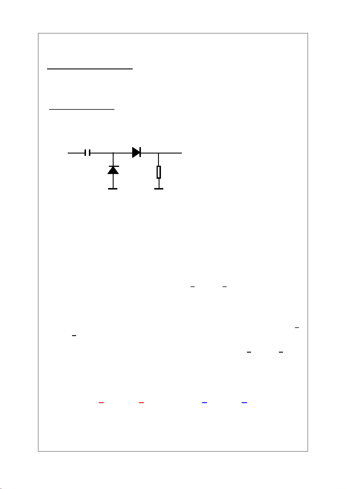
8、X rays over voltage protecting circuit test:
TV enter working mode,apply more than 27V DC voltage between two ends of
C249,the set should enter protecting mode,or check X rays protecting circuit.
4

No.:YF-Fk07-2002 ( Page 5, 9 pages in total)
9、PS line polarities test:
Connect follow the graphic below:
DC PS
9V
- +
Sound reminder
DX 2.2k
PS socket M
TO F801
Plug the PS line onto the PS socket M, then touch any pin of F801 with the
probe, the LED DX will shine at the moment, with sound reminder, or it is
disqualification.
10、PS power test:(Random test)
Instruments: Power meter.
Input signal pattern: Color bar,Sound 1KHZ ,100% modulation.
Input signal intensity: ≥60dBuv (1 mV rms)
Test points: find the graphic below
Test means: Set the Brightness, CR to the highest, adjust the volume to make
the sound output to be 0.5W. Connect the power meter to test
the power consumption. Transfer the set to be standby, and test
the power consumption at the moment, which should meet the
requirements below:
Model Power Standby power (120V)
29185N6
25185N6
114 W ± 10%
109 W ± 10%
< 1W
< 1W
5
No.:YF-Fk07-2002 ( Page 6, 9 pages in total)
11、High voltage and Ib value limit test( random test )
Instruments: High voltage meter, Ib meter.
Input signal pattern: White vertical
Input signal intensity: 60dBuv (1 mV rms)
Test means: Connect High voltage meter and Ib meter. Test voltage of different
Ib separately, It
should meet the requirements below:
Ib
Anode high voltage (kV)
25’ 29’
I
= 50µA
b
I
= 50µA & 1200µA
b
30.0 ± 1.0 30.0 ± 1.0
Diff. < 2 Diff. < 2
12、Heater voltage test ( random test )
Instruments :RMS voltage meter
Input signal pattern : Philips test graphic
Input signal intensity :1 mVrms(60dBuV)to 50 mVrms
Connect the RMS voltage meter to the 2 ends of CRT glowers,test the heater
voltage of highest CR and Brightness, It should meet:6.3±0.3Vrms
13、BTSC/SAP function test
BTSC/SAP do not need test,but BTSC/SAP decoder function should be tested
normal or not.
14、CCD and VOL-CHIP function test
VOL-CHIP and CCD function test,please find the service manual in detail.
15、Initialization
Under the factory mode,press“SURR”button,the screen displays“WAIT”,
when the screen displays “OK”, the initialization finished,
You can enter the next working procedure.
6
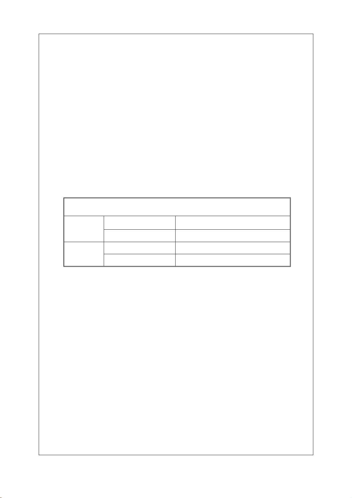
EEPROM DATA:
FAC 01 FAC 02 FAC 02 FAC 03
Item Data Item Data Item Data Item Data
RC * 80 HIGH5 1B/0D HIGH6* 1A/0E HPOS5 0C/0F
GC * 80 VP50 03/01 VP60 * 04/05 PARA5 10/11
BC * 80 VLIN5 0A/0B VLIN6* 0A/0B TRAP5 29/27
GD * 40 VSC5 0C/07 VSC6 * 0B/08 HSIZE5 1F/16
BD * 40 VBLK5 00/00 VBLK6 00/00 CNRT5 0A/08
VCEN5 32/33 VCEN6 33/35 CNRB5 06/08
VEHT5 03/03
HEHT5 03/03
FAC 03 FAC 04 FAC 05 FAC 06
Item Data Item Data Item Data Item Data
HPOS6 * 10/14 CNTX 7F BRTC 40 ST3 20
PARA6 * 0F/16 CNTN 08 COLC 2C SV3 20
TRAP6 * 27/25 BRTX 20 COLP 00 SV4 19
HSIZE6* 20/16 BRTN 20 SCOL 07 SVD 19
CNRT6 * 0B/09 COLX 35 SCNT 0C ASSH 07
CNRB6 * 07/0D COLN 00 CNTC 51/4C SHPN 10
VEHT6 03/03 TNTX 28 TNTCT 40 SHPN 2A
HEHT6 03/03 TNTN 28 TNTCV 40
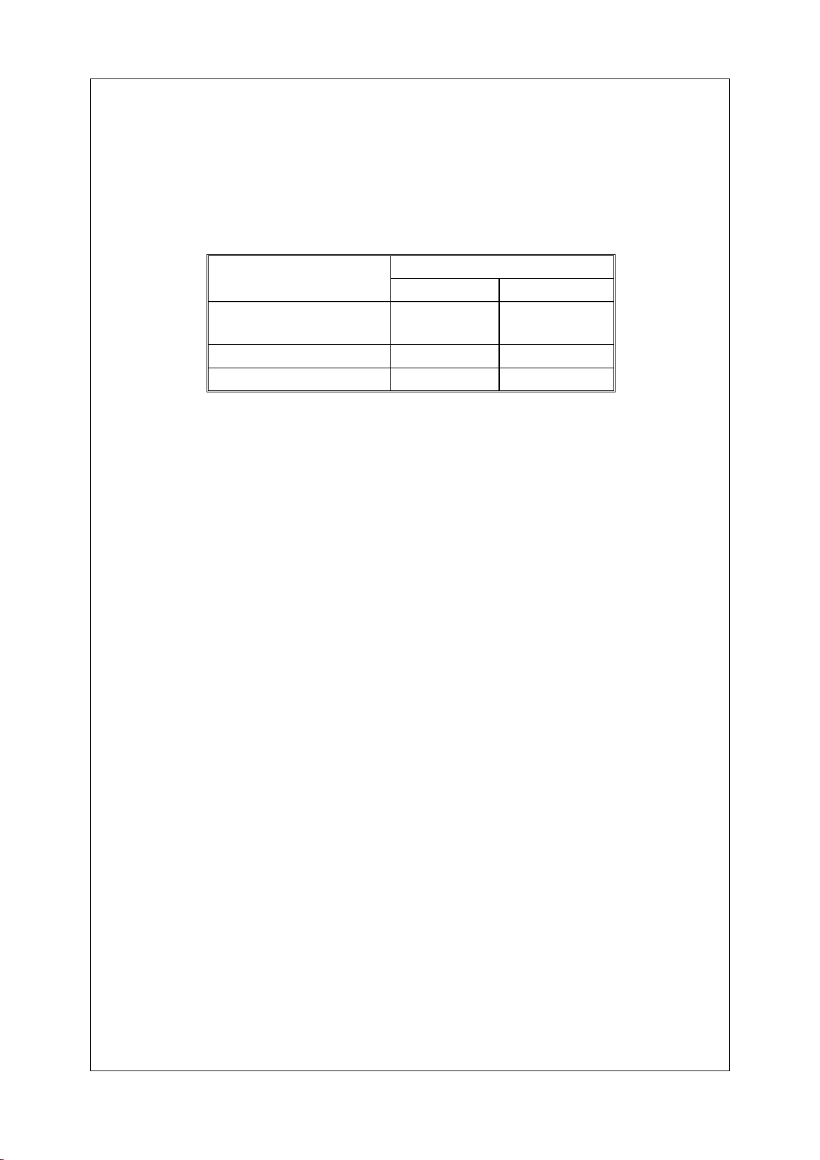
No.:YF-Fk07-2002 ( Page 7, 9 pages in total)
FAC 07 FAC 08 FAC 09 FAC 10
Item Data Item Data Item Data Item Data
MOD1 60 RFAGC * 25 V01 46 MODE4 22
MOD2 B0/30 BRTS 00 V25 6B MODE5 0B
MOD3 F0 OSD 21 V50 75 MODE6 1F
OPT 37 OSDF 53 V100 7F MODE7 C4
OPTM1 C0 CCD OSD 4A VOLMAX 32 MODE8 2D
OPTM2 C0 CCD OSDF 65 CURTCEN A5 MODE9 02/0B
HDCNT 00 TXCN 1F GATE 2A
HSTOP FF RGCN 16 VOL-OUT 73
7

No.:YF-Fk07-2002 ( Page 8, 9 pages in total)
FAC 11 FAC 12 FAC 13 FAC 14
Item Data Item Data Item Data Item Data
MPB-STR 43 SVM 05 CLTM 4B HAFC 09
MPB-HMC 0D SVM1 05 CLVO 4B AGCC 1C
MPB-HP 07 OSD2 20 CLVS 53 NOIS 01
MPB-LP 11 OSDF2 64 ABL 27 ONTM 08
MPB-LIM 00 PYNX 28 DCBS 14 NSHP 1A
SUB-FRE 28 PYNN 18 FLG0 82 PVLVL 80
SUB-HP 02 PYXS 22 FLG1 0D PLMT 80
VOL-MAI 00 PYNS 10
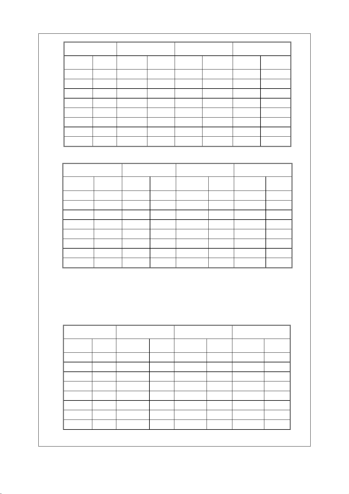
FAC 15 FAC 16 FAC 17 FAC 18
Item Data Item Data Item Data Item Data
RC-C 0 RC-W 0 D-COL 32 S-COL 32
GC-C 0 GC-W 0 D-BRI 32 S-BRI 32
BC-C 0 BC-W 0 D-CON 5A S-CON 32
GD-C 00 GD-W 00 D-SHP 32 S-SHP 32
BD-C 00 BD-W 00
YUVGC 03
YUVBC 03
FAC 19 FAC 20 FAC 21 FAC 22
Item Data Item Data Item Data Item
M-COL 32 SEG-POINT1 173 T-Hz120-BAS 5A C-Hz120-BAS 32
M-BRI 32 SEG-POINT2 407 T-Hz500-TRE 5A C-Hz500-TRE 32
M-CON 1E DATA-VL 01 T-Hz1K5 0C C-Hz1K5 0C
M-SHP 32 DATA-VH 02 T-Hz5K 0C C-Hz5K 0C
DATA-UF 08 T-Hz10K 0C C-Hz10K 0C
SPE-POS1 06
SPE-DATA1 05
SENSI-ON 00
SENSI-OFF 00
Dat
a
8

No.:YF-Fk07-2002 ( Page 9, 9 pages in total)
FAC 23 FAC 24
Item Data Item Data
B-Hz120-BAS 14 COMB1 00
B-Hz500-TRE 14 COMB2 05
B-Hz1K5 0C COMB3 00
B-Hz5K 0C AV GAIN 19
B-Hz10K 0C
Note:the items with * are adjustable, other items are not, pls do not adjust them;
9


Q
p
Fuse Blown
Is it IC801 PIN1 shorted
to earth?
Yes
Check / Replace
IC801
No raster, abnormal + B
Voltage
Is the + B, +13V, +12V, +9V
resistance to earth?
No
Check/Replace the load of the
abnormal branch
Figure 1 Fuse Blown
No
Check the components such as C801,
C802, C806, C807, C815, R801, etc.
Figure2 No Raster, Abnormal +B
Yes
Is DB801 OK?
Yes
Check IC201, IC202
and their peripheral
components
No
Yes
Check IC801 and their
eripheral components
Replace DB801
Check Q820
Q821, Q823
822,Q825etc.
Yes
Yes
Check T802 etc.

NO
No
es
Q
No raster, +B ok
Is the +9V, +5V
resistance to earth?
Check/Replace
the load of the
abnormal branch
Is both +14V and -14V ok?
Is the wave ok at Pin6 of IC301?
Check vertical scan circuit
Figure3 No Raster, +B OK
Is there a output
Y
waveform Pin13
of IC101?
Is Pin2 of IC101 low
voltage level?
Is B of Q202 low
voltage level?
Yes
Yes
No
No
Yes
No
Y
No
Check horizontal scan circuit, such
as C412, C413, C419, etc
Is there the wave
at C of
Check\replace
the drive circuit
411?
Is the drive
circuit ok?
No
Yes
Replace FBT
Is R461
ok?
Increase
VG2
Yes
Yes
NG
No
Replace
R461

es No
No
es
C10
No picture, dense noise
dots
Is the antenna feed line
or the adapter broken
or unsoldered?
Y
Handing the antenna
fault
Figure 4 No Picture dense noise dots
Is the signal at
Pin41, Pin42 of
IC101 ok?
No
Is the signal at IF
pin of the tuner ok?
Is the signal at Pin SCL,
SDA of tuner ok?
No
Check signal at P5, P57, P58, P59,
and P60 of IC101 and replace the
abnormal relative circuit
Yes
Check EEPROM
Y
Yes
Yes
Check/Replace
1
I
Check the relative
circuit of Q101,
Z141 etc
Is the supply voltage
of tuner ok?
No
Check/Replace
IC201, IC202, D101.
Yes
Check/Replace
Tuner

g
y
g
Symptom: raster ok, no
picture, no sound, sparse
noise dots
Apply the pointer of
multimeter at R X 1 KΩ,
connect one probe to GND,
use another to touch Pin42 of
IC101. Are there interference
particles flashin
screen?
on the
No
Yes
Unsolder a pin of C107, apply the
pointer of multimeter at R X 1 K
Ω, connect the red probe to GND,
use the black probe to touch B of
Q101. Are there interference
particles flashing on the screen?
Yes
Replace the Tuner
Figure 5 Sparse noise dots
Is the voltage
at Pin29, P36
of IC101 ok?
Bridge a capacitor of 1000pF between
the input and output of Z141. Appl
the pointer of multimeter at R X 1 KΩ,
connect the red probe to GND, and use
No
the black probe to touch B of Q101 Are
there interference particles flashin
the screen
Replace Z141 (SAW)
No
Yes
Check and repair
the +9V power
supply
on
No
Yes
Does the IF
pre-amplifier
work
normally?
No
Check &
repair the IF
pre-amplifier

y
y
No sound
Is the speaker ok?
No
Replace the speaker
Yes
Apply the pointer of multimeter at
RX1KΩ connect one probe to GND,
use another to touch Pin4, Pin12 of
IC602, Is there interference noise
from the speaker.
Yes
Is the waveform
at Pin47 of
IC1001 ok?
Check/Replace the power
Yes
of IC1001. Then
suppl
RESET
No
Check/Replace
Q203, X202 etc.
NG
Figure 6 No Sound
No
Is the waveform at
Pin30 of IC101 ok?
Check power
of IC602
suppl
NG
Yes
Is the BUS
ok?
No
Replace IC101
Is it mute at P6
of IC602?
No
Check IC101 and
the relative circuit
No
Yes
Replace
IC602
Check/Replace
Q601, Q602
and Q603 etc.

yway
No Picture
Figure 7 no Picture
TV&AV
haven’t
Picture
TV has
Picture. AV
hasn’t
Picture.
AV has
Picture. TV
hasn’t
Picture.
Ok
Is RGB signal
ok?
Is the waveform at
Pin12, Pin14 of
IC901 ok?
Check Q901 ~
Q904 alle
circuit
Is the waveform
at P15 of IC901
ok?
Is +9V,
+200V ok?
No
No
No
Check Q203, Q204
and alleyway circuit
Is the waveform at
P30 of IC101 ok?
Check Pin20,
Pin24 of IC101
No
Yes
Yes
Yes
Check
Yes Yes
Q501~Q506
Yes
Check P13 of IC901
Is the logic at P9,
P10 of IC901 ok?
Yes
Replace IC901
Is the logic at
P9, P10 of
IC901 ok?
No
No
Yes
Check IC101 and
relative circ uit. plea se
reference the previous
page named Figure 5.
Check R516 ~ R521
etc.
Check P25, P49
of IC101 and the
relative circuit
Check Q917 and
NG
Video alleyway Circuit
Check P1 of IC101,
P4 of IC1001 and
the relative circuit
Replace
IC901
Check P1 of IC101, P4 of
No
IC1001 and the relative
circuit
NG
Replace
IC101

,
,
Figure 8 No Vertical Scanning
Yes
Is both +14V and -14V ok?
No
Yes
Is the signal at P1 of IC301
ok?
No
Check/Replace R431,
D431, D432 etc
R433
Check/Replace IC301
No
Check signal at P16 of
IC101
Yes
Check/Replace IC101
Check/Replace R245,
R313.
R311

g
k
y
y
g
f
y
Symptom:
Control
Tunin
not wor
Press
STANBY ke
on R/C. Can
the TV be
turn on and
turn off?
No
①
Yes
Does the channel
number displa
on the screen?
No
Yes
Start au to search. Is
the BUS ok?
No
Yes
After auto-search, Can
the searched pro
memorized?
ram be
Check the
waveform
at Pin60,
Pin61 of
IC101
Is there sync
No
pulse at P62 of
IC101?
Check the power
supply of IC101.
Are there H & V
back pulses at
fl
Pin12 of IC101
Yes
Check/Replace
IC101
No
Is the
Yes
+33V/+5V
A power
supply
ok?
No
Is there sync
pulse at B of
Q003?
Yes
Replace Q003
No
No
Check R314, R315,
R316, C311, D303
Check/Repair +33V
power supply
Is there the
short circuit
Yes
Check Q915, Q916
and the relative
circuit.
around the
integration
circuit?
Is the voltage at
IC001ok?
P8 o
No
Check/Repair +5V
power supply.
No
No
Yes
Replace IC001
Yes
Figure 9
Check/Replace
the tuner
Check/Repair the
integration circuit

g
①
Figure 10 Tuning Control no working
Is there any change on
the volta
of IC101?
e level at P64
No
Check the remote control
receiver and transmitter.
Yes
Is the VDD(+5V) at P9
and P55 of IC101 ok?
Yes
Is there the 8MHz/5Vp-p
sine wave oscillations at P6
of IC101?
Yes
No
Is the voltage at P5 of
IC101 ok?
Yes
Have P5 of IC101 shorted to
GND in an instant. Can the
IC101 work?
Yes
Check/Repair the reset
circuit.
No
Check
Q007 etc.
No
Are C031, C032
and X001 ok?
Replace the disabled
components
No
Check/Replace
IC101
Yes
No

 Loading...