

Page 1

LP-10T
SERVICE MANUAL
Page 2

1.0 Introduction
1.1 Operation Specification
1.2 Functional Specification
1.3 Control And Adjustment
2.0 Theory Of Operation
2.1 Main Board
2.2 Keypad Board:
2.3 Inverter Board:
CONTENTS
3.0 Troubleshooting Instruction
3.1 No Display, Power Indicator Is Off Or Blinking
3.2 No Display, Power Indicator Is Orange
3.3 No Display, Power Indicator Is Green
4.0 Video Connector Pin Assignment
5.0 Visual Inspection Criteria-LCD Panel
5.1 Criteria (acceptable)
5.2 External inspection
6.0 Spare Parts List
Page 3

7.0 Circuit Diagram
7.1 Power Distribution
7.2 VGA Input
7.3 ADC
7.4 Damping Network
7.5 Frame Rate Conversion
7.6 ASI 321
7.7 ASI 321 Power & EXT. OSD
7.8 Micro controller
7.9 Panel Interface
8.0 Layout Diagram
(To be confirmed)
9.0 Parts List
Page 4

Audience
This service manual is primarily for system engineers, service engineers, dealers and
distributors. It carries the assumption that reader understands the basic operating concepts.
Purpose
This manual contains reference data for LP-10T21 LCD monitor. It gives information
regarding the operating principles of monitors, as well as technical service and maintenance
information.
1.0 Introduction
About This Manual
The LP-10T is a high performance 10.4” TFT LCD monitor. This micro-controlled monitor is
designed for continuous operation from 31.5 to 48 KHz and is capable of displaying up to a
resolution of 800 *600 in interface mode. The razor sharp flicker-free image, and the
delicate ergonomic design of this monitor elevate not only productivity but also the user’s
comfort.
1.1 Operation Specification
1.1.1 Operation Environment
Temperature
Operation:0 to 40℃
Storage:-20 to 60℃
Humidity (Relative)
Operation:10 to 80% non-condensing
Storage:10 to 90% non-condensing
Altitude
Operation:0~8000ft
Storage:0~40000ft
Page 5

1.1.2 Safety, Ergonomic, EMC Compliance
This monitor complies with the following safety, ergonomic, and EMC standard
UL:UL1950, Third Edition
FCC:FCC Rules and CISPR22 (Docket NO. 92-152, SEP. 1993) and FCC/
ANSIC63.K-1992
TUV-GS:EN60950→ 1992+A1+A2+A3+A4+A11 and EK1-ITB2000
CUL:CAN / CSA C22.2 NO.950
CE(EMC):EN55022/1998 and EN61000-3-2 / 1995 +A12/1996 +A13 / 1997
+A1/1998 +A2/1998 and EN61000-3-3/1995 and EN5502K / 1998
CE(LVD):EN60950→ 1992+A1+A2+A3+A4+A11
1.1.3 Signal Input Requirement
Connector:
15 pin D-Sub high-density connector for video and sync signals. See chapter 4 for
pin assignment.
Video Signals:
Type: Red, Green, Blue channels analog input.
Level: 0.7Vp-p
Impedance:75 ohms.
Sync Signals:
Type: Separate Horizontal and Vertical Sync
Level: TTL Level
Polarity: Positive or negative
1.1.4 Power Input Requirement
Operating voltage range
100~240 V AC at 50/60 Hz
Power Consumption
Normal Operation: 19W
Stand by: 2.5W
Suspend mode: 2.5W
Off mode: 2.5W
Page 6
1.2 Functional Specification
The standard conditions for verifying the following specification are:
Temperature: 25±5℃
Warm-Up Time: 15 minutes minimum
AC line input: 100~240 V AC±10%, 50 / 60±3Hz
View Distance: 30cm
1.2.1 Display Quality
Display Size (H*Z): 211.2mm*158.4mm
Brightness: more than 120 cd/ m
2
Contrast Ratio: 180:1
1.2.2 Color Quality
White Balance (Use full white pattern, set brightness to maximum)
At color temperature of white light CIE9300
o
K+27M..P.C.D
X=0.283±0.02, Y=0.298±0.02
At color temperature of white light CIE6500
X=0.313±0.02, Y=0.329±0.02
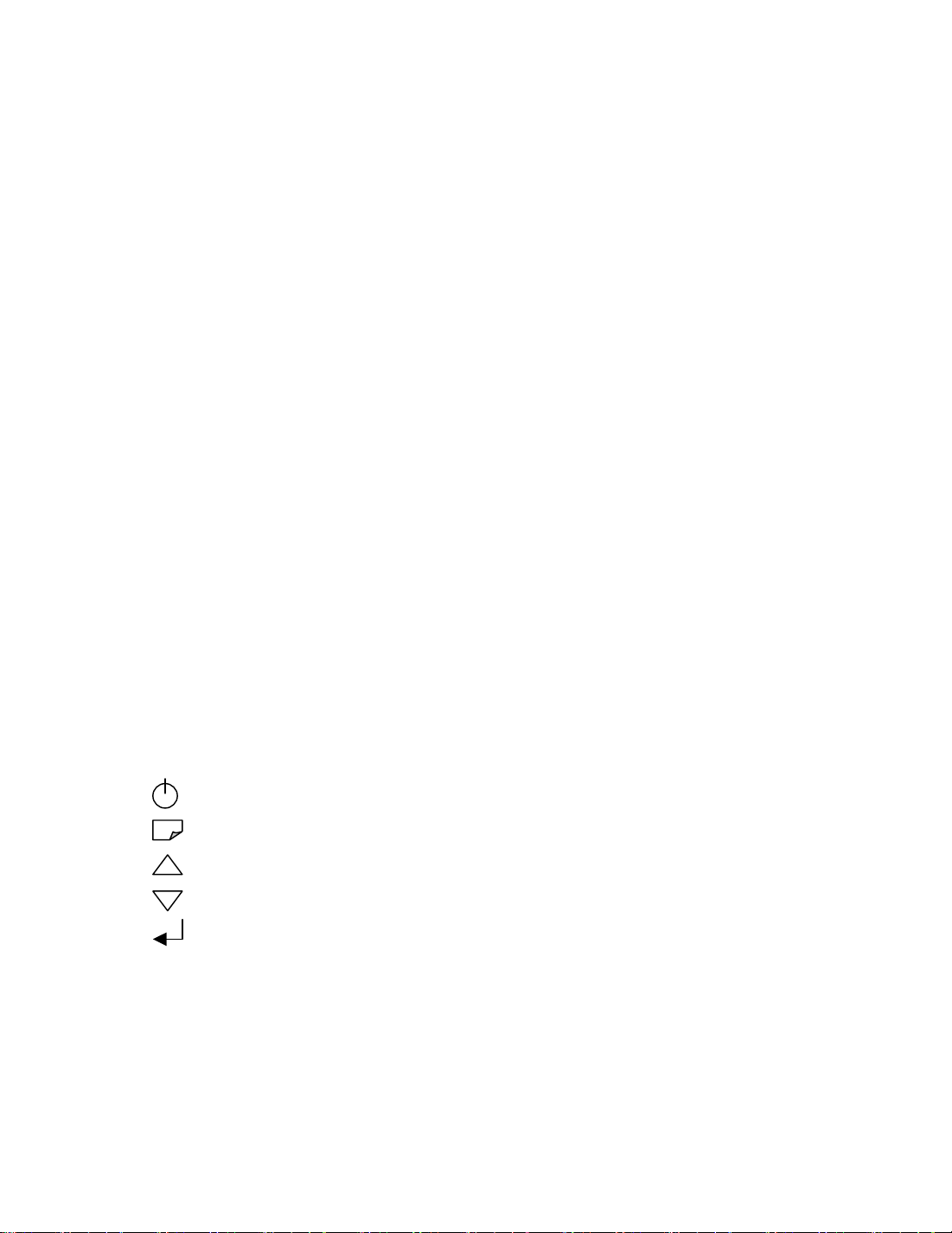
1.3 Control And Adjustment
1.3.1 External User Controls
POWER Power On / Off
MENU OSD Menu On / Off
UP Increase the Value.
DOWN Decrease the Value.
ENTER Confirm the selection
1.3.2 Controlled Functions From OSD Menu
Brightness: Press (+) key to increase brightness, (-) key to decrease brightness.
Contrast: Press (+) key to increase contrast, (-) key to decrease contrast.
o
K+27M..P.C.D
Auto Adjust: Press (+) or (-) to adjust H-phase & H-position & V-position clock
automatically.
Page 7

Phase: By varying this (+)(-) control the exact sampling time within the pixel can
be adjusted.
Clock: Adjust sampling clock of analog to digital converter until clock is equal to
pixel frequency of video input.
H-Position: Press (+) key to shift screen right, (-) key to shift screen left.
V-Position: Press (+) key to shift picture upward, (-) key to shift picture downward.
Sharpness: Press (+) key to increase sharpness, (-) key to decrease Sharpness.
Color Temp: Press (+) or (-) to choose three types of color temperature 9300,
6500 and user define.
Language: Press (+) or (-) to choose any one of the following languages: English,
French, German, Italian and Spanish.
OSD: Adjust OSD frame location, timeout, transparency and preset OSD.
Dos-text / graphic: Select display quality (text / graphic) when this monitor is used
in DOS.
Recall: Recall the default value.
1.3.3 Special Functions
Automatic storing: After adjusting the screen parameters, the microprocessor
automatically stores the screen settings in user mode.
Entering factory mode: Press (+) and (-) at same moment before power on, the
monitor will operate in factory mode. In this mode, the value of brightness, contrast,
black-level, red, green, phase, OSD time, color save (color temperature) is stored
as default value. During recall function, these values will be recalled again.
2.0 Theory Of Operation
2.1 Main Board
This module consists of microprocessor, Cheetah chip, AD converter, memory, clock
generator, power conversion, 3.3-volt regulator and backlight controller.
Page 8

2.1.1 A/D (AD9884A U8):
U8 is a triple 8-bit ADC with controllable amplifiers and clamps for the digitizing of
large bandwidth RGB signals. The clamp level, the gain and all of the other
settings are controlled via a serial interface, SDA (pin29), SCL (pin30).
Analog video inputs (Rin, Gin, Bin) are internal DC polarized. These inputs are AC
coupled by C46, C52, and C54 - three capacitors. ADC outputs R0~R7, G0~G7,
B0~B7 are connected to scaling IC (ASI-320) via resistor array.
2.1.2 Scaling IC (ASI-320 U14):
U14 provides memory interface, ADC interface, microprocessor interface and flat
panel interface. U14 can work either with or without the external frame buffer. The
scaling IC is the data follow center between SDRAM (U12, U13), A/D converter
(U8), MCU (U17) and LVDS transmitter (U20). Because the LVDS panel is 6
bits/color system, scaling IC also dither the 8 bits/color (from A/D) to 6bits/color
system
2.1.3 Memory:
U12~U13 (A43L0616V-7) for 1M*16 SDRAM frame buffer. 2.1.4 Power conversion:
U1: Main 5 volts output are generated by DC to DC conversion, from adapter we
get 12 volts DC input, convert 12 volts to 5 volts.
2.1.4 Regulator
3.3 volts regulator: U2, U4, U5, U6 are 3.3 volt regulators.
U2 output for LCD panel
U4 output for scaling IC (U14) and AD9884 (U8).
U5 output for SDRAM (U12, U13) and LVDS transmitter (U20)
U5 output for analog power of AD9884 (U8)
2.1.5 LVDS transmitter (U20)
U20 transmits the LVTTL color data via LVDS interface.
2.1.6 MCU (U17)
Dominate the OSD, preset mode, factory initial mode etc.
Page 9

2.2 Keypad Board:
The key status input to Main Board for function adjustments ON OSD menu.
2.3 Inverter Board:
Inverts DC to high voltage AC for driving CCFL.
3.0 Troubleshooting Instruction
3.1 No Display, Power Indicator Is Off Or Blinking
3.1.1 Check AC/DC adaptor is proper installed with power code or DC jack.
3.1.2 Make sure having pressed power key.
3.2 No Display, Power Indicator Is Orange
3.2.1 Check the connector VGA1 for RGB signals input to Main board or not.
3.2.2 Change the Main Board
3.3 No Display, Power Indicator Is Green
3.3.1 Check the connector P7 for LVDS signals input to panel or not.
3.3.2 Check the LCD panel connector.
3.3.3 Check CON4 for power input of inverter.
3.3.4 Change the inverter board
3.3.5 Change the Main board
Page 10

4.0 Video Connector Pin Assignment
Pin NO. Signal Pin NO. Signal
1 R Signal 9 -----------2 G Signal 10 Sync Ground
3 B Signal 11 -----------4 ------------ 12 DDC Serial Data Line
5 Ground 13 Horizontal Sync
6 R Ground 14 Vertical Sync
7 G Ground 15 DDC Data Clock Line
8 B Ground
5.0 Visual Inspection Criteria-LCD Panel
5.1 Criteria (acceptable)
Random R, G or B 1 dot N≦ 3
Adjacent 2 dots ≦ 1 Pairs
Bright Dot
Adjacent 3 or more dots 0 Pairs
Minimum distance between bright dots 15mm
Random R, G or B 1 dot N≦ 4
Adjacent 2 dots ≦ 1 Pairs
Dark Dot
Adjacent 3 or more dots 0 Pairs
Minimum distance between bright dots 5mm
Total bright and dark dots N≦ 7
(1) Dot smaller than half dot is not counted as a defective dot.
(2) The adjacent dots defect is defined as align vertical, horizontal and diagonal
direction.
(3) The detailed dot defect diagrams are showed as below.
Item Accept Count
Page 11

5.2 External inspection
Extraneous Substances
Polarizer Scratches 0.05≦ W≦ 0.1, L≦ 1.5, N≦ 3
Polarizer Dent / Bubble 0.1≦ D≦ 0.5, N≦ 3
Width: W (mm), Length: L (mm), Average diameter: D (mm)
Average Diameter: D
D=(a+b)/2
a(L)
6.0 Spare Parts List
Items To Be Inspected
Inspection Standards
(Acceptable Level))
Circular 0.1≦ D≦ 0.5, N≦ 3
Liner 0.05≦ W≦ 0.1, L≦ 1.5, N≦ 3
b(W)
Parts No. Description Notes
1 Main Board 891-0100-068
2 Transfer Board 891-0310-002
3 Inverter 891-0250-003
4 Keypad 891-0010-010
5 Driving Board 891-0280-001
6 Power Adaptor 560-1000-002
7 LCD Panel 501-1044-321
Page 12

7.0 Circuit Diagram
7.1 Power Distribution
CON1
DC JACK2.5
+12V
+12V +12INV
VCC5
P.10
INV_ON/OFF
P.10
PANEL_ON/OFF
F1
QT3216KL100HC-3A
R251003
QT4532KL150HC-3A
C19
C17
+
104
470u/25V
QT3225KL060MC-1.5A
C27
104
INV_ON/OFF
PANEL_ON/OFF
L40
L6
L4
QT4532KL150HC-3A
C3
C1
+
104
470u/16V
GND_POWER
C20
104
C28
C26
+
104
470u/16V
L1
C18
+
470u/16V
DVCC5
QT3225KL060MC-1.5A
L7
QT3225KL060MC-1.5A
L9
C4
C2
+
104
470u/16V
C15 103 R59 15K
R53
10K
C9
104
C16 220pF
C262
104
C263
10uF/25V
6
3
1
5
Inverter
Power
MCU, ROM & Glue
Logics
H2,AD9884,LVDS
,SDRAM,PANEL
U4
VOUTVIN
U6
VSS
RC1587M
1
C264
NC
VOUTVIN
VSS
AS1117M/3.3V
1
C32
104
C40
104
ENABLE
SS
RT
FB
23
100R,(0805,1%)
23
U1
14
111213
NCNCNC
VCC
COMP
GND
4
7
R223
R224
169R,(0805,1%)
AVCC3
C41
104
D1
1N4148
2
OCSET
10
BOOT
9
UGATE
8
PHASE
HIP6013
DVCC3
C33
C31
+
104
470u/16V
Analog Power
C39
+
to ADC
470u/16V
C5 102
R56 10K
DVCC5
Q2
R2030
RFD3055SM
VCC
PANEL_ON/OFF
ZD1
MBR340T3
DVCC5
14
1 2
7
DVCC5
INV_ON/OFF
C10
104
70uH/COIL/3A
U3A
74HCT14
GND
L3
R63
4.7K
R67 10K
R61
10K
R62 2.7K
C8
104
PVCC_5/3V
R64
1K
C6
+
470u/16V
C29
104
R65
1K
R66 NC
Q5
3904
C7
+
470u/16V
R60
51K
Q4
3904
R54
30K
R58
10K
Q3
1
S
2
S
3
S
4 5
GD
9435A
BGT_ADJ
R68
0
VCC5
R55
30K(NC)
8
D
7
D
6
D
CON4
1
2
3
4
5
WAFER,2022-05/DIP
DVCC3
C23
104
VCC5
DVCC5
DVCC3
AVCC3
PVCC+12INV
GND_POWER
PANEL3.3V
QT3225KL060MC-1.5A
L2
QT3225KL060MC-1.5A
C21
L5
+
47uF/10V,LESR
VCC5
DVCC5
DVCC3
AVCC3
PVCC
GND_POWER
PVCC_5/3V
C12
C14
+
470u/10V
104
PVCC
C22
C24
+
47uF/10V,LESR
104
P.02,03,09,10
P.03,04,05,09,10,11
P.02,03,05,09
P.11
APPROVED
DRAWING
Size Document Number Rev
B
Date: Sheet
0LP-10T21 Power Distribution
of
19Friday, January 05, 2001
Page 13

7.2 VGA Input
VGA1
1
6
11
2
7
12
3
8
13
4
9
14
5
10
15
CON VGA DB15
TCH1
1
2
3
4
CON4/2.0
P. 01
P. 01
VGA_R
VGA_R_GND
VGA_G
VGA_G_GND
DDC_SDA
VGA_B
VGA_B_GND
VGA_HSYNC
VGA_CVCC5
VGA_VSYNC
DDC_SCL
DVCC5
XH
YH
XL
YL
DVCC5
AVCC3
JY-5017-06
DIN 1
8
2
VCC
R69 NC
AVCC3
L10 BEAD
L11 BEAD D2
L12 BEAD
D3
CVCC5
1N4148
D5
D4
D9
5.6VD85.6V
365
1
DVCC5
AVCC3
C47
5.6V
100pF
C48
5.6V
100pF
3
12
1 2
DAN217-T146(ROHM)
AVCC3
D6
3
12
1 2
DAN217-T146
AVCC3
D10
3
12
1 2
DAN217-T146
C46 47nF
3
3
3
R74
75
C52 47nF
R80
75
R82
75
R73 270
R79 270
R81 270C54 47nF
RED
GREEN
BLUE
R70 0
R76 0
CVCC5
1
2
3
4 5
U7
NC
NC
NC
VSS SDA
24LC21
U3B
3 4 R71 0
C43
74HCT14
NC
U3D
9 8
C49
74HCT14
NC
C53
104
8
VCC
7
VCLK
6
SCL
R75 NC
R204
10K(NC)
R207 47
R208 47
R209 47
RED
GREEN
BLUE
HSYNC
VSYNC
GND_POWER
DVCC5
14
U3C
5 6
C44
7
74HCT14
NC
U3E
11 10R77 0 R78 33
C50
74HCT14
NC
R205
R206
10K
10K
VGA_VSYNC
DDC_SCL
DDC_SDA
RED
GREEN
BLUE
HSYNC
VSYNC
GND_POWER
GND
D7
1N4148
P. 03
P. 03
P. 03
P. 03,08
P. 03,08
R72 33
DVCC5
C42
104
HSYNCVGA_HSYNC
C45
NC
VSYNCVGA_VSYNC
C51
NC
GND_POWER
APPROVED
DRAWING
Size Document Number Rev
B
LP-10T21 VGA Input
Date: Sheet
0
of
29Friday, January 05, 2001
Page 14

DVCC3
DVCC3
P.01
P.01
P.01
P.02
P.02
P.02
P.02
P.02
P.08
P.08
P.08
P.08
P.08
D13 1N4148(NC)
HSYNC
HSTOPLL
D14 1N4148(NC)
VSYNC
DVCC5
DVCC3
AVCC3
VSYNC
HSYNC
RED
GREEN
BLUE
SCL
SDA
HSTOPLL
CLAMP
PIO6
R83 10K(NC)
R84 1K(NC)
R85 33
R86 NC
R89 NC
VCC
DVCC5
DVCC3
AVCC3
VSYNC
HSYNC
RED
GREEN
BLUE
SCL
SDA
HSTOPLL
CLAMP
PIO6
C55
47uF/10V,LESR
47uF/10V,LESR
R92
0
L13
QT2012
C56
+
104
47uF/10V,LESR
C0603
L14
QT2012
C71
+
C70
104
C0603
R87
CLAMP
NC
Serial Port Address Select
for AD9884A
DVCC3
R99
NC
AD_A0 AD_A1 CKINV
R103
0
102
128
1
DVCC3_ADDVCC3
C58
+
C57
104
C0603
+
C72
47uF/10V,LESR
AVCC3 PVD
+
C82
47uF/10V,LESR
GREEN
R88 NC
R90
1K
Sampling Clock Inversion
Tie high to invert.
Tie low for normal rising
edge.
DVCC3
R100
NC
R104
0
64
38
AVCC3_ADAVCC3
C73
104
C0603
C83
104
C0603
C59
104
C0603
L15
QT2012
47uF/10V,LESR
R91
0
R101
NC
R105
0
GND_POWER
C60
104
C0603
C74
104
C0603
U8
4
VD
8
VD
10
C67
C66
C65
C64
C63
C62
C61
104
C0603
C75
104
C0603
+
C84
R93
10K
104
C0603
C76
104
C0603
C85
104
C0603
CKINV
SDA
SCL
AD_A0
AD_A1
PIO6
104
C0603
C77
104
C0603
R94 150
R95 150
DVCC5
14
1 2
7
GCLOCK
HSFRMPLL
CSYNC
ADREVEN[0..7]
ADGEVEN[0..7]
ADBEVEN[0..7]
ADRODD[0..7]
ADGODD[0..7]
ADBODD[0..7]
GND_POWER
104
C0603
C78
104
C0603
C86
104
C0603
U9A
74HCT14
104
104
C0603
C0603
C80
C79
104
104
C0603
C0603
C88
C87
104
104
C0603
C0603
DVCC3
GND
GCLOCK
HSFRMPLL
CSYNC
ADREVEN[0..7]
ADGEVEN[0..7]
ADBEVEN[0..7]
ADRODD[0..7]
ADGODD[0..7]
ADBODD[0..7]
GND_POWER
104
C0603
C81
104
C0603
C89
104
C0603
R96
NC
P.08
P.08
P.08
P.06
P.06
P.06
P.06
P.06
P.06
RED
GREEN
BLUE
11
16
18
19
23
25
124
128
54
64
74
84
94
104
114
120
33
34
43
48
50
7
15
22
40
41
28
14
44
27
29
30
31
32
125
5
6
9
12
13
17
20
21
24
26
35
39
42
47
49
51
52
53
63
73
83
93
103
113
119
121
122
123
VD
VD
VD
VD
VD
VD
VD
VD
VD
VDD
VDD
VDD
VDD
VDD
VDD
VDD
VDD
PVD
PVD
PVD
PVD
PVD
RAIN
GAIN
BAIN
HSYNC
COAST
CLAMP
SOGIN
CKEXT
CKINV
SDA
SCL
A0
A1
PWRDN
GND
GND
GND
GND
GND
GND
GND
GND
GND
GND
GND
GND
GND
GND
GND
GND
GND
GND
GND
GND
GND
GND
GND
GND
GND
GND
GND
GND
AD9884
APPROVED
112
DRA0
111
DRA1
110
DRA2
109
DRA3
108
DRA4
107
DRA5
106
DRA6
105
DRA7
92
DGA0
91
DGA1
90
DGA2
89
DGA3
88
DGA4
87
DGA5
86
DGA6
85
DGA7
72
DBA0
71
DBA1
70
DBA2
69
DBA3
68
DBA4
67
DBA5
66
DBA6
65
DBA7
102
DRB0
101
DRB1
100
DRB2
099
DRB3
098
DRB4
097
DRB5
096
DRB6
095
DRB7
82
DGB0
81
DGB1
80
DGB2
79
DGB3
78
DGB4
77
DGB5
76
DGB6
75
DGB7
62
DBB0
61
DBB1
60
DBB2
59
DBB3
58
DBB4
57
DBB5
56
DBB6
55
DBB7
118
SOGOUT
117
HSOUT
45
FILT
127
REFIN
126
REFOUT
1
NC
2
NC
3
NC
36
NC
37
NC
38
NC
46
NC
115
DATACK
116
/DATACK
DRAWING
ADREVEN0
ADREVEN1
ADREVEN2
ADREVEN3
ADREVEN4
ADREVEN5
ADREVEN6
ADREVEN7
ADGEVEN0
ADGEVEN1
ADGEVEN2
ADGEVEN3
ADGEVEN4
ADGEVEN5
ADGEVEN6
ADGEVEN7
ADBEVEN0
ADBEVEN1
ADBEVEN2
ADBEVEN3
ADBEVEN4
ADBEVEN5
ADBEVEN6
ADBEVEN7
ADRODD0
ADRODD1
ADRODD2
ADRODD3
ADRODD4
ADRODD5
ADRODD6
ADRODD7
ADGODD0
ADGODD1
ADGODD2
ADGODD3
ADGODD4
ADGODD5
ADGODD6
ADGODD7
ADBODD0
ADBODD1
ADBODD2
ADBODD3
ADBODD4
ADBODD5
ADBODD6
ADBODD7
Size Document Number Rev
B
Date: Sheet
393,5%,NPO
C95
104
3.3K,1%
R106 33
R107 NC
LP-10T21 ADC
ADREVEN[0..7]
ADGEVEN[0..7]
ADBEVEN[0..7]
ADRODD[0..7]
ADGODD[0..7]
ADBODD[0..7]
R97 NC
R98 0
C91
392,5%,NPO
R102
CSYNC
HSFRMPLL
C92
L39
QT2012
Reserved
C93
+
47uF/10V,LESR
C94
10pF
39Friday, January 05, 2001
C96
104
GCLOCK
of
PVD
0
Page 15

7.4 Damping Network
P.03
P.03
P.03
P.03
P.03
P.03
ADREVEN[0..7]
ADGEVEN[0..7]
ADBEVEN[0..7]
ADRODD[0..7]
ADGODD[0..7]
ADBODD[0..7]
ADREVEN[0..7]
ADGEVEN[0..7]
ADBEVEN[0..7]
ADRODD[0..7]
ADGODD[0..7]
ADBODD[0..7]
ADREVEN[0..7]
ADGEVEN[0..7]
ADBEVEN[0..7]
ADRODD[0..7]
ADGODD[0..7]
ADBODD[0..7]
Analog Interface
Damping Network
RA1
1 8
ADREVEN0
2 7
ADREVEN1
3 6
ADREVEN2
4 5
ADREVEN3
ADREVEN4
ADREVEN5
ADREVEN6
ADREVEN7
ADGEVEN0
ADGEVEN1
ADGEVEN2
ADGEVEN3
ADGEVEN4
ADGEVEN5
ADGEVEN6
ADGEVEN7
ADBEVEN0
ADBEVEN1
ADBEVEN2
ADBEVEN3
ADBEVEN4
ADBEVEN5
ADBEVEN6
ADBEVEN7
ADRODD0
ADRODD1
ADRODD2
ADRODD3
ADRODD4
ADRODD5
ADRODD6
ADRODD7
ADGODD0
ADGODD1
ADGODD2
ADGODD3
ADGODD4
ADGODD5
ADGODD6
ADGODD7
ADBODD0
ADBODD1
ADBODD2
ADBODD3
ADBODD4
ADBODD5
ADBODD6
ADBODD7
R-PACK4 33
RA3
1 8
2 7
3 6
4 5
R-PACK4 33
RA5
1 8
2 7
3 6
4 5
R-PACK4 33
RA7
1 8
2 7
3 6
4 5
R-PACK4 33
RA10
1 8
2 7
3 6
4 5
R-PACK4 33
RA12
1 8
2 7
3 6
4 5
R-PACK4 33
RA13
1 8
2 7
3 6
4 5
R-PACK4 33
RA15
1 8
2 7
3 6
4 5
R-PACK4 33
RA17
1 8
2 7
3 6
4 5
R-PACK4 33
RA19
1 8
2 7
3 6
4 5
R-PACK4 33
RA21
1 8
2 7
3 6
4 5
R-PACK4 33
RA23
1 8
2 7
3 6
4 5
R-PACK4 33
HREVEN0
HREVEN1
HREVEN2
HREVEN3
HREVEN4
HREVEN5
HREVEN6
HREVEN7
HGEVEN0
HGEVEN1
HGEVEN2
HGEVEN3
HGEVEN4
HGEVEN5
HGEVEN6
HGEVEN7
HBEVEN0
HBEVEN1
HBEVEN2
HBEVEN3
HBEVEN4
HBEVEN5
HBEVEN6
HBEVEN7
HRODD0
HRODD1
HRODD2
HRODD3
HRODD4
HRODD5
HRODD6
HRODD7
HGODD0
HGODD1
HGODD2
HGODD3
HGODD4
HGODD5
HGODD6
HGODD7
HBODD0
HBODD1
HBODD2
HBODD3
HBODD4
HBODD5
HBODD6
HBODD7
HREVEN[0..7]
HGEVEN[0..7]
HBEVEN[0..7]
HRODD[0..7]
HGODD[0..7]
HBODD[0..7]
APPROVED
HREVEN[0..7]
HGEVEN[0..7]
HBEVEN[0..7]
HRODD[0..7]
HGODD[0..7]
HBODD[0..7]
P.08
P.08
P.08
P.08
P.08
P.08
DRAWING
Size Document Number Rev
Date: Sheet
Custom
LP-10T21 Damping Network
49Friday, January 05, 2001
0
of
Page 16

7.5 Frame Rate Conversion
P.01
P.08
P.08
P.08
P.08
P.08
P.08
P.08
P.08
P.08
P.08
P.08
P.08
P.08
GND_POWER
DVCC3
ADQ[0..31]
AMA[0..10]
SDCLK
SDCLKI
ACKE
/ACS
/AWE
/ACAS
/ARAS
ABA
ADQM1
ADQM0
ACBS
DVCC3
ADQ[0..31]
AMA[0..10]
R156 33
SDCLKI
GND_POWER
ACKE
/ACS
/AWE
/ACAS
/ARAS
ABA
ADQM1
ADQM0
ACBS
R154
220
R157
330
ADQ[0..31]
AMA[0..10]
R147
1 8
ADQ31
2 7
ADQ15
3 6
ADQ30
4 5
ADQ14
ADQ29
ADQ13
ADQ28
ADQ12
ADQ27
ADQ11
ADQ26
ADQ10
ADQ25
ADQ9
ADQ24
ADQ8
ADQ23
ADQ7
ADQ22
ADQ6
ADQ21
ADQ5
ADQ20
ADQ4
ADQ19
ADQ3
ADQ18
ADQ2
RA-560
R148
1 8
2 7
3 6
4 5
RA-560
R149
1 8
2 7
3 6
4 5
RA-560
R150
1 8
2 7
3 6
4 5
RA-560
R151
1 8
2 7
3 6
4 5
RA-560
R152
1 8
2 7
3 6
4 5
RA-560
R153
1 8
2 7
3 6
4 5
RA-560
R155
1 8
ADQ17
2 7
ADQ1
3 6
ADQ16
4 5
ADQ0
RA-560
R158
1 8
ACKE
2 7
/AWE
3 6
/ACS
4 5
ACBS
RA-560
R159
1 8
ADQM0
2 7
ADQM1
3 6
/ACAS /CAS
4 5
/ARAS
RA-560
R160
1 8
ABA
2 7
AMA10
3 6
AMA0
4 5
AMA1
RA-560
R161
1 8
AMA2
2 7
AMA3
3 6
AMA4
4 5
AMA5
RA-560
R162
1 8
AMA6
2 7
AMA7
3 6
AMA8
4 5
AMA9
RA-560
DQ19
DQ18
DQ17
DQ1
DQ31
DQ15
DQ30
DQ14
DQ29
DQ13
DQ28
DQ12
DQ27
DQ11
DQ26
DQ10
DQ25
DQ9
DQ24
DQ8
DQ23
DQ7
DQ22
DQ6
DQ21
DQ5
DQ20
DQ4
DQ3
DQ2
DQ16
DQ0
CKE
/WE
/CS
DQM0
DQM1
/RAS
BA
MA10
MA0
MA1
MA2
MA3
MA4
MA5
MA6
MA7
MA8
MA9
DVCC3
C163
47uF/LESR
DVCC3
C173
47uF/LESR
ADQ[0..31]
SDCLKI
CKE
/CS
/WE
/CAS
/RAS
BA
DQM0
DQM0
MA0
MA1
MA2
MA3
MA4
MA5
MA6
MA7
MA8
MA9
MA10
C171
+
104
C181
+
104
U12
35
CLK
34
CKE
18
CS#
15
WE#
16
CAS#
17
RAS#
19
BA
14
DQML
36
DQMH
21
A0
22
A1
23
A2
24
A3
27
A4
28
A5
29
A6
30
A7
31
A8
32
A9
20
A10
33
NC
37
NC
MT48LC1M16A1 TSOP50
L26
QT2012
L27
QT2012
AMA[0..10]
C164
47uF/LESR
C174
47uF/LESR
VDD
VDD
VDDQ
VDDQ
VDDQ
VDDQ
DQ0
DQ1
DQ2
DQ3
DQ4
DQ5
DQ6
DQ7
DQ8
DQ9
DQ10
DQ11
DQ12
DQ13
DQ14
DQ15
VSSQ
VSSQ
VSSQ
VSSQ
VSS
VSS
C172
+
104
C182
+
104
1
25
7
13
38
44
2
DQ0
3
DQ1
5
DQ2
6
DQ3
8
DQ4
9
DQ5
11
DQ6
12
DQ7
39
DQ8
40
DQ9
42
DQ10
43
DQ11
45
DQ12
46
DQ13
48
DQ14
49
DQ15
4
10
41
47
26
50
APPROVED
C165
C166
C167
104
104
C175
104
104
DRAWING
C168
104
104
C176
C177
C178
104
104
DVCC3T_M2
SDCLKI
CKE
/CS
/WE
/CAS
/RAS
BA
DQM1
DQM1
MA0
MA1
MA2
MA3
MA4
MA5
MA6
MA7
MA8
MA9
MA10
Size Document Number Rev
B
LP-10T21 Frame Rate Conversion
Date: Sheet
DVCC3T_M1
C169
C170
104
104
C179
C180
104
104
U13
35
CLK
VDDQ
34
CKE
VDDQ
18
CS#
VDDQ
15
WE#
VDDQ
16
CAS#
17
RAS#
19
BA
14
DQML
36
DQMH
21
A0
22
A1
23
A2
24
A3
27
A4
DQ10
28
A5
DQ11
29
A6
DQ12
30
A7
DQ13
31
A8
DQ14
32
A9
DQ15
20
A10
VSSQ
33
NC
VSSQ
37
NC
VSSQ
VSSQ
MT48LC1M16A1 TSOP50
VDD
VDD
DQ0
DQ1
DQ2
DQ3
DQ4
DQ5
DQ6
DQ7
DQ8
DQ9
1
25
7
13
38
44
2
3
5
6
8
9
11
12
39
40
42
43
45
46
48
49
4
10
41
47
26
VSS
50
VSS
DQ16
DQ17
DQ18
DQ19
DQ20
DQ21
DQ22
DQ23
DQ24
DQ25
DQ26
DQ27
DQ28
DQ29
DQ30
DQ31
59Friday, January 05, 2001
0
of
Page 17

P.03
P.03
P.03,09,10
P.03,09,10
P.06
P.06
P.06
P.06
P.06
P.06
7.6 ASI 321
CLAMP
CLAMP
HSTOPLL
HSTOPLL
SCL
SDA
HREVEN[0..7]
HREVEN[0..7]
HGEVEN[0..7]
HGEVEN[0..7]
HBEVEN[0..7]
HBEVEN[0..7]
HRODD[0..7]
HRODD[0..7]
HGODD[0..7]
HGODD[0..7]
HBODD[0..7]
HBODD[0..7]
P.09
H2_PLLVDD0
P.09
H2_PLLVDD1
C187 10pF
C188 10pF
SCL
SDA
P.09
H2_VDDI
P.09
H2_VDDO
P.02
HSYNC
P.02
VSYNC
P.03
CSYNC
P.03
HSFRMPLL
P.03
GCLOCK
HREVEN0
HREVEN1
HREVEN2
HREVEN3
HREVEN4
HREVEN5
HREVEN6
HREVEN7
HGEVEN0
HGEVEN1
HGEVEN2
HGEVEN3
HGEVEN4
HGEVEN5
HGEVEN6
HGEVEN7
H2_PLLVDD0
H2_PLLVDD1
Y2
14.318MHz
HBEVEN0
HBEVEN1
HBEVEN2
HBEVEN3
HBEVEN4
HBEVEN5
HBEVEN6
HBEVEN7
HRODD0
HRODD1
HRODD2
HRODD3
HRODD4
HRODD5
HRODD6
HRODD7
HGODD0
HGODD1
HGODD2
HGODD3
HGODD4
HGODD5
HGODD6
HGODD7
R172 0
R173
1M
R175 1K
H2_VDDO
HSYNC
VSYNC
CSYNC
HSFRMPLL
GCLOCK
HBODD0
HBODD1
HBODD2
HBODD3
HBODD4
HBODD5
HBODD6
HBODD7
H2_VDDI
64
63
62
61
60
59
58
69
70
37
36
35
34
33
32
31
30
47
46
45
42
41
40
39
38
57
56
54
53
51
50
49
48
11
10
9
6
5
4
3
2
19
18
17
16
15
14
13
12
29
28
27
26
25
24
23
22
255
256
254
1
71
72
73
74
75
76
77
78
79
66
65
67
68
XTALOUT
U14
CLAMP
HSYNC
VSYNC
CSYNC
HSFRMPLL
HSTOPLL
GCLOCK
SCL
SDA
DREVEN[0]
DREVEN[1]
DREVEN[2]
DREVEN[3]
DREVEN[4]
DREVEN[5]
DREVEN[6]
DREVEN[7]
DGEVEN[0]
DGEVEN[1]
DGEVEN[2]
DGEVEN[3]
DGEVEN[4]
DGEVEN[5]
DGEVEN[6]
DGEVEN[7]
DBEVEN[0]
DBEVEN[1]
DBEVEN[2]
DBEVEN[3]
DBEVEN[4]
DBEVEN[5]
DBEVEN[6]
DBEVEN[7]
DRODD[0]
DRODD[1]
DRODD[2]
DRODD[3]
DRODD[4]
DRODD[5]
DRODD[6]
DRODD[7]
DGODD[0]
DGODD[1]
DGODD[2]
DGODD[3]
DGODD[4]
DGODD[5]
DGODD[6]
DGODD[7]
DBODD[0]
DBODD[1]
DBODD[2]
DBODD[3]
DBODD[4]
DBODD[5]
DBODD[6]
DBODD[7]
DHSYNC
DVSYNC
DVALID
DPCLK
VPCLK
VDATA[0]
VDATA[1]
VDATA[2]
VDATA[3]
VDATA[4]
VDATA[5]
VDATA[6]
VDATA[7]
PLLVDDO
PLLVSSO
PLLVDD1
PLLVSS1
ASI320
52
7
106
126
141
160
181
242
211
197
228
VDDO
VDDO
VDDO
VDDO
VDDO
VDDO
VDDO
VDDO
VDDO
VDDO
VDDO
VDDO
Digital Input
Video Input
VSSO
VSSI
VSSI
VSSO
VSSI
VSSI
VSSO
VSSI
VSSI
55
43208
80
96
102
150
172
223
P.10
P.10
P.10
P.10
P.10
P.10
21
VSSO
122
44
VDDI
VDDI
VSSO
VSSO
135
147
3VRST
H2_INT
/WR
/RD
ALE
/PSEN
151159
VDDI
VSSO
171
VDDIVSSO
174
224
VDDI
VSSO
186
VDDI
VSSO
198
ADQ0
214
VSSO
208
ADQ1
216
DQ0
VSSO
219
3VRST
H2_INT
/WR
/RDXTALIN
ALE
/PSEN
ADQ2
218
DQ1
VSSO
231
ADQ3
221
DQ2
256
VSSO
240
ADQ4
225
DQ3
VSSO
250
ADQ5
DQ4
VSSO
ADQ6
227
DQ5
ADQ10
ADQ9
ADQ12
ADQ7
ADQ8
ADQ11
230
233
235
237
239
243
245
DQ6
DQ7
DQ8
DQ9
DQ10
DQ11
DQ12
1
ALE
RESET
INTWRRD
818283
848586878889909192
94
ADQ13
ADQ14
247
249
DQ13
CS
95
ADQ16
ADQ15
252
DQ14
DQ15
XTALIN
100
XTALIN
XTALOUT
ADQ17
ADQ18
215
217
220
DQ16
DQ17
DQ18
AD[0]
XTALOUT
101
AD0
ADQ19
ADQ20
222
DQ19
AD[1]
AD1
AD2
ADQ21
226
DQ20
AD[2]
AD3
ADQ22
229
DQ21
AD[3]
AD4
ADQ23
232
DQ22
64
AD[4]
AD5
234
128
ADQ24
236
DQ23
AD[5]
AD6
ADQ25
ADQ26
238
DQ24
DQ25
AD[6]
AD[7]
93
AD7
ADQ27
241
DQ26
TEST
ADQ28
244
DQ27
TEST
979899
SCAN
ADQ29
246
248
DQ28
DQ29
SCAN
AD[0..7]
ADQ31
ADQ30
251
253
DQ30
DQ31
MCLOCK
PCLOCKI
112
113
213
212
DQM0
DQM1
OLVALID
OLFB
OLINT
114
115
116
117
R174 1K
R176 NC
R177 1K
P.10
207
206
205
RAS
CAS
OLRED
OLGREEN
OLBLUE
118
119
120
204
WE
CKE
OLCLK
203
202
201
BA
CS
CBS
SDCLKI
REVEN[0]
REVEN[1]
REVEN[2]
REVEN[3]
REVEN[4]
REVEN[5]
REVEN[6]
REVEN[7]
GEVEN[0]
GEVEN[1]
GEVEN[2]
GEVEN[3]
GEVEN[4]
GEVEN[5]
GEVEN[6]
GEVEN[7]
BEVEN[0]
BEVEN[1]
BEVEN[2]
BEVEN[3]
BEVEN[4]
BEVEN[5]
BEVEN[6]
BEVEN[7]
RODD[0]
RODD[1]
RODD[2]
RODD[3]
RODD[4]
RODD[5]
RODD[6]
RODD[7]
GODD[0]
GODD[1]
GODD[2]
GODD[3]
GODD[4]
GODD[5]
GODD[6]
GODD[7]
BODD[0]
BODD[1]
BODD[2]
BODD[3]
BODD[4]
BODD[5]
BODD[6]
BODD[7]
PHSYNC
PVSYNC
NC
187
H2_VDDO
SDCLK
MA[0]
MA[1]
MA[2]
MA[3]
MA[4]
MA[5]
MA[6]
MA[7]
MA[8]
MA[9]
MA[10]
PVALID
PCLK
PIO[0]
PIO[1]
PIO[2]
PIO[3]
PIO[4]
PIO[5]
PIO[6]
PIO[7]
APPROVED
209
210
AMA0
199
AMA1
196
AMA2
195
AMA3
194
AMA4
193
AMA5
192
AMA6
191
AMA7
190
AMA8
189
AMA9
188
AMA10
200
155
154
153
ROUT02
ROUT03
152
ROUT04
149
ROUT05
148
146
ROUT06
145
ROUT07
144
143
GOUT02
142
GOUT03
140
GOUT04
139
GOUT05
138
137
GOUT06
136
GOUT07
134
133
BOUT02
132
BOUT03
131
BOUT04
130
BOUT05
129
128
BOUT06
127
BOUT07
185
184
183
182
180
179
178
177
176
175
173
170
169
168
167
166
165
164
163
162
161
158
157
156
121
123
124
125
111
110
109
108
107
PIO4
105
104
PIO6
103
DRAWING
192
ADQ[0..31]
ADQM0
ADQM1
/ACAS
/ARAS
ACKE
/AWE
/ACS
ACBS
ABA
SDCLK
SDCLKI
AMA[0..10]
ROUT0[2..7]
GOUT0[2..7]
BOUT0[2..7]
L28 QT2012R163 33
L29 QT2012R164 33
L30 QT2012R165 33
R166 33
L31 QT2012
R167 NC
PIO0
R168 NC
PIO1
R169 NC
PIO2
R170 1K
PIO3
R201 NC
R202 NC
LVDS P.11
PIO4
PIO6
P.03
AD9884
Size Document Number Rev
Custom
LP-10T21 ASI321
Date: Sheet
ADQ[0..31]
ADQM0
ADQM1
/ACAS
/ARAS
ACKE
/AWE
/ACS
ACBS
ABA
SDCLK
SDCLKI
P.07
P.07
P.07
P.07
P.07
P.07
P.07
P.07
P.07
P.07
P.07
P.07
AMA[0..10]
ROUT0[2..7]
GOUT0[2..7]
BOUT0[2..7]
C183
C184
10pF
100pF
P.07
P.11
P.11
P.11
C185
100pF
C186
100pF
PVALID
PHSYNC
PVSYNC
PCLK
69Friday, January 05, 2001
P.11
P.11
P.11
P.11
GND_POWER
of
0
Page 18

7.7 ASI 321 Power & EXT. OSD
P.01
P.01
DVCC3
AVCC3
C189
47uF/10V,LESR
DVCC3
AVCC3
+
L32 QT2012
C190
C191
47uF/10V,LESR
104
+
C192
C193
104
104
C194
104
C195
104
C196
104
C197
104
C198
104
H2_VDDODVCC3
H2_VDDO
P.08
C199
104
C200
104
C201
104
C202
104
C203
104
C204
104
C209
+
L34 QT2012
C210
C211
47uF/10V,LESR
104
+
C212
C213
C214
C215
C216
C217
104
104
104
104
104
C218
104
104
DVCC3 H2_VDDI
47uF/10V,LESR
C219
47uF/10V,LESR
+
L35 QT2012
C220
C221
104
47uF/10V,LESR
H2_PLLVDD0AVCC3
+
C222
104
H2_PLLVDD0
P.08
C223
+
L36 QT2012
C224
C225
47uF/10V,LESR
104
+
C226
104
AVCC3 H2_PLLVDD1
47uF/10V,LESR
H2_PLLVDD1
P.08
GND_POWER
H2_VDDI
P.08
DRAWING
APPROVED
Size Document Number Rev
B
LP-10T21 ASI321 Power & EXT.OSD
Date: Sheet
79Friday, January 05, 2001
of
0
Page 19

7.8 Micro controller
P.01
P.01
P.08
P.08
DVCC5
C227
10pF
C228
10pF
DVCC5
DVCC3
SCL
SDA
104
C229
1M
R179
VCC
DVCC5
24.00MHz
C230
104
RST
R221 1K
R178 100
Y3
C231
104
DVCC5
DVCC3
SCL
SDA
U17
32
PSEN
10
RST
21
XTAL1
20
XTAL2
1
NC
12
NC
23
NC
34 33
NC ALE
44
VCC
22
VSS
M6750(ALI)
R191 10K
LEDA
R192 10K
LEDB
D12
1N4148
2 1
C239
+
10uF/25V
P0.0,AD0
P0.1,AD1
P0.2,AD2
P0.3,AD3
P0.4,AD4
P0.5,AD5
P0.6,AD6
P0.7,AD7EA
P2.0,A8
P2.1,A9
P2.2,A10
P2.3,A11
P2.4,A12
P2.5,A13
P2.6,A14
P2.7,A15
RXD,P3.0
TXD, P3.1
INT0, P3.2
INT1,P3.3
T0, P3.4
T1, P3.5
WR, P3.6
RD, P3.7
T2, P1.0
T2EX, P1.1
P1.2
P1.3
P1.4
P1.5
P1.6
P1.7
R193
10K
R200
6.8K
43
42
41
40
39
38
37
3635
24
25
26
27
28
29
30
31
11
13
14
15
16
17
18
19
2
3
4
5
6
7
8
9
DVCC5
AD0
AD1
AD2
AD3
AD4
AD5
AD6
AD7
Q7
3906
R181
220
14
U9B
3 4
7
74HCT14
RXD
TXD
R180 1K
R199 0
LEDA
/WR
/RD
ALE
KS0
KS2
KS3
KS4
KS5
INV_ON/OFF
PANEL_ON/OFF
DVCC3
Q6
3906
R182
220
GND
DVCC5
LEDB
R184 10K
LED0
LED1
C240
104
H2_INT
DVCC5
R194
510
R196
1K
AD[0..7]
RST
3VRST
/PSEN
R183
10K
C233
104
R185
10K
C235
104
R186
10K
C236
104
R187
10K
C237
104
3VRST
/WR
/RD
ALE
/PSEN
AD[0..7]
INV_ON/OFF
PANEL_ON/OFF
H2_INT
GND_POWER
of
89Friday, January 05, 2001
P.05
P.08
P.08
P.08
P.08
P.08
P.08
P.01
P.01
P.08
0
3VRST
/WR
/RD
R190
1K
SDA
SER1
1
RXD
2
3
TXD
4
H2_INT
5
PIN HEAD/2.0
ALE
/PSEN
AD[0..7]
INV_ON/OFF
PANEL_ON/OFF
H2_INT
GND POWER
VCC5
DVCC5
R188
10K
C238
104
29
40
KEY1
LED0
1
2
LED1
3
KS0
4
KS2
5
KS3
6
KS4
7
KS5
8
WAFER,2002-08,DIP
KS0:POWER
KS1:X
KS2:UP
KS3:DOWN
KS4:ENTER+MENU
KS5:AUTO
18
7
1
DVCC5
U19
1
NC
2
R189
1K
SCL
NC
3
NC
7
WC
6
SCL
4
GND
24C08/DIP
APPROVED
VCC5VCC
8
VCC
SDA
C232
104
5
SERIAL PORT
DRAWING
Size Document Number Rev
B
LP-10T21 Microcontroller
Date: Sheet
Page 20

7.9 Panel Interface
P.01
P.01
P.08
ROUT0[0..5]
P.08
GOUT0[0..5]
P.08
BOUT0[0..5]
PVCC
DVCC3
ROUT0[0..5]
GOUT0[0..5]
BOUT0[0..5]
PVCC
DVCC3
ROUT02
ROUT03
ROUT04
ROUT05
ROUT06
ROUT07
GOUT02
GOUT03
GOUT04
GOUT05
GOUT06
GOUT07
BOUT02
BOUT03
BOUT04
BOUT05
BOUT06
BOUT07
P.08
P.08
P.08
P.08
P.08
RA25
1 8
2 7
3 6
4 5
R*4_56
RA26
1 8
2 7
3 6
4 5
R*4_56
RA27
1 8
2 7
3 6
4 5
R*4_56
RA28
1 8
2 7
3 6
4 5
R*4_56
RA29
1 8
2 7
3 6
4 5
R*4_56
RA30
1 8
2 7
3 6
4 5
R*4_56
PCLK
PHSYNC
PVSYNC
PVALID
PIO4
GND_POWER
AROUT02
AROUT03
AROUT04
AROUT05
AROUT06
AROUT07
AGOUT02
AGOUT03
AGOUT04
AGOUT05
AGOUT06
AGOUT07
ABOUT02
ABOUT03
ABOUT04
ABOUT05
ABOUT06
ABOUT07
PCLK
PHSYNC
PVSYNC
PVALID
PIO4
GND_POWER
PIO4
PHSYNC
PVSYNC
DVCC3
R222
NC
R219 NC
R220 NC
R171
PVALID
PCLK
NC
DVCC3
AROUT02
AROUT03
AROUT04
AROUT05
AROUT06
AROUT07
AGOUT02
AGOUT03
AGOUT04
AGOUT05
AGOUT06
AGOUT07
ABOUT02
ABOUT03
ABOUT04
ABOUT05
ABOUT06
ABOUT07
C259
NC
L37 QT2012
28212937
U20
44
R0
45
R1
47
R2
48
R3
1
R4
SN75LVDS84A(TI)
3
R5
4
G0
6
G1
7
G2
9
G3
10
G4
12
G5
13
B0
15
B1
16
B2
18
B3
19
B4
20
B5
14
R_FB
25
ENAB
26
CLKIN
27
PWR DWN
22
TIN18
23
TIN19
43
NC
GND
51117243031364246
VCC
GND
VCC
GND
VCC
TxOUT0+
TxOUT0+
TxOUT1TxOUT1+
TxOUT2TxOUT2+
TxCLK OUT-
TxCLK OUT+
GND
PLLGND
GND
PLLGND
28
PVCC
IN0- IN0+
IN1IN2CLK-
PVI 10.4" PANEL USED
PLLVCC
PLLVCC
LVDSVCC
IN0-
41
IN0+
40
IN1-
39
IN1+
38
IN2-
35
IN2+
34
CLK-
33
CLK+
32
LVDSGND
LVDSGND
LVDSGND
P7
12
34
56
78
910
11 12
13 14
15 16
17 18
19 20
2004PR-10/2.0
NOTE:
IN0_ »P IN0+
IN1_ »P IN1+
IN2_ »P IN2+
CLK- »P CLK+
IN1+
IN2+
CLK+
GND_POWER
PLLVCC
DVCC3
C241
104
C242
104
C243
104
C246
104
C247
104
APPROVED
DRAWING
Size Document Number Rev
Custom
LP-10T21 Panel Interface
Date: Sheet
99Friday, January 05, 2001
0
of
Page 21

9.0 Parts List
P/N LOCATION P/N LOCATION
356-5613-000 FRONT PANEL 216-0840-031 BH SCREW
356-6813-111 REAR COVER 213-0630-033 FH SCREW
356-5613-102 CONTROL PANEL 213-0630-043 FH SCREW
356-5613-889 CONTROL KEYS 211-0830-032 PH SCREW
356-5695-910 LED LENS 451-7004-033 MYAR FILM
356-5613-444 SWIVEL BASE 451-9303-034 導電泡棉
356-6813-444 BASE 451-9303-035 導電泡棉
356-5613-112 ARM COVER 302-0054-000 ID LABEL
356-5613-446 ADRON COVER 460-0001-370 POLYFORM
357-0210-003 止滑墊 305-1181-000 DOUBLE CARTON
604-0003-313 SHIELDING PLATE 305-1276-000 CARTON BOX
604-0003-314 SHIELDING PLATE 305-1282-000 附件箱
602-LCD0-006 FIXED BRACKET 306-0061-000 CARTON LABEL
602-LCD0-017 ARM U PLATE 306-0071-000 CARTON LABEL
602-LCD0-019 BASE PLATE 312-0138-101 USER MANUAL
602-LCD0-020 RIGHT HINGE BRACKET 357-0631-001 手把
602-LCD0-021 LEFT HINGE BRACKET 470-0010-020 PE BAG
602-LCD2-019 BASE PLATE 470-0011-022 夾鍊袋
602-LCD2-025 SWIL BALL 451-7104-032 PVC 隔離片
604-0005-570 JACK PLATE 621-0811-004 3M TAPE
605-0100-001 EMI 導電膠銅箔 501-1044-321 LCD PANEL
222-0000-002 CONNECTOR 891-0250-003 LCD INVERTER
219-0410-153 WASHER 891-0280-001 DRIVING BOARD
219-0510-181 WASHER 891-0100-068 MAIN BOARD
219-0510-458 WASHER 891-0310-002 TRANSFER BOARD
219-0510-A54 盤形華司 891-0150-010 FUNCTION BOARD
219-0620-006 BUBBER WASHER 421-6602-168 L/W HOUSING
219-0408-A74 盤形華司 421-8116-188 L/W HOUSING
218-0408-036 六角止滑螺帽 421-6305-170 L/W HOUSING
218-0508-033 M5 止滑螺帽 412-0020-004 VGA CABLE
216-0826-042 BH SCREW 410-5820-044 SIGNAL CABLE
216-0830-042 BH SCREW 560-1000-002 AC ADAPTER
 Loading...