

Page 1
SERVICE INFORMATION
MODEL:
COLOR
CM-1496X
DISPLAY
CM-1498X
MONITOR
Page 2
~
-
;
~
'i
~
~
~
-
COLOR
ro~~~
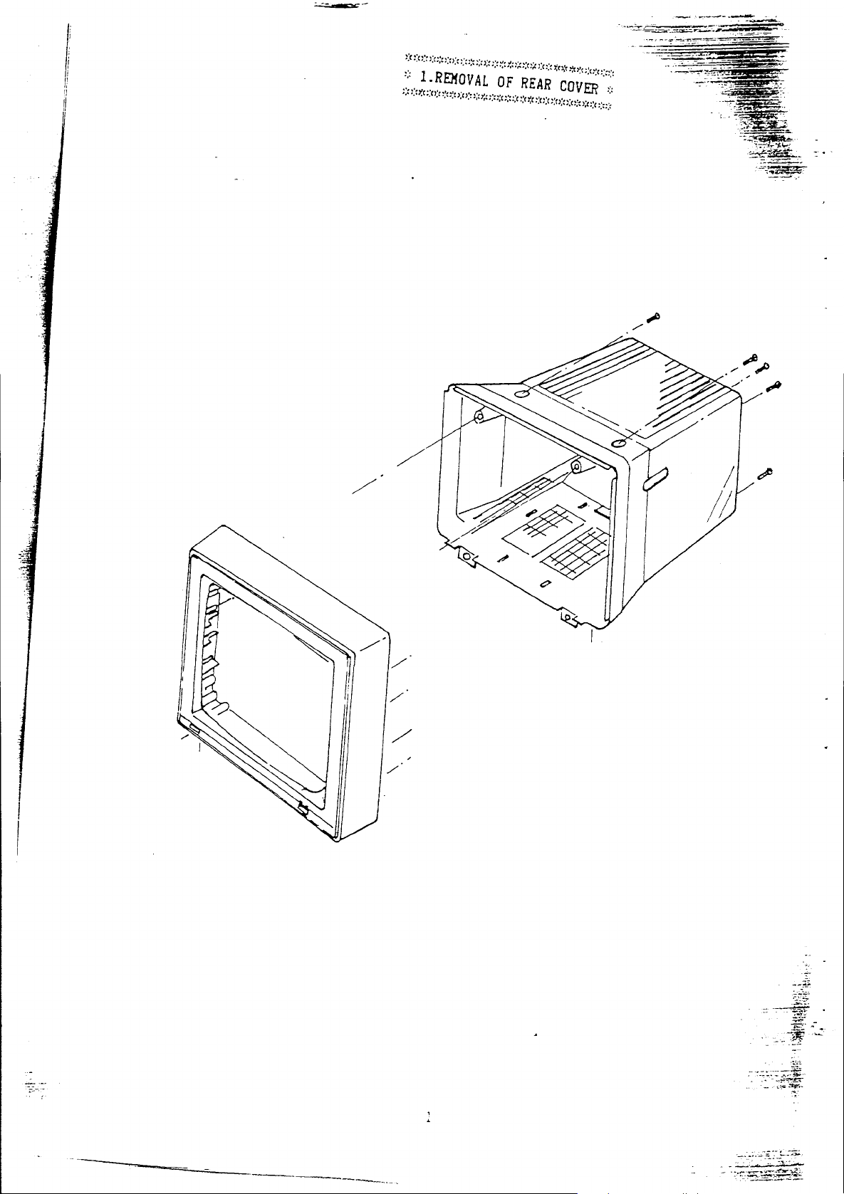
1.REMOVAL
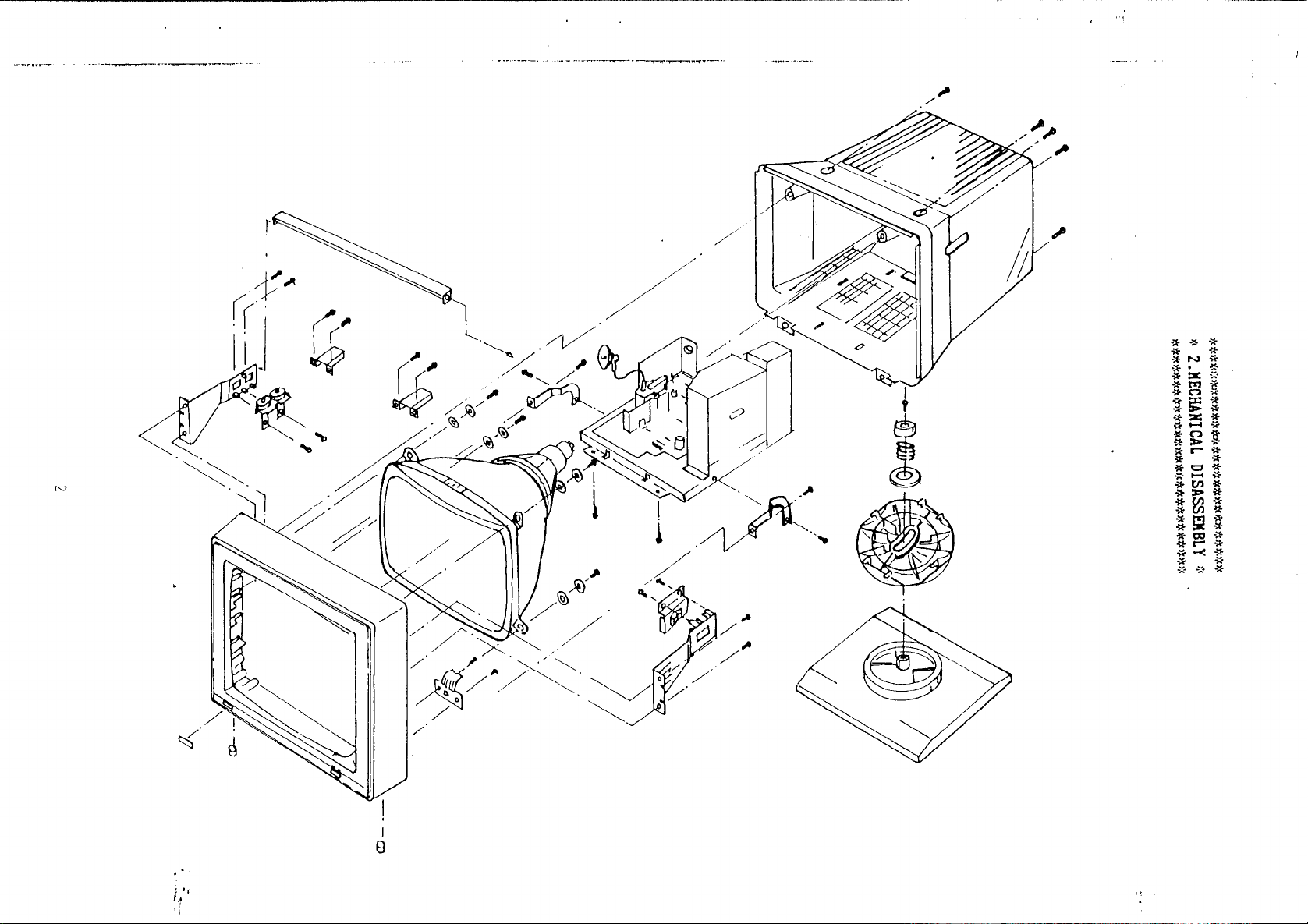
2.MECHANICAL
3.TECHNICAL
4.
5.
DISPLAY
CM-1496X/CM-1498X
OF
REAR
DISASSEMBLY
INFORMATION
GENERAL
DESCRIPTION
5-1
SWITCHING
5-2
AUTOMATIC
5-3
VERTICAL
OF
COVER
OPERATION
MODE
POWER
DEGAUSSING
DEFLECTION
SUPPLY
CIRCUIT
CIRCUIT
SERVICE
CIRCUIT
MANUAL
-
PAGE
1
2
3
4
5
5
6
6
5-4
HORIZONTAL
5-5
DYNAMIC
5-6
VIDEO
5-7
MODE
5-8
SELF-TEST
5-9
SIGNAL
6.ALIGNKENT
7.TROUBLE
8.REPLACEMENT
ASSEMBLY
ASSEMBLY
ASSEMBLY
ASSEMBLY
ASSEMBLY
ASSEMBLY
9.CIRCUIT
PINCUSHION
CIRCUIT
CONTROL
CABLE
PROCEDURE
SHOOTING
PARTS
PCB-MAIN
PCB-CRT
PCB-POWER
PCB-LINE
PCB-LED
CRT
BOARD
LAYOUTS
DEFLECTION
CIRCUIT
CORRECTION
CIRCUIT
PIN
CONNECTIONS
LIST
FILTER
CIRCUIT
6
7
7
8
9
9
10
14
25
25
29
30
32
32
33
34
10.CIRCUIT
DIAGRAM
36
:
,-
Page 3
I
,1
Ii
'I
II
Page 4
/
Ii
~
9
I
I!
•
Page 5
*
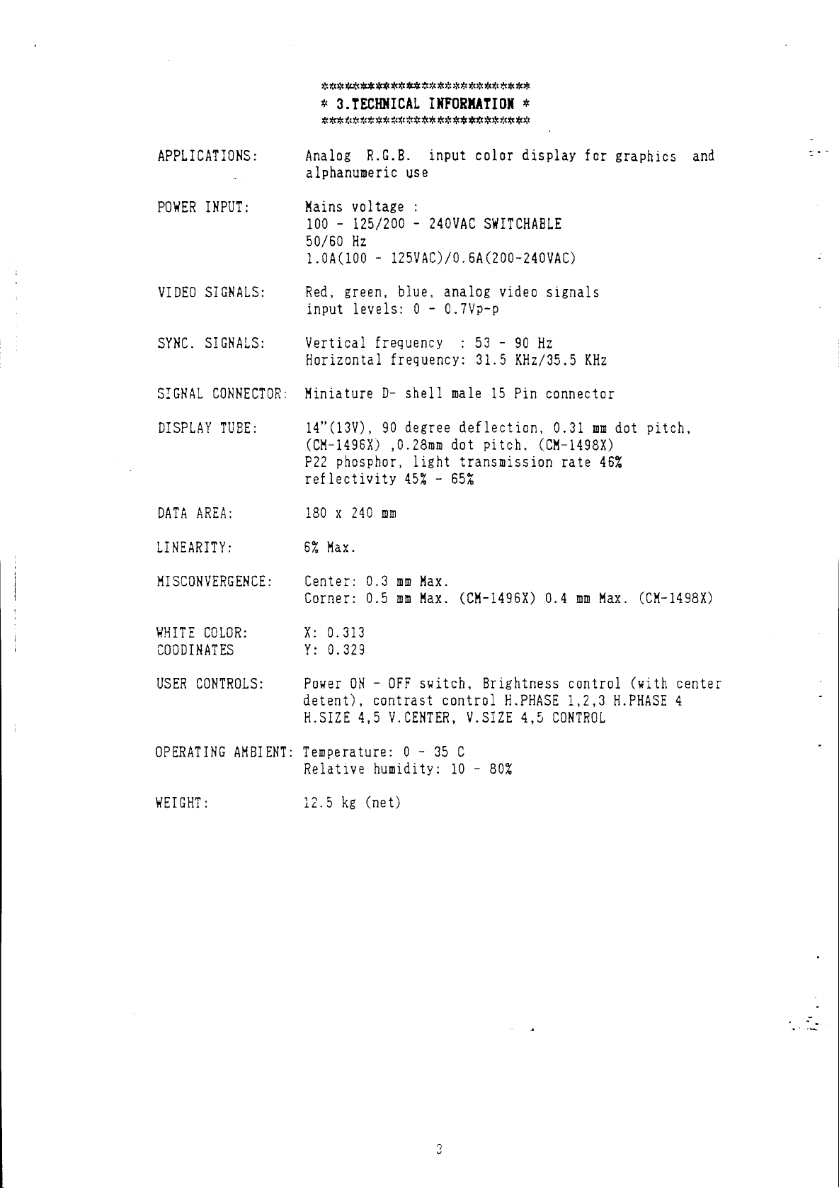
3.TECHNICAL
***f,,*f,(t.:**~,~(;~****~~****~'c~'cf,,**~,
INFORMATION
*
APPLICATIONS:
POWER
VIDEO
SYNC.
SIGNAL
DISPLAY
DATA
LINEARITY:
INPUT:
SIGNALS:
SIGNALS:
CONNECTOR:
TUBE:
AREA:
Analog
alphanumeric
Mains
100 -125/200 -240VAC
50/60
1.0A(100 -125VAC)/0.6A(200-240VAC)
Red,
input levels:
Vertical frequency
Horizontal frequency: 31.5
Miniature
14"(l3V),
(CM-1496X)
P22
reflectivity
180 x 240
6%
R.G.B.
voltage:
Hz
green, blue, analog video signals
D90
phosphor.
mm
Max.
input color display for graphics
use
SWITCHABLE
0 - 0.7Vp-p
shell
degree
,0.28mm
light
45% -65%
53 -90
male
15
deflection,
dot pitch.
transmission rate
Hz
KHz/35.5
Pin connector
0.31
(CM-1498X)
KHz
mm
dot pitch,
46%
and
IHSCONVERGENCE:
WHITE
COODINATES
USER
OPERATING
WEIGHT:
COLOR:
CONTROLS:
AMBIENT:
Center: 0.3
Corner: 0.5
X:
0.313
Y:
0.329
Power
detent), contrast control
H.SIZE
Temperature: 0 -
Relative humidity:
12.5
ON -OFF
kg
mm
mm
4,5
V.CENTER,
(net)
Max.
Max.
(CM-1496X)
switch, Brightness control (with center
V.SIZE
35
C
10 -80%
0.4
H.PHASE
4,5
CONTROL
mm
1,2,3
Max.
(CM-1498X)
H.PHASE
4
.-
Page 6
*************
*
4.GEMERAL
*
~=~---*
CM-1496X/CM-1498X
dot pitch
signals
text
display.
It
is
various industry graphic standards such as, the
800X600,
sizing
to
l024X768.
A
self-test
from
cted
white
with a
CRT
and
TTL-level seperte sync.
designed to provied
IBM
circuitry
pattern
the driver source.
raster
vertical
is a high
with etched
8514A
extending
black bar
l024X768
that
provides automatic
shall
resolution
faceplate.
you
be
available
The
beyond
on
the
color display using a 0.31/0.28
Analog
signals
with a
and
self-test
the display bezel at the top
left
wide
incorporates the automatic
when
and/or
are adopted for graphic
range
sizing
the signal cable
pattern
right
16-1evels
of
compatibility with
IBM
VGA
PS/2, super
resolution
will
consist
edges.
R.G.B.
of
640X350
is
and
ma
video
and
VGA
vertical
up
disconneof a full
bottom,
4
Page 7
5-1
SWITCHING
The
s~itching
~ormal
case
and
a secandary voltage
A.
The
follows:
1.
aui
The
effects
the switching
~
Enabling
Simultaneously with
becomes
exceptIon
resistant
3.
Enabl
In
current supply for the control
additional
ready for operation.
,;<
5.
MODE
- .
TDA4601
POWER
is
transistor
and
overload operation as well as during disturded operation . In
of
disturbance the drive
SUPPLY
designed for driving
in flyback converter
rise
start-ur
ld-ur
procedures include three consecutive operating
internal
ref erence vol tage
DESCRIPTION
CIRCUIT
of
IS
prevented.
OF
OPERATION
controlling
power
the switching
intenal reference voltage supplies the voltage
charging
of
the coupling
electrolytic
transistor.
of
internal
available providing
of
the control
voltage reference voltage
va
reaching approx
all
lOgIC
with a thermally
12V.
component
current supply.
ing
of
control lagH
conjunction with the generation
stabilization
circuit
of
lOgIC
The
the reference voltage.
is
activated
Integrated
,;:
and
protecting the
supplIes during
transistor
is
start-up
inhibited
phase
regulator
capacitor cannected to
Vl=4V
an
Internal
voltage
elements. with the
stable
and
by
means
circuit
overload
of
is
as
and
The
an
then
B.
Normal
At
feedback
( control input overload
~ectified
amplifier operates with
a~prox
The
current simulator Pin 4 the operating range
The
at
collector
propovtion
range
b~tween
voltage
operation mode/control operation
the input
of
coil
Pin
2 the zero passage
~re
registered
and
1.4mA
overload
collctor
Pin
4
amplitude
depending
identification
current is sImulated
and
internally
fluctcations
an
input voltage
on
the
set threshold voltage
current applIcable with the switching
to
~he
of
the control
a
DC
WhICh
increased
voltage
can
vary
arnplifie~
~apactance
clamped
up
to a
mode
of
the frequency provided
and
forwarded to the control logic Pin 3
standing
internal
limits
by
identification)
of
the feedback
of
approx
voltage reference.
in conjunction with
of
the control amplifier
an
external
RC
The
transistor
caos
thus the reguired operatIng
is
established
at
2V
and
max
amplitude
the range
a
sa~tooth-snaped
of
4V
during secondary load reductlon the switching frequency
and.
Ie,
are present at
A~d
to
R804
resistor
the
Pin 5
~t
is possible
the outp;.it:1.t ?in 8
PIn
5.
the
bas~
current amplifler forwards the sawtooth-shaped
the output
1S
of
present
Pin
6.
between
determines the
switching
transistor.
to
4i11
externally
be
Inhibited
inhibit
when
A current feedback with
Pin 8 and
max
amplItude
Pin
of
7,
the
volltage
an
the applIed value
base
by
the
receives the
coil
2V
the control
and
a current
collector
combinatIon present
largest
possible
increase in
of
control
lies
rising
(reference voltage)
is
increased
the operatlon
of~Vref
external
of
V4
voltage
resistor
of
the
-O.IV
the
driv1ng current for
of
AC
C.
Protective
The
base
outpu~
~r~~:sistor
supply
of
voltage
operation
mode
current shut-down
l.
61,1
P
i;l
7 to
1S
inhibited T his
a:
Pin 9 reach'Os
.
activated
As
a
result
protective
a
va
lue~6.
5
by
the
control logic
drive
the
measure
7
V
or
if
clamps
of
the switching
is
enabled
vol
tage at
if
.::;;:
the
the
Vre~
2
...
....
-.:
-
Page 8
-O.IV
5-2
AUTOMATIC
a~e
present
DEGAUSSING
at
PIn
CIRCUIT
5.
Posistor
(ADG)
R803
circuit
and
degaussing
to demagnetic the
CRT.
Posistor
line
seconds,
degaussing current thus decrease to
function
5-3
VERTICA~
The
R343.
running frequency
The
mirror
Pin 9
C305
Pin
Pin
shows
low
voltage. current
resistance
is
completed.
DEFLECTION
vertical
C310
resistance
and
of
and
10
of
12
of
sync. signal is applied to Pin 5 & Pin 4
connected to
of
between
then the height
Q301
is
output
C306.
This
Q301
is the output
Q301
is the inverting input
resitance value in normal temperature.
of
about
of
posistor increase
CIRCUIT
Pin
the
oscillator
Pin 7
of
of
the
Pin
is
also the input
coil
L991
compose
shadow
20
Ap-p
mask
flows into degaussing
rapidly
less
3,
Pin 4
inside
of
0301
and
the scanning.
current
of
the buffer stage.
mirror
of
the amplifier.
an
Automatic Degaussing
and
internal
due
than
120 m Ap-p,
and
Pin 6 determin the
to
shield
when
rising
of
Q301.
in the
apply
coil.
after
in heat,
degaussing
R342.
free-
Q301.
ground defines the current
that
of
buffer stage.
changes the
series
AC
of
R307
centering
and
the parabola. available across
across
output
The
deflection
used
The
and
R310
define the
of
the output voltage.
R310.
applied at the feedback input Pin
R312. R305,
scanning current.
output
of
po~er
yoke
to
stabilize
supply voltage
DC
level across
R308
C309.
R30B
and
R310
produce the
amplifier
by
a negative slop current ramply.
the
po~er
of
the
from
amplifier.
power
output stage
the trace tlme the supply votage IS obtained
by
D301.
internal
Pin
15
from
~ump
to Pin
Pin
14
5-4
HORIZONTAL
The
positive horizontal sync. pulse
amplified ty
/
R403
while
dUrlng
flyback generator.
is
the output
lo~
to
high
condition.
2.
of
Q301
is the
DEFLECTION
to
Pin 3 of
Q406.
Then
the
the
retrace
of
the flyback generator
An
external
main
supply voltage input.
CIRCUIT
be
applied through the
horizontal
Ie
C309,
and
and
the
the Pin 1
time
this
capacitor
from
Pin 6
Q402.
so
allowing a correct
C308
in conjuction with
12
of
0301,
AC
feedback voltage, taken
linearity
of
Q301
is
forced at Pin
from
the
a small part
correction
drives the
R309
and
main
supply votage
Pin is supplied
that,
differential
of
when
C304
Q201
driven.
transfers
is
converted
circuit
on
vertical
C307
2.
During
from
R307
of
the
are
the
jumps
the
and
C407
The
positive
~ntegrated
horizontal flyback pulse derived
by
the comparable
from
Pin 5
sa~tooth-waveform
6
generator
of
FBT
which
T403
is
is
com-
Page 9
posed of
Pin 4
The
ween
the supper
R410,
of
0402.
discriminator
the sync. input
imposed
low-pass-filter
R406
via
The
to Pin 7
oscillator
the timing.
horizontal
The
predriver output
led
by
oscillating
R402
and
R411. R423.
inside the
pulse outRut
R407,
of
Q402.
inside
R404,
R405.
of
R403
at
C408.
from
Pin 3
C404
and
thereby
IC
Q402
R422,
frequency.
Q402
is
Pin 8 of
IC
from
C403,
is
at
Q402
and
an
C402
0402.
and
C410.
detects
the sawtooth-waveforme
Pin 5
AFC
controlling
RC
and
Pin 1
then
be
applied via
the phase
difference
from
of
0402
is
integrated
voltage
is
the
oscillator.
obtained
type with Pin 7 used to control
C410
of
altogether
which
duty cycle
determine the
and
is
control-
C405
to
betPin 4 .
by
the
applied
Regulated voltage applied
The
output signal
coupled
by
T401
to
the horizontal output stage
from
at
Pin 6
Pin 1
of
of
0402
Q402
is
is
then amplified
thus sawtooth-waveform current through the horizontal
obtained.
Also during the
retrace
flyback pulse at about
this
voltage
5-5
DPC
The
raster
The
R326, R327,
pulse
of
about
CIRCUIT
Side
Dynamic
width
vertical
is
transfered
22.0KV
Pincushion Correction
as
a function
castle-waveform
R328,
for side pincushion correction,
Q302
and
Q303
stages
able
The
reactor
inductance
T402.
of
parabolic current.
horizontal
deflection
the
time
of
the
1100
volts
and
rectified
tor
anode
ot
vertical
from
C316
etc.
to
and
then
T402
this
output winding is
drives
output winding
yoke.
horizontal
is
produced
by
the
of
CRT.
circuit
deflection.
Pin 1
of
produce a parabolic
this
parabolic voltage
the control winding
is
about 8 - 9
Q403
deflection.
at
the
FBT
T403
(Side
0301
is
modulated
inserted
volts.
by
for
ON-OFF
deflection
a horizontal
collector
to obtain high
DPC)
modulates the
integrated
waveform
is
amplified
of
the
by
the
in
series
Q401
and
control,
coil
is
of
Q403.
by
C314,
necessary
by
satur-
vertical
with the
The
to
5-6
VIDEO
The
color.
:dentical.
Video
and
The
Analog
to input
Contrast is
Pin 7
horizontal
correct
yoke
current
side pincushion
is
th8n modulated
distortion.
CIRCUIT
color display contains three video
amplifiers,
these three amplifiers for the red, green
amplifier
consists
of
preamplifier
cut off adjustment CIrcuit.
operation
video signals IS preadjusted
of
of
FBT
of
only
Q501.
DC
controlled
(T403)
to
one
channel (blue) is described here.
by
R502
from
Pin
14
of 0501.
PIS
of
0501.
The
7
Q501
and coupling
output
by
the
correction
one
and
blue
(H51387P),
clamp
of
pulse provided
Q501
is
voltage
for each primary
CRT
guns
are
output stage
VIA
C501.
C502
from
at
Pin
21.
Page 10
C504
The
is
B+
used for
of
preamp.
clamp
(12V)
pulse to charge.
and
output stage
is
provided
from
S.M.P.S.
5-7
"The
co~posite
clamp
MODE
(1)
the Blanking level
CONTROL
HORIZONTAL
H.Sync.
(F/V
1.
So
and
"LOW"
control
(2)
HOR.
WIDTH
When
Hf=31KHz,
is
"V',
90VDC
105VDC
change
as
Hor.
(3)
HOR.
OSC.
When
Hf=31KHz,
then
#12#14#
the time constant
blanking pulse
CIRCUIT
FREQUENCY
pulse with
CONVERTER)
we
get a
when
Hor.
Then
"HIGH"
Hor.
width,
CONTROL
Q212#1
QE801#B
was
is
sent to
the
base
width
FREQ.
sent
current
when
CONTROL
is
to
Q212#1
are connected.
of
is
to A suitable
DETECT
different
there
freq.
Hor.
"L",
FBT
FBT#9
at
osc.
is
#9.
and
of
ar-e
Pin 1
is
"H",
QE801
QE801.
Hf=35KHz.
is
"H".
Hor.
osc.
provided
position.
frequency
different
of
Q212
35.5KHz.
freq.,
Q209#C
cutoff,
When
Hf=35KHz.
DE801
is
then
Q209#C
When
Hf=35KHz
circuit
from
vert.
was
voltage
when
This signal
Hor.
phase.
is
"L",
then
cutoff.
change
is
"L".
Q203#13#14
will
circuit
sent to Pin 6
at
the output Pin
Hor.
freg.
can
Q214#C
DE801
QE801
is
is
is conducted
Adjusting
the output
Q203#9#10#11
are connected,
be
changed.
to
Q407.Gl
of
is
31.
be
used
"H".
QE802#C
conducted
RE810
of
QE801
is
Q211_
5KHz
to
and
and
can
so
"L",
(4)
HOR.
When
connected.
(5)
VOLTAGE
Q201
posltlve.
get a
"H".
reference).
sync.
MODE
1 +
MODE
2
MODE
3
(6)
SIZE
Q208
Q209#C
picture size
"H".
disabled.
PHASE
CONTROL
Hf=31KHz,
AT
POSITIVE
74LS86
#3
"L"
at
pointHD.
It's
the
The
H.SYNC.
CONTROL
OF
74LS138
is
"L".
of
so
that
Since
Q203#15#2
is
an
also positive. This pulse
same
output
V.SYNC.
+ H
MODE
is
a 3-to-8 decoder (Multiplexer).
0205
mode
Q208#13#14
Q214#C
are connected.
END
.OF
C204
XOR
LOGIC
However
condition
at
POINT
3
is
conducted. Adjusting
3.
From
are
is also
When
(POINT
IC.
"D")
If
the input pulse
will
a negative pulse
at
point
#8
and
#6
are
"D"
L
H
table 1 we
"H".
"H"
POINT
H
L
H
can
D202/0204
R241/R207
Hf=35KHz.
and
C203
be
filtered
will
HE".
always
Q203#15#1
(POINT
be
(See
HE")
of
by
filtered
tabe 1 for
are
#2
C204
as
positive for easy
"E"
know
TABLE
R315
that
1
When
can
Q208#1#2
fH=31KHz.
vary the
are cutoff R208/R211 are
are also disabled too.
is
to
a
are
(7)
SIZE
From
Adjusting
adjusting
(8)
SIZE
CONTROL
table
OF
1.
R208
R208
CONTROL
OF
MODE
DIE
can
vary
since
MODE
2
are
picture
R208
1
H/L,
is
Q208#14
size
parallel
8
is
"L".
R315.has to
to
R315
now.
0202
are conducted.
be
preseted before
.-
Page 11
Q2081l3
(9)
SIZE
Q304(PWB-1627)
delay the sync. pulse.
around
voltage.
0305#C
available
fH=35KHz)
(10)
SIZE
When
There
condition,
have
disconnected
adjusting.
SELF
5-8
Self
via
with black
is
connected
a dark screen.
is
CONTROL
11.6mS.
is
CONTROL
the period
is a negative pulse at
enough
TEST
test
signal suppied
R214,
R215,
vertical
"L",
R211
is availabe
OF
KODE
4
74LS123
When
We
The
DC
voltage
,
0210tC
parallel
in series to
OF
MODE
5
of
sync. pulse
will discharge
"L
and
and
n
C322
voltage
and
R207
from
R216
to
bar
on
to
a system unit the
and
is a
monos
table multivibrator.
In
mode
4,
delay
is
from
"H",
to
that
Pin 5 will
then
R340,
pulse for 11.6aS,
0213#14#13
R241.
is
much
0304#5.
by
the
to
saturate
is disabled.
heater buffered
the video input
the
left
and/or right edges.
collector
parallel
the period
make
(R241
is
longer than
way
0305
Only
by
to
generate
of
to
R315
of
vertical
Q305
saturated.
are connected.
always
11.6mS
Once
of
Then,
the pulse
D312 . So,
R241
is
0205,
Q213#14#13
0206,
full
When
0204
is
grounded
We
use
it
sync. is
it
becomes a DC
When
R207
available
(e.g
when
18mS)
in
C322
cannot
will
available for
0207
white screen
the display
to
make
to
is
"L"
and
5-9
SIGNAL
Pin
1
2
3
4
5
6
7
8
CABLE
PIN
CONNECTIONS:
Signal
------ ------
Red
Signal 9
Green
Blue
Jumper
Signal
Signal
tD
Pin
10
Self-test
Red
Return
Green
Blue
Return
Return
Pin
10
11
12
13
14
15
Signal
No
Digital
Jumper
No
Horizontal
Vertical
No
Pin
Pin
Pin
Ground
to Pin
Sync.
Sync.
10
.-
9
Page 12
':.
6.
Al.l
GMMEMT
6-1
o
5
1
EQUIPl'IENTS
1.
Manual
2.
DSClll.Qscop~
3.
D~gi!al
4. Color a:1alyzer
5.
Pdt:'
6.
EHT
meter with high voltage
5-2
POWER
SUPPLY
degaussing
+
probe
vcltmeter
OUTPUT
coil
VOLTAGE
PROCEDURE
probe
l~
Connect a DVM
means
6-3
VERTICAL
of
Connect
to S.K.P.S. output red wire adjust the voltage to
R813.
FREQUENCY
a frequency counter across the
the frequency.
disconnected
6-4
HORIZONTAL
Use a test
and
R405(35.5KHz)
6-5
PINCUSHION
Straighten
6-6
WIDTH
~djust
6-7
VERTICAL
from
FREQUENCY
pattern.
the side
the
data
CENTERING
Center the data area with
To
49Hz
the
Without
to
get the color bar in
lines
area width
PC.
by
means
horizontal sync. input. adjust
with
to
240
R338.
R327
+/-
of
and
vertical
R314.
an
R328.
5
mm
using
deflection
the
signal
upright
L402.
coil.
cable
R422(31.5KHz)
position.
(fH=31.5KHz)
90V
adjust
must
by
be
6-8
VERTICAL
~cjust
6-9
HEIGHT 3 (480
LINEARITY
the squares equal in height with
Adjust data area height
6-10
HEIGHT 2 (400
Switch
with
6-11
HEIGHT 1 (350
Switch to
with
6-12
HEIGHT 5 (600
to
R208.
150
R211.
lines)
to
lines)
400
lines
(Be
sure that height 3
mode. Adjust data area height to
lines)
lines
(Be
mode
sure that height 3
lines)
R316.
180
+/-
5
mm
with
R315.
has
been
adjusted)
Adjust data area height to
has
been
aajusted)
10
180
180
+/-
+!-
5
5
mm
mm
.-
Page 13
Switching to
wi
6-13
HEIGHT 4 (768
th
R241.
600
lines
lines)
mode. Adjust data area height
to
180
+/-
5
II
Switching
with
R207.
6-14
FOCUS
ADJUST
Adjust
6-15
WHITE
Turn
X/Y
the brightness
minimum.
Turn
the sub-brito
-25V.
Turn
the
disappears.
Turn
the
achieve
0-5
F.L.
Use
full
at
detent,
coordinates.
to achieve correct
to
768
FBT
lines
(Be
sure that height 5
focus
VR
mode
to
get best
VR
Set cut-off drive
VR
R443
G2
control to a position
brightness
VR
to
the color coordinates
field
white pattern, turn the
adjust
Then
R502,
turn contrest
X,Y
coordinates.
Adjust data area height to
has
been
adjusted)
overall
to
center
VR
R910/R940/R970
to a position
max.
and
X=0.313
focus screen.
detent
position,
to center.
where
where
to get the brightness
adjust
the
Y=0.329
contrast
R532
and
VR
R562
to get
to achieve the correct
3J.L.
contrast
to get the
R910,R940
roughly
to
maximum,
Adjust
180
+/-
5
mm
VR
to
Gl
voltage
is
just
and
and
brightness
R970
to
brightnes
X,Y
R910/R940/R970
F/V
6-16
Adjsut
between
INTERLACE
6-17
CONVERTER
R235
Q212#3(+)
ADJUSTMENT:
VR
to get
and
ADJUSTMENT:
Receiving 1024x768(interlaced)
Adjust
R218
so
that
(MODE
0.7V
Q212#2(-)
small "s"
3,
FULL
+/-
0.1 between
after
signal,
is
not
WHITE
SIGNAL)
#P2
warm
up
the
display small
distorted.
(+)
set
and
for
"s"
character.
#P1
20
minutes.
(-)
or
.-
11
Page 14
I.
IBm
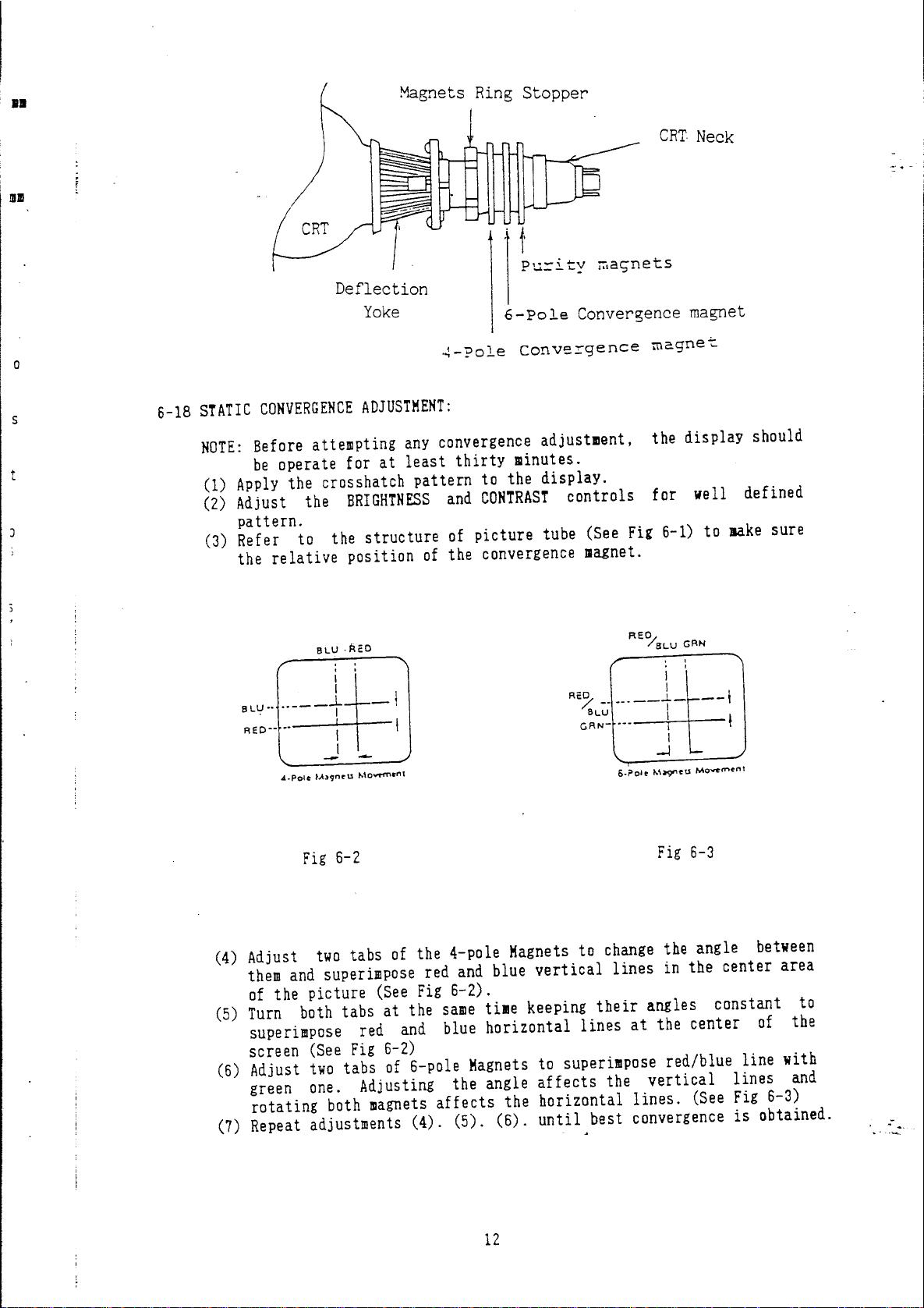
Magnets Ring
Deflection
Yoke
Stopper
6 - Po
CRT
le
Convergence magnet
Neck
~-?ole
o
6-18
5
STATIC
NOTE:
t
(1)
(2)
(3)
CONVERGENCE
Before
be
Apply
attempting
operate for
the crosshatch pattern to the display.
Adjust the
pa
ttern.
ADJUSTMENT:
any
at
least
BRIGHTNESS
Refer to the structure
the
relative
. I
",U"
..
REO·-
--
_.
position
BLU
.RcD
+f
I
I
-
--
of
I
I
convergence adjustment, the display should
thirty
and
of
the convergence
convergence
minutes.
CONTRAST
picture tube
magnet
controls for well defined
(See
Fig
6-1) to
make
sure
magnet.
RED
/SLU
GAN
RcD
;(
_.
__ • __
r=ff="
BLU
GRN-
---
I
..l._
--I
I
I I
I
-l
Fig
(4)
Adjust
them
and
of
the picture
(5)
Turn
both
superimpose red
screen
(6)
Adjust
green
rotating
(7)
Repeat
6-2
two
tabs
of
superimpose
tabs at the
(See
Fig
two
tabs
one.
Adjusting the angle
both
magnets
(See
6-2)
of
and
6-pole
the 4-pole
red
and
Fig
6-2).
same
blue horizontal lines
affects
Magnets
blue
tile
Magnets
the horizontal
adjustments (4). (5). (6).
12
Fig
6-3
to
change
vertical
keeping
to
superimpose red/blue line with
affects
until
lines
their
the
best convergence
the angle
in
the center area
angles constant to
at
the center
vertical
lines.
lines
(See
between
of
Fig
6-3)
is
obtained.
the
and
.-
Page 15

6-17
TIMING
HORIZONTAL
CHARTS
VERTICAL
PRE-SET
fH
Aus
Bus
Cus
Ous
Eus
Fr
OilS
Pms
QIIS
Rras
Sms
14.27
0.064
1.88
11.126
1.2
VIDEO
-J
Q
1-
U
-i~
TIMING
VGA/PS2
COMPATIBLE
31.5
KHz
31.
77
3.77
1.
89
25.17
0.94
70Hz
14.27
0.064
1.
08
12.716
0.41
15.246
0.35
R
o
60Hz
16.68
0.064
1.
02
'--1_---'
..
I~
U.----
..
/
SYNC.
8514/A
COMPATIBLE
35.52KHz
28.15
3.92
1.
25
22.8
0.18
87
11.5
0.113
0.563
10.81
0.014
POLARITY : POSITIVE/NEGATIVE
800X600
35.16KHz
28.44
2
3.56
22.22
0.67
Hz
56
17.78
0.06
0.6
17.07
0.03
Hz
SEPARATE
REMARKS
H.SYNC.
POSITIV
V.SYNC.
NEGATIVE
SYNC.
SEPARATE
SYNC.
H.SYNC.
NEGATIVE
V.SYNC.
POSITIVE
SEPARATE
SYNC.
H
.SYNC.
NEGATIVE
V.SYNC.
NEGATIVE
13
INTERLACED
SEPARATE
SYNC.
H.SYNC.
POSITIVE
V.SYNC.
POSITIVE
NEGATIVE
SEPARATE
SYNC.
H.SYNC.
NEGATIVE
V.SYNC.
H.
SYNC.
POSITIVE
V.SYNC.
POSITIVE
.-
.-
Page 16

i
I ..
_'C,-
No
Raster
f:·.;,:,::::'EF'~
i
t
i
!
Check
90V
Line
OK
******#*******~~******
l~
7.
TROUBLE
SHOOTI.;
*
**********************
..--
Measure
NG
90V
Pin on the Main Board (PWB·1561)
Check H. V.
OK
Check
Check
12V
OK
CRT
OK
Operation
Line
Heater
-I
NG
NG
NG
Check the SMPS
Check
0402,0401,
Check the SMPS
Check
6.3V
Pin
(pWB-1299B)
OK
Unit
0406
Unit
on the
H. V.
Output
PWB-1345A
Video
Drive Board
1
Circuit
NG
I
I
I
I
Turn
the Screen (R448)
Control
Check the Screen Voltage
Clockwise
OK
r--
::1
NG
----
6.3V
Line Failure Connect the
Check SMPS
T403
FBT
Unit
Unit
-
Failure
.
CRT
Failure
PWB
1299B Failure
14
or
Video
Drive Board
Line
from
6.3V
SMPS
1
.-
Page 17

No
Picture on the
Check the Signal Connector
on
the- Personal
CRT
Computer
OK
Check the Signal Housing
P901
on
PWB-1299B
OK
Check
,.
,:
PWB-1299B
OK
12V
Line on
!
I
NG
NG
NG
Lock
the Signal
on
the
Personal
Connect
P901
Check SMPS
Signal Housing
on
PWB-1299B
Connector
Computer
JOK
0K
1
12V
to
Line
Check Clamping Pulse
PWB-1299B H. Pin
OK
PWB
Check
1299B
Q501
on
I
NG
Check PWB-1561 O. Pin
.-
15
Page 18

SMPS
NO
Action
]
Check
Fuse
OK
Oa01
Check
OK
Check
Check B + =
Check
Ra08
OK
OK
0803
OK
on PWB·142aA
Ra10
250V
- 350 V dc
NG'
NG
NG
NG
NG
Replace
Fuse
I I
Replace
0801
I I
Replace R80a. Ra10
I I
Check Rectifier Ckt.
Replace Oa03
I
I
I
I
~
I
Check
Check IC801
Oa20 -0824
OK
OK
Check IC801
OK
NG
I I
#5 ~ 2.5V?
NG
I
:::::
2.5V? Check Ra16
#2
NG
I
Replace Oa20 - Oa24
Check Ra05
I
I
Replace ICa01
.-
16
Page 19

Abnormal Vertical Height
Horizontal
y
Check
20V
OK
Line
Line
N
NG
Too
High or
Check SMPS
Too
20V
Low
Line
Check Fusiable R320
OK
Check
0306,
0307,
R340, Q301
Check, R304, R340, R312, R208,
R207, R241, R211,
R315
17
Page 20

r
-"--
-_.
-.
Abnormal Hor Width
t
J -
Check
!
f~-'~;'-
,
OK
Re-adjust
OK
B
+
90V
-
L402
Line
NG
NG
I
Adj
R813 on
PWB-1345A
Replace
L402
I
Check L403, R420,
OK
Check RE810, Q214
QE801, QE802
C422
18
.-
Page 21

Unstable Synchronization
(A)
Horizontal
sync.
i I
I
Check H .
Check PWB-1561
0201
OK
Check PWB-1561
0201
..
#5
#6
Sync.
H. Sync.
H.
Sync.
Intput
NG
Output
Check
or
Signal Cable on Personal Computer
P403 on Main Board PWB·1561
OK
Check
C402,
0402,
R427, R445
0406,
NG
R404
Check PWB-1561
I
0203
I
19
Page 22

i
.----.
t
.::......
t
~
I
.~,-
..
.§
·~-.fi~.L..
.
~,.--
,
....
-
(6)
-
..
Check
!-.
...
,.,..
.'':'-~~.-
.
Vertical
V.
Sync.
I
sync.
-
i
I
;
I
!
r
Check PWS-1561
v.
OK
V. Sync.
OK
Sync.
Output
#12
Check PWS-1561
#8
0201
Input
0201
NG
I NG
I
Check Signal Cable on Personal Computer
or
P403 on Main Soard PWS-1561
Check
PWS-1561
0202
·1
I
f
~
,
I
Check
Q301, R301,
R311, C311, C310
C301
.-
20
Page 23

Abnormal Color Display
No
Color
Display
Check B +
OK
[ Check 0501
12V
P901
Line
•
One or
Check
Computer
Check
#3,
Check
R,
#21, #25,
Two
Signal Cable on the Personal
0501,
#7,
OK
0501
G, B
Output
and
#11
Color
Chassis
OK
R,
#29
G,
Missing
B,
Signal
Input
NG
Check
0501
# 13 B+
R502, R532, R562
OK
Check
P502
OK
Check
0932, 0961,
90V
0901,
NG
on
NG
0902, 0931,
0962
Replace
Check
Q501
SMPS
1.-
'1-
.
21
Page 24

...
~-------
Abnormal Side Pincushion Distortion
Re-adjust
Check
R326, R328, C316,
R327
-
NG
T402, Q302,
Q303
R336
\
~
i
l
!
.-
22
Page 25

Abnormal 31.5 KHz/35.5 KHz
Check Q211 :I; 8
12.5
±
1V
NG
Chage
Check
on PWB-1561 P802
12V
Line
Check
SMPS
Check
VP
(31.5 KHz)
OK
Check PWB·1561
Q211, Q212. Q209
Q214, QE801, QE802
1
==
VP~
:f: =
+ 0.5 ±
0.1V
NG
Re-adj
on PWB-1561
R235
23
.-
Page 26

Abnormal Contral Board
(A)
Abnormal
Check Q201
MODE
#12
1 -
MODE
V Sync.
(PWB-l0l)
5 Vertical Height
OK
Check
0205,
OK
Check
Q208,
0208
Q212
NG
0202,
0204
NG
#1 H (31.5 KHz)
NG
Replace Q201, Q212,
Q206
(B)
Check
#P2,
Check
Abnormal
PWB-1561
or
OK
Q203
31.5 K
Q212
Hz/35.5
#P1,
#1
NG
KHz
Hor Hold & Hor
24
Phase
Change
Check
R404, C416
0212
or
Q402
.-
Page 27

,;,
8.REPLACEMEM"!
PARTS
LIST
'::
- ,
..
-=-:...:~=.,-
.-
"::'-?-7i:"':
',C203,C204
.•
~?~,i~_.
...
,;
....
09.
ARMING:
Replacement parts
ety should
it
or
omponents, read
he
safety
of
-------------------------------------------------
CAPACITOR
5222110391
C202
5~13410191
5213247091
"
,
,
,
,'"
C206
C207
C210
C211
C212
213,
C305
5222110491
5222115391
5213622891
5221115291
5242210191
5222110491
C306
-
C302
,
C303
C304
C307
C308
C309
C310
C311
C312
C313
C314
C3l5
(316
C317
C3lS
C319
(320
C323
(401
C402
(403
C404
C405,
C406
(407
C408
C409
[410
[411
C4
5213510213
5236310401
5213622112
5222410401
5213247091
5213410213
5275233401
5222110491
5214410012
5214247991
5213510091
5232710301
5213522091
5:13410091
5213233112
5247068191
5213447091
5213410091
5213447112
5227330291
5221156291
5213601091
31
5221110401
5221110391
5231310291
522:147291
~247015191
5221147291
5213322191
which
be
replaced only with types
specified
in
the
carefully
have
parts
the product
the display through improper
PAR';
NO.
DESCRIPTION
ASSEMBLY,PCB-MAIN,
CAPACITOR,POLYESTER
CAPACITOR,ELECTROLYTIC
CAPACITOR,ELECTROLYTIC
CAPACITOR,POLYESTER
CAPACITOR,POLYESTER
CAPACITOR,
ELECTROLYTIC
CAPACITOR,POLYESTER
CAPACITOR,CERAMIC
CAPACITOR.
POLYESTER
CAPACITOR,ELECTROLYTIC
CAPACITOR,BARRIER,LAYER,CG45X F DC
CAPACITOR,ELECTROLYTIC
CAPACITOR,POLYESTER
CAPACITOR,ELECTROLYTIC
CAPACITOR,ELECTROLYTIC
CAPACITOR,METALLIZED
CAPACITOR,POLYESTER
CAPACITOR,
ELECTROLYTIC
CAPACITOR,ELECTROLYTIC
CAPACTIOR,ELECTROLYTIC
CAPACITOR.
CAPACITOR.
CERAMIC
ELECTROLYTIC
CAPACITOR,ELECTROLYTIC
CAPACITOR.ELECTROLYTIC
CAPACITOR,CERAMIC
CAPACITOR,ELECTROLYTIC
CAPACITOR.
CAPACITOR.
ELECTROLYTIC
ELECTROLYTIC
CAPACITOR.POLYPROPYLENE
CAPACITOR,POLYESTER
CAPACITUR,ELECTROLYTIC
CAPACITOR.POLYESTER
CAPACITUR,POLYESTER
CAPACITOR,CERAMIC
CAPACITOR,POLYESTER
CAPACITOR,
CERAMIC
CAPACITOR,POLYESTER
CAPACITOR.
ELECTROLYTIC
special
identical
list.
safety
servicing.
PWB-1561-03
CC45
P=7.5MH
P.E
CK45
CC45
P=7.5MH
CK45
CC45
characterist
to those
Before replacing
precaution
SPEC
CQ92M
CE04W
CE04W
CQ92M
CQ92M
CE04W
CQ93M
CH
DC
CQ92M
CE04W
CE04W
CQ92M
CE04W
CE04W
P=5MM
CF93M
CQ92M
CE04W
CE04W
CE04W
E
DC
CE04W
CE04W
CE04W
SL
DC
CE04W
CE04W
CE04W
C093T
CQ93M
C~04W
CQ93M
CQ93M
B
DC
CQ93M
SL
DC
CQ93M
CE04W
'
_
-:~~2t.¥t~:::;~.
--'~~;:.,;:.::.:..---
-
.-~~~~~~~~-.:~
~.'--.,..~~-.
-
--~::~~-'-.
;,',.i:;;~,
...
_
.-~Y:.;:l~:
~
50VIOOOO.OOPFJ
25V-::;ioo-.OOUFM
IOV
::~47:
OOMFM
50V
"~PO::IOMFJ
50V15000.00PFJ
SOV
SOV-1500:00PFJ
50
50V~~2~-o:1
-.·
--.';~'f:t.=~~--:~-.-
35V;1000.00UFM
50V
50V
100V
10V --47.00MFM
25V
63V
50V"~·~·
250V_'~'
160V
35V --10.00UFM
500VIOOOO.00PFP
35V
25V.
10V
SOV
25V'25V
25V
lOOV
50V
50V
SOV.
50VlOOOO. 0 OPF
50V
50V
50V
50V
16 V 220
O.22UFM
V).;;l
00
7:;0
OP
F J
OHF
...
,,~T~~~-.;
~:-"E~,:--o
J
-
~·l
OUFZ
=:=i'iO.OOUMM
--O.10UFJ
lOOO.OOUFM
0.33MFJ
0_10MFJ
10.
OOUFM
4.
70UFM
22.00UFM
:,,~lO~OOUFM
___
330~
OOUFM
-:680 _ OOPFJ
47.00UFM
'cIO.OOUFM
470.00UFM
3000.00PFJ
5600.00PfJ
1.
OOUFH
0.10MFJ
J
1000.OOPFK
4700.
OOPF]
..
150.
OOPFJ
4700.00PFJ
. 0 0 U
FH
I .
!
I
I
I
25
Page 28

CKT
NO.
PART
NO.
DESCRIPTION
SPEC
C412
C413
C415
C416
C417
C418,
C419
C420
C422
C423
C424
C425
C426
C427
C431
C433
C437,C441
C506
C531,
C561
C565
C593
C594
C595
RESISTOR
5224422301
523231029l-CAPACITOR,CERAMIC
5248418100
52105D2900
5231810391
5223002701
5232310291
5214210012
5234547201
5270302501
5270304501
5231333291
5236310401
5216347001
5222410401
5231847391
5213210191
5213333112
5213347091
5275122401
5213347991
CAPACITOR,POLYPROPYLENE
CK45
CAPACITOR,CERAMIC
CC45
CAPACITOR,ELECTROLYTIC
CAPACITOR,CERAMIC
CK45
CAPACITOR,POLYPROPYLENE
CAPACITOR,CERAMIC
CK45
CAPACITOR,ELECTROLYTIC
CAPACITOR,
CERAMIC
CK45
CAPACITOR,METALLIZED
CAPACITOR,METELLIZED
CAPACITOR,CERAMIC
CK45
CAPACITOR,BARRIER,LAYER,CG45X
CAPACITOR,ELECTROLYTIC
CAPACITOR,POLYESTER
P=7.5MM
CAPACITOR,CERAMIC
CAPACITOR,ELECTROLYTIC
CAPAClTOR,ELECTROLYTIC
CAPACITOR,ELECTROLYTIC
CAPACITOR,POLYESTER
CAPACITOR,ELECTROLYTIC
P=10KM
NP
P=15MM
P.P
P.P
(105C)
P=15
P=15
CQ93T
B
DC
SL
DC
CE02W
F
DC
CQ93T
B
DC
CE04W
E
DC
CF93T
CF93T
B
DC
F
DC
CE04W
CQ92M
50
47n
10V
lOu
16V
330u
16V
47u
63V
0.22u
16V
4.7u
250V22000.00PFK
500V
1000.00PFK
2KV
lBO.OOPFJ
50V
0.47UFM
50V10000.00PFZ
800V15000.00PFJ
500V
1000.00PFK
160V
2KV
250V
250V
SOV
50V
200V
100V
10.00UFM
4700.00PFM
0.22MFJ
0.33MFJ
3300.00PFK
0.10UFZ
47.00UFM
0.10UFJ
F
5%
R2Ql
R202,R205
R203,R204
R206
R207,R208
R211
R219,R220
5142412190
5142818395
5142833195
5142824295
5162163720
5162172810
5142810295
R239,R243
R221,R228
5142810395
R230,R231,R303
R225
R226.R232
5142882395
5142847295
R234,R301
R227
R229
R233
R235
R236
R237
R238
R240
R241
R241A
R304
R305,RE804
R307
R308
R309
R310
R312
R315
R316
5142839295
5142812495
5142847495
5162161720
5142839195
5142822295
5142833195
5142875395
5160806137
5142843495
5142833495
5142863495
5142820295
5142812195
5142822995
5142851295
5142401090
5162173710
5162172810
RESISTOR,
RESISTOR,CARBON
RESISTOR,
RESISTOR,CARBON
RESISTOR,VR
RESISTOR,VR
RESISTOR,
RESISTOR,CARBON
RESISTOR,
RESISTOR,CARBON
RESISTOR,CARBON
RESISTOR,CARBON
RESISTOR,
RESISTOR,VR
RESISTOR,CARBON
RESISTOR,CARBON
RESISTOR,
RESISTOR,
RESISTOR,VR
RESISTOR,
RESISTOR.
RESISTOR.
RESISTOR,
RESISTOR,CARBON
RESISTOR,
RESISTOR.
RESISTOR,CARBON
RESISTOR,VR
RESISTOR,VR
CARBON
FILM
FILM
CARBON
FILM
FILM
PN06FB105AR
PN08TB104AR
CARBON
FILM
FILM
CARBON
FILM
FILM
FILM
FILM
CARBON
FILM
PN06FB502AR
FILM
FILM
CARBON
CARBON
FILM
FILM
RV12TB105HKFR
CARBON
CARBON
CARBON
CARBON
FILM
FILM
FILM
FILM
FILM
CARBON
CARBON
FILM
FILM
FILM
PN08TB105AR
PN08TB104AR
RD
S B
RD
RD
RD
F5X5
S B
S B
S B
B
1/2W
1/4W
1/4W
1/4W
120.00
IS.OOKJ
330.00
2.40KJ
1.00MOHM
TM5X5 B lOO.OOKOHM
RD
S B
RD
RD
RD
1/414
RD-
RD
F5X5
RD
RD
RD
RD
1/4W
S B
1/4W
S B
1/4W
S B
1/4W
3.9KOHM
S B
1/4W
S B
1/4W
B
5.00KOHM
S B
1/4W
S B
1/4W
S B
1/4W
S B
1/4W
1.00KJ
10.00KJ
82.00KJ
4.70KJ
120.00KJ
470.00KJ
390.00 J
2.20KJ
330.00
75.00KJ
V012LPH]-36U-BI05
RD
S B
RD
RD
RD
RD
RD
RD
RD
S B
S B
S B
S B
S B
S B
S B
1/4W
1/4W
1/4W
1/4W
1/4W
1/4W
1/4W
1/2W
430.00KJ
330.00K]
680.00K]
2.00KJ
120.00]
2.20 J
5.10K]
1.00]
TM5X5 B 1.00MOHK
TH5X5 B 100.00KOHM
J
J
J
.-
26
Page 29

CKT
NO.
------------------------------------------------------
R317
R318
R320
R326
R327
R328
R329
R330,R331
PART
5130315104
5130310204
5-133222907
5142430290
5162171710
5162171910
5142810295
5142833395
R450
R332
R333,R334
5142847095
5142847295
RE806
R335
R336
R337
R338
R338A
R339,R408
R340
R342
.
R343
R401.R461
R402
R403
..
- . --.-.
-'-.
--:-:....:,.:~~~
.
·:.<:;-k~~-~::."',;·-·
- ..
--...;.;...::;..;.--=-
.
-:~-'.~.~~).
.
.-.
_ .
R404
R405
R406
R407
R409,R410
5142843295
5142412190
5142415190
5160806117
5130330104
5142810295
5142811495
5142868295
5162162220
5142482190
5142830295
5142824295
5142812395
5162161720
5142868395
5142810395
5142422290
RE803
R411
R412
R413,R414
R416
R417
R420
R422
R423
R427
R435
R439,
R440
R441
R442
R443
R445
R448
R449,R451
R460
R462
RE805
RE807
RE808
RE810
5160807717
5142810195
5142412190
5130468204
5142433290
5130382104
5162161720
5160807717
5142843395
5142447090
5142820295
5142816495
5142856395
5162172810
5142811395
5162907544
5136022595
5142820395
5142851195
5130313307
5142818295
5142816295
5160807717
NO.
DESCRIPTION
RESISTOR,METAL
RESISTOR,METAL
RESISTOR,
RESISTOR,
FUSI.BLE
CARBON
RESISTOR,VR
RESISTOR,VR
RESISTOR,CARBON
RESISTOR,CARBON
RESISTOR,CARBON
RESISTOR,CARBON
RESISTOR,CARBON
RESISTOR,CARBON
RESISTOR,
CARBON
VR,RV12TB502HKFR
RESISTOR,METAL
RESISTOR,CARBON
RESISTOR,CARBON
RESISTOR,CARBON
RESISTOR,VR
RESISTOR,CARBON
RESISTOR,CARBON
RESISTOR,CARBON
RESISTOR,CARBON
RESISTOR,VR
RESISTOR,CARBON
RESISTOR,
CARBON
RESISTOR,CARBON
RESISTOR,VR
RESISTOR,CARBON
RESISTOR,CARBON
RESISTOR,METAL
RESISTOR,CARBON
RESISTOR,METAL
RESISTOR,VR
RESISTOR,VR
RESISTOR,CARBON
RESISTOR,CARBON
RESISTOR,
CARBON
RESISTOR,CARBON
RESISTOR,
CARBON
RESISTOR,VR
RESISTOR,
CARBON
RESISTOR,VR
RESISTOR
RESISTOR,
METAL
CARBON
RESISTOR,CARBON
RESISTOR,
RESISTOR,
METAL
CARBON
RESISTOR,CARBON
RESISTOR,VR
OXIDE
OXIDE
FILM,MINI
FILM,IHNI
FILM
PN08TB502AR
PN08TB103AR
FILM
FILM
FILM
FILM
FILM
FILM
FILM
OXIDE
FILM,MINI
FILM
FILM
FILM
PN06FB223AR
FILM
FILM
FILM
FILM
PN06FB502AR
FILM
FILM
FILM
RV09FB502EKER
FILM
FILM
OXIDE
FILM,MINI
FILM
OXIDE
FILM,MINI
PN06FB502AR
RV09FB502EKER
FILM
FILM
FILM
FILM
FILM
PN08TB104AR
FILM
PN09FB475DR
GLAZE
FILM
FILM
FILM
OXIDE
FLIM,MINI
FILM
FILM
RV09FB502EKER
------------------
SPEC
----------~.------
RS
08
RS
08
RNF
I4Ac
RD
S B
-
--,,:-:--
..
'.
B
..
llLJ50
B
HL
HLr~;:.2~·20
l/2W
..
00
•.
,p..:.-:,,1.00KJ
1~"3.
OOK]
TK5X5 B 5.00KOHM
TM5X5 B IO.OOKOHM
RD
S B
RD
S B
RD
S B
RD
S B
RD
S B
RD
S B
RD
S B
0.15W
RS
08
RD
S B
RD
S B
RD
S B
1/4W
1/4W
1/4W
1/4W
1/4W
1/2W
1/2W
B
5.00KOHM
B
1W
1/4W
1/4W
1/4W
I.OOKJ
33.00KJ
47.00
4.70KJ
4.30K]
120.00
150.00
300.00]
1.00KJ
110.00KJ
6.80KJ
F5X5 B 22.00KOHH
RD
S B
1/2W
RD
S B
1/4W
RD
S B
1/4W
RD
S B
1/4W
F5X5
RD
RD
RD
B
S B
S B
S B
1/4W
1/4W
1/2W
RK09K1130345-TT
RD
S B
1/4W
RD
S B
1/2W
RS
08
B
RD
S B
1/2W
RS
08
B
F5X5
B
RK09K1130345-TT
RD
S B
1/4W
RD
S B
1/2W
RD
S B
1/4W
RD
S B
1/4W
RD
S B
1/4W
820.00
3.00K]
2.40KJ
12.00KJ
5.00KOHM
S8.00KJ
10~00KJ
2.20K
B5K
100.00
120.00
2W
6.80KJ
3.30K]
lW
820.00
5.00KOHM
B5K
43.00KJ
47.00
2.00KJ
lS0.00KJ
56.00KJ
M
TM5X5 B 100.00KOHM
RD
S B
1/4W
0.5W
1000V
RS
08 B 1/4W
RD
S B
1/4W
RD
S B
1/4W
RS
08
B
RD
S B
1/4W
RD
S B
1/4W
RK09K1130345-TT
B
1W
11.00KJ
4.701'1
2.20MJ
20.00KJ
510.00
13.00KJ
1.BOKJ
1.60KJ
BSK
M
J
J
J
J
J
J
J
J
J
J
OHM
J
I'
I
,
.-
27
Page 30

CRT
NO.
PART
NO.
SEMICONDUCTORS
DESCRIPTION
SPEC
D201,D202
D204.
D205
D208,D308
6613001730
6613001730
DIODE
DIODE
SWITCHING
SWITCHING
HIT
HIT
IS2076
IS2076
30V
30V
150M
150KA
T=26KM
T=26MK
.1
.1
RA
D20
1.
D202
6612006030
D204.D205,D208,D308
D210
0235
0235
0301
0303
0303
0305
D306.D307
D401
D405
0405
DE80I
Q201
Q2(;1
Q203
~:~O8
Q208
Q209.Q210
RA
RB
RA
RB
RA
RA
RB
RA
RB
RA
RB
6615012234
6615010633
6615010635
6611013242
6613002245
6613002242
6615007930
6613003032
6615014130
6613002244
6613002243
6611013242
6646009922
6646009923
6645009002
6645010300
6546010310
5621015332
DIODE
RB
DIODE
DIODE
DIODE
DIODE
DIODE
DIODE
DIODE
DIODE
DIODE
DIODE
DIODE
DIODE
IC,DIGITAL
Ie
DIGITAL
Ie,
DIGITAL
IS
DIGITAL
IC,DIGITAL
TR
NPN
DETECTOR
ZENER
ZENER
ZENER
RECTIFIER
SWITCHING
SWITCHING
ZENER
SWITCHING
ZENER
SWITCHING
SWITCHING
RECTIFIER
MOS
HF
IS1555-TP3
TSB
05AZ5.1Y
TSB
05AZ12X
05A12Z
GIT
GP15D
GIT
RGPI0G
HIT
V09E
HIT
HZI1A2
HIT
1N4148
SYO
GZA9.1X
GIT
RGP10D
HIT
V09C
GIT
GP15D
HIT
HD74
GS
GD74LS86
HIT
HD14053BP
NS
DM74LS138
MOT
SN74LS138
TSB
2SC1815Y
400V
200V
LS86
35V
O.lA
4.81V-5.17V
11.08V-11.67V
200V
1.5A
T=52MM
400V
1A F T=52MM
lA F T=52MM
9.7-10.1V
75V
150MA
8.6-9V
200V
T=52MM
1A
T=52MM
lA F T=52MM
200V
1.5A
T=52MM
QUAD
EOR
3T08
DECODER/DEMUL
3T08
DECODER
TPE2
TAPING
T=26KM
T=26KM
T=26MM
.1
T=26MM
T=26MM
GATE
TSB
Q214,Q207
SHP
0211
QZl2
Q213,Q206
6644060100
6644060000
6645009002
IC
LINEAR
IC
LINEAR
IC,
DIGITAL
MOS
IR9331
NEC
UPC4557C
HIT
HD14053BP
Q207
RA
RB
RA
RB
RA
RB
h'r
.-..
6644045200
6623006330
6624007530
6622013330
6622014030
6644032900
6644011303
6644011302
6621028400
Q
30
I
1
Q303
Q303
Q401
Q401
Q402
Q402
Q402
Q403
IC,LINEAR
TR
PNP
HF
TR
PNP
LF
TR
NPN
TR
NPN
LF
IC,LINEAR
Ie
LINEAR
IC
LINEAR
TR
NPN
HF
SGS
TDA1670A(GL1211)
TSB
2SA966-Y-TPE6
HIT
2SB739-C
TAPING
2SD667C
HIT
2SD669AC
MOT
MC1391P
NS
UIl391N
RCA
CA1391E
HIT
2SC3883
TAPING
HOR.PROCESSOR
COILS
L401
L402
L403
L404
T401
T402
T403
T403
AND
TRANSFORMERS
5062104700
5062205300
5062221400
5062110300
5062412901
5062802200
5062621802
RA
DO
5062621803
J'l.~.
COIL,CHOKE
COIL,
WIDTH
COIL,HOR
COIL
CHOKE
TRANS
TRANS,SIDE
TRANS,FLYBACK
TRANS,F~YBACK,COLOR
(LINE)
TWH-137
LINEARITY
HOP.
DRIVE
PIN
TLN-129A
CUSHION
COLOR
28
CHK-1l7
18UHJ
CENTER=80UH
TLH-214
CHK-311
100HH/200UH
TPC-0022
TFB-218B
TFB-21BC
22.5/1
LH=48.5UH
HV=22.SKV
(HI
B+=110V
TACHl)
.-
c.~
Page 31

-.---.
--------------------------------------------------------------------------
PART
CKT
NO.
----------------------------------------------------~-
NO.
DESCRIPTION
SPEC
---------------------
, .. !::..
'~.-
CAPACITOR
C501,
C531
C561
C502,
C532
C562
C503,C533
C563
C504,C534
C564
C505,C535
C565,
C593
C506,C536
C566,C591
C593
C594
C595
C596
C901
C902,C932
C962
C903,C933
C963
C931,C961
C991
C992
C993
5213210191
5231810391
5231810391
5213622991
5213447091
5231810391
5213347091
5275122401
5213347991
5213433112
5247022191
5214247991
5270302501
5247015191
5233310201
5234333101
5214410012
ASSEMBLY,PCB-CRT,
CAPACITOR,
CAPACITOR,
ELECTROLYTIC
CERAMIC
CAPACITOR,CERAMIC
PWB-1299B-04
CK45
CK45
CAPACTIOR,ELECTROLYTIC
CAPACITOR,
CAPACITOR,CERAMIC
ELECTROLYTIC
CK45
CAPACITOR,ELECTROLYTIC
CAPACITOR,METALLIZED,P.E
P=5MM
CAPACITOR,ELECTROLYTIC
CAPACITOR,ELECTROLYTIC
CAPACITOR,CERAMIC
CC45
CAPACITOR,ELECTROLYTIC
CAPACITOR,METALLIZED
CAPACITOR,
CERAMIC
CAPACITOR,CERAMIC
CAPACITOR,CERAMIC
P.P
CC45
CK45
CK45
P=15
CAPACITOR,ELECTROLYTIC
CE04W
F
DC
F
DC
CE04W
CE04\o1
F
DC
CE04W
CF93M
CE04W
CE04W
SL
DC
CE04W
CF93T
SL
DC
B
DC
B
DC
CE04W
10V
100.00UFM
50V10000.00PFZ
50V10000.00PFZ
50V
25V
2.20UFM
47.00UFM
50VIOOOO.00PFZ
16V
63V
16V
25V
50V
160V
250V
50V
lKV
2KV
250V
47.00UFM
0.22MFJ
4.70Ul'M
330.00UFM
220.00PFJ
4.70UFM
0.22HFJ
150.00PFJ
1000.00PFK
330.00PFK
10.
OOU
FM
RESISTOR
R210,R212
R213
R211
R214,
R215
R216
R501,
R531
R561
R502,R532
R562
R503,R533
R563
R505,R535
R565
R585
R586,R599
R587
R588
R589
R594
R595
R596
R597
R598
R901,R931
5142810295
5142820395
5142111295
5142875095
5162172210
5142862295
5142882395
5142827295
5142851295
5142813395
5142891195
5142813295
5142822395
5142810195
5142810395
5142847395
5142830295
5142882095
RESISTOR,CARBON
RESISTOR,CARBON
RESISTOR,CARBON
RESISTOR,
CARBON
RESISTOR,VR
RESISTOR,
CARBON
RESISTOR,CARBON
RESISTOR,CARBON
RESISTOR,
RESISTOR,
RESISTOR,
CARBON
CARBON
CARBON
RESISTOR,CARBON
RESISTOR,
CARBON
RESISTOR,CARBON
RESISTOR,
CARBON
RESISTOR,CARBON
RESISTOR,CARBON
RESISTOR,CARBON
l'ILM
FILM
FILM
FILM
PN08TB223AR
FILM
FILM
FILM
FILM
FILM
FILM
FILM
FILM
FILM
FILM
FILM
FILM
FILM
.
S B
RD
RD
S B
S B
RD
S B
RD
TM5X5
RD
S B
RD
S B
RD
S B
RD
S B
RD
S B
RD
S B
S B
RD
S B
RD
S B
RD
S B
RD
S B
RD
S B
RD
RD
S B 1/4"
1/4W
1/4W
1/6\0\'
1/4\11
22.00KOHM
B
1/4W
1/4W
1/4\01
1/411'
1/411
1/41<1
1/4\0\'
1/4\11
1/4\11
1/411'
1/4\11
1/4W
1.
OOKJ
20.00KJ
1.10KJ
75.00
6.20KJ
82.00KJ
2.7K
5.
10KJ
13.00KJ
910.00
1.30
22.00KJ
100.00
10.00K]
47.00KJ
3.00KJ
82.00
J
J
J
KJ
J
J
.:.
29
Page 32

---------------------------------------------------------------------------
CKT
NO.
PART
NO.
DESCRIPTION
SPEC
---------------------------------------------------------------------------
R961
S B
R902,R932
5142833095
RESISTOR,
CARBON
FILM
RD
1/4\1/
R962
S B
R903,R933
5142868195
RESISTOR,
CARBON
FILM
RD
1/4\1/
R963
S B
R904,R934
5142847195
RESISTOR,
CARBON
FILM
RD
1/4\1/
R964
GE
R905,R935
5111210190
RESISTOR,
CARBON
COMPOSITION
RC
1/2\1/
R965
R906,R936
5130715200
RESISTOR,
METAL
OXIDE
FILM,MINI
RS
08
B
5\1/
R966
S B
R907,R937
5142822195
RESISTOR,
CARBON
FILM
RD
1/4W
R967
R908,R938
5130310307
RESISTOR,
METAL
OXIDE
FILM,MINI
RS
08
B
lW
R968
R909,R939
5142810195
RESISTOR,
CARBON
FILM
RD
S B
1/4W
R969
R910,R940
5162171910
RESISTOR,VR
PN08TB103AR
TM5X5
10.00KOHM
B
R970
S B
R911,R941
5142843195
RESISTOR,CARBON
FILM
RD
1/4\1/
R971
S B
R912,R942
5142843095
RESISTOR,CARBON
FILM
RD
1/4W
R972
l/2W
RC
3300HM
GE
l/2W
R991
R992
511123490
5111233490
RESISTOR,
RESISTOR,CARBON
CARBON
FILM
COMPOSITION
33.00 J
680.00
470.00
100.00
1.
50KJ
220.00
10.00KJ
100.00
M
430.00
43.00
330.00KJ
-
J
J
J
J
J
J
J
MISCELLANEOUS
S901,S931
5202201991
S961,S991
CAPACITOR
C803
C804
C805,C820
C806
C807
C808
C810
C811
C813
C814
C815
C817,C818
C82:,C840
5215310101
5215347101
5215310101
5247047191
5231322291
5221182291
5271115401
5272110401
5221110391
5223647301
5234310201
5210308000
5232310291
C845
C824,C825
C831,
C835
5232347201
5232333191
C850
C832
C836
C841
C843
C846
C851
5210403501
5215410212
5216210101
5214410012
5216347001
5215347101
SPARK
CAPACITOR,
CAPACITOR,
CAPACITOR,
CAPACITOR,
CAPACITOR,CERAMIC
GAP
MITSUBISHI
ASSEMBLY,PCB-POWER,
ELECTROLYTIC
ELECTROLYTIC
ELECTROLYTIC
CERAMIC
PWB-1345A
(105C)
(10SC)
(105C)
CC45
CK45
CAPACITOR,POLYESTER
CAPACITOR,METALLIZED
CAPACITOR,METALLIZED
P.E
P.E
P=10
P=10
CAPACITOR,POLYESTER
CAPACITOR,POLYPROPYLENE
CAPACITOR,
CERAMIC
CK45
CAPACITOR,ELECTROLYTIC
CAPACITOR,
CAPACITOR,
CAPACITOR,CERAMIC
CERAMIC
CERAMIC
CK45
CK45
CK45
P=15MM
(105C)
CAPACITOR,ELECTROLYTIC
CAPACITOR,
CAPACITOR,ELECTROLYTIC
ELECTROLYTIC
(105C)
(10frC)·
CAPACITOR,ELECTROLYTIC
CAPACITOR,
CAPACITOR,
ELECTROLYTIC
ELECTROLYTIC
(105C)
(105C)
DC200V
CE04W
CE04W
CE04W
SL
DC
B
DC
DQ93M
CF93M
CF93M
CQ93M
CQ93T
B
DC
CEL1W
B
DC
B
DC
B
DC
CE04C
CE04W
CE04W
CE04W
CE04W
CE04W
1PF
DSP-201M-C04F
16V
100.00MFM
16V
470.00MFM
16V
100.00MFM
50V
470.00PFJ
50V
2200.00PFK
50V
8200.
OOPFJ
10DV
250V
0.15MFJ
0.10MFJ
50V10000.00PFJ
630V4
7000.
OOPFJ
2KV
1000.00PFK
250V
500V
50DV
500V
160V
250V
200V
220.00UFM
1000.00PFK
4700.00PFK
330.00PFK
35V
1000.00UFM
25 V 1000.
100.00UFM
10.00UFM
47.00UFM
16V
470.00MFM
OOMFM
.-
30
Page 33

---------------------------------------------------------------------------
PART
CKT
NO.
---------------------------------------------------------------------------
NO.
DESCRIPTION
SPEC
RESISTOR
R801
R801
-
RA
RB
R802
R803
R804
RB05
R806
RB07
RB08
RB10
R811
R812,R814
RB20
R813
RB15
R316
R817
R817
RA
RB
R818
R819
R821,R822
R823
5101106800
5101106201
5150107301
5101106900
5142812995
5140039490
5142810195
5142812295
5140012490
5140015490
5142827095
5142882295
5162101920
51S0107302
5130410107
5130315404
5142515401
5142B18295
S142824195
5142822495
5142801095
POWER
THERMISTOR
SEMITEC
SURGE-GARD
RESISTOR,CEMENT
(H<40MM)
POSISTOR,PTH451C02BG200N270
RESISTOR,CARBOW
RESISTOR,
CARBON
RESISTOR,CARBON
RESISTOR,
CARBON
RESISTOR,CARBON
RESISTOR,
RESISTOR,
CARBON
CARBON
RESISTOR,CARBON
RESISTOR,VR
RESISTOR,CEMENT
RESISTOR,METAL
RESISTOR,METAL
RESISTOR,CARBON
RESISTOR,CARBON
RESISTOR,CARBOH
RESISTOR,CARBON
RESISTOR,CARBON
FILM
FILM
FILM
FILM
FILM
FILM
FILM
FILM
RVOBFB103AR
(H<40MM)
OXIOE
OXIDE
FILM,MINI
FILM,MINI
FILM
FILM
FILM
FILM
FILM
RD
50-11
SG-220
RW
98
C
20.00
RO
S B
RD
S B
RD
S B
RD
S B
RD
S B
RD
S B
RD
S B
RD
S B
1/4
W B
RW
98
RS
08
RS
08
RD
S B
RD
S B
RD
S B
S B
RD
S B
50HM
lOW
N
1/4W
lW
1/4W
1/4W
HI
lW
1/4W
1/4W
10
lOW
B
2W
B
lW
lW
1/4W
1/4W
1/4W
1/4W
B=3250
5.00KJST
200V
1.20 J
390.00KJ
100.00
1.20KJ
120.00KJ
lS0.00KJ
27.00
S.20KJ
KOHM
45.00KJST
100.00
150.00KJ
150.00KJ
1.80KJ
240.00
220.00KJ
1.00 J
MURATA
J
J
J
J
I
I
SEMICONDUCTORS
0801
0801
D80S
D805
D806,D807
DB08,D811
DB06,DB07
DB08,0811
0810
0812
0812
D820,D821
RA
RB
RA
RB
RA
RB
RA
RB
6611024700
6611024701
6611012741
6613002246
6613002242
6613002245
6611012844
6611012741
6613002246
6611013006
D824,D826
D822,D823
De27
ICB01
IC80l
Q801
Q802
Q803
Q803
COILS
6611013043
6611013006
RA
6644058800
RB
664405BB01
6621030800
6621019101
RA
6631001800
RB
5631001731
AND
TRANSFORMERS
DIODE
DIODE
DIODE
DIODE
DIODE
DIODE
DIODE
DIODE
DIODE
DIODE
DIODE
DIODE
IC
Ie
TR
TR
RECTIFIER
RECTIFIER
RECTIFIER
SWITCHING
SWITCHING
SWITCHING
RECTIFIER
RECTIFIER
SWITCHING
RECTIFIER
RECTIFIER
RECTIFIER
LINEAR
LINEAR
NPN
HF
NPH
HF
SCR
THYRISTOR
SCR
BRIDGE
GIT
KBL06
REC
RS405L
HIT
V19G
GIT
RGPI0J
HIT
V09E
GIT
RGPI0G
FAG
BA159
HIT
V19G
G1T
RGPI0J
GIT
RGP15G
GIT
RGP1SJ
GIT
RGP1SG
SIE
TDA4601
SGS
TDA-4601
SYO
2SC3461-L
TSB
2SC2482
CW-12B
TSB
SFORIB42
400V
600V
400V
1000V
600V
100V
4A
600V
4A
0.2A
T=52MM
600V
lA F T=52MM
lA F T=52MM
400V
lA F T=52MM
lA
TAPING
0.2A
T=52MM
600V
lA
F'T=52MM
400V
1.5A
600V
1.SA
400V
1.SA
O.3A
(IG1)
TAPING
52MM
T=52HH
I
I
I
i
.1
I
I
i
I
I
I
I -
I
LBOl
L802
L833,L837
L842,L847
T801
5061106600
5062102400
5062217000
5051346400
CORE.
BEAD
INDUCTOR
COIL,
COIL,
SWITCHING
CHOKE
LOSS
TSH-170
JRANSFORHER
" .
..]1
TOK-iN
TRF-9229
B01-ATlF
L=1401JH
Page 34

CKT
NO.
PART
NO.
DESCRIPTION
SPEC
CAPACITOR
C827,C828
C829,C83C
5270101501
5230101800
r.ESISTOR
R82E
COILS
L804
5142830495
AND
TRANSFORMERS
5061102201
MISCELLANEOUS
F801
POWER
P807
5054410501
CORD
5097605900
RESISTOR
ASSEMBLY,PWB-LINE
CAPACITOR,METALLIZED
CAPACITOR,CERAMIC
RESISTOR,CARBON
LINE
FILTER
FUSE
FUS-152
POWER
CORD
ASSEMBLY,PCB-LED,
FILTER,
P.EP=27.5
CK45
FILM
UL/CSA
PWB-1338-002
(KC)
PWB-1428
CF99KAC250V
F
RD
TLF-Oll
250V
AC
S B
2.5 A
400V
2200.00PFM
1/4W
27KH
TL
0.47KFK
300.00KJ
R756
5145810290
MISCELLANEOUS
G701
6618014200
CAPACITOR
C321
C322
5275122491
5213347991
RESISTOR
R344
R345
R346
R347
R348
R349
R350
R351
5130315104
5142816495
5142856395
5142830395
5142822195
5142815495
5142810295
5142820295
SEMICONDUCTORS
RESISTOR,CARBON
DIODE
ASSEMBLY,
LED
VERTICAL
CAPACITOR,METALLIZED
FILM
SIZE
CTL,
P.E
CAPACITOR,ELECTROLYiIC
RESISTOR,METAL
RESISTOR,CARBON
RESISTOR,CARBON
RESISTOR,CARBON
RESISTOR,CARBON
RESISTOR,CARBON
RESISTOR,
CARBON
RESISTOR,CARBON
OXIDE
FILM
FILM
FILM
FILM
FILM
FILM
FILM
FILM,MINI
RD
U B
1/4W
SES322AK/LT2022E-11
PWB-1627
CF93M
CE04W
RS
RD
RD
RD
RD
RD
RD
RD
08
S B
S B
S B
S B
S B
S B
S E
B
63V
16V
1W
1/4W
1/4W
1/4W
1/4W
1/4W
1/4W
1/4W
1.
OOKJ
GREN
0.22MFJ
4.70UFM
150.00
J
160.00KJ
56.00KJ
30.00KJ
220.00
J
150.00KJ
1.
OOKJ
2.00K]
2X5MM
D311
0312
Q304
Q305
6615012234
6613001730
6646007018
6621003230
DIODE
DIODE
ZENER
SWITCHING
IC,DIGITAL
TR
NPN
HF
32
TSe
05AZ5.1Y
HIT
IS2076
HIT
74LS123P
HIT
2SC458-C
4.81V-5.17V
30V
150MA
TAPING
T=26MM
T=26MM
.-
Page 35

---------------------------------------------------------------------------
CKT
NO.
NO.
DESCRIPTION
SPEC
PART
---------------------------------------------------------------------------
-
RESISTOR
-
R444
R590
5160806226
5161161714
MISCELLANEOUS
S801
P505
COILS
L991
5054519600
5057404226
AND
TRANSFORMERS
5060117901
MISCELLANEOUS
V901
V901
V901
V901
RA
RE
RA
RE
5051224306
5051225900
5051224304
5051224305
ASSEMBLY , CONTROL
(VR),
CM1498X-UOl
VR,RV16NB503EKER-CC
RESISTOR,VARIABLE
SWITCH
SEE-SAW
ASSEMBLY,SIGNAL
ASSEM.
CABLE
ASSEMBLY,
CRT , CM1498X-U02
RV16NB502EK
AC250V
CABLE
COIL,DEGAUSSING
CCRT/DY
CCRT/DY
CCRT/DY
CCRT/DY
(CM-1496X)
(CM-1496X)
(CM-1498X)
(CM-1498X)
TV5
1/10W B 50.00KOHK
1/5
W B 5
FD
SDDTA3007U-TT/ALPS
TSB-179A
R=25
KOHM
OHM
L=320MM
M34JOU30X95
E8034B22-TC13ETHT
M34KFT03XEl4
E8032B22-TC100THT
SDDTA3
33
;
\.
!
Page 36

,;,
10.
CIRCUIT
DIAGRAII
':'
PWB-
AC
INPUT
100
- 125V
200 -240V
50/60
IC801
4601
1428A
L804
F801
o-~4----------
R80:;
5K
lOW
Hz
Q802
2SC2482
R824
0806
C820
100u
16V >
R805
390K
IW
R808
120K
~
0
ro
o
0808
V09E
102/2KV
R816
100
2W
O. 0 I U
V09E
C821
102P
5r---------~--~----~~~~C815
4r-------------~~~--~~~
C816
O.Olu
R806
100 100
R806A
IW IW
R812
8.2K
C803
I
C8 I I C8 I 0 C8 I 3
OOU I 04 I 54
16V
SW
R801
50-
5
II
9
II
5802
220V
IIOV
0801
BL06
R821
220K
I I
~----~----4
C845
102
~~~~~~~~-------
PWB-
L847
C846
-=
47u
200V
U:l42
C841
100U
160V
L837
-=
C832
1000u
25V
0827
RGPI5G
1345A
C824
472
500V
100V 400mA
TEH-
82V
TSH-170
24V 400mA
TSH-170
12V
C817
220u
250V
C818
220u
250V
170
200mA
300mA
0826
RGPI5G
6.3V
0.7A
TO
PWB-1561
P802
PWB-1345A
NO.71035-3
79.05.23.
~
~
'r
"
..
:
I f
Page 37

Fig
9-2
S.M.P.S
C8S1
<.>
0
0
~O"'I
<
'"
u
~~
call
n
O
CIRCUIT
n
~l
- T
OBOI
o
'"
8
t
!i<;
--
0
0<.>
BOARD
..
'"
m
COl>
~~
<.>v
..
0
I>
>
0"0"
0810
--
2
LAYOUT
n
co
..
'"
...rrr-
Le.
7
0811
--++-
-<l-
CBlS
-----H-
oslO
-H-
cell
...
'"
~
n
co
..
co
o~
<;>":
1~
T
~t
<
0825
--++-
n
I
<.>
'"
u
1
~~
1
1
T
~
v
LI!J7
-fTT'--
v
'"
"
ceo
0
'"
'"
~
"
n
1
'"
~
C8)~
i
-<>---
O~
n
1
..
~
i
~
1
CAUT
ION:
FBOI
HA
rOR
CONTINUED
I
0
0
<
AGAINST A RISK
REPLACE
TrPE
2..5A
BLOW
ONLY
250V
~
FUSE
C827
~
R826
250V
PROTECTION
OF
WIHi
SAME
SLOW
2
II
\
FIRE
D
LBO.
~~
CB30
CB2'!
E56150
PW8-1.2BA
505321.2BI
W,-
---~t
3
A.TT-2
01
CB28
1-1
94V-O
---
5
,,",.
Oq
's:J
I
.r:..
t-'"
"-4-
~
I'"l"J
~
....
~
'"'f
~
n
....
:>0
n
c::
....
'"'f
tI::I
0
>
:>0
t:J
~
>
-<
0
c::
>-f
• -
Fig
--<I-
CB1)
9-3
CRT
DRIVE
BOARD
LAYOUT
LJ
l
Fig
9-5
VERTICAL
BOARD
e32.
~
.....
-----Nt-
R345
R344
~
®
t~
10,-"
0304
CD
PWB-1527
112-02
SIZE
CrL
CIRCUIT
LAYOUT
P301
c:J
z
~
~
Q..
_ 0
-N
'
~
,..:
:
~
-1f-7
C321
*/~;/
~cx:
R346
~
R347
R350
~
~
R351
313
WD~4
•.
&-
r'1
r
(IJ
a
Page 38

CIRCUIT
.S
07
cess
,~
o
o~~
~
0
~
~l~
"'Tb
n
~
- T
BOARD
~
-t
"
l:
'"
"'",
~tD
...
-b
I
o
'"
;'<
::0
~~
0
...
..
-
~
'"
0"0"
08'0
--
'"
0
D"Z'
-++-
082)
ceo
oeol
1 8
t
LAYOUT
I
T
n
..
I
..
T
'"
..JTT'-
L8(T
0821
.....
1-
--
C8lS
Dtio
-< ....
celt
-<
co
~
n
..
n
..
..
..
og
a;
<
1
I
Et
0825
n
co
--
...
...
I
1
T
<>":
~
l~
T
:;
-"TT'-
~~
0
'"
'"
<
~
n
co
1
~
i
L8JT
O~
n
1
..
...
...
..
~
<
i
CelS
.....
ceo
~-
....,
1
fiRE
,
....
Oq
'.0
I
A
t-
.....
Z
!'Tl
....,
.....
t-
....
txt
::>::l
n
.....
::>::l
n
c:
......
....,
tc
0
:I>
::>::l
t::1
t-
:I>
-<
0
c:
-t
CAUTION:fB01UA
FOR
CONTINUED
I
0
0
<
"GAINST A RISK
REPLACE
HPE
2.5A
BLOW
ONLY
250V
-Q-
FUSE
C827
--.¥.I"-
R825
250V
PROTECTION
OF
WITH
SAME
SLOW
2
It
D
L804
--I~
C8JO
C829
E56150
Ar...TT-2
PWB-1428A
505J214281
W,-
01
94V-O
CB28
r
f
n
..
g
--.....--
R806A
!i;
o
~
?
------it
IT
l
Fig
9-5
VERTICAl
BOARD
4
C31
-H-
-Nt--
R:345
R:344
~
®
t~
10,-,
(I)
0304
PWB-1627
W2-01
fool
---
.Q-
SIZE
CTl
CIRCUIT
LAYOUT
P301
I
%.~gQ..
_ 0
-'"
'
~
,.:
:
~
-0-:·
C321
~~~I
~~
~a::
R346
~
R.347
R:350
-"N\--
-"N\--
R351
fJ13
I
IuDS
(II
~
Page 39

R448
C4~5
Fig
9-:
c
HI
RE810
WI
--<I-
CStJ
Fig
9-3
VI
t
.....
1
JJt '
~
[
..........
1
C593
R596
.
0596
.
---L:sg.4
01
Cl
N
·0
0597
-
~
o "
C
z
o
-
1
1
;ig
9-1
MAIN
CIRCUIT
••
" "
...
-
BOARD
LAYOUT
L
"
Page 40

P901
130VIO
90V 0
III
130V
U
0901
15583
rg~1
~
.IK
1 I I
~592
0.01
.+reS
63
0.01
@ {I
;;;u
(,e
@-
R5'99
5.IK
,~
rIr
C902
4.7U
160V
R910~
10K
B
.BGK
R905
100
1/2W
H)
6.3V
I I I
rIr
~31
PWB-12996
NO
71035-2
79
O~~?'3
--------------~~~
.............
'.
R909
100
0931
15583
R931
82
... 6
ISOP
~31-3-~--+--1
R936
10K
IW
brtf'S'
R933
680
0.22
125V
0932
C932
4.7U
ISOV
OK
BGK
~
39
:.ti1n~-+-----'
100
5931
R935
100
1/2w
r-----------'
r.
R940
r
R90~
220
t2.
t---'
90V
,
R936
I.
~\
Pd'C'
902
2U
R906
1.5K
5W
5K
5W
R992
330K
.'flJf--
..hC992
330P
2KY
R961
82
rIr"
C961 R9
,r1
r--l
R968
10K
R97d----Wv--'
50K
R.BGK
R969
R965
~
R993
1.8
1/2W
~
~
102
IKV
n~---
'M
-
33
1-1
--r!
C963
0.22
125V
R964 ~ L96
R96'
C993
:r---w-
IOU
2S0V
r&
.
5901
V901
V90lA
470,4.
-4---'
22
S-B095
'1,-,,,",,',"1
150P
w
IW
100
100
112W
5961
r<HH*{GH+KH
Me
L96
2.
R966
1.5K
5W
.\
7U
2Lr
i
.
GNO
Page 41

BC
R213
IK
R561
R531
75
R215
R216
I.IK
0
PWB -1299B
P
R214
I.IK I.IK
:J--1
C591
O.OIU
C504
2.2U
75
R501
75
~
!
0963
152076
R535
B2K
~
C534
2.
2U
0501
MSI3B7
0595
152076
R971
430
!
@
Page 42

!tn.
101<
IOn.
,.'"
I
CD
0210
[r-
~'1
I
II.!>
1(1(
PWB
I
0212
lOOP
""21
''''
- 1561
O£eol
OJ
0208
152076
;"1
R241
t.J
VERT
m'"
13ewc
512E2
Rf.eO'T
1.01<
OE901
Gf'1~m
REeoe
1.6>(
R'204IA
"OJ(
COLOR
BRAND
NAME-TATUNG
MODEL
CM-1498X-UOI
BRAND
NAMECHASSIS
NOTE,V901
MODE
I,
MODE
2,MODE
MaN 1 TOR
NO-
CRT/DY
MODE
1.2.3
4.5
I
R2204
&20
ft218
lOOK
0200
I
KTE/l1-ACE.~AO~J:.:.
L
R"2~~1
(FOR
I
__
@ n l
<n02
74lS I 23
yun.
SYNC. DELAY
+-
__
USE)
-,
~~~7
C
R20T--@
''''
... @
V.SYNC.O/~~
~~!~
<n13
4053BP
.....
~
6
®
i@---f-
~~ 4~
1/2W
PWB-1627
'--------I:J---
LL.-+_-t_"':-
________
~'k~
~~"
r--
CD
030'
2SClel~
t»k
V.OYL;;;
rF
-,,-1,
L'
~
C
"".
Tv
160V -
_+_
""01
0202
C7'OI!
0210
~
I
lOY
'''''''
I
"'02
j'
""
101<
/1
K1·,C
~
020'
-ru
I6V
I--
E
~ro
~f--
C20<
O.
1/50Y
(~
<[i)~
120
1/2W
C2orlPt206
0.OlOI2.""
0201
n
152076
,-
__
®
~
I
+--.J
2
....
fR~
,
...
,
"'
R338A
300
R339
~KB
V,CENTER
C'O'~C'02
O"UI'OOOU
5(1)1
R'O,
10K I
C31<4
IOu/3~V
R31T
R326
1
'0
3K
IW
I
R327f--~~---~-tF-~~_+-~r-~--~
PCC
!t"B
3~Y
I ..
~
_.
rtr
dv
~
112w
I
'"
C'23
IOu
35V ~ __
cS
R329
pte
PHASE IOU
10K
C31Ei
22u
'OY
~___
R.309
2.2
R3Z0
C317
fU~9
2!W
IK
0302
2SCI8~'~
r--
R332
1"333 R33""
047
".7K
Cll81
3300
C319~
lOY
680P
I
2.2
IW
"330
33K
I
'1
;~5°
2~V
t----;
".TK
R
O'O~~C'
25.6.966
O.
2~
I
(9
@
_-IMI
NO.11035-1
".oe.ll.
Clc><
_ru
10V
A)004 I 10K
'3()1(
I
'3-40
0307
',....148
0'0<
1~1.c.e
",""
."""
r~316
100'<8
1 VERT
llNflVllTY
C'06
0,
IU!~OV
I
?~:I
R'08
120
RJ01
2.
Cl08
-7U
,-",I
O:..:v---''--_-'----'O''t.--..., R 3 I 2
.~II[
RliO
~.
IK
Cleo
IOOOU
2"
r/,
1.0
Page 43

1€OOI 1 CEoOI
113ftWC
i ilPl!5D
~r9
i
~EOO'
"E803
I
1K
131<
IIZW
QE802
~~_:T
SIZEt
'ZSC'2229Y
REeoe
I.&x
~
6
41
D<T
COLOR
BRAND
NAME-TATUNG
MODEL
CM-1498X-UOI
BRAND
NAMECHASSIS
NOTE,V901
MCDE
I,
MODE
2,MODE
PWB-/627
MONITOR
NO-
CRT/DY
MODE
I,
2 , 3
4,5
~'
1
,.-
o,o':f
2SCIS'"
~
CM-
CD
R'40
!,
1
,01<
1498X-UOI CIRCUIT
NOTE,
I
IF
0304
0304
<V
A3-46
!!16K
C32'Z
4.71.1
16V
IS
IS
t 7
CUI
0.22
USES
USES
® @
R,-4e
220
R3-47
3a<.
2.
IS
0312
R345
IF
R345
(3)
I
!!!.5!}
160K.
ISOK.
f-J----
DIAGRAM
MOTOROLA
HITACHI
~
l
J
I
IC,
C.
~------~Ir----~:-i~~IO
1-----1---+--+-+-------4
~==~~------~========~==~=======+==+===~~
112" ..
CJI4
'--_
L
+_~-~----------+__++_-----~-~------+_~~
~.~~
/L-+-_~~---------~~~----~~~~------+_+_-_+-----.-46-2-'-'-O~~~~
I rtw
C~I
,I
TOu
25V
IOu/3!5V
.2J(
112'W
C411 120
t .4" i
~
1200
lav
0<8
NfMI
TY
R<4'4
R:320
120
2.2
1/2W
I'"
v.CY
L-rm'-l- - - -
'r-+-
0
'60V
- - - r-
~
0)
-
I
H.CY
-t
"<01
O(~)~C)~')~()~)O~-----------------;"~~I~.2~0----1
/
.t.
12,
IIOV
2m
+-------+----<~
?~z
e~~
Z50V
Rap-lOG
C
..
33
4rU
zoov
?~~7
~~:
""444
'OKB~
EFt
I OHTNESS
r...,
4
7~~ J ~~2
~
SUB
BRIGHTNESS ~ I60V
."'1
1Ba<
<:-430~
o.IUI
'ov
!:J
"440
2"
___
~,
IrM~
V09C
ROP-IOO
~
~3
J
__
~
c""
I
O.IU
~.
R"~O
3.3K
/ :
/
I
~
~
6 I
I
~
~
R"'~
I
3.51
~7
2SC'."
__
rr----+r~~"-·
--
r-----j--{,
'I
I 3
I
Jrj I
L....
R-460 20K
T~:'?~
,oe I
______
~
<:-431
O.IU
IOOV
I
-,
~
I
I
I
4-
-dr-
I
I
.-
Page 44

Inon
"''''
~@
I
I~~~~_'~~~~'_"~~~~~
r
cp
'1>
W'1>
0
-T
M"'~
~
J
COLOR
BRAND
MODEL
BRANO
GlASS
I S
NOTE.V901
MODE
I,MODE I 2.3
MODE
2.MODE
rW8-
MONITOR
NAME-T/l.TUNG
eM-
1 <198X
NAME-
NO-
CRT/DY
<1,5
1627
CM-
1498X-UOI CIRCUIT
UO
i
NOTE,
I
R3<15
2
R3'15
DIAGRAM
IF
1')30<1
USES
MOTOROLA
IS
16QK
IF
0304
USES
HITACHI
IS
I SQK
Ie.
Ie,
,
"
Page 45

020~-0207
25C535-,3
OA0206A05
~
~2:~~
~2i~~
~211:
R213
IK
R
61
75
M
R531
~
RSCI
75
75
~
L--
I~WB'2998
~
C591
a.DIU
~~~'-'8
R91'2
43
'"
~o
mN
~~
0-
~'"
m~
C5~
1
0593
2SAB4-<
R598
,--
D59:'i
152076
R5B5
Z.7K
R5.R.~·
R590
910
~f(
CONTR I
I
,h
...
c::::J
PSOI 1 .
~
D5Z-ISX
130V
P901
90V
130~0-
0-
"
~I
o
12v
m
m
0-
e90 I R90l
220f,
rh'1
1~~~~6
'K
~---@
R ,'B
.3
Ii
R903
0901
15583
R~~II~
~..
33
680
0901
25C4041
SC436~904:
~
~
R942
43
~
R535
2.2.U
R9?1
'f1:
..
'n.O
R~r'1
~I
R565
~
0902
LJ
470
4.
7~
m!
C561
IOOU • •
10V
C56
0.01
I I
Ot
~IlC53
TO.
10
III
R502
22<
8.DRIVE
-w.--
I
CD-
!
=
!
""
I@II
® I .-<;-1
rliC533
0.01
IO~
1&
RS6
2.2K
II
J,
"alU®
@
I
II
rlrC~63
.-<
o 01
GIC~--'-;;'}~
~
,------+--J
R594
22K
,---
,hj;-
;j-jI'--
.ro5t.;
mCS6S
RS63
[,.
~
330U
~F"-
rh""2SOE
0
01
~
me50S
47U
RS03
6 2K
001
C535
47U
RS33
6.2K
0.01
c-F-
33DU
2K
rf-"-+.w.-r-!o<--1
R90S
II'ZW
100
.
'V
~~2
:G'
9--+I
f>'IirIt)-
1299B
NO
7103~-'2
I
79
O~<?~
R90e
C903
10K
0.2.2
IW
125V
R90
0902
220
24V
R906
1.5K
5.
f-----J
RS66
1.5K
5.
l---F=f===;======~:rl
to+-
R993
596
t
I 8
I/'2W
ISOP
33
R93~
100
1/2""
(r.k.
0931
25C4367
C933
0,2Z
125V
R:i~
0932
5931
h 2:I(V
2
R99Z
,,01<
Gi
'>01'
G\
102
IKV
~_
V901.A
ll:O
V901
S-B09~
. rl
GND
 Loading...