

Page 1

MODEL:C5GS
SERIES
Low Radiation Extended VGA
PLUG & PLAY COLOUR MONITOR
SERVICE MANUAL
Page 2

TABLE OF CONTENTS
PAGE
1. Precaution and Notices ....................................................................................... 1
2. Specifications ....................................................................................................... 3
3. Control Location and Functions ....................................................................... 5
4. Disassembly Instructions ................................................................................... 7
5. General Connection & Applications ................................................................. 9
6. Electronic Circuit Description ......................................................................... 10
7. Adjustment ........................................................................................................ 19
8. Troubleshooting Flow Chart ............................................................................ 22
9. Block Diagram .................................................................................................. 28
10. PCB Layout ....................................................................................................... 29
11. Circuit Diagram ................................................................................................ 30
12. Electrical Parts List .......................................................................................... 31
13. Mechanical Disassembly .................................................................................. 45
14. Mechanical Parts List ....................................................................................... 46
Page 3
1. Precautions and Notices
1.1 Safety Precautions
1) Observe all cautions and safety related notes located inside the display cabinet and on the display
chassis.
2) Operation of these displays outside the cabinet or with the cover removed involves a shock hazard
from the display power supplies. Work on the display should not be attempted by anyone who is
not thoroughly familiar with precautions necessary when working on high voltage equipment.
3) Do not install, remove or handle the picture tube in any manner unless shatter-proof goggles
are worn. People not equipped should be kept away while handling picture tube.
4) The picture tube is constructed to limit X-RADIATION to 0.5mR/HR at 300 microamperes anode
current. For continued protection, use the recommended replacement tube only, and adjust the
voltage so that the designated maximum rating at the anode will not be exceeded.
5) Before returning a serviced display to the customer, a thorough safely test must be performed to
verify that the display is safe to operate without danger or shock. Always perform an AC leakage
current check on the exposed metallic parts of the cabinet. Proceed as follows :
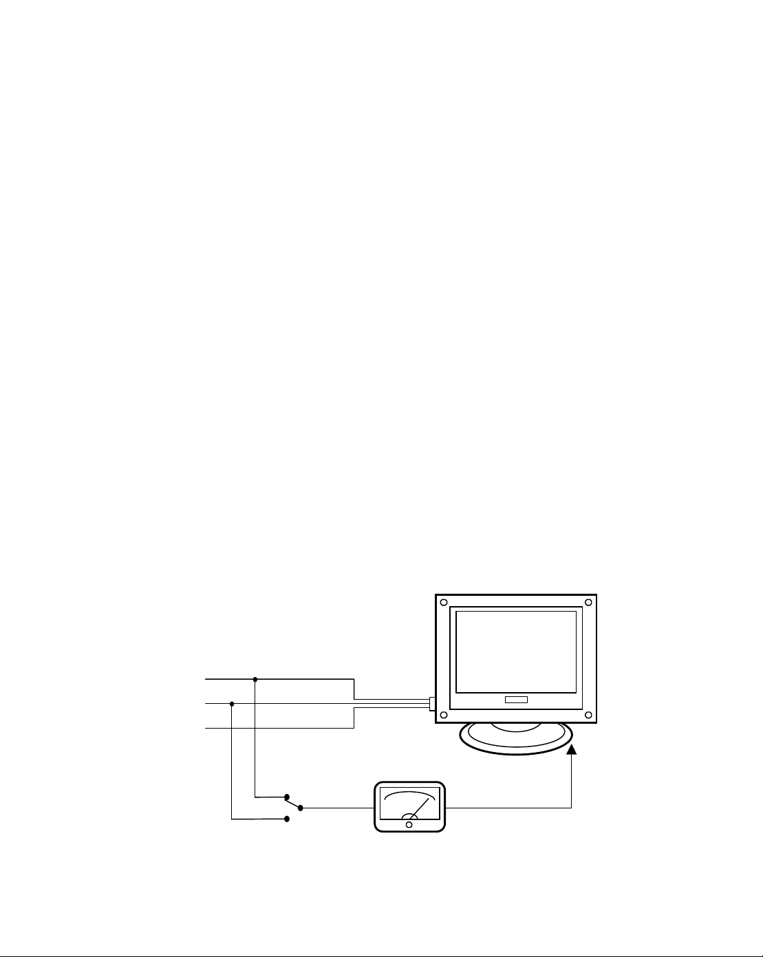
Connect the monitor power lead to the mains supply, via an isolation transformer, and switch on.
Using the test circuit shown in Fig.1-1, measure the AC leakage current between each pole ( L
and N) of the supply and all accessible metal parts. The earth leakage current must not exceed 3.5
mA.
L
Mains N
Input E
Connect to
Exposed Metal
Parts
Measuring Circuit
mA
Resistance=2000 ohms
Fig.1-1 AC Leakage Current Test Circuit
Page 4

1.2 Product Safety Notice
1) Many electrical and m echanical parts in this chassis provide special visual safet y protection.
The protection afforded by them cannot necessarily be obtained by using replacement
components rated for higher voltage, wattage, etc.
2) Before replacing any of these components, read the parts list in this manual carefully. The us e
of substitute replacement parts which do not have the same safety characteristics as
specified in the parts list may create shock, fire, X-Ray radiation or other hazards.
1.3 Service Notes
1) When replacing parts or circuit boards, wrap the wires around terminals before soldering.
2) When replacing a high wattage resistor (more than 1/2 W) on a circuit board, keep the resistor
about 10mm (1/2in.) away from circuit board.
3) Keep wires away from high voltage or high temperature components.
4) Keep wires in their original position so as to reduce interference.
Page 5
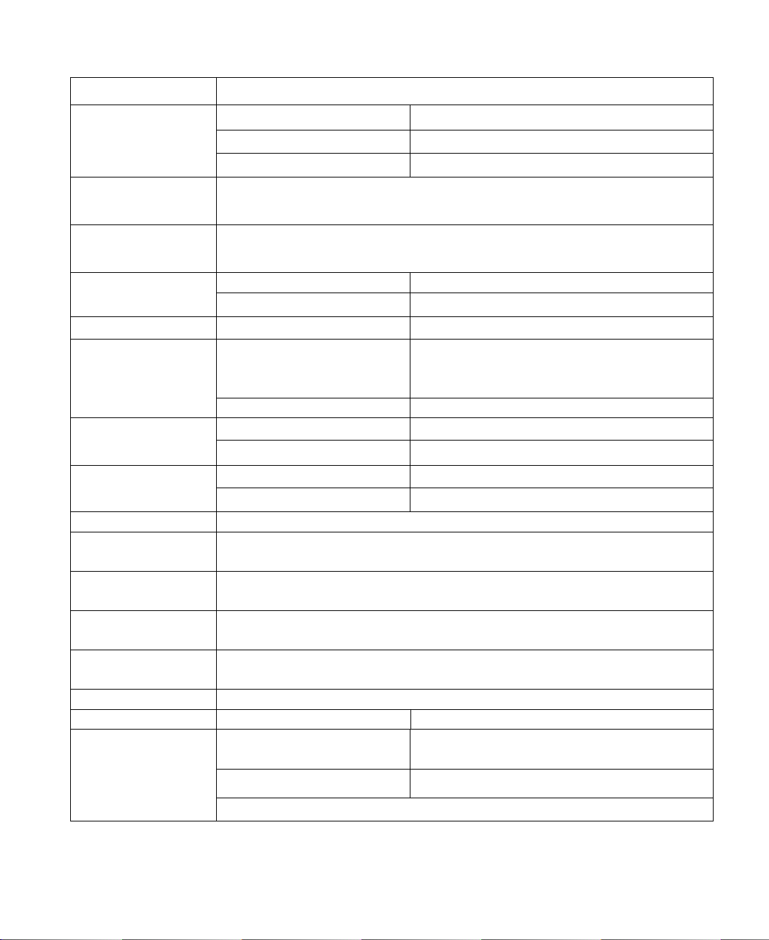
2. Specifications
2.1 Monitor Specification
Power Source
Power
Consumption
Picture Tube
Viewable Image
Size
Maximum
Resolution
Input Signals
Synchronization
Display Colours
Active Display
Area
Plug & Play
Operating
Temperature
Operating
Humidity
Storage
Temperature
Storage
Humidity
High Voltage
Dimension
Weight
AC 100 ~ 240V , 50 / 60Hz
LED color is green Normal Operation (Max.70W)
LED color is amber Stand By / Suspend Mode (Max.15W)
LED color is amber Off Mode (Max. 3W)
15" (Diagonal), glare, non- glare, anti-static, 90°Deflection,
0.28mm dot pitch, Low Radiation, Mini-Gun Tube.
13.9" (Diagonal)
Horizontal 1024 Pixels (Non-Interlaced)
Vertical 768 Lines (Non- Interlaced)
Video Analog 0.7 Vp-p / 75 ohm Positive
Separate Sync.
Horizontal 30KHz - 57KHz continuous
Vertical 50Hz - 120Hz continuous
Analog Input 16 million colours
Horizontal 260 mm
Vertical 195 mm
DDC1 / 2B
+5• ~ +35•
10 % ~ 80 % (Non-Condensing)
-20• ~ +65•
15 % ~ 80 %
25KV
Width 360 mm
Height
Depth 388 mm
TTL Level
Horizontal : Positive / Negative
Vertical : Positive / Negative
384 mm (With Base)
Height of Base : 58mm
11.3Kg (Net weight)/ 13.5Kg (Gross weight)
Page 6
2.2 Preset Timing Table(I) for HP
Mode Resolution H-Freq. V-Freq. Hs. pol. Vs. pol.
1
2
3
4
5
6
7
8
9
Preset Timing Table(II) for others
Mode Resolution H-Freq. V-Freq. Hs. pol. Vs. pol.
1
2
720 x 400 31.47 kHz 70.08 Hz Negative (-) Positive (+)
640 x 480 31.47 kHz 59.95 Hz Negative (-) Negative (-)
640 x 480 35.16 kHz 56.25 Hz Negative (+/-) Negative (+/-)
800 x 600 37.88 kHz 60.32 Hz Negative (+/-) Negative (+/-)
640 x 480 37.86 kHz 72.81 Hz Negative (+/-) Negative (+/-)
640 x 480 37.50 kHz 75.00 Hz Positive (-) Positive (-)
800 x 600 48.08 kHz 72.18 Hz Positive (+/-) Positive (+/-)
1024 x 768 48.36 kHz 60.00 Hz Negative (-) Negative (-)
800 x 600 53.67 kHz 85.00 Hz Positive (+) Positive (+)
720 x 400 31.47 kHz 70.08 Hz Negative (-) Positive (+)
640 x 480 31.47 kHz 59.95 Hz Negative (-) Negative (-)
3
4
5
6
7
8
640 x 480 37.50 kHz 75.00 Hz Negative (-) Negative (-)
640 x 480 43.30 kHz 85.00 Hz Negative (-) Negative (-)
800 x 600 46.88 kHz 75.00 Hz Positive (+) Positive (+)
800 x 600 53.67 kHz 85.00 Hz Positive (+) Positive (+)
1024 x 768 48.36 kHz 60.00 Hz Negative (-) Negative (-)
1024 x 768 56.47 kHz 70.00 Hz Negative (-) Negative (-)
Page 7
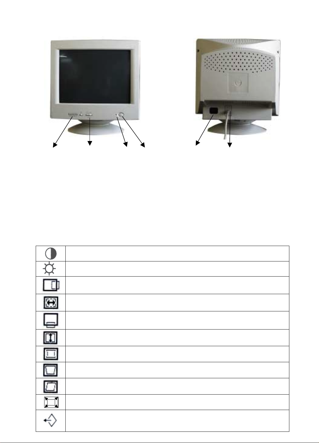
3. Control Location and Functions
Front View Rear View
1. 2. 3. 4. 1. 2.
1. Indication LEDs 1. AC Power Plug
2. Control Buttons 2. Signal Cable
3. Power Switch's LED
4. Power Sw itch
3.1 Indication LEDs :
When one of the digital controls is selected, the corresponding LED(s) are lit.
CONTRAST : To adjust the contrast of the display.
BRIGHTNESS : To adjust the brightness of the display.
H-POSITION : Adjust the horizontal position of the entire screen image.
H-WIDTH : Adjust the horizontal width of the entire screen image.
V-POSITION : Adjust the vertical position of the entire screen image.
V-HEIGHT : Adjust the vertical height of the entire screen image.
PINCUSHION : If the vertical sides of the screen image curve in or bulge out,
you can correct the pincushion distortion using this adjustment.
TRAPEZOID : If the picture is wider at the top or bottom, you can correct the
trapezoid distortion by using this adjustment.
P ARALLEL : If the sides of the screen image are tilted, you can use this
adjustment to correct the parallel distortion.
ZOOM : This is used to adjust H-width and V-Height, simultaneously.
RECALL : This is used to recall the original factory display settings.
Page 8

3.2 Control Buttons :
The Select Button (the left button) selects a digital control. The selected control is indicated by
the corresponding indication LED. The Down (down arrow) and UP (up arrow) buttons allow you to
decrease or increase the value of the selected control.
Press the Down (down arrow) and up (up arrow) simultaneously, Then it will degauss the
display.
3.3 Power Switch and LED
Push to power on the monitor and push again to power off. The indicator LED will be green
when the power switch is ON and the power cord is properly connected. The color of the LED
depends on the power state of the monitor. When the LED color is permanently green, it
indicates the monitor is at normal state. And when the power LED is amber, it indicates the monitor
is at a power saving state.
We recommend you switch on the monitor first, before switching on the computer!
Page 9
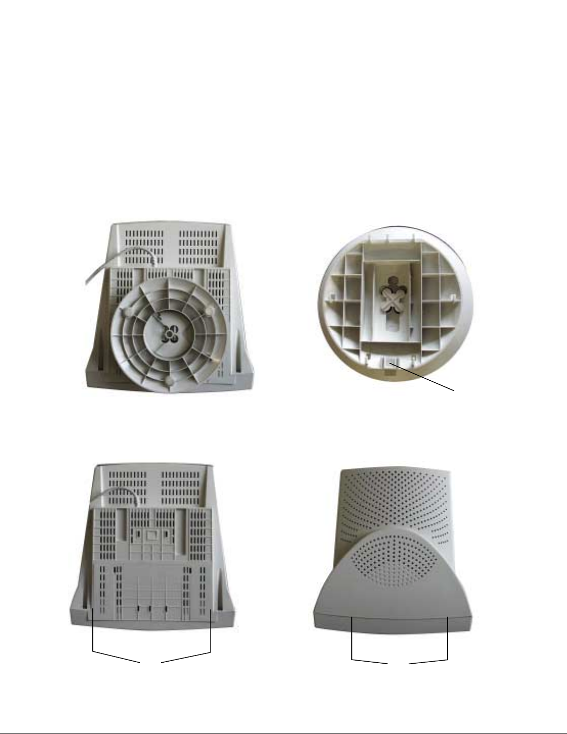
4. Disassembly Instructions
1) Face Down the Monitor : ( Fig.4-1 )
2) Swivel Base Removal : First press the stopper, then slide the swivel ball down and remove it.
( Fig.4-2 )
3) Back Cover Removal : Remove 4 screws (A) ( Fig.4-3 ) and (B) (Fig. 4-4) from the back cover.
Then remove the back cover.
4) PCB Assembly Removal :
CAUTION: When serving or replacing the CRT, disconnect the anode and discharge the anode
completely. As high voltage (25.0KV) may remain on the anode for an ex tended time after
power off.
( Fig.4-1 ) ( Fig.4-2 )
Stopper
(A) (B)
( Fig.4-3 ) ( Fig.4-4 )
Page 10
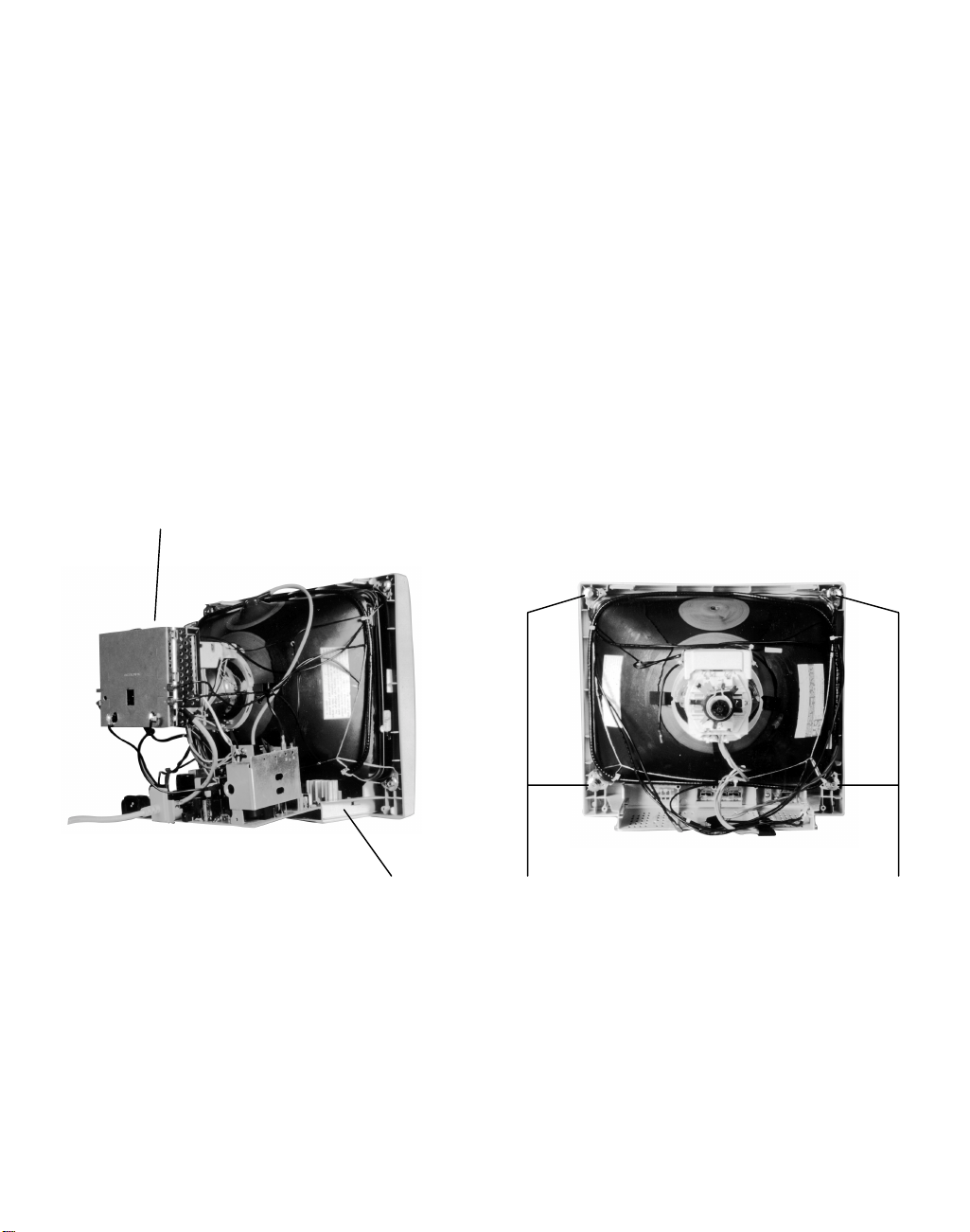
a) Unplug grounding connectors and the de gaussing coil grounding connector from the CRT
drive shield.
b) Remove CRT drive board (C) from CRT neck. (Fig.4-5)
c) Unplug the DY connector, AC connector, Degaussing coil connector and the CRT
grounding connector from the FBT shield.
d) Discharge the remaining static electricity by shorting CRT anode and ground, then remove
the FBT anode connector.
f) Press two clips(D) from left and right side of front cover(Fig.4-5) to remove main chassis.
5) CRT Removal :
CAUTION : Do not lift the CRT by the neck.
a) CRT is supplied as ITC.
b) Remove 4 screws (E) from the front cover (Fig.4-6) to move the CRT.
( Fig.4-5 ) ( Fig.4-6 )
Page 11
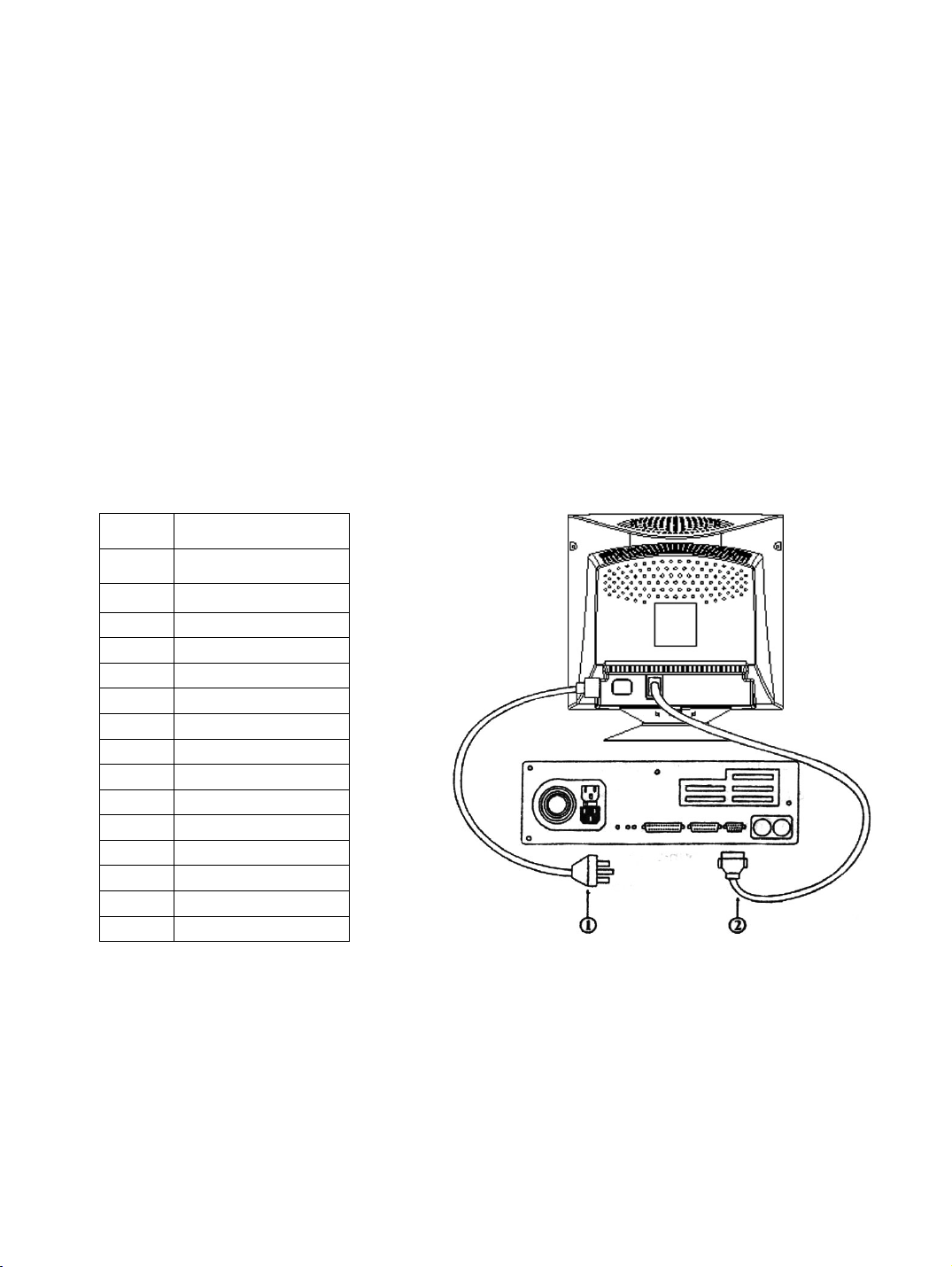
5. General Connection & Applications
Procedure for installing and using your Multi-Sync. display.
5.1 Connecting the monitor to the computer
1) Set up the display at the desired operation location , on top of or beside your personal computer .
Plug the power cord into the moni tor and t hen con nect the ot her end of th e power cord into an
AC outlet. The three-wire power cord is shielded type and is provided as a safety precautions to
ensure proper electrical grounding.
2) Connect the 15-pin color display shield signal cable to the video adapter output on your
computer, then lock both screws to ensure proper grounding. The connector information is as
follows :
PIN Description
1 Red
2 Green
3 Blue
4 Open
5 Return
6 Red Ground
7 Green Ground
8 Blue Ground
9 +5V ( PC97)
10 Ground
11 Open
12 SDA
13 H.Sync.
14 V.Sync.
15 SCL
3) First turn the PC power switch ON.Then apply power to the display by pressing the Power
ON/ OFF Switch to turn the monitor on. The power indicator LED will illuminate.
Allow about five seconds for the display tube to warm up, data will be displayed on screen.
NOTE : Don't force the cable into the connector; line it up carefully so that you don't bend the pins.
Page 12

6 . Electronic Circuit Description
6.1 Switching Mode Power Supply ( SMPS )
The switching mode power supply for this monitor is a full range type, i.e. universal power input
of AC 100V ~ 240V is compatible. When AC input is supplied through the slow blow fuse F801, the
line choke L803 to the rectifier D811 ~ D814, the rectified DC voltage is about 125V ~ 335V and then
fed to the switching transformer T801.
Prior to start, a small current flows to C808 via R828 and R831. I801 is to operate immediately
when the voltage across C808 reaches 16V. At the same time, Q801 is on, the rectified current flows
through the primary winding of T801 and the energy is stored in it .
When Q801 is off, the stored energy is transferred to the secondary winding, the auxiliary
winding is close-coupled and in phase with the secondary winding. It will provide a holding voltage
on C808 and fed to pin7 of I801 via R820 and D808. I801 will keep working provided that the voltage
across C808 is over 10V. The oscillating frequency of the switchin g mode power supply is around
20KHz, which is determined by the timing components R822 and C813. C813 is char g ed to 2.8V via
the 5V reference voltage at pin8 of I801and discharged to 1.2V during the discharged time interval.
The oscillator generates a series of blanking pulses, which cause the output at pin6 of I801 to go low.
The fly-back pulse from T403 is applied via D816 and R807 to force C813 to discharge, so that
the oscillating frequency is synchronized a nd kept in phase with tha t of horizontal fr equency to avoid
interference on display screen.
In case of voltage variations due to the change of input AC or output loading, the auxiliary
winding will reflect these variation to pin2 of I801 via D818, R812, R813, I803 and I802. The voltage
at pin2 of I801 is compared with the internal 2.5V reference voltage to produce an error voltage inside
I801.
This error voltage is limited to 1V by internal Zener diode and is compared with the voltage at
pin3 of I801 which is supplied from the voltage detected across R825 and R823, while Q801 is on.
Q801 is off only when the voltage drop across R825 and R823 has reached that of the error voltage, or
1 Vp-p maximum, that is, the duty cycle of the pulse width modulator is controlled by the combined
error voltage to regulate the output voltage.
Page 13
If over-load or short circuit occurs at the secondary, the voltage across R825 and R823 reaches
1Vp-p rapidly, thereby blocking the power output, the voltage at pin7 of I801 then decrease to below
10V, I801 is forced off.
However, in order to allow auto-recovery from power saving off state, the SMPS circuit is
designed as an unlatched type, the DC current flows via R828, R831, Q813 and D828 to charge C808
again. When the voltage across C808 has reached 16V, I801 is turned on again. Once the peak voltage
across R825 and R823 is over 1Vp-p, I801 will be forced off again. Consequently, I801 is turned on
and off repeatedly, under this situation, if the power does not be switched off, Q801, R825 and R823
may finally be over stressed and fail.
6.2 Power Management Circuit
Power
Switch
ON
OFF x x 1 0 OFF
I201
STATE
NORMAL 1 1 1 1 GREEN
STAND BY 1 0 0 1 AMBER
SUSPEND 0 1 0 1 AMBER
OFF 0 0 0 0 AMBER
I201 #40
(Vs)
I201 #39
(Hs)
I201 #29
(PM1)
I201 #28
(PM2)
D891 LED
When the display signal enters into "Stand By" or "Suspend" state of power saving, with either H.
Sync. or V. S ync. off, the voltage at pin29 of I201 is low, both Q808 and Q809 are switched off to
block the 16V voltage supply, thereby shut down the oscillation of the horizontal and vertical
deflection, power conservation is achieved.
When the display signal enters the "Off" state of power saving with both H. Sync. and V. S ync.
off, the voltage at pin28 and pin29 of I201 are low , then all Q805, Q806, Q808 and Q809 are switched
off. 1 1V and 16V voltage supply for the loading circuit are blocked. The overall power dissipation is
significantly reduced to less then 3W watt.
Automatic recovery from "Off" state to "NORMAL" state is achieved once the recovery H. Sync.
and V. Sync. trigger I201 via R254 and R256, the voltage at pin28 and 29 of I 201 will go high again to
turn on Q809, Q806 via Q808 and Q805.
Power Indicator
The power indicator D891 is composed of two LED in one. The 5V voltage is applied through
R244 to lighten the Green LED and through R243 to lighten the Yellow LED of D891. D891 is
controlled by the power management voltage, result in Green or Amber color for Normal or Stand By ,
Suspend, Off State respectively.
Page 14

Heater Voltage
The heater element in the CRT is supplied with 6.3±0.3V during normal operation and reduced
to 5.0±0.5V during Stand By or Suspend state. To achieve this, Q805, Q806 and associated circuit is
introduced, when at normal state, PM2 is HIGH level then Q805 ON, to trigger Q806 ON, 10V from
D815 to Q806, R841, R991 and heater, the heater voltage is 6.3V±0.3V.
When at Suspend, Stand-By state the horizontal output is shut down, there is no horizontal pulse,
PM1 is Low level, the feedback voltage at pin2 of I801 is higher than that of normal state. This will
force the output voltage at secondary side of T801 drop down, the heater voltage is reduced to 5.0±
0.5V .
6.3 Automatic Degaussing Circuit
The posistor R803 and the degaussing coil L891 comprise an automatic degaussing circuit to
demagnetize the shadow mask and the interna l shield of the CR T in order to pr otect the display screen
from color impurity.
The resistance value of the posistor is originally low (7 ohm) during power off. Right after the
display is powered-on, the voltage at pin26 of I201 is HIGH, then Q803 ON and RL01 triggered a
large AC current flows through the posistor into the degaussing coil for demagnetization.
Meanwhile, the resistance of the posistor increase rapidly due to rising of its temperature, the
degaussing current thus decreases to less then 100mAp-p in a few seconds so that display screen
settles quickly, degaussing function is then complete. After 5 seconds, the voltage at pin26 of I201 is
LOW, then Q803 OFF and RL01 release.
6.4 Micro Control Circuit
MTV212AN32 / MTV212AN64
The monitor uses an advanced CPU I201 to control the Contrast, Brightness, H. Position, H.
Width, V. Position, V. Height, Pincushion, Trapezoid and Parallelogram, Zoom, Recall.
The horizontal sync. and vertical sync. are via R254, R256 then fed to pin39, pin40 of I201. The
output sync signals are fed to pin1 and pin2 of deflection processor I401 via pin33, pin32 of I201.
The control signals on pin1, pin2 are for PWM (Pulse Width Modulation) which are converted
into DC voltages via integration circuits. With the Brightness control signal as an example, the PWM
control signal is derived from pin2 of I501 which is fed into a integration circuit R209, C202
Page 15

and pull-up resistor R208. The other control function is by I2C-bus, the SCL and SDA signals are fed
to pin30 and pin31 of deflection processor I401 via pin10 pin9 of I201.
The CPU is reset by the components C204, C203 and D213 at pin4 of I201, when the AC source
is connecting, every time to ensure correct start.
The +5 voltage is fed into I201 via pin5, a 12MHz resonator (o r crystal) is connected at pin7,
pin8 of I201 to generate the CPU clock for the software execution. The user key control input is fed to
the A/D converter at pin22, pin23 via R229, R231, R257,R258 and S201•S202.
The function indictors are connected to pin16 ~ 21 of I201. The control signal for horiz ontal
linearity circuit is derived from pin14 of I201 which is fed to the CS circuit Q425, Q424.
There is a low power override pin on pin15 of I201, this pin is connected to pin12 of the signal
cable P501. When the signal cable is disconnected from the computer, this pin is h igh, and the power
saving function will be disable. Meanwhile, the CPU I201 will activate the self-test signal from pin1 1
to generate a Self-Test Pattern. When the signal cable is connected to the compu ter, this pin is
low and the power saving function will be enable, the CPU can generate a power saving signal control
voltage at pin29 and pin28 of I201. Note that, the Self-Test Pattern will not appear once the signal
cable is connected to the computer.
The monitor is design to have the DDC 1/2B functions, communication between the monitor and
computer for DDC is via pins24, 25 of I201 which are defined as SDA, SCL signals. The computer
will read out the EDID data from the EEPROM I202 via I2C data lines. The EDID data is written into
the EEPROM in the factory during production. The memory size for EDID data is 128 bytes
which is shared from EEPROM 1202 which has 4K bytes memory size.
6.5 How to enter into the factory setting ?
The monitor includes 9 factory preset timings for HP, or 8 factory preset timings for others, the
preset mode timing detect by the Mcu I201 Pin.37. although only some of the timing are fine tuned by
auto alignment during production.
Switch off the monitor, push and hold down the Select control key , power on again, wait 1.0
second then release the Select ke y, the monitor should now be in the fact ory setting mode, all the
LEDs will now be illuminated. Selection of function will be indicated by the extinguishing of the
appropriate LEDs, All adjustment data will be stored automatic ally, then power on again, the monitor
will reverse to normal operating state.
Page 16

6.6 Deflection Processor
6.6.1 I401 is used for S1D2511B
I401 S1D2511B is a Samsung monolithic integrated circuit assembled in a 32 pins shrunk dual
in line plastic package. I 401 controls a ll the f unctions re late d to the horizon t al a nd ve rtica l def lec tion
in a multi-sync monitor. All functions are controllable by I2C-bus.
6.6.2 Pin-Out Description for S1D2511B ( I401 )
PIN SYMBOL DESCRIPTION
1 H/HVIN TTL compatible horizontal sync input (Separate or composite)
2 VSYNCIN TTL compatible vertical sync input (for separated H&V)
3 HLOCKOUT First PLL lock/ unlock output (0V unlocked, 5V locked)
4 PLL2C Second PLL loop filter
5 C0 Horizontal oscillator capacitor
6 R0 Horizontal oscillator resistor
7 PLL1F First PLL loop filter
8 HPOSITION Horizontal position filter (Capacitor to be connected to HGND)
9 HFOCUSCAP Horizontal dynamic focus oscillator capacitor
10 FOCUSOUT Mixed horizontal and vertical dynamic focus output
11 HGND Horizontal Section Ground
12 HFLY Horizontal flyback Input (positive polarity)
13 HREF Horizontal Section Reference Voltage (to be filtered)
14 COMP B+ error amplifier output for frequency compensation and gain setting
15 REGIN Regulation input of B+ control loop
16 ISENSE
17 B+GND Ground (related to B+ reference adjustment)
18 BREATH
19 VGND Vertical section ground
20 VAGCCAP
21 VREF Vertical section reference voltage (to be filtered)
22 VCAP Vertical sawtooth generator capacitor
23 VOUT
24 EWOUT Pincushion-East/ West correction parabola output
25 XRAY X-RAY protection input (with internal latch function)
26 HOUT Horizontal drive output (internal transistor, open collector)
27 GND General ground (referenced to Vcc)
28 BOUT B+ PWM regulator output
29 Vcc Supply voltage (12V typ)
30 SCL I2C clock input
31 SDA I2C data input
32 5V Supply voltage (5V typ)
Sensing of external B+ switching transistor current or switch for
step-down converter
DC breathing input control (Compensation of vertical amplifier against
EHV variation)
Memory capacitor for automatic gain control loop in vertical ramp
generator
Vertical ramp output (with frequency independent amplitude and S or C
corrections if any). It is mixed with vertical position voltage and vertical
moire
Page 17

6.7 Vertical Deflection Circuit
The power amplifier drive the vertical yoke asse mbly is a DC design based on power amplifier
I301 TDA8172.
The TDA8172 consists of a differential input stage, two power supply (+10V and –11V), a
flyback generator, a protection circuit for the output stages. The differential input stage has a high
CMRR differential current mode input (pin6 and pin7 ). This differential sawtooth signal is derived
from pin21, 23 of I401.
The flyback voltage will be generated internally by doubling the supply voltage and therefore a
separate flyback supply voltage is not needed.
The Vout (pin 5) provides a blanking signal for the CRT via D302, R301, R302.
6.8 Horizontal Deflection Circuit
The product designed around a base-drive circuit driving horizontal deflection circuit to provide
sufficient switching current. Q401 is switched by the horizontal drive signal from pin8 of I401 via
R427, C475. This produces a sufficient voltage to T401, snubber network R448, C410 compensates
for leakage inductance in T401 and shapes the base drive waveform.
The drive signal is fed to Q403 via D431,R431, R430. When Q403 is at the "Off" state, the
voltage which is stored on the base of Q403 discharge via R431, D431. The drive signal control Q403
switch on-off, so that saw-tooth waveform current flows in the horizontal deflection coil is obtained.
The positive horizontal fly-back pulse signal derived from pin6 of T403 is fed to pin1 of I 401 via
R411, this fly-back signal provides proper timing reference for horizontal drive output.
The horizontal deflection output circuit combine the transistor switching function with a
damping diode to generate saw-tooth waveform current flow through the deflection coil.
The basic horizontal deflection output circuit comprises switching transistor Q403, fly-back
transformer T403 , damper diode which included D413, D414 tuning capacitor C413, modulation
capacitor C414, S-shape correction capacitor C415 / C452 and linearity coil L402.
Page 18

When the horizontal frequency of input signal is greater then 42.4KHz, Q425 is on, Q424 is off,
C415 is the only capacitor for S-shape correction.
Input H.
Frequency
Fh < 42.4KHz 0 ON ON
42.4KHz < Fh 1 ON OFF
I201#17 Cs C415 C452
6.9 Horizontal Width Control
The monitor uses a diode modulation circuit for the control of horizontal width, it is achieved by
changing the base voltage of Q418, the control voltage (0~ 5V ) is from pin11 of I401 via R454,
which consist of horizontal pincushion & corner correction & DC shift & trapezium correction. There
are controlled by I2C-bus via I201, low DC shift voltage will cause large width control current flows
out pin11 of I401 via R454 and then the horizontal width is increased.
6.10 Pincushion and Trapezoid Control
The combined pincushion and trapezoid control signal output from pin11 of I401 is applied to
the base of Q418 via R454. This parabolic signal modulates the horizontal width automatically. So
that dynamic pincushion correction ( DPC ) and trapezoid distortion correction are achieved .
6.1 1 Spot Killer Circuit
The spot killer circuit is included, in order to prevent CRT from spot damage while switching
power on or off. -160V derived from pin7 of T403 is applied via D449, R490, R487 to collector of
Q406. When power is off, -160V is fed to G1 via R490 and R488 to cut off the beam current.
On particular occasion, when X-ray protection is activated, pin17 of I401 go high, then Q402 is
turn-off, Q406 turn-off, -160V is fed to G1 via R490 , R488 to cut off the beam current.
6.12 Brightness Control Circuit
The brightness control voltage derived from pin2 of I201 is applied via R209, R407 to control
the bias of Q402 and Q406, G1 voltage is changed accordingly to obtain desired screen brightness.
6.13 Blanking Circ uit
The vertical blanking pulse derived from pin5 of I301 and pin14 of I401 are applied via D302
and D301 respectively and combined together through R303 to cut off Q402, Q406. This blanking
signal is fed to G1 via R490, R488 to prevent retrace lines from appearing on the display screen.
Page 19

6.14 H.V. Control Circuit
The horizontal feedback signal derived from pin6 of T403 is applied via D403, R415, R420,
R402, R416 and peak-detected by C474 and R492, then fed to the error amplifier on pin5 of I401, the
value of R410 is chosen to have a suitable gain for the error amplifier.
The saw-tooth waveform signal related to the out put current of Q413 is fed to pin4 of I401 via
R451 for current mode regulation.
Both of the horizontal feedback signal and saw-tooth waveform signal are fed to a comparator in
I401 to generate a PWM ( Pulse Width Modulation ) control signal at pin6 of I401 , this square
waveform control signal is then fed to Q413 via b uffer Q412. Q413 is designed as a step -up volta ge
converter, the DC voltage is fed to the Drain of Q413 via L417, the energy is stored in L417 when
Q413 is on , and released when Q413 is off.
The circuit supplies DC voltage ( 90V ~ 190V ) to pin9 of T403 for horizontal scanning via
Q413 and D440, this supply voltage is approximately proportion to the horizontal frequency in order
to keep the scanning amplitude constant when the horiz ontal frequency changes. The snub circuit
consists of C442, R442, R441, C441 is for noise limitation.
Page 20

6.15 Video Circuit
The analog R. G. B. video input signals are supplied through the cable which is terminated at
P501, these input signals are approximately 0.7 Vp-p in amplitude.
R501/ R531/ R561 give a resistance of 75 ohm for impedance matching. The R. G. B. video
signals are AC coupled via C501/ C531/ C561 then fed into the video pre-amplifier I501 at pin6, pin3
and pin1 respectively.
R503/ R533/ R563 act as R. G. B. video gain control. DC bias to the video gain controls are
through R502/ R532/ R562 which are connected to 12V voltage.
After being pre-amplified, the R. G. B. video signal are output from pin14, pin17, pin20 of I501
respectively. Signal amplitude at these output are about 3 ~ 4 V p-p.
The DC contrast control voltage from R584 is applied to pin9 of I501 which varies the AC gain
of all three R. G. B. channel amplifiers simultaneously. C582 added at pin9 of I501 to prevent noise
entering into the IC.
The video output amplifiers are composed of typical cascode stages. Q901/ Q902, Q931/ Q932,
Q961/ Q962 amplify the video signals to amplitude level of about 35 ~ 45 Vp-p, which is enough to
drive the CRT cathodes. The feedback emitter resistors R901/ R902, R931/ R932, Q961/ Q962 and
the emitter peaking capacitors C902/ C932/ C962, the peaking coils L901/ L902, L931/ L932, L961/
L962 are for frequency response compensation.
The cathode cut off voltage settings required for white balance are achieved by adjusting R910/
R940 / R970.
The series surge limiting resistors R908/ R938/R968 for the video amplifiers will form a
low-pass-filter with the CRT capacitance, therefore offering protection against flash-over.
Page 21

7. Adjustment PCB Main Parts Location
MAIN BOARD ( Component Side View) PWB-0248
S202 D891 S201 D206..............D201
R420
D201~
D206—Display LED's
D891—Power LED
R420—H.V. Adjust
R471—ABL Adjust
S202—Power Switch
S202—
—
—
T403—FBT
Up Button
•
Down Button
•
Select Button
T403
R471 T403
CRT DRIVE BOARD ( Component Side View )
PWB-0239
R563
r903
R970
R910
R940
FOCUS
SCREEN
R533
R503—R. Drive R910—R. Cut off
R533—G. Drive R940—G. Cut off
R563—B. Drive R970—B. Cut off
SCREEN—G2
Page 22

7.3 High Voltage Adjustment
a ) Apply a Super VGA signal ( 54KHz ) with crosshatch pattern.
b ) Set the BRIGHTNESS control to 0.06FL and CONTRAST control to maximum.
c ) Adjust H.V. Adj. R420 for the high voltage to be 25.0KV±0.2KV.
7.4 Auto Sizing Adjustment
To enter into the factory setting mode, operate according the following procedure:
Switch off the monitor first, push and hold the SELECT Button, power on again, wait 1.0 second
then release the SELECT Button, the monitor is now in the factory setting mode, the lighting of the
LED's will reverse and all the data of adjustment will be stored in the factory setting automatically.
a ) Ensure completion of the H.V. Adjustment before starting the presets.
b ) Setup the timing table in your pattern generator.
c ) Adjust the Trapezoid and Pincushion control to the optimized position for each mode.
d ) Adjust the H. Position, H. Width, V. Position and V. Height to the optimized position for each
mode according to the specification.
e ) Switch off the power, then switch on again. The monitor will revert to its normal state.
7.5 White Point Adjustment
a ) Apply 54KHz signal with background pattern .
b ) Set the BRIGHTNESS and CONTRAST control keys to maximum.
c ) Preset R910 , R940 and R970 to the center position.
d ) Use a photo meter and adjust the G2 VR on T403 to set screen center brightness to 0.8FL.
e ) Use a color analyzer to set the color coordinate to x = 0.281, y = 0.281 by adjusting the R. cut -off
control R910 and G. cut-off control R940.
f ) The background brightness should be 0.7 FL ~ 0.9 FL.
g ) Set the BRIGHTNESS to the 0.06FL and the CONTRAST to maximum.
h ) Apply a 50 ×50mm green square pattern to the unit.
i ) Adjust G. gain control R533 to set the central brightness to be 33FL.
j ) Apply a 50 ×50mm white square pattern to the unit.
k ) Use a color anal yzer to set the color coordinate to x = 0.281, y = 0.311 by adjusting the B. gain
control R563 and R. gain control R503.
Page 23

7.6 Focus Adjustment
a ) Apply a 54KHz signal with crosshatch pattern.
b ) Adjust FOCUS control on T403 to get the best overall focus.
7.7 Convergence Adjustment
Note 1: For a unit with new ITC, adjustment for convergence may not be necessary.
2 : Prior to alignment procedures must be completed.
a ) Apply a VGA signal with background pattern to the unit.
b ) Set BRIGHTNESS control to 0.06FL.
c ) Apply a VGA signal with full-white pattern to the unit.
d ) Use a photo meter to set the screen center brightness up to 20 FL by adjusting the CONTRAST
control.
e ) Apply a VGA signal with crosshatch pattern to the unit.
f ) Loosen the convergence magnet ring with a screw driver.
g ) Converge the red and blue lines at the center of screen by rotation the two tabs of the 4 poles
static convergence magnet.
h ) Tighten the convergence magnet lock with a screw driver.
Page 24

8. Troubleshooting Flow Chart
(1) Power Start NG
Is
No the voltage
at C804 normal
(125-340V)
?
Is Yes
F801 open Yes
?
Power start NG
No R808 open
?
Check power socket copper
No
and plug & D811•D814,
R804
Are
the start-up
No voltage at C808>16V
and Operation Voltage at
C808 > 10V
?
Check R828, R831, R856,
Yes
R857, R859, Q813, D828,
D808, R820, Q812.
Yes
No
Is
The voltage
Of C815 Normal
(> 1Vpp)
Check Q804, I803, Q815.
Is Yes
Check Q801, I801
Check secondary side circuit
D805, D815•D819, R821 or any
short circuit (Q413, Q403, I301) .
Page 25

(2) No Data Appear
No data appear
Are
No the waveforms
at pin 1,3,6 of I501
normal
Check signal cable &
?
C501, C531, C561
Yes
Are the
voltages at pin 13 No
of I501 normal
?
Check R471, D451, D404, I402,
D401, R405, R404, R584.
Yes
Are
the waveforms
at pin 14, 17, 20,
of I501 normal No
?
Is the
Yes voltage at pin 8 & Yes
19 of I501 normal
?
Are
No the waveforms
at cathode R/G/B of
Check video circuit
CRT normal No
Q901,Q931,Q961,
?
Q902,Q932,Q962 .
Yes
Check 8V lines .
No
Check 75V lines .
CRT is defective
Check D503, R509
I501 is defective
Page 26

,
No raster appear
(3) No Raster Appear
Is the Yes
H.V. correct
?
Is
No the voltage Yes
Yes Is at heater normal
Check Q403, Q413.
Q403, Q413 (6.3V)
short? ?
No No
Check R841,
R991, CRT
Socket
Is the
No voltage at pin
Check DC to DC
9 of T403 normal
control circuit
(80-190V)
D440, C439, L417,
? No
R443, R451.
Yes
DD Is Is
the waveform the waveform Yes
at base of Q403 at pin 8 of I401
normal normal
? ?
Check I401
Yes No
Check brightness
circuit, Q402, Q406.
Check spot killer
circuit:
D302, D422.
Check FBT, CRT.
Check Q401,
R431, C475,
R427, R468,
D453
Is the
voltage at C409
normal ? Yes
No Is the No
Is the voltage at G1
Yes H.V. protection normal ?
Circuit active
Check R415, R402,
? Yes
R420, R406, R416,
No
R414.
Check C409, D403,
R413
R414, C407
Check CRT.
Page 27

4
(4) R/G/B is Missing
R/G/B is Missing
(5) Loss of Vertical Synchronization
Loss of vertical
synchronization
at pin 1, 3, 6 of
I501 normal
Is the
waveform No Is the
Check signal cable
C501, C531, C561
waveform at Yes
pin 32 of I201
? normal ?
the waveform No
Yes No
Is
I501 is defective
at pin 14, 17, 20 of
I501 normal
?
Yes Is the
waveform at No pin 40 of I201
KR/KG/KB of CRT normal ?
normal ?
Yes
CRT is defective
Is the waveform at No
Check video circuit
Q901, Q931, Q961
I201 is defective
Q902, Q932, Q962
Check 8V lines,
Check 75V lines.
Check I401, R32
C301, R323, C30
Check R256.
Yes
Page 28

Loss of horizontal
synchronization
No vertical scanning
(6) Loss of Horizontal Synchronization (7) No Vertical Scanning (One Horizontal Line)
Is the Is the
waveform at Yes waveform at Yes
pin 33 of I201 pin 5 of I301
normal ? normal ?
No No
Check I401, R423,
R433,
R434, C412, R42
C454, C406.
Deflection yoke is
defective
Are the
No voltages of I301 Yes
at pin 1•10V and
pin 4 •–10V
?
Yes
waveform at No Are the
pin39 of I201 waveforms at Yes
normal ? pins 6,7 of I301
Yes
No
Are
Is the
I201 is defective Check R254.
normal ?
Q806 or I301 defective
I301 is defective
the waveforms Yes
at pin 12,13 of I401
normal ?
No
I401 is defective
Check R322, R323
Page 29

Micro Control Abnormal
(8) Micro Control Function
Is the Yes
function LED
working ?
Press UP
No or DOWN key, Yes
can it adjustment
?
No
Check R230, R231,
R257, S202.
Check S201 – S202.
I202 is defective.
H. Size Abnormal
(9) Horizontal Width Control Abnormal
Is H.size No
control function
working
? Is
the voltage at No
Yes the base of Q418
normal ?
Check I402.
Check Q416-Q419, L415.
Check pin11 of I401.
Page 30

9. BLOCK DIAGRAM
11V
75V
100V• 16V
240V
Vac
L803,
D811•D814
EMI Filter
Rectifier
I/P
V901 CRT
Pulse G1 G2
From 12V
FBT
T403
Q805, Q806,
Q808, Q809
Power Saving
Contrast
5V 11V
V. V.
V.
H.
R256
R254
Sync.
Buffer
H. H.
SCL/ SDA DDC
Key Control
S201•S202
I201
MCU Control
Self Test
H/V Center
H/V Size
DPC
Trapezoid
CS Control
Brightness
Contrast
LED
I 801
T801 D815
Q801 D819
D808 D817
Q812 D818
Q828 D805
Q815
SMPS
Q807
R806
D802
D891
Power
LED
Q804
D825
I202
EEPROM
R413,
R414, C407
X Ray
Protection
Q412, L417, D440
I401
H./V.
Deflection
Controller
DC-DC HV Adj.
Control
V. O/P
H. O/P
X Ray DPC O/P
I402
H-Size
R991 6.3V Heater
R R KR
G G KG
B B KB
I501
Video
Pre-Amp.
Q901, Q902
R. Video Output
Q931, Q932
G. Video Output
Q961, Q962
B. Video Output
PWB-0239
D422, D409, D302,
D301 Blanking.
Q402, Q406
Brightness
I301
Ver. Output
Q403, D413, C413
Hor. Output
L415
C414
C457
Diode
Mod.
Q424
Q425
CS
Control
R420
HV Adj.
Q401, T401
Driver
Q417, Q418
Q416, Q419
Width Adj.
DPC Amp.
Trapezoid
Focus Anode
Ver. D.Y.
Hor. D.Y.
C404, T402
Dynamic
Focus
T403
FBT
PWB-0248
D201-D206
Function LED
DC-DC Converter
28
Page 31

12. Electrical Parts List
WARNING : Replacement parts which have special characteristics important to safety should be replaced
only with types identical to those in the original circuit or specified in the parts list. Before
replacing any of these components, read carefully the product safety precautions. Do not
degrade the safety of the display through improper servicing.
ASSEMBLY PCB-MAIN (PWB-0248)
Ckt No. Part No. Description Specification Remarks
C201 5213647991 CAPACITOR, ELECTROLYTIC 50V 4.70UF M
C202 5213647991 CAPACITOR, ELECTROLYTIC 50V 4.70UF M
C204 5231310391 CAPACITOR, CERAMIC 50V 10000.00PF K
C205 5213322191 CAPACITOR, ELECTR OLYTIC 16V 220.00UF M
C206 5213610091 CAPACITOR, ELECTR OLYTIC 50V 10. 00UF M
C208 5236310491 CAPACITOR, BARRIER LAYER 50V 0.10UF Z
C209 5236310491 CAPACITOR, BARRIER LAYER 50V 0.10UF Z
C210 5242239091 CAPACITOR, CERAMIC 50V 39.00PF J
C211 5242215191 CAPACITOR, CERAMIC 50V 150.00PF J
C212 5242215191 CAPACITOR, CERAMIC 50V 150.00PF J
C215 5236310491 CAPACITOR, BARRIER LAYER 50V 0.10UF Z
C216 5236310491 CAPACITOR, BARRIER LAYER 50V 0.10UF Z
C221 5242282091 CAPACITOR, CERAMIC 50V 82.00PF J
C222 5242282091 CAPACITOR, CERAMI C 50V 82.00PF J
C301 5231322291 CAPACITOR, CERAMIC 50V 2200.00PF K
C303 5275133491 CAPACITOR, METALLIZ ED 63V 0.33MF J
C304 5236310491 CAPACITOR, BARRIE R LAYER 50V 0.10UF Z
C305 5275147491 CAPACITOR, METALLIZED 63V 0.47MF J
C321 5205310212 CAPACITOR, ELECTR OLYTIC 16V 1000. 00UF M*10X20
C322 52133471 12 CAPACITOR, ELECTROLYTIC 16V 470.00UF M
C323 5271 110491 CAPACITOR, METALLI ZED 100V 0.10UF J
C324 5205610191 CAPACITOR, ELECTR OLYTIC 50V 100. 00UF M *
C325 5222447391 CAPACITOR, POLYESTE R 100V 47000.00PF J
C401 5231310291 CAPACITOR, CERAMI C 50V 1000.00PF K
C402 5213601091 CAPACITOR, ELECTR OLYTIC 50V 1. 00UF M
C403 5236310491 CAPACITOR, BARRIE R LAYER 50V 0.10UF Z
C404 5223468301 CAPACITOR, POLYPROP YLELE 250V 68000.00PF J
C405 5236310491 CAPACITOR, BARRIE R LAYER 50V 0.10UF Z
C406 5222410291 CAPACITOR, POLYESTE R 100V 1000.00PF J
C407 5213322091 CAPACITOR, ELECTR OLYTIC 16V 22. 00UF M
C408 5213647991 CAPACITOR, ELECTR OLYTIC 50V 4. 70UF M
C409 5213647991 CAPACITOR, ELECTR OLYTIC 50V 4.70UF M
C410 5231333291 CAPACITOR, CERAMI C 50V 3300.00PF K
C411 5213610191 CAPACITOR, ELECTROLYTIC 50V 100.00UF M
C412 5213422091 CAPACITOR, ELECTROLYTIC 25V 22.00UF M
C413 5223739201 CAPACITOR, POLYPROPYLELE 1600V 3900.00PF J
C413A 5056208100 EYEL ET 1.6x3.0 1.6x3.0x2
C414 5223647201 CAPACITOR, POLYPROP YLELE 630V 4700.00PF J
C415 5270447402 CAPACITOR, METALLIZED 400V 0.47UF J
C416 5242218191 CAPACITOR, CERAMI C 50V 150.00PF J
45
Page 32

C422 5231322291 CAPACITOR, CERAMIC 50V 2200.00PF K
C423 5213610091 CAPACITOR, ELECTROLYTIC 50V 10.00UF M
C424 5236310491 CAPACITOR, BARRIER LAYER 50V 0.10UF Z
C428 5236310491 CAPACITOR, BARRIER LAYER 50V 0.10UF Z
C429 5236310491 CAPACITOR, BARRIE R LAYER 50V 0.10UF Z
C432 5213447091 CAPACITOR, ELECTR OLYTIC 25V 47. 00UF M
C434 5213601091 CAPACITOR, ELECTR OLYTIC 50V 1. 00UF M
C439 5213622991 CAPACITOR, ELECTR OLYTIC 50V 2. 20UF M
C441 5233327191 CAPACITOR, CERAMI C 1KV 270.00PF K
C442 5232322191 CAPACITOR, CERAMI C 500V 220.00PF K
C443 5214347012 CAPACITOR, ELECTR OLYTIC 200V 47. 00UF M
C444 5214347012 CAPACITOR, ELECTROLYTIC 200V 47.00UF M
C446 5213601091 CAPACITOR, ELECTROLYTIC 50V 1.00UF M
C452 5270364401 CAPACITOR, METALLIZED 250V 0.64MF J
C452A 5056208100 EYEL ET 1.6x3.0 1.6x3.0x2
C454 5275122391 CAPACITOR, METALLIZED 63V 22000.00PF J
C457 5271 122502 CAPACITOR, ME TALLIZE D 100V 2.20UF J
C459 5231310291 CAPACITOR, CERAMIC 50V 1000.00PF K
C464 5214410012 CAPACITOR, ELECTROLYTIC 250V 10.00UF M
C465 5242218191 CAPACITOR, CERAMIC 50V 150.00PF J
C468 5236310491 CAPACITOR, BARRIER LAYER 50V 0.10UF Z
C475 5213422091 CAPACITOR, ELECTROLYTIC 25V 22.00UF M
C480 5276110491 CAPACITOR, METALLIZED 100V 0.10UF J
C489 5232347191 CAPACITOR, CERAMI C 500V 470.00PF K (Optional)
C801 RA 5230105001 CAPACITOR, CERAMI C 400V 4700.00PF M
C801 RB 5230105501 CAPACITOR, CERAMIC 400V 4700.00PF M
C802 RA 5230105001 CAPACITOR, CERAMI C 400V 4700.00PF M
C802 RB 5230105501 CAPACITOR, CERAMIC 400V 4700.00PF M
C803 5231310291 CAPACITOR, CERAMIC 50V 1000.00PF K
C804 5210313400 CAPACITOR, ELECTROLYTIC 400V 220.00UF M
C804A 5056208101 EYEL ET 2.4x3.0 2.4x3.0x2
C805 RA 5270106301 CAPACITOR, METALLIZED 250V 0.47UF M
C805 RB 5270108101 CAPACITOR, METALLI ZED 250V 0.47UF M
C806 5233310301 CAPACITOR, CERAMIC 1KV 10000.00PF K
C808 5213410191 CAPACITOR, ELECTROLYTIC 25V 100.00UF M
C809 5213610091 CAPACITOR, ELECTROLYTIC 50V 10.00UF M
C810 5236310491 CAPACITOR, BARRIER LAYER 50V 0.10UF Z
C811 5231322291 CAPACITOR, CERAMIC 50V 2200.00PF K
C812 5213347112 CAPACITOR, ELECTROLYTIC 16V 470.00UF M
C813 5221 110391 CAPACITOR, POLYESTER 50V 10000.00P F J
C814 5248468091 CAPACITOR, CERAMIC 2KV 68.00PF K
C815 5231347191 CAPACITOR, CERAMIC 50V 470.00PF K
C817 5213622991 CAPACITOR, ELECTROLYTIC 50V 2.20UF M
C818 5214101091 CAPACITOR, ELECTROLYTIC 100V 1.00UF M
C819 5213347091 CAPACITOR, ELECTROLYTIC 16V 47.00UF M
C820 5213410191 CAPACITOR, ELECTR OLYTIC 25V 100.00UF M
C821 5234333191 CAPACITOR, CERAMIC 2KV 330.00PF K
45
Page 33

C828 RA 5270106201 CAPACITOR, METALLIZ ED 250V 0.22MF M
C828 RB 5270109501 CAPACITOR, METALLI ZED 275V 0.22MF K
C830 RA 5230105001 CAPACITOR, CERAMI C 400V 4700.00PF M
C830 RB 5230105501 CAPACITOR, CERAMIC 400V 4700.00PF M
C831 RA 5230105001 CAPACITOR, CERAMI C 400V 4700.00PF M
C831 RB 5230105501 CAPACITOR, CERAMIC 400V 4700.00PF M
C832 5232310191 CAPACITOR, CERAMIC 500V 100.00PF K
C833 5213310212 CAPACITOR, ELECTROLYTIC 16V 1000.00UF M
C834 5213310191 CAPACITOR, ELECTR OLYTIC 16V 100.00UF M
C835 52134471 12 CAPACITOR, ELECTROLYTIC 25V 470.00UF M
C836 52161221 12 CAPACITOR, ELECTROLYTIC 100V 220.00UF M
C837 52141 10112 CAPACITOR, ELECT ROLYTIC 100V 100.00UF M
C838 5213310191 CAPACITOR, ELECTROLYTIC 16V 100.00UF M
C839 5213310191 CAPACITOR, ELECTROLYTIC 16V 100.00UF M
C840 5213347091 CAPACITOR, ELECTROLYTIC 16V 47.00UF M
C844 5213310191 CAPACITOR, ELECTROLYTIC 16V 100.00UF M
C846 5231322191 CAPACITOR, CERAMIC 50V 220.00PF K
C847 5213601091 CAPACITOR, ELECTROLYTIC 50V 1.00UF M
D201 6618010702 DIODE, LED CSL-H 410G3DTB
D202 6618010702 DIODE, LED CSL-H 410G3DTB
D203 6618010702 DIODE, LED CSL-H 410G3DTB
D204 6618010702 DIODE, LED CSL-H 410G3DTB
D205 6618010702 DIODE, LED CSL-H 410G3DTB
D206 6618010702 DIODE, LED CSL-H 410G3DTB
D208 6613003032 DIODE, SWITC HING HIT 1N4148-TD 75V 50MA
D209 6613003032 DIODE, SWITC HING HIT 1N4148-TD 75V 150MA
D210 6613003032 DIODE, SWITC HING HIT 1N4148-TD 75V 150MA
D211 6613003032 DIODE, SWITC HING HIT 1N4148-TD 75V 150MA
D212 RA 6611015832 DIODE, REC TIFI ER PAN 1N5817
D212 RB 6611015834 DIOD E , RECTIFIER LIT 1N5817
D213 6613003032 DIODE , SWITC HING HIT 1N 4148-TD 75V 150MA
D301 6613003032 DIODE, SWITC HING HIT 1N4148-TD 75V 150MA
D302 6613003032 DIODE, SWITC HING HIT 1N4148-TD 75V 150MA
D303 RA 6613002244 DIODE, SWI TCHIN G GIT RGP10D-G 23
D303 RB 6613002249 DIOD E , SWITCHING LIT PR1003G
D401 6613003032 DIODE, SWITC HING HIT 1N4148-TD 75V 150MA
D402 RA 6613002244 DIODE, SWI TCHIN G GIT RGP10D-G 23
D402 RB 6613002249 DIOD E , SWITCHING LIT PR1003G
D403 6613003032 DIODE , SWITC HING HIT 1N 4148
D404 6613003032 DIODE , SWITC HING HIT 1N 4148-TD 75V 150MA
D405 6613003032 DIODE , SWITC HING HIT 1N 4148-TD 75V 150MA
D406 6613003032 DIODE , SWITC HING HIT 1N 4148-TD 75V 150MA
D408 6613003032 DIODE , SWITC HING HIT 1N 4148-TD 75V 150MA
D413 6611019105 DIODE , RECTI FIER S ANYO DD54RC
D414 RA 6611014800 DIODE, RECT IFIER TSB 3JU41
D414 RB 6611029341 DIOD E , RECTIFIER FAG FUF5406
D421 6613003032 DIODE , SWITC HING HIT 1N 4148-TD 75V 150MA
45
Page 34

D422 6613003032 DIODE , SWITC HING HIT 1N 4148-TD 75V 150MA
D431 RA 6613002244 DI ODE, SWITCHING GIT RGP 10D-G23
D431 RB 6613002249 DIODE, SW ITCHING LIT PR1003G
D439 6613003032 DIODE , SWITC HING HIT 1N 4148-TD 75V 150MA
D440 RA 6611027704 DIODE, RECT IFIER TSB 3GU 41
D440 RB 6611027700 DIOD E , RECTIFIER GIT UF5404
D448 RA 6615011833 DIODE, ZENE R HIT HZ20-1-TD
D448 RB 6615011831 DIOD E , ZENER N EC RD20EB2-T1
D449 RA 6611026332 DI ODE, RECTIFIER COM PR1004
D449 RB 6611035642 DIODE, RE CTIFIER FAG RGP10G
D451 6613003032 DIODE , SWITC HING HIT 1N 4148-TD 75V 150MA
D453 6613003032 DIODE , SWITC HING HIT 1N 4148-TD 75V 150MA
D454 6613003032 DIODE , SWITC HING HIT 1N 4148-TD 75V 150MA
D801 6613003032 DIODE , SWITC HING HIT 1N 4148-TD 75V 150MA
D802 RA 6615003731 DIODE, ZENE R NEC RD 13E B3-T1
D802 RB 6615003736 DIOD E , ZENER H IT HZ12B3-TD
D803 RA 6611032644 DIODE, RECT IFIER GULF GUF10K
D803 RB 6611012835 DIOD E , RECTIFIER TSB 1NU41-TP3
D805 RA 6611026332 DIODE, RECT IFIER COM PR 1004
D805 RB 6611035642 DIOD E , RECTIFIER FAG RGP10G
D808 RA 6613002244 DIODE, SWI TCHIN G GIT RGP10D-G 23
D808 RB 6613002249 DIOD E , SWITCHING LIT PR1003G
D810 6615023730 DIODE , ZENER HIT HZ15-3-TD
D811 6611007944 DIODE , RECTI FIER PAN PG206
D812 6611007944 DIODE , RECTI FIER PAN PG206
D813 6611007944 DIODE , RECTI FIER PAN PG206
D814 6611007944 DIODE , RECTI FIER PAN PG206
D815 RA 6611027704 DIODE, RECT IFIER TSB 3GU 41
D815 RB 6611027745 DIOD E , RECTIFIER FAG FUF5404
D816 6613003032 DIODE , SWITC HING HIT 1N 4148-TD 75V 150MA
D817 RA 6611014800 DIODE, RECT IFIER TSB 3JU41
D817 RB 6611029341 DIOD E , RECTIFIER FAG FUF5406
D818 6611032344 DIODE , RECTI FIER T FK SF5408
D819 RA 6611032644 DIODE, RECT IFIER GULF GUF10K
D819 RB 6611012835 DIOD E , RECTIFIER TSB 1NU41-TP3
D822 6613003032 DIODE , SWITC HING HIT 1N 4148-TD 75V 150MA
D823 6613003032 DIODE , SWITC HING HIT 1N 4148-TD 75V 150MA
D825 RA 6615024830 DIODE, ZENE R PHI B ZX79C5V6
D825 RB 6615005739 DIOD E , ZENER H IT HZ6B2-TD
D826 6613003032 DIODE , SWITC HING HIT 1N 4148-TD 75V 150MA
D827 6613003032 DIODE , SWITC HING HIT 1N 4148-TD 75V 150MA
D828 6613003032 DIODE , SWITC HING HIT 1N 4148-TD 75V 150MA
D829 6613003032 DIODE , SWITC HING HIT 1N 4148-TD 75V 150MA
D891 6618019800 LED HO LDER LAMP CSL-H 500YG2HTJ
I201 6647022111 IC, LSI MCU MASK TYPE MTV 212AN32 C5GS
I202 RA 6647051816 IC,MEM ORY EEPROM HOL HT24C04
I202 RB 6647051812 IC,MEMORY EEPRO M ATM AT24C04-10PC
45
Page 35

I301 6644076000 IC,LINE AR VERTICAL DEF. ST TDA8172
I401 6644076302 IC,LINEAR A. S.D.C. SAM S1D2511B0-A0B0
I402 RA 6644008105 IC,LINEAR DUAL COMPARATOR ST LM358N
I402 RB 6644008103 IC,LIN EAR DUAL COMPARA TOR TI LM358P
I801 RA 6644063104 IC,LINEAR SAM KA3842B
I801 RB 664406311 1 IC,LINEAR ST UC3842B N
I802 RA 6642002909 IC,PHOTO C OUPLER COSMO KP1010H-B
I802 RB 6642002907 IC,PHOTO COUPLER SHARP PC123FY2
I803 RA 6640007705 IC,VOLTAGE REGULATOR AST C A431LP
I803 RB 6640007706 IC,VOLTAGE REGU LATOR MOT TL 431ACLP
L402 5062229400 COIL, HOR LINEARITY TLH-294
L403 5062122971 CORE, BE AD RH035078ST -B
L404 5064410129 COIL, PEAKING TRF-8101J 100.00UH J
L407 5062124407 CORE, CHOKE CHK-244G
L415 5062226202 COIL, HOR CHOKE TCH-262B 220UH 2.5A
L417 5062226203 COIL, HOR CHOKE TCH-262C 120UH 2.5A
L801 5062122946 CORE, BE AD RH03506AT-B
L802 5062122946 CORE, BE AD RH03506AT-B
L803 5061 111700 FILTER, EMI TRANSFORMER YPE TLF-117 20MH
L804 RA 5056513110 SOCKET, AC POW ER 3P 42R65-1111
L804 RB 5056513117 SOCKET, AC POWE R 3P 7014(A)
L804A 5056208101 EYEL ET 2.4x3.0 2.4x3.0x2
L806 5062124407 CORE, CHOKE CHK-244G
P401 5056407801 BASE & PIN 4P/ 2.36MM
P402 5056203901 PIN 1P RT-01N-2.3A (Optional)
P801 5056203901 PIN 1P RT-01N-2.3A
P802 5056415207 BASE & PIN 2P/ 2.36MM
P803 5056203901 PIN 1P RT-01N-2.3A
Q201 RA 6621015335 TRANS ISTOR, NPN H F HIT H945P
Q201 RB 6621015332 TRANS ISTOR, NPN HF TS B 2SC1815Y-TPE2
Q401 6622013330 TRANSISTOR, NPN HF HIT 2SD667C-TZ
Q402 RA 6621015332 TRANS ISTOR, NPN H F TSB 2SC1815Y -TPE2
Q402 RB 6621003230 TRANS ISTOR, NPN HF HIT 2SC458C-TZ
Q403 RA 6621015100 TRANS ISTOR, NPN H F TSB 2SC4916
Q403 RB 6621015102 TRANS ISTOR, NPN HF PHI BU2508DX
Q406 RA 6624012330 TRANS ISTOR, PNP TSB BF423
Q406 RB 6624012332 TRANS ISTOR, PNP KEC BF423
Q413 RA 6626000603 TRANS ISTOR, FET MOS TSB YTAF630
Q413 RB 6626004000 TRANS ISTOR, FET MOS SYO 2SK2161
Q416 RA 6621026430 TRANS ISTOR, NPN H F TSB BF422
Q416 RB 6621026434 TRANS ISTOR, NPN HF KEC BF422
Q417 RA 6623002050 TRANS ISTOR, PNP HF TSB 2SA1015Y-TPE2
Q417 RB 6623003431 TRANS ISTOR, PNP HF NEC 2SA733Q-T
Q418 RA 6623002050 TRANS ISTOR, PNP HF TSB 2SA1015Y-TPE2
Q418 RB 6623003431 TRANS ISTOR, PNP HF NEC 2SA733Q-T
Q419 RA 6624006401 TRANS ISTOR, PNP HF ST TIP32C
Q419 RB 6624006402 TRANS ISTOR, PNP HF FAIR TIP32C
45
Page 36

Q424 RA 6626000603 TRANS ISTOR, FET MOS TSB YTAF630
Q424 RB 6626004000 TRANS ISTOR, FET MOS SYO 2SK2161
Q425 RA 6621026430 TRANS ISTOR, NPN H F TSB BF422
Q425 RB 6621026434 TRANS ISTOR, NPN HF KEC BF422
Q801 RA 6626005100 TRANS ISTOR, FET MOS NEC 2SK2141
Q801 RB 6626000902 TRANS ISTOR, FET MOS FUJI 2SK2645
Q803 RA 6621015332 TRANS ISTOR, NPN H F TSB 2SC1815Y -TPE2
Q803 RB 6621003230 TRANS ISTOR, NPN HF HIT 2SC458C-TZ
Q804 RA 6621015332 TRANS ISTOR, NPN H F TSB 2SC1815Y -TPE2
Q804 RB 6621003230 TRANS ISTOR, NPN HF HIT 2SC458C-TZ
Q805 RA 6621015332 TRANS ISTOR, NPN H F TSB 2SC1815Y -TPE2
Q805 RB 6621003230 TRANS ISTOR, NPN HF HIT 2SC458C-TZ
Q806 RA 6623006332 TRANS ISTOR, PNP HF KEC KTA1273-Y
Q806 RB 6623006330 TRANS ISTOR, PNP HF TSB 2SA966-Y
Q807 RA 6622018000 TRANS ISTOR, NPN NEC 2SD882Q
Q807 RB 6622018002 TRANS ISTOR, NPN HSMC HSD882P
Q808 RA 6621015332 TRANS ISTOR, NPN H F TSB 2SC1815Y -TPE2
Q808 RB 6621003230 TRANS ISTOR, NPN HF HIT 2SC458C-TZ
Q809 RA 6623006332 TRANS ISTOR, PNP HF KEC KTA1273-Y
Q809 RB 6623006330 TRANS ISTOR, PNP HF TSB 2SA966-Y
Q812 RA 6621015332 TRANS ISTOR, NPN H F TSB 2SC1815Y -TPE2
Q812 RB 6621003230 TRANS ISTOR, NPN HF HIT 2SC458C-TZ
Q813 RA 6621040700 TRANS ISTOR, NPN H F PHI MP SA44
Q813 RB 6621032131 TRANS ISTOR, NPN HF HSMC HMPSA44-SD
Q815 RA 6623002050 TRANS ISTOR, PNP HF TSB 2SA1015Y-TPE2
Q815 RB 6623003431 TRANS ISTOR, PNP HF NEC 2SA733Q-T
R201 5142820295 RESI STOR, CARB ON FILM 1/4W 2.00K J
R202 5142110395 RESI STOR, CARB ON FILM 1/6W 10.00K J
R203 5154418225 RESI STOR, CEME NT 5W 1.80K J
R204 5142122395 RESI STOR , CARBON FILM 1/6W 22.00K J
R205 5142130295 RESI STOR, CARB ON FILM 1/6W 3.00K J
R206 5142120295 RESI STOR, CARB ON FILM 1/6W 2.00K J
R207 5142110295 RESI STOR, CARB ON FILM 1/6W 1.00K J
R208 5142110395 RESI STOR, CARB ON FILM 1/6W 10.00K J
R209 5142810395 RESI STOR, CARB ON FILM 1/4W 10.00K J
R210 5142810295 RESI STOR , CARBON FILM 1/4W 1.00K J
R211 5142815395 RESI STOR , CARBON FILM 1/4W 15.00K J
R213 5142110295 RESI STOR , CARBON FILM 1/6W 1.00K J
R216 5142122295 RESI STOR, CARB ON FILM 1/6W 2.20K J
R217 5142122295 RESI STOR, CARB ON FILM 1/6W 2.20K J
R218 5142147295 RESI STOR, CARB ON FILM 1/6W 4.70K J
R219 5142110295 RESI STOR, CARB ON FILM 1/6W 1.00K J
R220 5142810295 RESI STOR, CARB ON FILM 1/4W 1.00K J
R221 5142151195 RESI STOR, CARB ON FILM 1/6W 510.00 J
R222 5142151195 RESI STOR, CARB ON FILM 1/6W 510.00 J
R223 5142151195 RESI STOR, CARB ON FILM 1/6W 510.00 J
R224 5142151195 RESI STOR, CARB ON FILM 1/6W 510.00 J
45
Page 37

R225 5142151195 RESI STOR, CARB ON FILM 1/6W 510.00 J
R226 5142151195 RESI STOR, CARB ON FILM 1/6W 510.00 J
R228 5142110295 RESI STOR, CARB ON FILM 1/6W 1.00K J
R229 5142120295 RESI STOR, CARB ON FILM 1/6W 2.00K J
R230 5142110295 RESI STOR, CARB ON FILM 1/6W 1.00K J
R231 5142120295 RESI STOR, CARB ON FILM 1/6W 2.00K J
R232 5142147295 RESI STOR, CARB ON FILM 1/6W 4.70K J
R233 5142810195 RESI STOR, CARB ON FILM 1/4W 100.00 J
R234 5142147295 RESI STOR, CARB ON FILM 1/6W 4.70K J
R235 5142810195 RESI STOR, CARB ON FILM 1/4W 100.00 J
R236 5142110295 RESI STOR, CARB ON FILM 1/6W 1.00K J
R237 5142110295 RESI STOR, CARB ON FILM 1/6W 1.00K J
R238 5142110395 RESI STOR, CARB ON FILM 1/6W 10.00K J
R239 5142110395 RESI STOR, CARB ON FILM 1/6W 10.00K J
R240 51424472390 R ESISTOR, CARBON FILM 1/2W 4.700K J
R243 5142133195 RESI STOR, CARB ON FILM 1/6W 330.00 J
R244 5142133195 RESI STOR, CARB ON FILM 1/6W 330.00 J
R245 5142847395 RESI STOR, CARB ON FILM 1/4W 47.00K J
R251 5142812395 RESI STOR, CARB ON FILM 1/4W 12.00K J
R252 5142147295 RESI STOR, CARB ON FILM 1/6W 4.70K J
R253 5142110395 RESI STOR, CARB ON FILM 1/6W 10.00K J
R254 5142147195 RESI STOR, CARB ON FILM 1/6W 470.00 J
R255 5142110395 RESI STOR, CARB ON FILM 1/6W 10.00K J
R256 5142147195 RESI STOR, CARB ON FILM 1/6W 470.00 J
R257 5142147195 RESI STOR, CARB ON FILM 1/6W 470.00 J
R258 5142147195 RESI STOR, CARB ON FILM 1/6W 470.00 J
R301 5142112395 RESI STOR, CARB ON FILM 1/6W 12.00K J
R302 5142133395 RESI STOR, CARB ON FILM 1/6W 33.00K J
R303 5142822295 RESI STOR, CARB ON FILM 1/4W 2.20K J
R313 5142110195 RESI STOR, CARB ON FILM 1/6W 100.00 J
R322 5142815395 RESI STOR, CARB ON FILM 1/4W 15.00K J
R323 5142812395 RESI STOR, CARB ON FILM 1/4W 12.00K J
R324 5130322903 RESI STOR, METAL OXIDE FILM 1W 20 J
R325 5142447990 RESI STOR, CARB ON FILM 1/2W 4.70 J
R326 5142139295 RESI STOR, CARB ON FILM 1/6W 3.90K J
R327 5142111395 RESI STOR, CARB ON FILM 1/6W 11.00K J
R328 5142433190 RESI STOR , CARBON FILM 1/2W 330.00 J
R329 5142810095 RESI STOR, CARB ON FILM 1/4W 10.00 J
R401 5130547103 RESI STOR, METAL OXIDE FILM 3W 470.00 J
R402 5142110295 RESI STOR, CARB ON FILM 1/6W 1.00K J
R403 5142410290 RESI STOR, CARB ON FILM 1/2W 1.00K J
R404 5142822495 RESI STOR, CARB ON FILM 1/4W 220.00K J
R405 5142147395 RESI STOR, CARB ON FILM 1/6W 47.00K J
R406 5142151295 RESI STOR, CARB ON FILM 1/6W 5.10K J
R407 5142124295 RESI STOR, CARB ON FILM 1/6W 2.40K J
R408 6119210605 WIRE , TIN COATED SO FT COPPER 15M
R409 5142182295 RESI STOR, CARB ON FILM 1/6W 8.20K J
45
Page 38

R410 5142110595 RESI STOR, CARB ON FILM 1/6W 1.00M J
R411 5142110395 RESI STOR, CARB ON FILM 1/6W 10.00K J
R412 5142815295 RESI STOR, CARB ON FILM 1/4W 1.50K J
R413 5142118395 RESI STOR, CARB ON FILM 1/6W 18.00K J
R414 5142120395 RESI STOR, CARB ON FILM 1/6W 20.00K J
R415 5142891295 RESI STOR, CARB ON FILM 1/4W 9.10K J
R416 5142810395 RESI STOR, CARB ON FILM 1/4W 10.00K J
R419 5142810595 RESI STOR, CARB ON FILM 1/4W 1.00M J
R420 5162162220 RESI STOR, VR PN 06FB223AR F5X5B 22.00K M
R421 5142168395 RESI STOR, CARB ON FILM 1/6W 68.00K J
R422 5142168295 RESI STOR, CARB ON FILM 1/6W 6.80K J
R423 5142822290 RESI STOR, CARB ON FILM 1/4W 2.20K J
R424 5142127295 RESI STOR, CARB ON FILM 1/6W 2.70K J
R425 5142118395 RESI STOR, CARB ON FILM 1/6W 18.00K J
R427 5142133095 RESI STOR, CARB ON FILM 1/6W 33.00 J
R428 5142433490 RESI STOR, CARB ON FILM 1/2W 330.00K J
R429 5142433490 RESI STOR, CARB ON FILM 1/2W 330.00K J
R430 5142447090 RESIS TOR, CARBON FILM 1/2W 47Ω
R431 5130410903 RESI STOR, METAL OXIDE FILM 2W 1.00 J
R433 5142110295 RESI STOR, CARB ON FILM 1/6W 1.00K J
R434 5142110195 RESI STOR , CARBON FILM 1/6W 100.00 J
R436 5142810595 RESI STOR, CARB ON FILM 1/4W 1.00M J
R437 5142447090 RESI STOR, CARB ON FILM 1/2W 47.00 J
R439 5142847995 RESI STOR, CARB ON FILM 1/4W 4.70 J
R441 5130510103 RESI STOR, METAL OXIDE FILM 3W 100.00 J
R442 5130482103 RESI STOR, METAL OXIDE FILM 2W 820.00 J
R443 5130347803 RESI STOR, METAL OXIDE FILM 1W 0.47 J
R444 5142810195 RESI STOR, CARB ON FILM 1/4W 100.00 J
R446 5142127495 RESISTOR, CARB ON FILM 1/6W 270.00K J
R447 5142115495 RES ISTOR, CAR BON FI LM 1/6W 150.00K J
R448 5142410190 RESI STOR, CARB ON FILM 1/2W 100.00 J
R449 5142110495 RESI STOR , CARBON FILM 1/6W 100.00K J
R450 5142822395 RESI STOR, CARB ON FILM 1/4W 22.00K J
R451 5142810295 RESI STOR, CARB ON FILM 1/4W 1.00K J
R452 5142827195 RESI STOR, CARB ON FILM 1/4W 270.00 J
R453 5142110195 RESI STOR, CARB ON FILM 1/6W 100.00 J
R454 5142839295 RESI STOR , CARBON FILM 1/4W 3.90K J
R455 5142110495 RESI STOR, CARB ON FILM 1/6W 100.00K J
R456 5142110395 RESI STOR, CARB ON FILM 1/6W 10.00K J
R457 5142122295 RESI STOR, CARB ON FILM 1/6W 2.20K J
R458 5142139395 RESI STOR, CARB ON FILM 1/6W 39.00K J
R459 5142162295 RESI STOR, CARB ON FILM 1/6W 6.20K J
R460 5142133095 RESI STOR, CARB ON FILM 1/6W 33.00 J
R461 5142133395 RESI STOR, CARB ON FILM 1/6W 33.00K J
R462 5142122595 RESI STOR, CARB ON FILM 1/6W 2.20M J
R463 5142856395 RESI STOR, CARB ON FILM 1/4W 56.00K J
R464 5142112295 RESI STOR, CARB ON FILM 1/6W 1.20K J
45
Page 39

R465 5142815495 RESI STOR, CARB ON FILM 1/4W 150.00K J
R466 5142847395 RESI STOR, CARB ON FILM 1/4W 47.00K J
R467 5142122295 RESI STOR, CARB ON FILM 1/6W 2.20K J
R468 5142427190 RESI STOR, CARB ON FILM 1/2W 270.00 J
R469 5142810395 RESI STOR, CARB ON FILM 1/4W 10.00K J
R470 5142110395 RESI STOR, CARB ON FILM 1/6W 10.00K J
R471 5162161920 RESI STOR, VR PN 06FB103AR F5X5 B 10.00K M
R472 5142168295 RESI STOR, CARB ON FILM 1/6W 6.80K J
R473 5142127395 RESI STOR, CARB ON FILM 1/6W 27.00K J
R476 5142143395 RESIS TOR, CARBON FILM 1/6W 43.00K J
R477 5142112395 RESI STOR, CARB ON FILM 1/6W 12.00K J
R480 5142810495 RESI STOR, CARB ON FILM 1/4W 100.00K J
R481 5142810495 RESI STOR, CARB ON FILM 1/4W 100.00K J
R486 5142147295 RESI STOR, CARB ON FILM 1/6W 4.70K J
R487 5142810295 RESI STOR, CARB ON FILM 1/4W 1.00K J
R488 5142815395 RESI STOR, CARB ON FILM 1/4W 15.00K J
R490 5142162395 RESI STOR, CARB ON FILM 1/6W 62.00K J
R499 5130533903 RESI STOR, METAL OXIDE FILM 3W 3.30 J
R801 5142882495 RESI STOR, CARB ON FILM 1/4W 820.00K J
R803 5101115300 THERMISTOR DGC2R07N 7.0 Ohm 270A
R804 RA 5101114200 THERM ISTOR, SUR GE
GC-P 10D
PROTECTORS
R804 RB 5101108400 THERMISTOR, SURGE
10 OHM L 3A
PROTECTORS
R806 5142830195 RESI STOR , CARBON FILM 1/4W 300.00 J
R807 5142810195 RESI STOR , CARBON FILM 1/4W 100.00 J
R808 5130339803 RESI STOR, METAL OXIDE FILM 1W 0.39 J
R809 5130527303 RESI STOR , METAL OXIDE FI LM 3W 27.00K J
R812 5131747028 RESI STOR , METAL FILM 1/4W 47.00K F
R813 5134724018 RESI STOR , METAL FILM 1/6W 2.40K F
R814 5142156395 RESI STOR , CARBON FILM 1/6W 56.00K J
R815 5142847195 RESI STOR, CARB ON FILM 1/4W 470.00 J
R817 5142156395 RESI STOR, CARB ON FILM 1/6W 56.00K J
R819 5142133295 RESISTOR, CARBON FILM 1/6W 3.30K J
R820 5142810095 RESI STOR, CARB ON FILM 1/4W 10.00 J
R821 5142856095 RESI STOR, CARB ON FILM 1/4W 56.00 J
R822 5142815395 RESI STOR, CARB ON FILM 1/4W 15.00K J
R823 5130339803 RESI STOR , METAL OXIDE FI LM 1W 0.39 J
R824 5142810295 RESI STOR, CARB ON FILM 1/4W 1.00K J
R825 5130339803 RESI STOR, METAL OXIDE FILM 1W 0.39 J
R826 5142827395 RESI STOR, CARB ON FILM 1/4W 27.00K J
R827 5142836095 RESI STOR , CARBON FILM 1/4W 36.00 J
R828 5142430390 RESI STOR, CARB ON FILM 1/2W 30.00K J
R829 5142827395 RESI STOR, CARB ON FILM 1/4W 27.00K J
R831 5142430390 RESISTOR, CARBON FILM 1/2W 30.00K J
R833 5142410190 RESISTOR, CARBON FILM 1/2W 100.00 J
R834 5142110295 RESI STOR, CARB ON FILM 1/6W 1.00K J
45
Page 40

R839 5142147395 RESI STOR, CARB ON FILM 1/6W 47.00K J
R840 5142110495 RESI STOR , CARBON FILM 1/6W 100.00K J
R841 5130582903 RESI STOR, METAL OXIDE FILM 3W 8.20 J
R842 5142847295 RESI STOR, CARB ON FILM 1/4W 4.70K J
R843 5142847295 RESI STOR, CARB ON FILM 1/4W 4.70K J
R844 5142147295 RESI STOR, CARB ON FILM 1/6W 4.70K J
R845 5142820295 RESI STOR, CARB ON FILM 1/4W 2.00K J
R847 5142127295 RESI STOR, CARB ON FILM 1/6W 2.70K J
R848 5142139195 RESIS TOR, CARBON FILM 1/6W 390.00 J
R849 5142810395 RESI STOR, CARB ON FILM 1/4W 10.00K J
R850 5142810295 RESI STOR , CARBON FILM 1/4W 1.00K J
R851 5142127295 RESISTOR, CARBON FILM 1/6W 2.70K J
R852 5142110395 RESISTOR, CARBON FILM 1/6W 10.00K J
R853 5142810295 RESISTOR, CARBON FILM 1/4W 1.00K J
R854 5142110495 RESISTOR, CARBON FILM 1/6W 100.00K J
R855 5142110495 RESISTOR, CARBON FILM 1/6W 100.00K J
R856 5142815595 RESISTOR, CARBON FILM 1/4W 1.50M J
R857 5142810595 RESISTOR, CARBON FILM 1/4W 1.00M J
R858 5142468090 RESISTOR, CARBON FILM 1/2W 68.00 J
R859 5142851495 RESISTOR, CARBON FILM 1/4W 510.00K J
R869 5142120395 RESISTOR, CARBON FILM 1/6W 20.00K J
RL01 RA 5054613108 RELAY OEG SDT-S-112DM R
RL01 RB 5054613109 RELAY OMRON G5PE-1 12VD C
S201 5054512983 TACT SWITCH SKHH33P 720-TT1 DC12V
S202 5054513020 TACT SWITCH HDK632BR DC12V
T401 5062416100 TRANS,HOR DRIVE TLN-161
T402 5062420000 TRANS,DYNAMIC FOCUS TDF-200
T403 5062628583 TRANS,FLYBACK TFB-285C-2
T403A 5056208101 EYELET 2. 4x3. 0 2.4x3.0x4
T801 RA 5061374200 TRANSFORME R, SWI TCHIN G TPW-742A
T801 RB 5061374220 TRANSFORMER, SW ITCHING TPW-742B
T801A 5056208101 EYELET 2. 4x3. 0 2.4x3.0x5
U0248 5053102480 PCB , M AIN BO ARD PW B-0248
X201 6699614120 CERAMIC RESONATOR QE 12MHZ 3PIN
Z401 5202203191 SPARK GAP DC600V 1PF
45
Page 41

ASSEMBLY PCB-CRT DRIVE (PWB-0239)
Ckt No. Part No. Description Specification Remarks
C501 5236310491 CAPACITOR, BARRIER LAYER 50V 0.10UF Z
C502 5236310491 CAPACITOR, BARRIER LAYER 50V 0.10UF Z
C503 5236310491 CAPACITOR, BARRIER LAYER 50V 0.10UF Z
C504 5236310491 CAPACITOR, BARRIER LAYER 50V 0.10UF Z
C505 5236310491 CAPACITOR, BARRIER LAYER 50V 0.10UF Z
C531 5236310491 CAPACITOR, BARRIER LAYER 50V 0.10UF Z
C532 5236310491 CAPACITOR, BARRIER LAYER 50V 0.10UF Z
C533 5236310491 CAPACITOR, BARRIER LAYER 50V 0.10UF Z
C534 5236310491 CAPACITOR, BARRIER LAYER 50V 0.10UF Z
C535 5236310491 CAPACITOR, BARRIER LAYER 50V 0.10UF Z
C561 5236310491 CAPACITOR, BARRIER LAYER 50V 0.10UF Z
C562 5236310491 CAPACITOR, BARRIER LAYER 50V 0.10UF Z
C564 5236310491 CAPACITOR, BARRIER LAYER 50V 0.10UF Z
C565 5236310491 CAPACITOR, BARRIER LAYER 50V 0.10UF Z
C580 5236310491 CAPACITOR, BARRIER LAYER 50V 0.10UF Z
C582 5213610091 CAPACITOR, ELECTROLYTIC 50V 10.00UF M
C583 5213410191 CAPACITOR, ELECTROLYTIC 25V 100.00UF M
C584 5213347091 CAPACITOR, ELECTROLYTIC 16V 47.00UF M
C585 5213610091 CAPACITOR, ELECTROLYTIC 50V 10.00UF M
C586 5213310191 CAPACITOR, ELECTROLYTIC 16V 100.00UF M
C587 5236310491 CAPACITOR, BARRIER LAYER 50V 0.10UF Z
C902 5242212191 CAPACITOR, CERAMIC 50V 120.00PF J
C904 5214201091 CAPACITOR, ELECTROLYTIC 160V 1.00UF M
C932 5242256091 CAPACITOR, CERAMIC 50V 56.00PF J
C934 5214201091 CAPACITOR, ELECTROLYTIC 160V 1.00UF M
C962 5242212191 CAPACITOR, CERAMIC 50V 120.00PF J
C964 5214201091 CAPACITOR, ELECTROLYTIC 160V 1.00UF M
C991 5236310491 CAPACITOR, BARRIER LAYER 50V 0.10UF Z
C992 5232333191 CAPACITOR, CERAMIC 500V 330.00PF K
C993 5214110091 CAPACITOR, ELECTROLYTIC 100V 10.00UF M
C994 5234310201 CAPACITOR, CERAMIC 2KV 1000.00PF K
C995 5232310301 CAPACITOR, CERAMIC 500V 10000.00PF K
D501 6613003032 DIODE, SWITCHING HIT 1N4148-TD 75V 150MA
D503 6615006934 DIODE, ZENER HIT HZ9A2-TD
D504 6613003032 DIODE, SWITCHING HIT 1N4148-TD 75V 150MA
D531 6613003032 DIODE, SWITCHING HIT 1N4148-TD 75V 150MA
D561 6613003032 DIODE, SWITCHING HIT 1N4148-TD 75V 150MA
D901 RA 6615014841 DIODE, ZENER HIT HZ22-2-TA
D901 RB 6615006346 DIOD E, ZENER NEC RD22EB3-T1
D931 RA 6615014841 DIODE, ZENER HIT HZ22-2-TA
D931 RB 6615006346 DIOD E, ZENER NEC RD22EB3-T1
D961 RA 6615014841 DIODE, ZENER HIT HZ22-2-TA
D961 RB 6615006346 DIOD E, ZENER NEC RD22EB3-T1
45
Page 42

I501 6644069901 IC,LINEAR VIDEO PRE-AMP. MIT MM1375X D SDIP-22
L901 5064439929 COIL, PEA KING TRF-8399J
L902 5064468929 COIL, PEAKING TRF-8689J
L931 5064427929 COIL, PEA KING TRF-8279J
L932 5064468929 COIL, PEAKING TRF-8689J
L961 5064439929 COIL, PEA KING TRF-8399J
L962 5064468929 COIL, PEA KING TRF-8689J
L991 5062202300 COIL, HOR CHOKE TLN-2026
P501 5056404404 BASE & P IN 14P IL-G-14P-S3T2-E
P502 5056406500 BASE & P IN 15P IL-G-15P-S3T2-E
P901 5056404522 BASE & P IN 2P P = 1.56MM
P902 5056203901 PIN 1P RT-01N-2.3A
Q501 6621015332 TRANSISTOR, NPN HF TSB 2SC1815Y-TPE2
Q901 BA 6622003730 TRANSISTOR, NPN HF HSC HPH2369
Q901 CA 6621014530 TRANSISTOR, NPN HF HIT 2SC1906-TZ
Q902 RA 6621003400 TRANSISTOR, NPN HF SYO 2SC3953
Q902 RB 6621006301 TRANS ISTOR, NPN HF HIT 2SC4934E
Q931 BB 6622003730 TRANS ISTOR, NPN HF HSC H PH2369
Q931 CB 6621014530 TRANS ISTOR, NPN HF HIT 2SC1906-TZ
Q932 RA 6621003400 TRANSISTOR, NPN HF SYO 2SC3953
Q932 RB 6621006301 TRANS ISTOR, NPN HF HIT 2SC4934E
Q961 BC 6622003730 TRANS ISTOR, NPN HF HSC H PH2369
Q961 CC 6621014530 TRANS ISTOR, NPN HF HIT 2SC1906-TZ
Q962 RA 6621003400 TRANSISTOR, NPN HF SYO 2SC3953
Q962 RB 6621006301 TRANS ISTOR, NPN HF HIT 2SC4934E
Q980 RA 6621026430 TRANSISTOR, NPN HF TSB BF422
Q980 RB 6621026434 TRANS ISTOR, NPN HF KEC BF422
R501 5142875095 RESIS TOR, CARBON FILM 1/4W 75.00 J
R502 5142130295 RESIS TOR, CARBON FILM 1/6W 3.00K J
R503 5162161280 RESIS TOR, VR PN06T4B 202AR T5X2.5 2.00K M
R504 5142833095 RESIS TOR, CARBON FILM 1/4W 33.00 J
R505 5142168095 RESIS TOR, CARBON FILM 1/6W 68.00 J
R506 5142139195 RESIS TOR, CARBON FILM 1/6W 390.00 J
R507 5142833095 RESIS TOR, CARBON FILM 1/4W 33.00 J
R509 5130439003 RESIS TOR, METAL OXI DE FILM 2W 39.00 J
R510 5142130295 RESISTOR, CARBON FILM 1/6W 3.00K J
R511 5142147295 RESIS TOR, CARBON FILM 1/6W 4.70K J
R531 5142875095 RESIS TOR, CARBON FILM 1/4W 75.00 J
R532 5142130295 RESISTOR, CARBON FILM 1/6W 3.00K J
R533 5162161280 RESIS TOR, VR PN06T4B 202AR T5X2.5 2.00K M
R534 5142833095 RESIS TOR, CARBON FILM 1/4W 33.00 J
R535 5142168095 RESIS TOR, CARBON FILM 1/6W 68.00 J
R536 5142139195 RESIS TOR, CARBON FILM 1/6W 390.00 J
R537 5142833095 RESIS TOR, CARBON FILM 1/4W 33.00 J
R561 5142875095 RESIS TOR, CARBON FILM 1/4W 75.00 J
R562 5142130295 RESIS TOR, CARBON FILM 1/6W 3.00K J
R563 5162161280 RESISTOR, VR PN06T4B 202AR T5X2.5 2.00K M
45
Page 43

R564 5142833095 RESIS TOR, CARBON FILM 1/4W 33.00 J
R565 5142168095 RESIS TOR, CARBON FILM 1/6W 68.00 J
R566 5142139195 RESIS TOR, CARBON FILM 1/6W 390.00 J
R567 5142833095 RESIS TOR, CARBON FILM 1/4W 33.00 J
R580 5142156395 RESISTOR, CARBON FILM 1/6W 56.00K J
R581 5142191295 RESIS TOR, CARBON FILM 1/6W 9.10K J
R582 5142147295 RESIS TOR, CARBON FILM 1/6W 4.70K J
R583 5142110195 RESIS TOR, CARBON FILM 1/6W 100.00 J
R584 5142110395 RESIS TOR, CARBON FILM 1/6W 10.00K J
R585 5142156195 RESIS TOR, CARBON FILM 1/6W 560.00 J
R591 5142115195 RESIS TOR, CARBON FILM 1/6W 150.00 J
R901 5142482090 RESISTOR, CARBON FILM 1/2W 82.00 J
R902 5142812195 RESISTOR, CARBON FILM 1/4W 120.00 J
R904 5142820295 RESIS TOR, CARBON FILM 1/4W 2.00K J
R905 5130524203 RESIS TOR, METAL OXI DE FILM 3W 2.40K J
R906 5130524203 RESIS TOR, METAL OXI DE FILM 3W 2.40K J
R907 5142410390 RESIS TOR, CARBON FILM 1/2W 10.00K J
R908 5142447090 RESIS TOR, CARBON FILM 1/2W 47.00 J
R910 RA 5162162650 RESISTOR, VR PN06T2B503AR TM5X2.5B 50.00K M
R910 RA 5162162680 RESI STOR, VR PN06T4B503AR T5X2.5B 50.00K M
R931 5142482090 RESISTOR, CARBON FILM 1/2W 82.00 J
R932 5142812195 RESIS TOR, CARBON FILM 1/4W 120.00 J
R934 5142820295 RESIS TOR, CARBON FILM 1/4W 2.00K J
R935 5130524203 RESIS TOR, METAL OXI DE FILM 3W 2.40K J
R936 5130524203 RESIS TOR, METAL OXI DE FILM 3W 2.40K J
R937 5142410390 RESIS TOR, CARBON FILM 1/2W 10.00K J
R938 5142447090 RESIS TOR, CARBON FILM 1/2W 47.00 J
R940 RA 5162162650 RESI STOR, VR PN06T2B503AR TM5X2.5B 50.00K M
R940 RB 5162162680 RESISTOR, VR PN06T4B503A R T5X2.5B 50.00K M
R961 5142482090 RESISTOR, CARBON FILM 1/2W 82.00 J
R962 5142875095 RESIS TOR, CARBON FILM 1/4W 75.00 J
R964 5142820295 RESIS TOR, CARBON FILM 1/4W 2.00K J
R965 5130524203 RESIS TOR, METAL OXI DE FILM 3W 2.40K J
R966 5130524203 RESIS TOR, METAL OXI DE FILM 3W 2.40K J
R967 5142410390 RESIS TOR, CARBON FILM 1/2W 10.00K J
R968 5142447090 RESIS TOR, CARBON FILM 1/2W 47.00 J
R970 RA 5162162650 RESI STOR, VR PN06T2B503AR TM5X2.5B 50.00K M
R970 RB B5162162680 RESISTOR, VR PN06T4B503AR T5X2.5B 50.00K M
R980 5142110395 RESISTOR, CARB ON FILM 1/6W 10.00K J
R981 5142130295 RESIS TOR, CARBON FILM 1/6W 3.00K J
R990 5142822495 RESIS TOR, CARBON FILM 1/4W 220.00K J
R991 5130468903 RESISTOR, METAL OXIDE FILM 2W 6.80 J
R992 5142415190 RESIS TOR, CARBON FILM 1/2W 150.00 J
R994 5142410590 RESIS TOR, CARBON FILM 1/2W 1.00M J
U0239 5053102390 PCB , 112 X 103MM/ 4PC PWB - 0239
V901A 5056306740 CRT SOCKET DMS560MS
Z901 5202202491 SPARK GAP D SP-301N-C04F DC300V 1PF
45
Page 44

Z902 5202200502 SPARK GAP P = 5MM 1-2KV 1PF
Z903 5202201991 SPARK GAP D SP-201M-C04F DC200V 1PF
Z933 5202201991 SPARK GAP D SP-201M-C04F DC200V 1PF
Z963 5202201991 SPARK GAP D SP-201M-C04F DC200V 1PF
CRT / ACCESSORY / MISCELLANEOUS
Ckt No. Part No. Description Specification Remarks
F801 5054431539 FUSE 250V/3.15A
F801A 5056506400 FUSE HOLDER CLIP FHC-015
J901 5071000510 QUICK TIE , P VC 2.5 X 100mm X 8
L891 5060123503 DEGAUSSING COIL TSB -235C
P201A 5057415204 WIRE ASS'Y, SIGNAL CABLE UL20276 3+6C L=1500MM
P402A 5057401206 WIRE ASS'Y, W / 01P CONN. UL/CSA1007 L750 (Optional)
P502A 5057415169 WIRE ASS'Y, W / 15P CONN. UL/CSA1007 L310
V901 5051286270 CCRT /DY CP T glare+VLMF M36AJA13X46 (U) (Optional)
V901 5051286273 CCRT /DY CP T non-glare+VLMF M36AJA63X 46 (U) (Optional)
V901 5051252500 CCRT /DY CP T MPR M36AJA83X46 (U) (Optional)
V901B 5057402256 WIRE AS S'Y , C RT GROUND 48C / 0.12 , L=740
V901G 5036200701 ADHESIVE , HOT MELT LB - 1101
Y001 5030000003 User's manual C5GS (English) (Optional)
Y001 5030000005 User's manual C5GS (5 languages) (Optional)
P807 5056705900 POWER C ORD UL SVT#18*3C 1.8M BLK (Optional)
P807 5056705939 POWER CORD
P807 5056705900 POWER CORD
VDE H05VV F0.75*3G 1.8M BLK
BS H05VV F 3*0. 75 1. 8M BLK
(Optional)
(Optional)
45
Page 45

14. Mechanical Parts List
NO DESCRIPTION PART NO QTY
M1 FRONT COVER 5642283100(HP) 1
M1 FRONT COVER 5642283101 1
M1 FRONT COVER 5642283102(RM) 1
M1 FRONT COVER 5642283103(CLI) 1
M2 POWER KEY
5642843100(HP)
5642843101
1
M3 COMPRESSION SPRING 5644200300 1
M4 POWER LIGHT PIPE 5640326800 1
M5 FUNCTION KEY
5642843200(HP)
5642843201
1
M6 FUNCTION LIGHT PIPE 5640326900 1
M7 DRIVE CARD SHIELD 5646248500 1
M8 SPONGE 5642018215 1
M9 BACK COVER 5642283200(HP) 1
M9 BACK COVER 5642283201 1
M9 BACK COVER 5642283202(RM) 1
M10 FBT SHIELD PLANE 5646439300 1
M11 CLAMP SIGNAL CABLE 5648006300 1
M12 BRACKET SIGNAL 5642719400 1
M13 PCB SUPPORT 5642670100 2
M14 SWIVEL
M15 BASE
5640405506
5641405508(HP)
5641406306
5641406308(HP)
1
1
M16 FOOT PAD 5642022700 3
M17 RUBBER WASHER 5642015600 4
NO DESCRIPTION PART NO QTY
S1 BTBW M3X10 7000305022 1
S2 PHB+CW+RW M5X24 7190561001 4
S3 C_RUD_3010_TS 7033161452 3
S4 PZP M4X10 7134251482 3
S5 BTBW M3X8 7000305012 2
S6 C_PAN M4X10 7001261412 1
S7 PZP M4X14 7134251982 4
46
 Loading...