

TAOS TSL3301 Datasheet
TSL3301
102 × 1 LINEAR OPTICAL SENSOR ARRAY
WITH ANALOGTODIGITAL CONVERTER
TAOS026 – FEBRUARY 2001
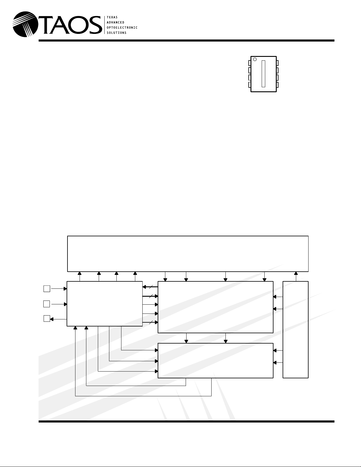
102 × 1 Sensor Element Organization
(TOP VIEW)
300 Dots-per-Inch Pixel Pitch
High Sensitivity
On-Chip 8-Bit Analog-to-Digital Conversion
Three-Zone Programmable Offset (Dark Level) and Gain
SCLK
VDD
SDIN
SDOUT
1
2
3
4
NC
8
GND
7
GND
6
NC
5
High Speed Serial Interface
1 MHz Pixel Rate
NC – No internal connection
Single 3-V to 5.5-V Supply
Description
The TSL3301 is a high-sensitivity 300-dpi, linear optical sensor array with integrated 8-bit analog-to-digital
converters. The array consists of 102 pixels, each measuring 85 µm (H) by 77 µm (W) and spaced on 85 µm
centers. Associated with each pixel is a charge integrator/amplifier and sample-hold circuit. All pixels have
concurrent integration periods and sampling times. The array is split into three 34-pixel zones, with each zone
having programmable gain and offset levels. Data communication is accomplished through a three-wire serial
interface.
Intended for use in high performance, cost-sensitive scanner applications, the TSL3301 is based on a linear
sensor array die that has expanded capability, including multi-die addressing and cascade options. Please
contact TAOS for additional information on die and multi-die package availability.
Functional Block Diagram
PIXCLK SI HOLD ZERO LEFT EVEN RIGHT ODD RIGHT EVEN IREF
SCLK
SDIN
SDOUT
DIGITAL I/O
AND
CONTROL
PIXEL ARRAY WITH INTEGRATORS AND S–H
(51-bit shift register)
8
DB<7:0>
5
ADDR<4:0>
READ
WRITE
3
SECTOR
RESET/SAMPLE
START
ADCLK
OUTPUT CHARGE-TO-
VOLTAGE CONVERTER
WITH PROGRAMMABLE
GAINS AND OFFSETS
DUAL 8–BIT
SA ADC
VREF
IREF
BIAS
BLOCK
VREF
IREF
www.taosinc.com
Texas Advanced Optoelectronic Solutions Inc.
800 Jupiter Road, Suite 205 Plano, TX 75074 (972) 673-0759
Copyright 2001, TAOS Inc.
1
TSL3301
102 × 1 LINEAR OPTICAL SENSOR ARRAY
WITH ANALOGTODIGITAL CONVERTER
TAOS026 – FEBRUARY 2001
Terminal Functions
TERMINAL
NAME NO.
GND 6, 7 Ground
SCLK 1 I System clock input for serial I/O and all internal logic.
SDIN 3 I Serial data input. Data is clocked in on the rising edge of SCLK.
SDOUT 4 O Serial data output. Data is clocked out on the falling edge of SCLK.
V
DD
I/O DESCRIPTION
2 Positive supply voltage.
Detailed Description
The TSL3301 is a 102 × 1 linear optical array with onboard A/D conversion. It communicates over a serial digital
interface and operates over a 3 V to 5.5 V range. The array is divided into three 34-pixel zones (left, center, and
right), with each zone having programmable gain and offset (dark signal) correction.
The sensor consists of 102 photodiodes, also called pixels, arranged in a linear array. Light energy impinging
on a pixel generates a photocurrent, which is then integrated by the active integration circuitry associated with
that pixel. During the integration period, a sampling capacitor connects to the output of the integrator through
an analog switch. The amount of charge accumulated at each pixel is directly proportional to the light intensity
(Ee) on that pixel and to the integration time (t
approximately 300 electrons.
Integration, sampling, output, and reset of the integrators are performed by the control logic in response to
commands input via the SDIN pin. Data is read out on the SDOUT pin. A normal sequence of operation consists
of a pixel reset (
(
SAMPLEInt
RESET
), start of integration (
), and pixel output (
READPixel
the integrators from the reset state and defines the beginning of the integration period. Sampling the integrators
ends the integration period and stores the charge accumulated in each pixel in a sample and hold circuit.
Reading the pixels causes the sampled value of each pixel to be converted to 8-bit digital format and output on
the SDOUT pin. All 102 pixels are output sequentially unless interrupted by an abort (
or reset by a
RESET
command.
). At maximum programmed gain, one LSB corresponds to
int
STARTInt
), integration period, sampling of integrators
). Reset sets all the integrators to zero. Start of integration releases
ABORTPixel
) command
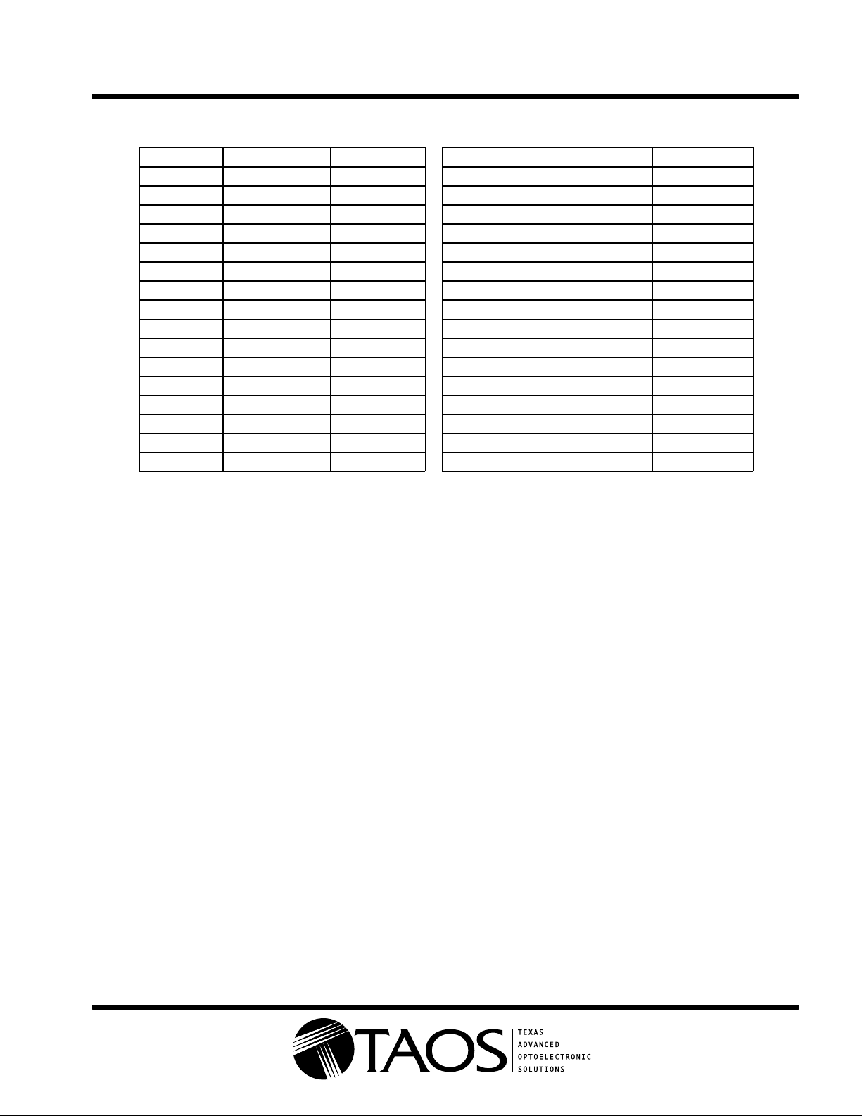
Gain adjustment is controlled by three 5-bit DACs, one for each of the the three zones. Table 1 lists the gain
settings and the corresponding pixel values. Offset is affected by the gain setting and may have to be adjusted
after gain changes are made.
Offset correction is controlled by three 8-bit sign-magnitude† DACs and is performed in the analog domain prior
to the digital conversion. There is a separate offset DAC for each of the three zones. Codes 0h – 7Fh correspond
to positive offset values and codes 80h – FFh correspond to negative offset values.
The offset correction is proportional to the gain setting. At minimal gain, one LSB of the offset DAC corresponds
to approximately 1/3 LSB of the device output, and at maximum gain, to about 1 LSB of the device output.
Note that the gain and offset registers are in indeterminate states after power up and must be set by the controller
as required.
†
Sign-magnitude is a binary representation in which the most significant bit (MSB) is used to represent the sign of the number, with the remaining
bits representing the magnitude. An MSB of 1 indicates a negative number.
Copyright 2001, TAOS Inc.
2
www.taosinc.com
102 × 1 LINEAR OPTICAL SENSOR ARRAY
WITH ANALOGTODIGITAL CONVERTER
TAOS026 – FEBRUARY 2001
Table 1. Gain Settings and Results
GAIN CODE RELATIVE GAIN % INCREASE GAIN CODE RELATIVE GAIN % INCREASE
0 1 16 1.52 3.23
1 1.02 2.17 17 1.57 3.33
2 1.05 2.22 18 1.62 3.45
3 1.07 2.27 19 1.68 3.57
4 1.09 2.33 20 1.74 3.70
5 1.12 2.38 21 1.81 3.85
6 1.15 2.44 22 1.88 4.00
7 1.18 2.50 23 1.96 4.17
8 1.21 2.56 24 2.05 4.35
9 1.24 2.63 25 2.14 4.55
10 1.27 2.70 26 2.24 4.76
11 1.31 2.78 27 2.35 5.00
12 1.34 2.86 28 2.48 5.26
13 1.38 2.94 29 2.61 5.56
14 1.43 3.03 30 2.77 5.88
15 1.47 3.13 31 2.94 6.25
TSL3301
Serial interface
The serial interface follows a USART format, with start bit, 8 data bits and one or more stop bits. Data is clocked
in synchronously on the rising edge of SCLK and clocked out on the falling edge of SCLK. Stop bits are not
required on the input. When clocking data out continuously (i.e., reading out pixels) there will be one stop bit
between data words.
The receive and transmit state machines are independent, which means commands can be issued while
reading data. This feature allows starting new integration cycles while reading data. Note that this allows
undefined conditions so care must be taken not to issue commands that will cause outputs (such as register
read) while reading out data. For instance, issuing a register read command while reading out image data will
result in garbage out. Likewise, it is possible to change offset and gain registers during a readout, which can
give unpredictable results.
It is not necessary to have a continuously active clock, but a minimum of 6 clocks is required after any command
has been issued to ensure that the corresponding internal logic actions have been completed. When reading
register contents, there will be a 4-clock delay from the completion of the
the register contents are output. When reading out pixel values, there will be a 44-clock delay from completion
of the
READPixel
to have 22 clocks to complete the pixel reset cycle (see
command until the first pixel data is output. When sampling pixel information it is necessary
Imaging
below).
REGRead
command before
www.taosinc.com
Copyright 2001, TAOS Inc.
3
TSL3301
102 × 1 LINEAR OPTICAL SENSOR ARRAY
WITH ANALOGTODIGITAL CONVERTER
TAOS026 – FEBRUARY 2001
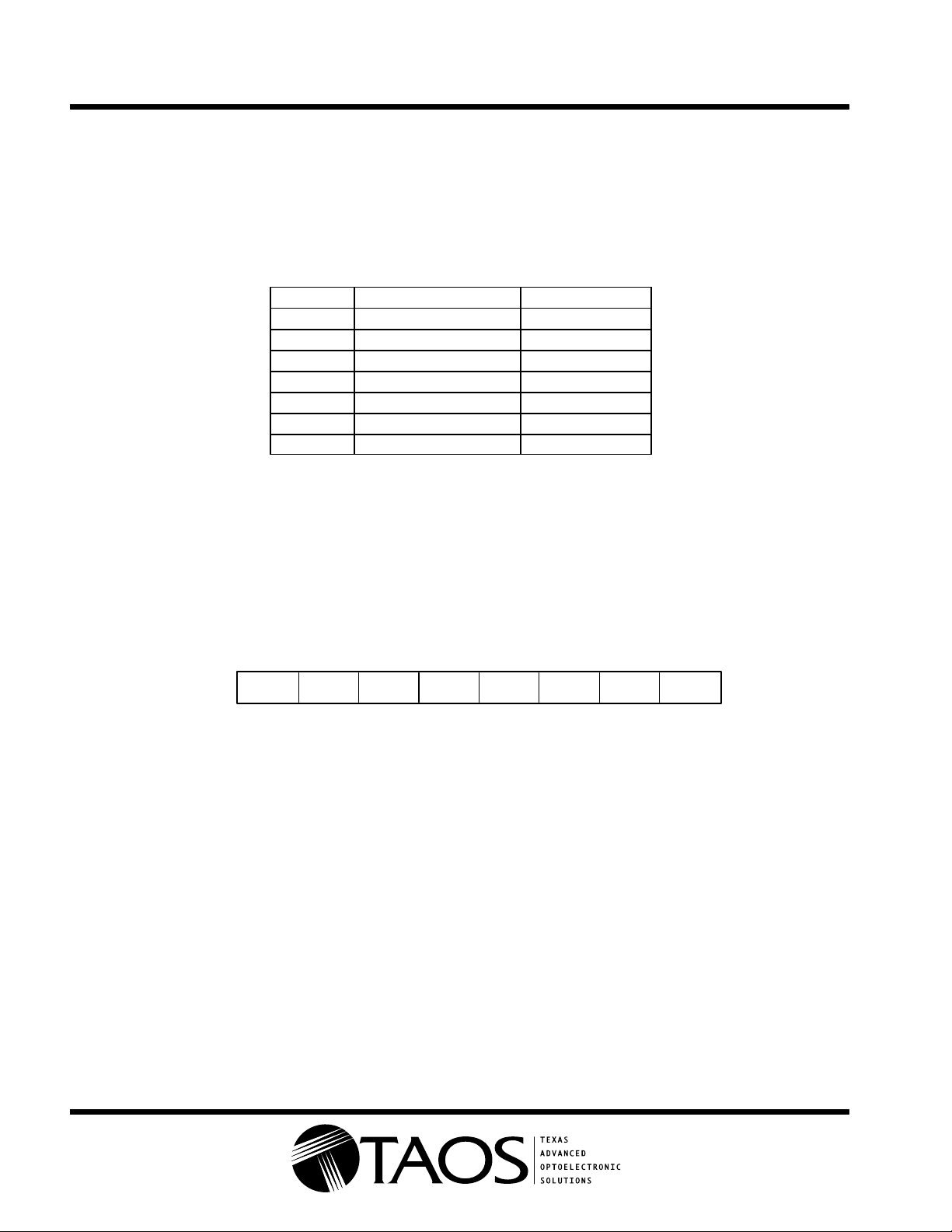
Register address map
The TSL3301 contains seven registers as defined in Table 2. Data in these registers may be written to or read
from using the
converters (ADC). Three other registers allow the offset of the system to be adjusted. Together the gain and
offset registers are used to maximize the achievable dynamic range.
REGWrite
and
REGRead
commands. Three registers control the gain of the analog-to-digital
Table 2. Register Address Map
ADDRESS REGISTER DESCRIPTION REGISTER WIDTH
0x00 Left (pixels 0–33) offset 8
0x01 Left (pixels 0–33) gain 5
0x02 Center (pixels 34–67) offset 8
0x03 Center (pixels 34–67) gain 5
0x04 Right (pixels 68–101) offset 8
0x05 Right (pixels 68–101) gain 5
0x1F Mode 8
The offset registers are 8-bit sign-magnitude values and the gain registers are 5-bit values. The programmed
offset correction is applied to the sampled energy, and then the gain is applied. (i.e., the gain will affect the offset
correction.) These registers allow the user to maximize the dynamic range achievable in the given system.
The last register is the mode register. Bits in this register select the sleep mode as well as options for multichip
arrays and production testing. Note that test and multichip options do not apply to the 8-pin packaged device.
Users should always write zeros into the production test and multichip control bits.
654321
0x1F
SLP = Sleep Mode:
1
places device into sleep mode
0
places device in normal operating mode
P2 MODE0 0 SLP P1 P0 C1 C0
C1, C0 selects multichip options (should be written
P2 to P0 are factory test bits (should be written
07
0
)
0
)
Figure 1. Mode Register Bit Assignments
Copyright 2001, TAOS Inc.
4
www.taosinc.com
Command description
TSL3301
102 × 1 LINEAR OPTICAL SENSOR ARRAY
WITH ANALOGTODIGITAL CONVERTER
TAOS026 – FEBRUARY 2001
The TSL3301 is a
slave
device that reacts strictly to commands received from the digital controller. These
commands cause the device to perform functions such as reset, integrate, sample, etc. Table 3 summarizes
the command types and formats and Table 4 lists the command set for the TSL3301. Each command is
described in more detail below.
Table 3. Command Type and Format Summary
COMMAND TYPE FORMAT
Action command < Command byte >
Register write < Command byte > < Data byte >
Table 4. TSL3301 Command Set
COMMAND DESCRIPTION
IRESET Interface Reset
RESET Reset Integration and read blocks
DETReset Reset determine unique address block
STARTInt Start pixel integration
SAMPLEInt Stop light integration and sample results
READPixel Dump serial the contents of each sampled integrator
ABORTPixel Abort any READPixel operation in progress
READHold Combination of SAMPLEInt and READPixel commands
READHoldNStart Combination of SAMPLEInt, READPixel and STARTInt commands
REGWrite Write a gain, offset, or mode register
REGRead Read a gain, offset, or mode register
www.taosinc.com
Copyright 2001, TAOS Inc.
5
 Loading...