


TAOS TSL230RP, TSL230BRP, TSL230ARP Datasheet

TSL230R, TSL230AR, TSL230BR
PROGRAMMABLE LIGHTTOFREQUENCY CONVERTERS
TAOS048 – OCTOBER 2002
8-LEAD PDIP
S0
S1
OE
GND
PACKAGE P
(TOP VIEW)
8
2
7
3
6
4
5
S3
S2
OUT
V
DD
High-Resolution Conversion of Light
Intensity to Frequency With No External
Components
Programmable Sensitivity and Full-Scale
Output Frequency
Communicates Directly With a Microcontroller
Single-Supply Operation Down to 2.7 V,
With Power-Down Feature
Absolute Output Frequency Tolerance of
±5% (TSL230BR)
Nonlinearity Error Typically 0.2% at 100 kHz
Stable 150 ppm/°C Temperature Coefficient
Replacements for TSL230, TSL230A, and
TSL230B
Description
The TSL230R, TSL230AR, and TSL230BR programmable light-to-frequency converters combine a
configurable silicon photodiode and a current-to-frequency converter on single monolithic CMOS integrated
circuits. The output can be either a pulse train or a square wave (50% duty cycle) with frequency directly
proportional to light intensity. Device sensitivity is selectable in three ranges, providing two decades of
adjustment. The full-scale output frequency can be scaled by one of four preset values. All inputs and the output
are TTL compatible, allowing direct two-way communication with a microcontroller for programming and output
interface. An output enable (OE) is provided that places the output in the high-impedance state for multiple-unit
sharing of a microcontroller input line.
The devices are available with absolute-output-frequency tolerances of ±5% (TSL230BR), ±10% (TSL230AR),
or ±20% (TSL230R). They have been temperature compensated for the ultraviolet-to-visible light range of
320 nm to 700 nm and respond over the light range of 320 nm to 1050 nm. The devices are characterized over
the temperature range of –25°C to 70°C.
Functional Block Diagram
Light
The
LUMENOLOGY
Company
Texas Advanced Optoelectronic Solutions Inc.
800 Jupiter Road, Suite 205 Plano, TX 75074 (972) 673-0759
Photodiode Array
S0 S1 S2 S3
www.taosinc.com
Current-to-Frequency
Output
Converter
OE
Copyright 2002, TAOS Inc.
1
TSL230R, TSL230AR, TSL230BR
PROGRAMMABLE LIGHTTOFREQUENCY CONVERTERS
TAOS048 – OCTOBER 2002
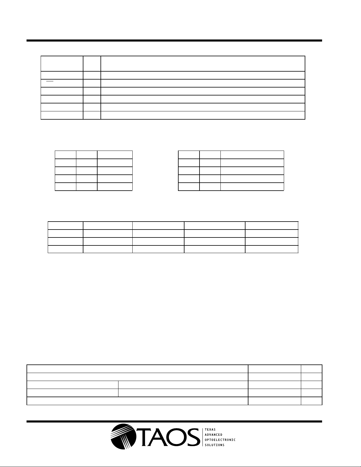
Terminal Functions
TERMINAL
NAME NO.
GND 4 Ground
OE 3 I Enable for fO (active low)
OUT 6 O Scaled-frequency (fO) output
S0, S1 1, 2 I Sensitivity-select inputs
S2, S3 7, 8 I fO scaling-select inputs
V
DD
5 Supply voltage
Selectable Options
S1 S0 SENSITIVITY S3 S2 fO SCALING (divide-by)
L L Power down
L H 1× L H 2
H L 10× H L 10
H H 100× H H 100
Available Options
DEVICE T
TSL230R –25°C to 85° PDIP–8 P TSL230RP
TSL230AR –25°C to 85° PDIP–8 P TSL230ARP
TSL230BR –25°C to 85° PDIP–8 P TSL230BRP
TYPE DESCRIPTION
L L 1
A
PACKAGE – LEADS PACKAGE DESIGNATOR ORDERING NUMBER
Absolute Maximum Ratings over operating free-air temperature range (unless otherwise noted)
Supply voltage, VDD (see Note 1) 6 V. . . . . . . . . . . . . . . . . . . . . . . . . . . . . . . . . . . . . . . . . . . . . . . . . . . . . . . . . . . . .
Input voltage range, all inputs, VI –0.3 V to VDD + 0.3 V. . . . . . . . . . . . . . . . . . . . . . . . . . . . . . . . . . . . . . . . . . . . .
Operating free-air temperature range, TA –25°C to 70°C. . . . . . . . . . . . . . . . . . . . . . . . . . . . . . . . . . . . . . . . . . . .
Storage temperature range –25°C to 85°C. . . . . . . . . . . . . . . . . . . . . . . . . . . . . . . . . . . . . . . . . . . . . . . . . . . . . . . .
Lead temperature 1,6 mm (1/16 inch) from case for 10 seconds 260°C. . . . . . . . . . . . . . . . . . . . . . . . . . . . . . .
†
Stresses beyond those listed under “absolute maximum ratings” may cause permanent damage to the device. These are stress ratings only, and
functional operation of the device at these or any other conditions beyond those indicated under “recommended operating conditions” is not
implied. Exposure to absolute-maximum-rated conditions for extended periods may affect device reliability.
NOTE 1: All voltage values are with respect to GND.
Recommended Operating Conditions
MIN NOM MAX UNIT
Supply voltage, V
High-level input voltage, V
Low-level input voltage, V
Operating free-air temperature range, T
Copyright 2002, TAOS Inc.
DD
IH
IL
VDD = 4.5 V to 5.5 V 2 V
VDD = 4.5 V to 5.5 V 0 0.8 V
A
2.7 5 5.5 V
DD
–25 70 °C
The
LUMENOLOGY
Company
V
†
2
www.taosinc.com
TSL230R, TSL230AR, TSL230BR
Out ut ulse
Nonlinearity
PROGRAMMABLE LIGHTTOFREQUENCY CONVERTERS
TAOS048 – OCTOBER 2002
Electrical Characteristics at TA = 25°C, VDD = 5 V (unless otherwise noted)
PARAMETER TEST CONDITIONS MIN TYP MAX UNIT
V
OH
V
OL
I
IH
I
IL
I
DD
F.S. Full-scale frequency
k
SVS
†
Full-scale frequency is the maximum operating frequency of the device without saturation.
Operating Characteristics at VDD = 5 V , TA = 25°C, Ee = 130 µW/cm2, λp = 640 nm (unless otherwise
noted)
fOOutput frequency S0 = S1 = S2 = H,
ReResponsivity
t
w
‡
Nonlinearity is defined as the deviation of fO from a straight line between zero and full scale, expressed as a percent of full scale.
#
Nonlinearity test condition: S0 = S1 = H, S2 = S3 = L.
§
Principal frequency is the internal oscillator frequency, equivalent to divide-by-1 output selection.
High-level output voltage IOH = –4 mA 4 4.5 V
Low-level output voltage IOL = 4 mA 0.25 0.4 V
High-level input current 5 µA
Low-level input current 5 µA
Supply current
†
Power-on mode 2 3 mA
Power-down mode 5 12 µA
1.1 MHz
Temperature coefficient of output frequency λ ≤ 700 nm ±150 ppm/°C
Supply voltage sensitivity VDD = 5 V ±10% ±0.5 %/V
PARAMETER TEST CONDITIONS
S0 = S1 = H,
S2 = S3 = L
S1 = H,
S0 = S2 = S3 = L
S0 = H,
S1 = S2 = S3 = L
S3 = L
S0 = S1 = S3 = H,
S2 = L
TSL230R TSL230AR TSL230BR
MIN TYP MAX MIN TYP MAX MIN TYP MAX
80 100 120 90 100 110 95 100 105 kHz
8 10 12 9 10 11 9.5 10 10.5 kHz
0.8 1 1.2 0.9 1 1.1 0.95 1 1.05 kHz
40 50 60 45 50 55 47.5 50 52.5 kHz
8 10 12 9 10 11 9.5 10 10.5 kHz
S0 = S1 = S2 = S3 = H 0.8 1 1.2 0.9 1 1.1 0.95 1 1.05 kHz
Output pulse
duration
Nonlinearity
‡#
Recovery from
power down
Step response to
full-scale step input
Response time to
programming
Ee = 0, S0 = S1 = H,
S2 = S3 = L
S0 = S1 = H,
S2 = S3 = L
S2 = S3 = L 125 600 125 600 125 600 ns
S2 or S3 = H 1/2f
f
= 0 MHz to 10 kHz ±0.1% ±0.1% ±0.1% %F.S.
O
f
= 0 MHz to 100 kHz ±0.2% ±0.2% ±0.2% %F.S.
O
f
= 0 MHz to 1 MHz ±0.5% ±0.5% ±0.5% %F.S.
O
0.4 10 0.4 10 0.4 10 Hz
0.77 0.77 0.77
O
1/2f
O
1/2f
O
100 100 100 µs
1 pulse of new frequency plus 1 µs
2 periods of new principal frequency plus 1 µs
§
change
Response time to
output enable (OE)
50 150 50 150 50 150 ns
UNIT
kHz/
(µJ/
cm2)
s
The
LUMENOLOGY
Company
www.taosinc.com
Copyright 2002, TAOS Inc.
3