

TAOS TSL2014 Datasheet
TSL2014
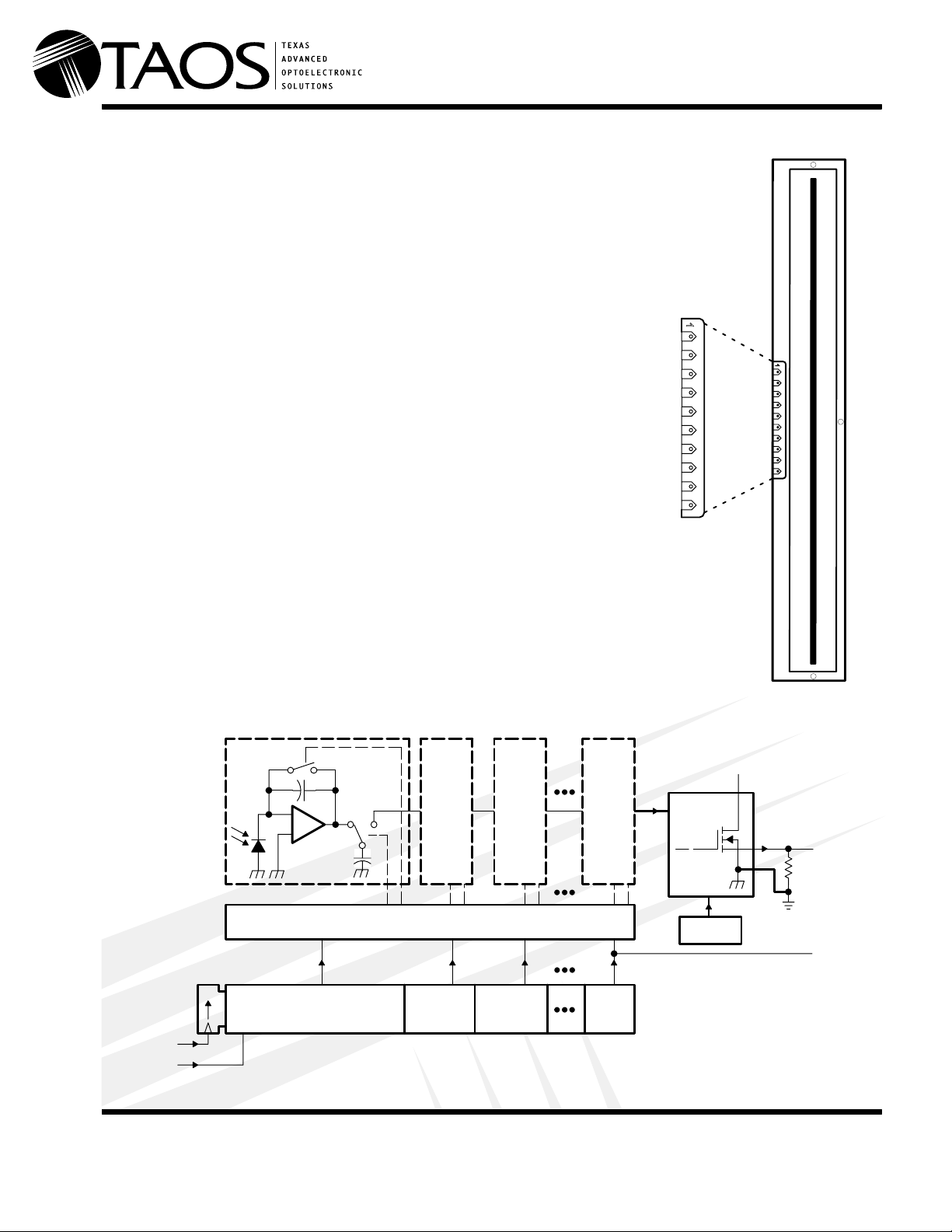
896 1 LINEAR SENSOR ARRAY
TAOS040 – AUGUST 2002
896 × 1 Sensor-Element Organization
200 Dots-Per-Inch (DPI) Sensor Pitch
High Linearity and Uniformity
Wide Dynamic Range...2000:1 (66 dB)
Output Referenced to Ground
Low Image Lag . . . 0.5% Typ
Operation to 5 MHz
Single 5-V Supply
112 mm Active Length
Description
The TSL2014 linear sensor array consists of two
sections of 448 photodiodes and associated charge
amplifier circuitry that can be connected to form a
contiguous 896 × 1 array. The pixels measure 120 µm
(H) by 70 µm (W) with 125-µm center-to-center spacing
and 55-µm spacing between pixels. Operation is
simplified by internal control logic that requires only a
serial-input (SI) signal and a clock.
The TSL2014 is intended for use in a wide variety of
applications including mark detection and code
reading, optical character recognition (OCR) and
contact imaging, edge detection and positioning as well
as optical linear and rotary encoding.
V
DD
SI1 2
AO1 3
SO1 4
SI2 5
CLK 6
GND 7
AO2 8
SO2 9
V
10
DD
PACKAGE
(TOP VIEW)
1
Functional Block Diagram (each section)
Pixel 1 (449)
Integrator
Reset
_
+
Sample/
Output
Switch Control Logic
CLK 448-Bit Shift Register
SI1 (SI2)
The
LUMENOLOGY
Company
Texas Advanced Optoelectronic Solutions Inc.
800 Jupiter Road, Suite 205 Plano, TX 75074 (972) 673-0759
Pixel
2
(450)
www.taosinc.com
Pixel
(451)
3
Q3Q2Q1
Pixel
448
(896)
Analog
Bus
Q448 (896)
Output
Amplifier
Gain Trim
V
DD
AO1
(AO2)
R
L
External
Load
SO1
(SO2)
Copyright 2002, TAOS Inc.
1
TSL2014
896 1 LINEAR SENSOR ARRAY
TAOS040 – AUGUST 2002
Terminal Functions
TERMINAL
NAME NO.
AO1 3 O Analog output of section 1.
AO2 8 O Analog output of section 2.
CLK 6 I Clock. The clock controls the charge transfer, pixel output and reset.
GND 7 Ground (substrate). All voltages are referenced to GND.
SI1 2 I Serial input (section 1). SI1 defines the start of the data-out sequence.
SI2 5 I Serial input (section 2). SI2 defines the start of the data-out sequence.
SO1 4 O
SO2 9 O
VDD 1, 10 Supply voltage. Supply voltage for both analog and digital circuits.
I/O DESCRIPTION
Serial output (section 1). SO1 signals the end of the data out sequence and provides a signal to drive the input
of section 2 (SI2) in serial mode.
Serial output (section 2). SO2 signals the end of the data out sequence and provides a signal to drive the input
of another device for cascading.
Detailed Description
The sensor consists of 896 photodiodes arranged in a linear array. Light energy impinging on a photodiode
generates photocurrent, which is integrated by the active integration circuitry associated with that pixel. During
the integration period, a sampling capacitor connects to the output of the integrator through an analog switch.
The amount of charge accumulated at each pixel is directly proportional to the light intensity and the integration
time. The integration time is the interval between two consecutive output periods.
The output and reset of the integrators is controlled by two 448-bit shift registers and reset logic. A 448-pixel
output cycle is initiated by clocking in a logic 1 into the SI input of a section for one positive going clock edge
(see Figures1 and 2)†. The two 448-pixel sections may be operated independently using a single clock input
or connected in series to form a 896-pixel array. Each section has an independent output (AO), which may be
connected together for the 896-pixel function.
When operating in the 896-pixel mode, as the SI pulse is clocked through the 896-bit shift register, the charge
on the sampling capacitor of each pixel is sequentially connected to a charge-coupled output amplifier that
generates a voltage output, AO. When the bit position goes low, the pixel integrator is reset. On the 897th clock
rising edge, the SI pulse is clocked out of the shift register (S2) and the output assumes a high-impedance state.
Note that this 897th clock pulse is required to terminate the output of the 896th pixel and return the internal logic
to a known state. A subsequent SI pulse can be presented as early as the 898th clock pulse, thereby initiating
another pixel output cycle.
The voltage developed at analog output (AO) is given by:
V
= V
out
+ (Re) (Ee) (t
drk
)
int
where:
V
out
V
drk
R
E
e
t
int
is the analog output voltage for white condition
is the analog output voltage for dark condition
is the device responsivity for a given wavelength of light given in V/(µJ/cm2)
e
is the incident irradiance in µW/cm
2
is integration time in seconds
AO is driven by a source follower that requires an external pulldown resistor (330-Ω typical). The output is
nominally 0 V for no light input, 2 V for normal white-level, and 3.4 V for saturation light level. When the device
is not in the output phase, AO is in a high impedance state.
A 0.1 µF bypass capacitor should be connected between VDD and ground as close as possible to the device.
†
For proper operation, after meeting the minimum hold time condition, SI must go low before the next rising edge of the clock.
Copyright 2002, TAOS Inc.
The
LUMENOLOGY
Company
2
www.taosinc.com
TSL2014
896 1 LINEAR SENSOR ARRAY
TAOS040 – AUGUST 2002
Absolute Maximum Ratings
†
Supply voltage range, VDD –0.3 V to 6 V. . . . . . . . . . . . . . . . . . . . . . . . . . . . . . . . . . . . . . . . . . . . . . . . . . . . . . . . . . .
Input voltage range, VI –0.3 V to VDD + 0.3V. . . . . . . . . . . . . . . . . . . . . . . . . . . . . . . . . . . . . . . . . . . . . . . . . . . . . .
Input clamp current, IIK (VI < 0 or VI > VDD) –20 mA to 20 mA. . . . . . . . . . . . . . . . . . . . . . . . . . . . . . . . . . . . . . . .
Output clamp current, IOK (VO < 0 or VO > VDD) –25 mA to 25 mA. . . . . . . . . . . . . . . . . . . . . . . . . . . . . . . . . . . .
Voltage range applied to any output in the high impedance or
power-off state, VO –0.3 V to VDD + 0.3V. . . . . . . . . . . . . . . . . . . . . . . . . . . . . . . . . . . . . . . . . . . . . . . . . . .
Continuous output current, I
(V
= 0 to VDD) –25 mA to 25 mA. . . . . . . . . . . . . . . . . . . . . . . . . . . . . . . . . . . . . .
O
O
Continuous current through VDD or GND –150 mA to 150 mA. . . . . . . . . . . . . . . . . . . . . . . . . . . . . . . . . . . . . . .
Analog output current range, IO –25 mA to 25 mA. . . . . . . . . . . . . . . . . . . . . . . . . . . . . . . . . . . . . . . . . . . . . . . . . .
Operating free-air temperature range, TA –25°C to 85°C. . . . . . . . . . . . . . . . . . . . . . . . . . . . . . . . . . . . . . . . . . . .
Storage temperature range, T
–25°C to 85°C. . . . . . . . . . . . . . . . . . . . . . . . . . . . . . . . . . . . . . . . . . . . . . . . . . . .
stg
Lead temperature on solder pads for 10 seconds 260°C. . . . . . . . . . . . . . . . . . . . . . . . . . . . . . . . . . . . . . . . . . . .
ESD tolerance, human body model 2000 V. . . . . . . . . . . . . . . . . . . . . . . . . . . . . . . . . . . . . . . . . . . . . . . . . . . . . . . .
†
Stresses beyond those listed under “Absolute Maximum Ratings” may cause permanent damage to the device. These are stress ratings only, and
functional operation of the device at these or any other conditions beyond those indicated under “Recommended Operating Conditions” is not
implied. Exposure to absolute-maximum-rated conditions for extended periods may affect device reliability.
Recommended Operating Conditions (see Figure 1 and Figure 2)
MIN NOM MAX UNIT
Supply voltage, V
Input voltage, V
High-level input voltage, V
Low-level input voltage, V
Wavelength of light source, λ 400 1000 nm
Clock frequency, f
Sensor integration time, serial t
Sensor integration time, parallel t
Operating free-air temperature, T
Load resistance, R
Load capacitance, C
DD
I
IH
IL
clock
int
int
A
L
L
4.5 5 5.5 V
0 V
2 V
0 0.8 V
5 5000 kHz
0.1792 100 ms
0.090 100 ms
0 70 °C
300 4700 Ω
DD
DD
330 pF
V
V
The
LUMENOLOGY
Company
www.taosinc.com
Copyright 2002, TAOS Inc.
3
 Loading...