

Tandy 102, 26-3803 Service Manual
TANDY®
of
0
0
•
CUSTOM MANUFACTURED FOR RADIO SHACK, A DIVISION OF TANDY CORPORATION

á

CONTENTS
PART I. INTRODUCTION ........................................................................................ 1-1
System Overview ............................................................................................. 1-2
External View .................................................................................................... 1-2
Internal View ..................................................................................................... 1-5
Specifications ................................................................................................... 1-7
PART 11. DISASSEMBLY INSTRUCTIONS ............................................................. 2-1
Cases ................................................................................................................. 2-1
Keyboard and LCD PCBs ................................................................................. 2-1
Main PCB ........................................................................................................... 2-2
PART III. MAINTENANCE ....................................................................................... 3-1
To clean the body and LCD display ................................................................ 3-1
PART IV. THEORY OF OPERATION ....................................................................... 4-1
General .............................................................................................................. 4-1
Block Diagram .................................................................................................. 4-2
CPU .................................................................................................................... 4-3
Memory ............................................................................................................. 4-3
I/O Map ............................................................................................................. 4-5
Keyboard .......................................................................................................... 4-6
Cassette Interface Circuit ............................................................................... 4-7
Printer Interface Circuit ................................................................................... 4-8
Bar Code Reader Interface Circuit ................................................................. 4-9
Buzzer Control Circuit ...................................................................................... 4-10
System Bus ....................................................................................................... 4-11
Clock Control Circuit ....................................................................................... 4-12
Serial Interface Circuit ..................................................................................... 4-14
LCD .................................................................................................................... 4-21
Power Supply Circuit ....................................................................................... 4-24
PART V. TROUBLESHOOTING .............................................................................. 5-1
General Guidance ............................................................................................ 5-1
Troubleshooting Guide .................................................................................... 5-1
Check List ......................................................................................................... 5-11
PART VI. EXPLODED VIEW/PARTS LIST ............................................................. 6-1
Electrical Parts List .......................................................................................... 6-2
Mechanical and Assembly Parts List ............................................................. 6-11
PART VII. SCHEMATIC DIAGRAMS/ PCB VIEWS ................................................ 7-1
Schematic Diagrams ........................................................................................ 7-1
PCB Views ......................................................................................................... 7-3
APPENDIX A/ INSTALLATION ............................................................................ A-1
Installation of Optional RAM and ROM .......................................................... A-1
APPENDIX B/ KEYBOARD LAYOUT, CONNECTOR PIN
ASSIGNMENTS AND CHARACTER CODE TABLE ....................... B-1
B-1. Keyboard Layout ..................................................................................... B-1
B-2. Connector Pin Assignments ................................................................... B-2
B-3. Character Code Table ............................................................................. B-7
APPENDIX C/ TECHNICAL INFORMATION .......................................................... C-1
C-1. 80C85A .................................................................................................... C-1
C-2. 81 C55 ....................................................................................................... C-7
C-3. 6402 ......................................................................................................... C-13
C-4. Basic Construction of LCD ..................................................................... C-19
io
List of Illustrations
FIGURE
DESCRIPTION
PAGE
NUMBER NUMBER
1-1
Front View ................................................................................................................................
1-2
1-2
Rear View ................................................................................................................................
1-3
1-3
Bottom View ............................................................................................................................
1-4
1-4
Main PCB (Bottom View) .......................................................................................................
1-5
1-5
LCD PCB .................................................................................................................................
1-6
2-1
Top Case Removal .................................................................................................................
2-1
2-2 Keyboard and LCP PCBs Removal .......................................................................................
2-1
2-3 Main PCB Removal .................................................................................................................
2-4
4-1
Organization of Section IV .....................................................................................................
4-1
4-2
System Block Diagram ...........................................................................................................
4-2
4-3 Functional Block Diagram of Bus Separation Circuit ...........................................................
4-3
4-4 Memory Map ...........................................................................................................................
4-3
4-5
Address Decoding and Bank Selection Circuit ....................................................................
4-4
4-6 I/O Address Decoding Circuit ................................................................................................
4-5
4-7
Condition of Pressing
"T"
Key ...............................................................................................
4-6
4-8
Cassette Interface Circuit .......................................................................................................
4-7
4-9 Printer Interface Circuit ..........................................................................................................
4-8
4-10 Bar Code Reader Interface Circuit ........................................................................................
4-9
4-11 Buzzer Control Circuit ............................................................................................................
4-10
4-12
Time Set Sequence ofuPD1990AC .......................................................................................
4-12
4-13
Time Read Sequence ofuPD1990AC ...................................................................................
4-13
4-14
Functional Block Diagram of the Serial Interface .................................................................
4-14
4-15
RS-232C/MODEM Selection Circuit ......................................................................................
4-15
4-16
RS-232C Interface Circuit ......................................................................................................
4-16
4-17 MODEM IC and Peripheral Circuit .........................................................................................
4-17
4-18 Transmission Filter Circuit .....................................................................................................
4-17
4-19
Reception Filter Circuit ...........................................................................................................
4-18
4-20 MODEM Adjustment ...............................................................................................................
4-19
4-21 MODEM Connector Interface Circuit ....................................................................................
4-20
4-22
HD44103 Internal Logic Diagram ..........................................................................................
4-21
4-23
HD44102 Internal Logic Diagram ..........................................................................................
4-22
4-24 LCD Waveform ........................................................................................................................
4-23
4-25 Power Supply and Reset Circuit ............................................................................................
4-25
6-1
Exploded View ........................................................................................................................
6-1
7-1
Main PCB - Schematic Diagram ............................................................................................
7-1
7-2
LCD PCB - Schematic Diagram ............................................................................................
7-2
7-3
Main PCB - Top View .............................................................................................................
7-3
7-4
Main PCB - Bottom View ........................................................................................................
7-4
7-5 LCD PCB - Top View ..............................................................................................................
7-5
A-1 Installation of RAM and ROM ................................................................................................. A-1
B-1 Keyboard Layout .................................................................................................................... B-1
B-2 System Bus Connector ........................................................................................................... B-2
B-3 RS-232C Connector ............................................................................................................... B-3
B-4 Printer Connector ................................................................................................................... B-4
B-5 Cassette Connector ................................................................................................................ B-5
B-6 MODEM Connector ................................................................................................................ B-5
B-7 Bar Code Reader Connector ................................................................................................. B-6
C-1 Functional Block Diagram ...................................................................................................... C-1
C-2 Pin Configuration of 80C85A ................................................................................................. C-1
C-3 Trap and RESET IN ................................................................................................................. C-5
C-4 80C85A Basic System Timing ............................................................................................... C-7
C-5 Functional Block Diagram ..................................................................................................... C-7
iii
FIGURE
DESCRIPTION
NUMBER NUMPAGEBER
..................................
C-6 Pin Configuration of 81 C55 .................................................................. C-7
C-7 Internal Register of 81 C55 ..................................................................................................... C-9
C-8 Programming the Command/Status Register ...................................................................... C-10
C-9 Reading the C/S Register ....................................................................................................... C-11
C-10 Bit Assignments to the Timer Counter .................................................................................. C-11
C-11 Functional Block Diagram ...................................................................................................... C-13
C-12 Pin Configuration of 6402 ....................................................................................................... C-13
C-,13 Receiver Timing ..................................................................................................................... C-16
C-14 Transmitter Operation ............................................................................................................ C-17
C-15 Start Bit Detection Timing ...................................................................................................... C-18
C-16 Construction of LCD Panel .................................................................................................... C-19
C-17 Operation Theory of LCD Panel ............................................................................................. C-20
List of Tables
TABLE
NUMBER
DESCRIPTION
NUMPAGEBER
4-1 I/O MAP ................................................................................................................................... 4-5
4-2 Port Address of PIO ................................................................................................................ 4-5
4-3 System Bus Pin Assignments ................................................................................................ 4-11
B-1 System Bus Connector Pin Assignments ............................................................................. B-2
B-2 RS-233C Connector Pin Assignments .................................................................................. B-3
B-3 Printer Connector Pin Assignments ...................................................................................... B-4
C-1 Interrupt Priority, Restart Address and Sensitivity ............................................................... C-4
C-2 80C85A Machine Cycle Chart ............................................................................................... C-6
C-3 80C85A Machine State Chart ................................................................................................ C-6
C-4 I/O Address of 81 C55 ............................................................................................................. C-9
C-5 Port Control Assignment ........................................................................................................ C-10
C-6 Control Word Format .............................................................................................................. C-15
iv
I. INTRODUCTION
This manual is prepared for the Tandy 102 technicians working in field or in repair centers. Users of
this manual should be acquainted with the 80C85A microprocessor, the 81 C55 PIO and the 6402
UART. If you need more detailed information, refer to Appendix C in this manual.
This manual consists of seven sections and three appendices:
Section I
This section provides general information on the Tandy 102 such as specifications, external
views and internal views.
Section II
This section describes the disassembly procedures.
Section III
This section describes the maintenance of the Tandy 102.
Section IV
This section describes the general theory of operation for the Tandy 102.
Section V
This section describes how to troubleshoot the Tandy 102.
Section VI
This section provides an exploded view and parts list of the Tandy 102.
Section VII
This section provides the schematics, PCB diagrams, and silkscreen views of the PCBs of the
Tandy 102.
Appendix A
This appendix provides instructions for installing the optional ROM and additional RAMs.
Appendix B
This appendix provides the character code table, keyboard layouts and connector pin
assignments.
Appendix C
This appendix provides the technical information of the 80C85A, 81 C55, 6402 and LCD.
System Overview
Tandy 102 portable computer is a low cost version of the Radio Shack TRS-80 Model 100 Portable
Computer. The Tandy 102 is fully compatible with the Model 100 in its software so that both system
users can take advantage of the large number of programs available.
The Tandy 102 has the following applications programs in the standard ROM: BASIC, TEXT,
TELCOM, ADDRSS, SCHEDL and TELCOM.
External View
1 Keyboard: Can be used like the standard typewriter. However, the Tandy 102 does have a few
speciatkeys. (See Appendix B of this manual for more details.)
2 LCD Screen: The Tandy 102 display has eight lines that allow 40 characters on each line.
3 Power Switch: Move this switch towards the front to turn the power on. To conserve the
batteries, the Tandy 102 automatically turns the power off if you do not use it for 10 minutes in
default setting.
4 Low Battery Indicator: Before the Tandy 102 is operational batteries become exhausted, this
indicator will illuminate.
5 Display Adjustment Dial: This control adjusts the contrast of the LCD display relative to the
viewing angle.
6 External Power Adapter Connector: Connect the appropriate and of Radio Shack's AC Power
Supply (Catalog Number 26-3804, optional/extra) to this connector. Connect the other end of
the power supply to a standard AC wall-outlet or approved power strip.
1 Keyboard 2 LCD Screen 4 Low Battery
Indicator
11-1 11-1
1-1
N,
11-1
ZZ
6 External Power Adapter
Connector
5 Display Adjustment
Dial
3 Power Switch
Figure 1-1. Front View
1-2
1 RESET Switch: If the Tandy 102 "locks up" (i.e., the display "freezes" and all keys seem to be
inoperative), press this button to return to the Main Menu (start-up). It is not likely that the
Tandy 102 will lock-up when you are using the built-in applications programs, however, it may
occur with customized programs.
2 RS-232C Connector: Attach a DB-25 cable (such as Radio Shack Catalog Number 26-1408) to
this connector when you need to receive or transmit serial information. When you
communicating directly with another TRS-80 computer, a Null MODEM Adapter (26-1496) is
required. An 8" Cable Extender (26-1497) may also be required.
3 SYSTEM BUS Connector: Connect this connector to the TRS-80 Disk/Video interface
(26-3806), using the system bus cable.
4 PRINTER Connctor: For hard-copy printouts of information, attach any Radio Shack parallel
printer to this connector, using an optional/extra printer cable.
5 Direct-Connect MODEM (PHONE) Connector: When communicating with another computer via
the Tandy 102's built-in MODEM, connect the round end of the optional/extra MODEM cable
to this connector.
6 CASSETTE Recorder Connector: To save or load information, on a cassette tape, connect the
cassette recorder here. An optional/extra cassette recorder (and cable) is required.
7 Bar Code Wand Connector: Attach the optional/extra bar code wand to this connector. Note
that special bar code reader software is required.
8 DIR/ACP Selector: This selector allows you to select either a direct or acoustic coupler
connection. If you are communicating with another computer over the phone lines via the
built-in, direct-connect MODEM, set this switch to the DIR position. If you are using the
optional/extra Model 100 Acoustic Coupler (26-3805), set this connector to the ACP position.
9 ANS/ ORIG Selector: If you are "originating" a phone call to another computer, set this switch
to ORIG. If another computer is calling your Tandy 102, set to ANS.
5 Direct-Connect
MODEM (PHONE) Connector
6 CASSETTE Recorder
Connector
4 PRINTER Connector
3 SYSTEM BUS Connector
1 RESET Switch
2 RS-232C Connector
Figure 1-2. Rear View
9 ANS/ORIG Selector
8 DIR/ACP Selector
7 Bar Code Wand
Connector
1-3
1 MEMORY POWER Switch: This switch is used to prevent discharge of the internal
Nickel-Cadmium battery, which is used for RAM back-up. The Tandy 102 will operate only
when the power switch is set to ON. Set this switch to the OFF position when the Tandy 102 will
not be used for a long period of time. Note that the RAM will not be backed up when this switch
is set to the OFF position.
2 Optional ROM and RAM Compartment: An optional/extra ROM and RAM can be inserted into
this compartment to enhance the Tandy 102 capabilities.
3 Battery Compartment : When not connected to an AC power source, the Tandy 102 gets its
power from four AA size batteries that must be installed in this compartment.
3 BATTERY Compartment
1 MEMORY POWER 2 OPTIONAL ROM and RAM
Switch Compartment
X
X
11
O
O®
Figure 1-3. Bottom View
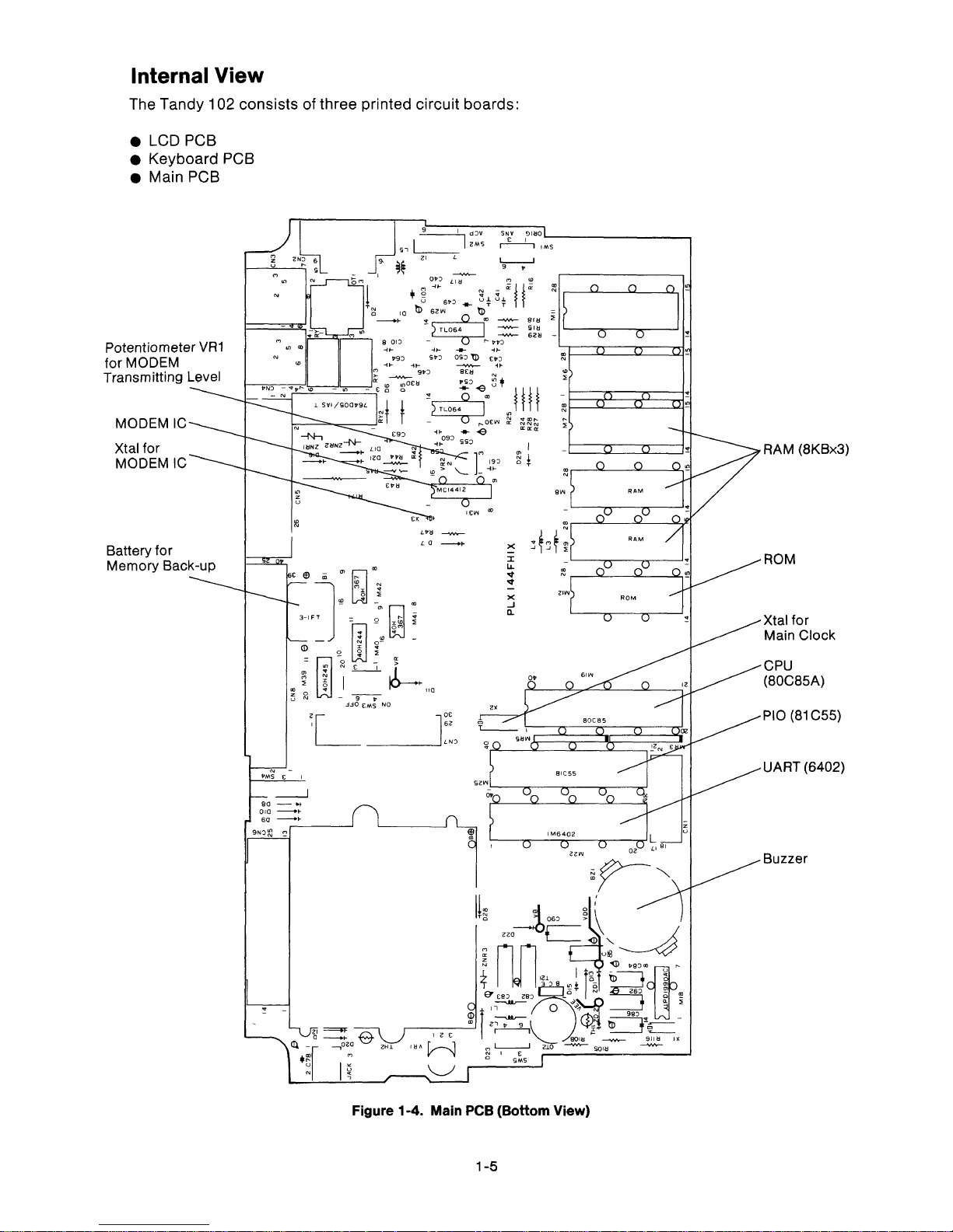
Internal View
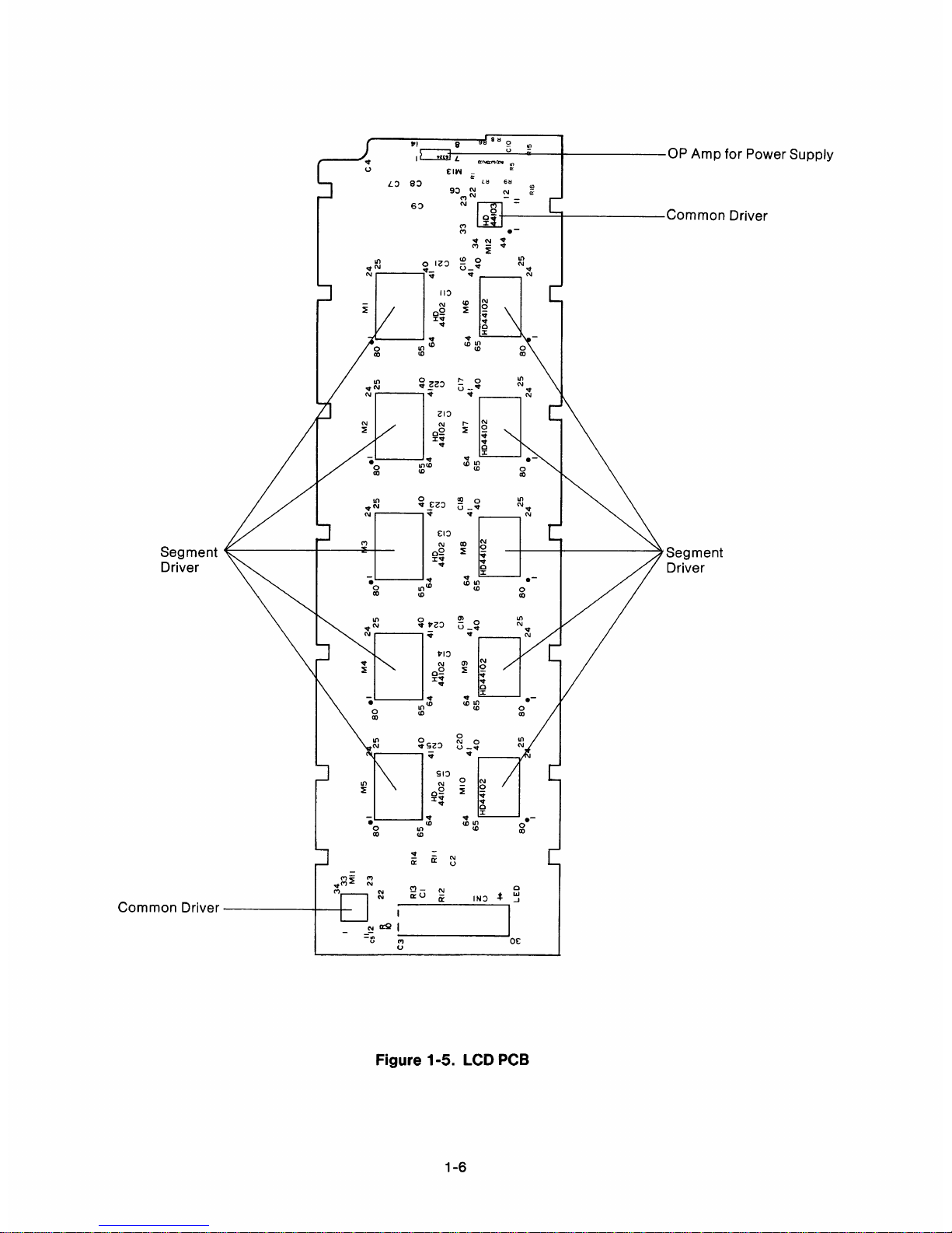
The Tandy 102 consists of three printed circuit boards:
• LCD PCB
• Keyboard PCB
• Main PCB
d0V SNV 0180
E
aSSI
L
ZMS
r --
I
IMS
9• /
ZI L
L
9
ODO
L18
c m
N N
Potentiometer VR1
for MODEM
Transmitting Level
MODEM IC
Xtal for
MODEM IC
10
b 6001
°T
V V 1 U
6110
f
1
T
T
+F o - %,V SIN
-w SIN
608
8010 - V
r ssZ
-IF dl- t _4F
£q0
aV90
540 050
YD
iF -4F vw- iF
980 8£a m
q S0
9N0 oqr
m
Battery for
I
Memory Back-up
9N3N rt
Zx
° RAM (8KBx3)
RAM
HUM
1
N
X
2119
ROM
J
a
09
5815
f
801 RAM
6119
8OC85
IZN
8IC55
e
I M6402
ZZ19
Figure 1-4. Main PCB (Bottom View)
0C8
u T
£ o
o
i-
1 SVI/500V9L
T
-
C90
I-
09D
IANZ 2850
L10
a
F
100 qqa ¢
190 o
Z
U
ID
CON
Ex
01
co
r0£W
a
Ss0
m
m r
!7
7
m
m
m r'7
MC14412
CO --pp
3-IFT = ° r a
a
m
_
m
a
ci
N N £ I
>
m
v
f
o
I
4-
Z ° 11
4
9 V
dd0
EMS NO
L
0Z
_1131
1Z
CIE
z
Xtal for
Main Clock
CPU
(80C85A)
PIO (81 C55)
UART (6402)
Buzzer
1-5
vgm<fmm3
34
33
Mil
23
22
3
24 •1 M2 24
25 80 25 80
65
64
24
C4
25
r
u
J
R13 R14
Cl
M5 M4
24
80.1 25 80
• I 25 80.1
65
RI1 64 HD
R12 44102
T
C2
64
MI0
65
u
HD44102
u
q LED
80
•
40 65 40 65
4I
c%j
64 HD 4I 64
HD
u 44102
a u 44102 D
u u
u
C20 C19
41
40
64
M9
65
HD44102
25 80
•
41
40
24
25
64
M8
65
HD44102
80
•
40 65 40
41- 64 HD 41N
C14
44102
Nuu
C18
41
40
64
M7
65
HD44102
C17
41
40
25
24
80
•
24
25
MI
44102
u
64
M6
65
HD44102
80
40
41
C16 33 23
a)
u u
v y r ro
4140 34
22
R,
M12
HD
10
44
•
12
.
Rs
CIO
25
I II
24
RL6
15
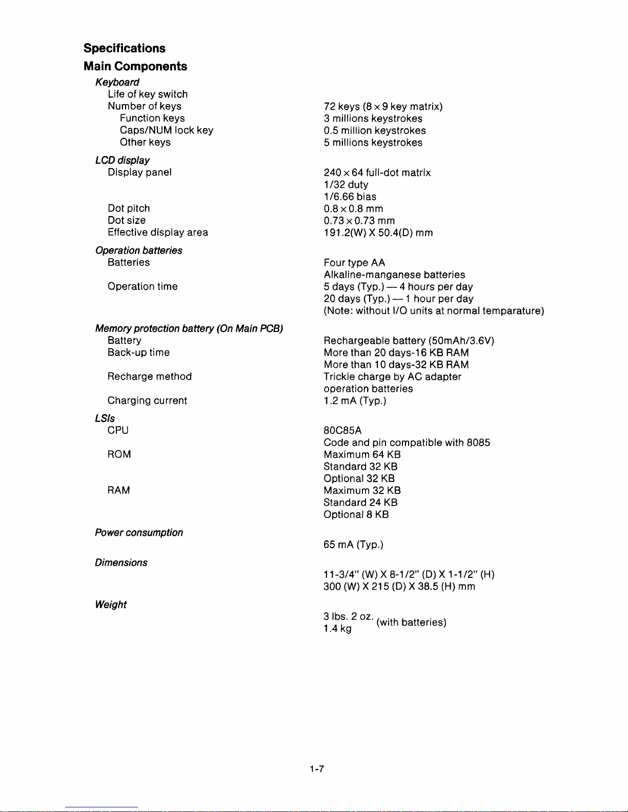
Specifications
Main Components
Keyboard
Life of key switch
Number of keys
Function keys
Caps/NUM lock key
Other keys
LCD display
Display panel
Dot pitch
Dot size
Effective display area
Operation batteries
Batteries
Operation time
Memory protection battery (On Main PCB)
Battery
Back-up time
Recharge method
Charging current
LSIs
CPU
ROM
RAM
Power consumption
Dimensions
Weight
72 keys (8 x 9 key matrix)
3 millions keystrokes
0.5 million keystrokes
5 millions keystrokes
240 x 64 full-dot matrix
1/32 duty
1/6.66 bias
0.8 x 0.8 mm
0.73x0.73 mm
191.2(W) X 50.4(D) mm
Four type AA
Alkaline-manganese batteries
5 days (Typ.) - 4 hours per day
20 days (Typ.) - 1 hour per day
(Note: without I/O units at normal temparature)
Rechargeable battery (50mAh/3.6V)
More than 20 days-16 KB RAM
More than 10 days-32 KB RAM
Trickle charge by AC adapter
operation batteries
1.2 mA (Typ.)
80C85A
Code and pin compatible with 8085
Maximum 64 KB
Standard 32 KB
Optional 32 KB
Maximum 32 KB
Standard 24 KB
Optional 8 KB
65 mA (Typ.)
11-3/4" (W) X 8-1/2" (D) X 1-1 /2" (H)
300 (W) X 215 (D) X 38.5 (H) mm
3 lbs. 2 oz.
(with batteries)
1.4 kg
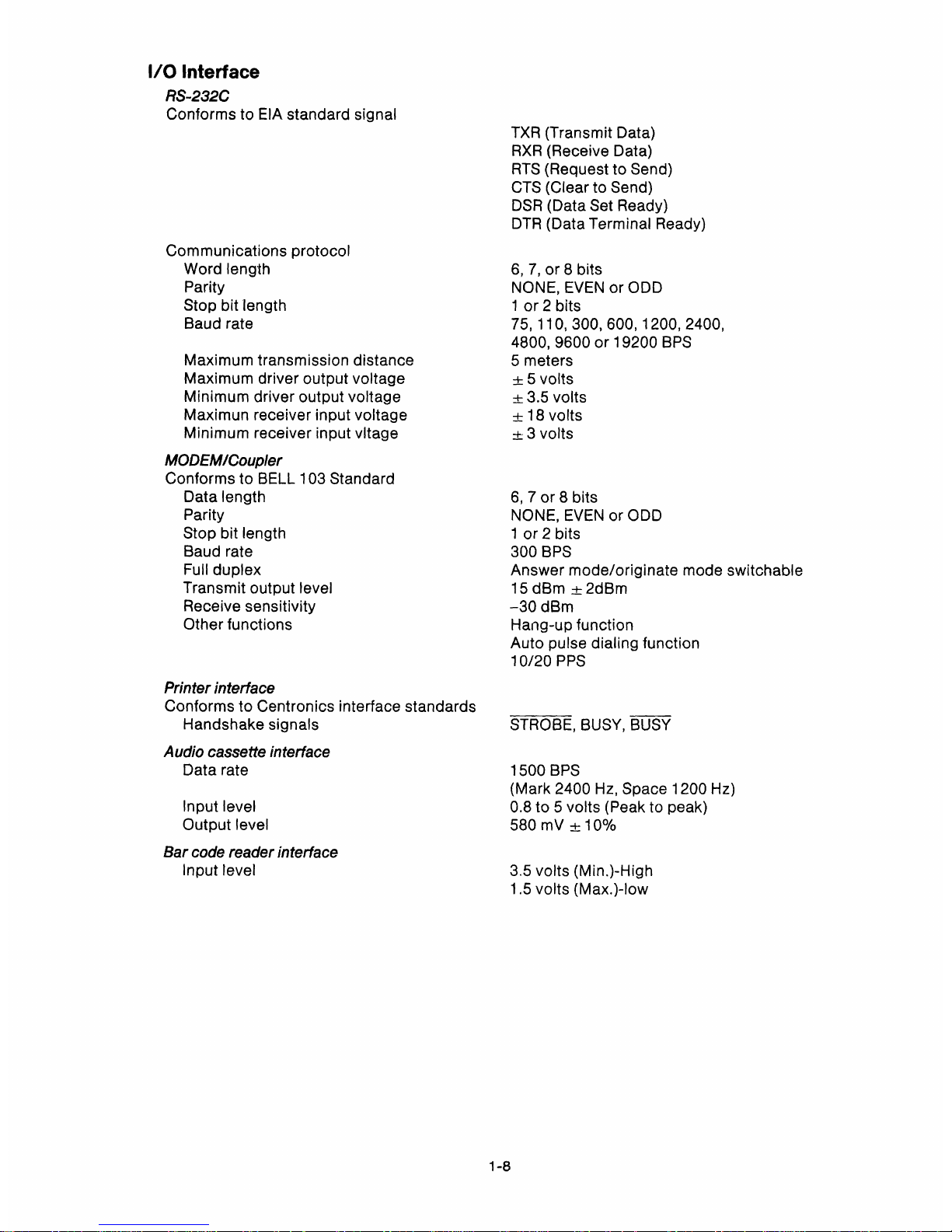
I/O Interface
RS-232C
Conforms to EIA standard signal
Communications protocol
Word length
Parity
Stop bit length
Baud rate
Maximum transmission distance
Maximum driver output voltage
Minimum driver output voltage
Maximun receiver input voltage
Minimum receiver input vltage
MODEMICoupler
Conforms to BELL 103 Standard
Data length
Parity
Stop bit length
Baud rate
Full duplex
Transmit output level
Receive sensitivity
Other functions
Printer interface
Conforms to Centronics interface standards
Handshake signals
Audio cassette interface
Data rate
Input level
Output level
Bar code reader interface
Input level
TXR (Transmit Data)
RXR (Receive Data)
RTS (Request to Send)
CTS (Clear to Send)
DSR (Data Set Ready)
DTR (Data Terminal Ready)
6, 7, or 8 bits
NONE, EVEN or ODD
1 or 2 bits
75, 110, 300, 600, 1200, 2400,
4800, 9600 or 19200 BPS
5 meters
± 5 volts
±
3.5 volts
± 18 volts
± 3 volts
6, 7 or 8 bits
NONE, EVEN or ODD
1 or 2 bits
300 BPS
Answer mode/originate mode switchable
15 dBm ± 2dBm
-30 dBm
Hang-up function
Auto pulse dialing function
10/20 PPS
STROBE, BUSY, BUSY
1500 BPS
(Mark 2400 Hz, Space 1200 Hz)
0.8 to 5 volts (Peak to peak)
580 mV ± 10%
3.5 volts (Min.)-High
1.5 volts (Max.)-low
II. DISASSEMBLY INSTRUCTIONS
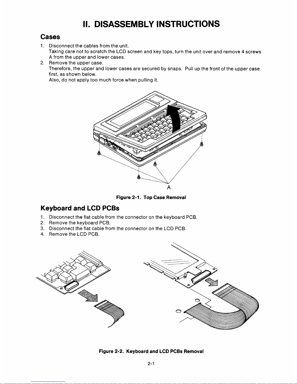
Cases
1. Disconnect the cables from the unit.
Taking care not to scratch the LCD screen and key tops, turn the unit over and remove 4 screws
A from the upper and lower cases.
2. Remove the upper case.
Therefore, the upper and lower cases are secured by snaps. Pull up the front of the upper case
first, as shown below.
Also, do not apply too much force when pulling it.
A
Figure 2-1. Top Case Removal
Keyboard and LCD PCBs
1. Disconnect the flat cable from the connector on the keyboard PCB.
2. Remove the keyboard PCB.
3. Disconnect the flat cable from the connector on the LCD PCB.
4. Remove the LCD PCB.
V
V
1 I
1
e
C5
Figure 2-2. Keyboard and LCD PCBs Removal
2-1
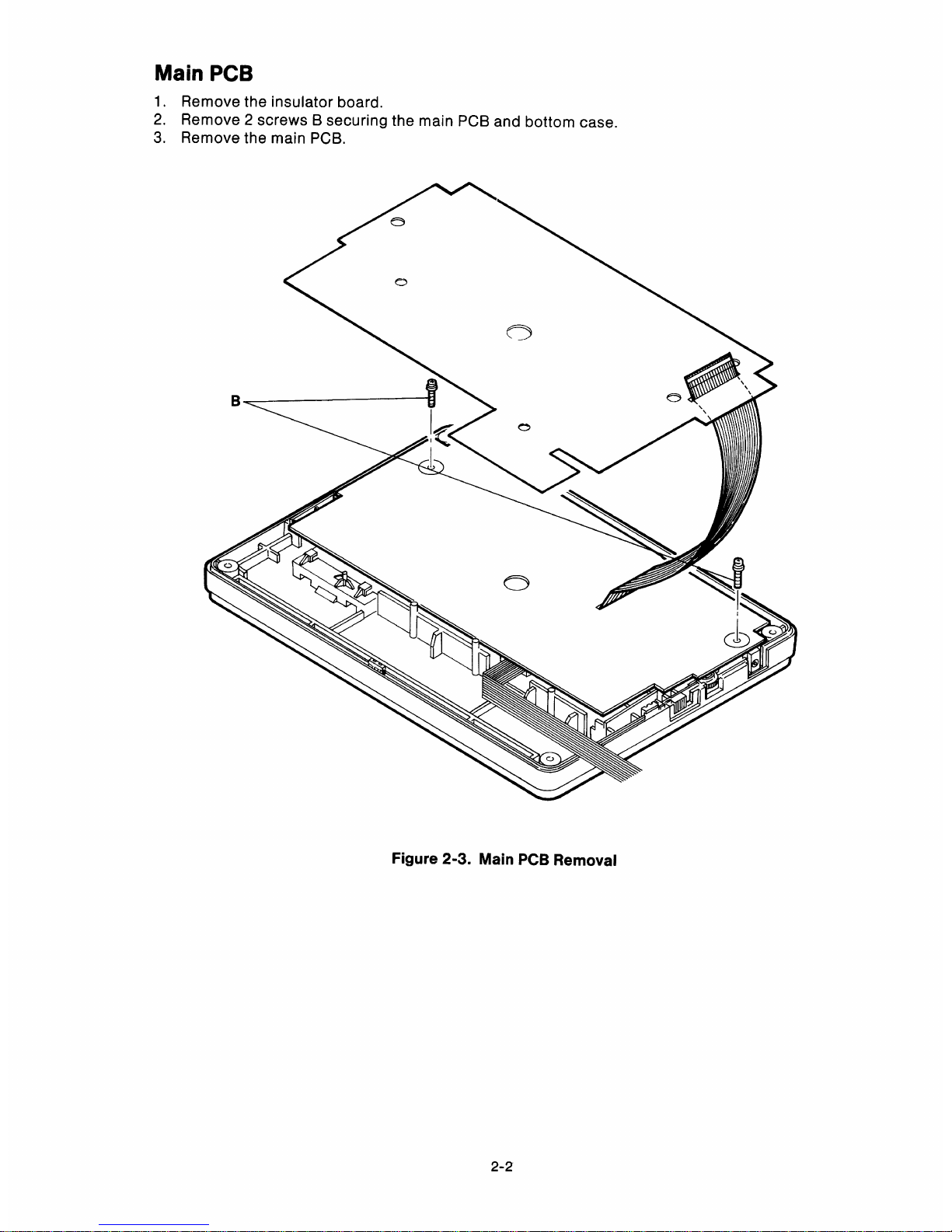
Main PCB
1. Remove the insulator board.
2. Remove 2 screws B securing the main PCB and bottom case.
3. Remove the main PCB.
B
U
0
C)
CD
U
Figure 2-3. Main PCB Removal
III. MAINTENANCE
To Clean the Body and LCD Display
1. To avoid operational trouble, always keep the Tandy 102 clean.
2. Clean the body and the LCD screen using a soft, dry, lint-free cloth.
3. For tough stains, clean the body or the LCD screen with benzol.
Caution: Do not use any solvents other than benzol.

á
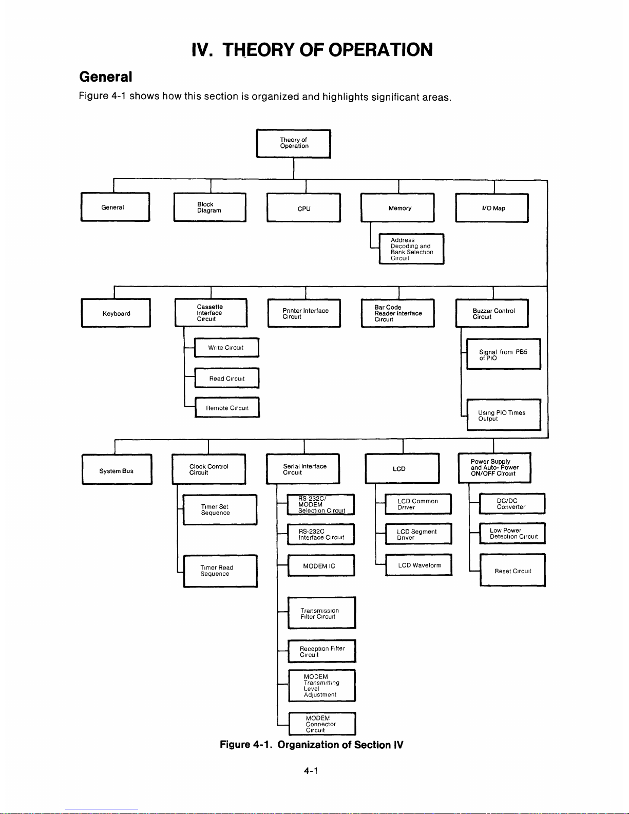
IV. THEORY OF OPERATION
General
Figure 4-1 shows how this section is organized and highlights significant areas.
Theory of
Operation
General
Block
Diagram
CPU I 1
Memory
Address
Decoding and
Bank Selection
Circuit
Keyboard
System Bus
Cassette
Interface
Circuit
11
Read Circuit
Remote Circuit
Clock Control
Circuit
Timer Set
Sequence
Timer Read
Sequence
Printer Interface
Circuit
Serial Interface
Circuit
Bar Code
Reader Interface
Circuit
LCD
fRS-232C/
LCD Common
MODEM
Driver
Selection Circuit
RS-232C LCD Segment
Interface Circuit Driver
MODEM IC LCD Waveform
Transmission
Filter Circuit
Reception Filter
Circuit
MODEM
Transmitting
Level
Adjustment
y
MODEM
Connector
Circuit
Figure 4-1. Organization of Section IV
I
1
I/O Map
Buzzer Control
Circuit
Signal from PB5
of PIO
Using PIO Times
Output
Power Supply
and Auto- Power
ON/OFF Circuit
DC/DC
Converter
Low Power
Detection Circuit
Reset Circuit
4-1
Block Diagram
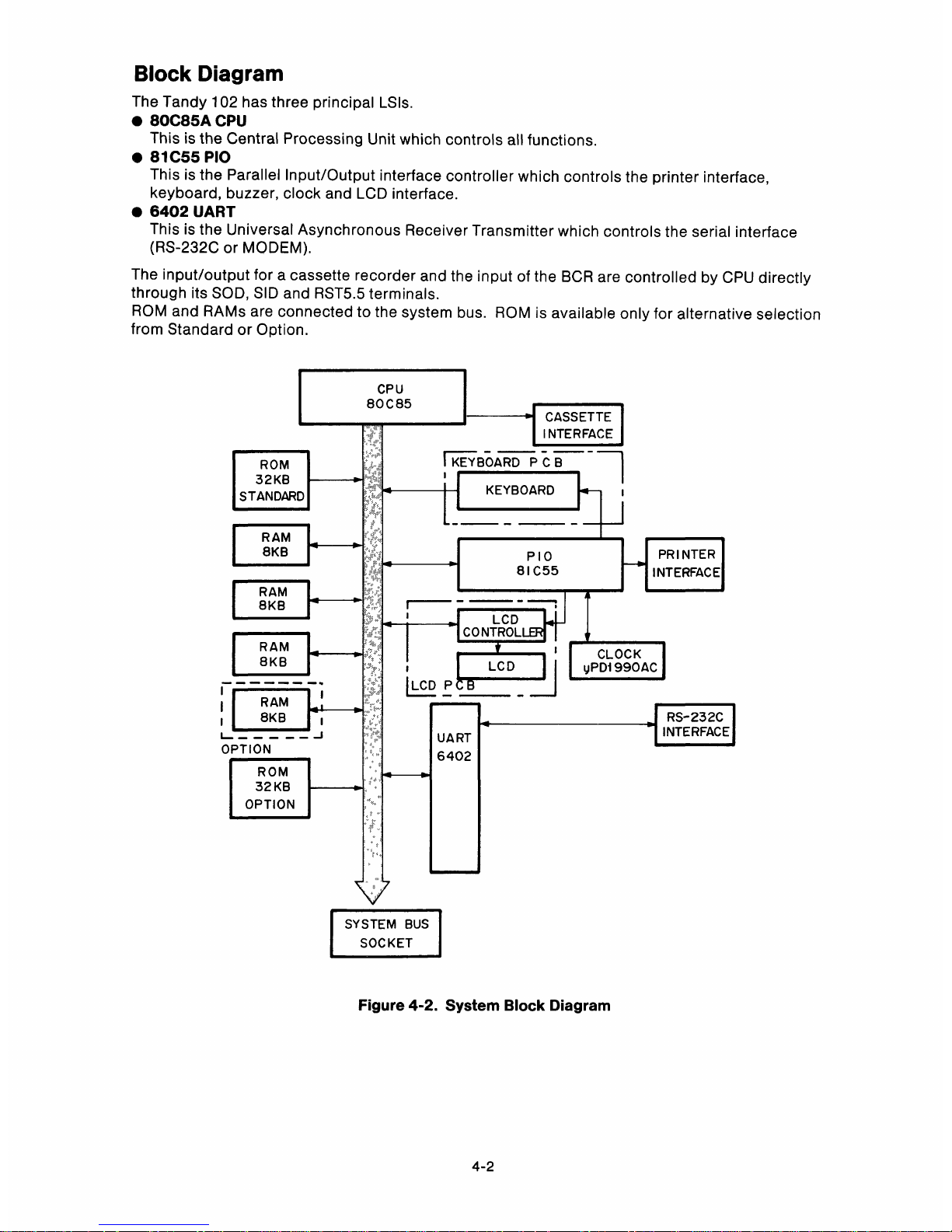
The Tandy 102 has three principal LSIs.
• 8OC85A CPU
This is the Central Processing Unit which controls all functions.
• 81 C55 PIO
This is the Parallel Input/Output interface controller which controls the printer interface,
keyboard, buzzer, clock and LCD interface.
• 6402 UART
This is the Universal Asynchronous Receiver Transmitter which controls the serial interface
(RS-232C or MODEM).
The input/output for a cassette recorder and the input of the BCR are controlled by CPU directly
through its SOD, SID and RST5.5 terminals.
ROM and RAMs are connected to the system bus. ROM is available only for alternative selection
from Standard or Option.
CPU
8OC85
CASSETTE
INTERFACE
ROM
32KB
STANDARD
RAM
8KB
FKEYBOARD PC B
I
KEYBOARD i
PIO
PRINTER
81 C55
INTERFACE
RAM
8KB
RAM
8KB
I
i
LCD
CONTROL
I I
I RAM
8KB
OPTION
ROM
32KB
OPTION
LCD P
U A RT
6402
SYSTEM BUS
SOCKET
Figure 4-2. System Block Diagram
CLOCK
LCD yPD1990AC
RS-232C
INTERFACE
CPU
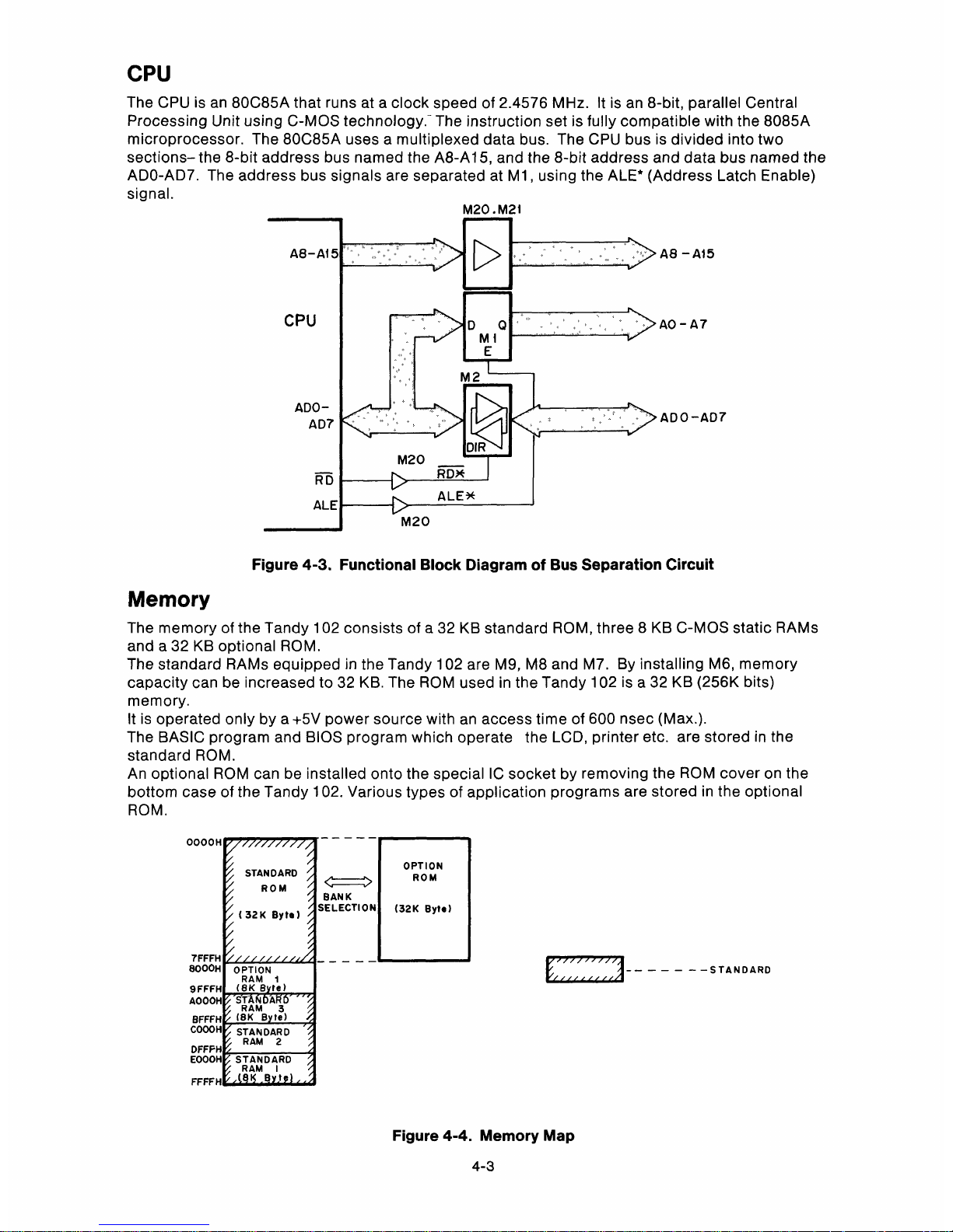
The CPU is an 80C85A that runs at a clock speed of 2.4576 MHz. It is an 8-bit, parallel Central
Processing Unit using C-MOS technology.- The instruction set is fully compatible with the 8085A
microprocessor. The 80C85A uses a multiplexed data bus. The CPU bus is divided into two
sections- the 8-bit address bus named the A8-A1 5, and the 8-bit address and data bus named the
ADO-AD7. The address bus signals are separated at M1, using the ALE* (Address Latch Enable)
signal.
M20.M21
CPU
A8-415 ",
M2
ADO-
AD7
RD
ALE
M20
RDA
ALEX
AS -A15
A0-A7
ADO-AD7
M20
Figure 4-3. Functional Block Diagram of Bus Separation Circuit
Memory
The memory of the Tandy 102 consists of a 32 KB standard ROM, three 8 KB C-MOS static RAMs
and a 32 KB optional ROM.
The standard RAMs equipped in the Tandy 102 are M9, M8 and M7. By installing M6, memory
capacity can be increased to 32 KB. The ROM used in the Tandy 102 is a 32 KB (256K bits)
memory.
It is operated only by a +5V power source with an access time of 600 nsec (Max.).
The BASIC program and BIOS program which operate the LCD, printer etc. are stored in the
standard ROM.
An optional ROM can be installed onto the special IC socket by removing the ROM cover on the
bottom case of the Tandy 102. Various types of application programs are stored in the optional
ROM.
0000H
( 32K Byte)
STANDARD
ROM
7FFFH
8000H
OPTION
RAM I
9FFFH ( 8K B te)
AOOOH ST A
RAM 3
BFFFH
(SK B to)
COOOH
STANDARD
DFFFH
RAM 2
E000H STANDARD
RAM I
FFFFH
K
B t
Figure 4-4. Memory Map
OPTION
BAN K
SELECTION (32K Byte)
-- - - - - -STANDARD
4-3
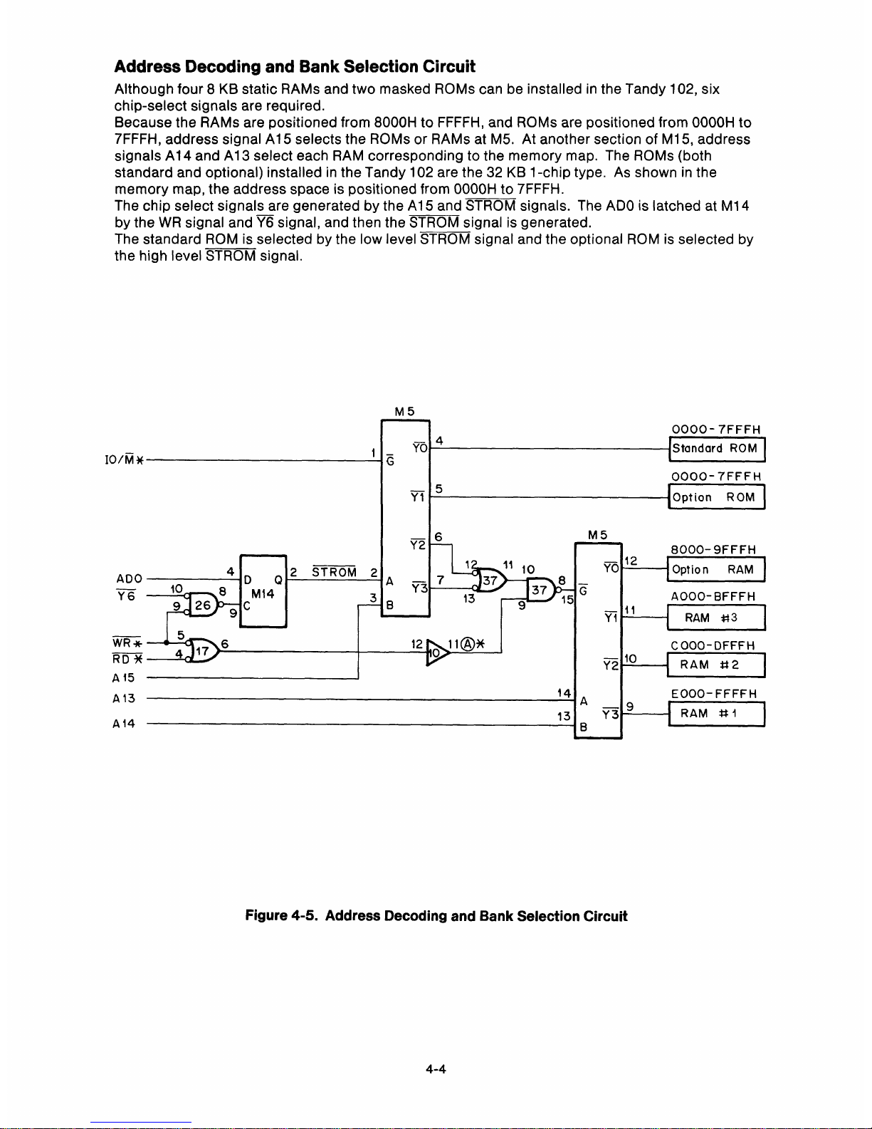
Address Decoding and Bank Selection Circuit
Although four 8 KB static RAMs and two masked ROMs can be installed in the Tandy 102, six
chip-select signals are required.
Because the RAMs are positioned from 8000H to FFFFH, and ROMs are positioned from OOOOH to
7FFFH, address signal Al 5 selects the ROMs or RAMs at M5. At another section of M15, address
signals Al 4 and A13 select each RAM corresponding to the memory map. The ROMs (both
standard and optional) installed in the Tandy 102 are the 32 KB 1-chip type. As shown in the
memory map, the address space is positioned from OOOOH to 7FFFH.
The chip select signals are generated by the A15 and STROM signals. The ADO is latched at M14
by the WR signal and Y6 signal, and then the STROM signal is generated.
The standard ROM is selected by the low level STROM signal and the optional ROM is selected by
the high level STROM signal.
M5
TO 4
Y1 5
Y2 6
M5
0000-7FFFH
Standard ROM
0000-7FFFH
Option ROM
8000-9FFFH
ADO
4 D Q
2 STROM 2 A
7
Y6 10
8
M14
3
Y3
9 26 9 C 8
WR*
RDXE
A15
A13
A14
5 6
4 17
1 11
10 TO 12 Option RAM
13
37
37
85
G
9
Y1 11
12 0 11 A0#
A000-BFFFH
RAM # 3
0000-DFFFH
Y2 10
RAM #2
14 A
13
Y3
9
8
E000-FFFFH
RAM #1
Figure 4-5. Address Decoding and Bank Selection Circuit
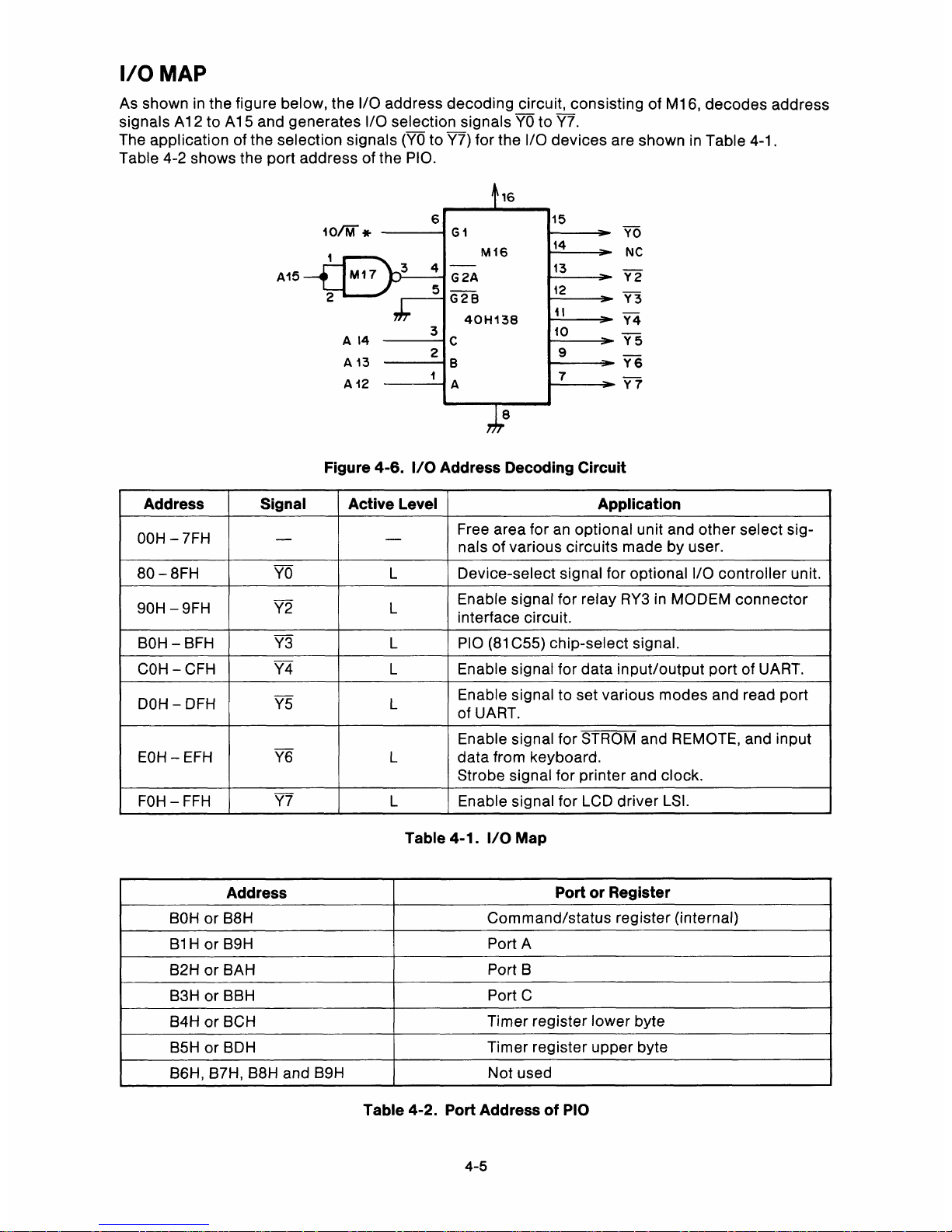
I/O MAP
As shown in the figure below, the I/O address decoding circuit, consisting of M16, decodes address
signals A12 to Al 5 and generates I/O selection signals YO to Y7.
The application of the selection signals (YO to Y7) for the I/O devices are shown in Table 4-1.
Table 4-2 shows the port address of the PIO.
16
6
15
10f
G1
14
YO
1
M16
NC
3 4 13
A15
M17
G 2A
Y2
5
12
2
G2B Y3
40H138
1I
Y4
3 10
A 14
C
Y5
2
9
A13
B
Y6
7
A 12
A Y7
8
Figure 4-6. I/O Address Decoding Circuit
Address
Signal
Active Level Application
Free area for an optional unit and other select sig-
OOH - 7FH -
nals of various circuits made by user.
80 - 8FH YO L Device-select signal for optional I/O controller unit.
Enable signal for relay RY3 in MODEM connector
90H - 9FH Y2
L
interface circuit.
BOH - BFH
Y3
L PIO (81 C55) chip-select signal.
COH - CFH Y4 L Enable signal for data input/output port of UART.
Enable signal to set various modes and read port
DOH - DFH Y5 L
of UART.
Enable signal for STROM and REMOTE, and input
EOH - EFH
Y6
L data from keyboard.
Strobe signal for printer and clock.
FOH - FFH Y7
L
Enable signal for LCD driver LSI.
Table 4-1. I/O Map
Address
BOH or B8H
B1 H or B9H
82H or BAH
B3H or BBH
B4H or BCH
B5H or BDH
B6H, B7H, B8H and B9H
Port or Register
Command/status register (internal)
Port A
Port B
Port C
Timer register lower byte
Timer register upper byte
Not used
Table 4-2. Port Address of PIO
4-5
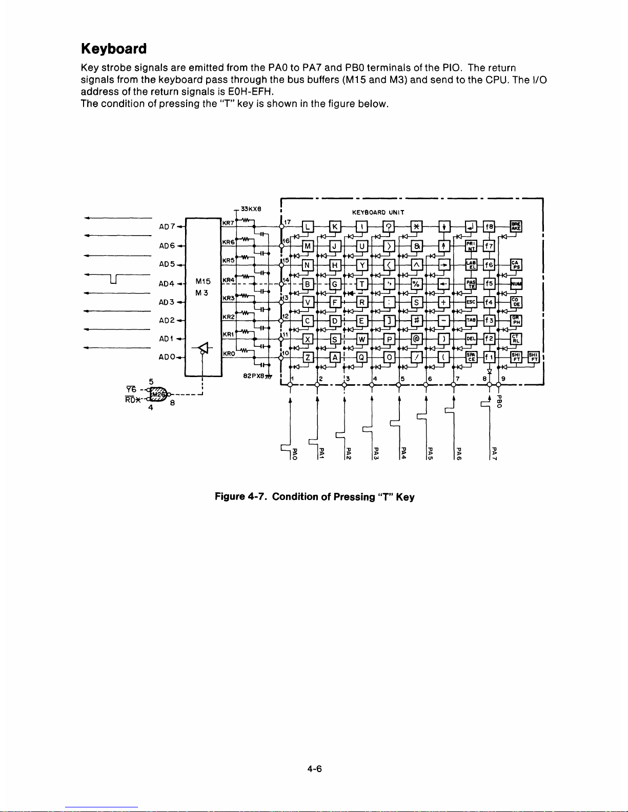
Keyboard
Key strobe signals are emitted from the PAO to PA7 and PBO terminals of the PIO. The return
signals from the keyboard pass through the bus buffers (Ml 5 and M3) and send to the CPU. The I/O
address of the return signals is EOH-EFH.
The condition of pressing the "T" key is shown in the figure below.
33KX8
KR7
17
AD7
L
AD IS
KR6
16
M
AD 5
KR5
15
N
AD4
M15
KR4 - -
--
- 14
- B
M3
AD3
KR3
43
V
A02
KR2
12
C
AD 1
KR1 11
x
KRO
110
ADO
Z
82PXB
K
KEYBOARD UNIT
J U >
H Y
D I E ]
s
A I
W P
Q
0
f8
WRE
ME
a 4
PRI
T
f7
A -e
t
EL
P
E
f6
f5
PS
S +
4
ESC
TAB
f4
f3
co
DE
PH
n4
DEL
f2
RL
/
(
SFA
C E
f1
SHI
FT
2 13 4 5 6 7 8 9
CD
0
D . D D D D D
0 N W A
O W -
Figure 4-7. Condition of Pressing "T" Key
SHI
FT
J
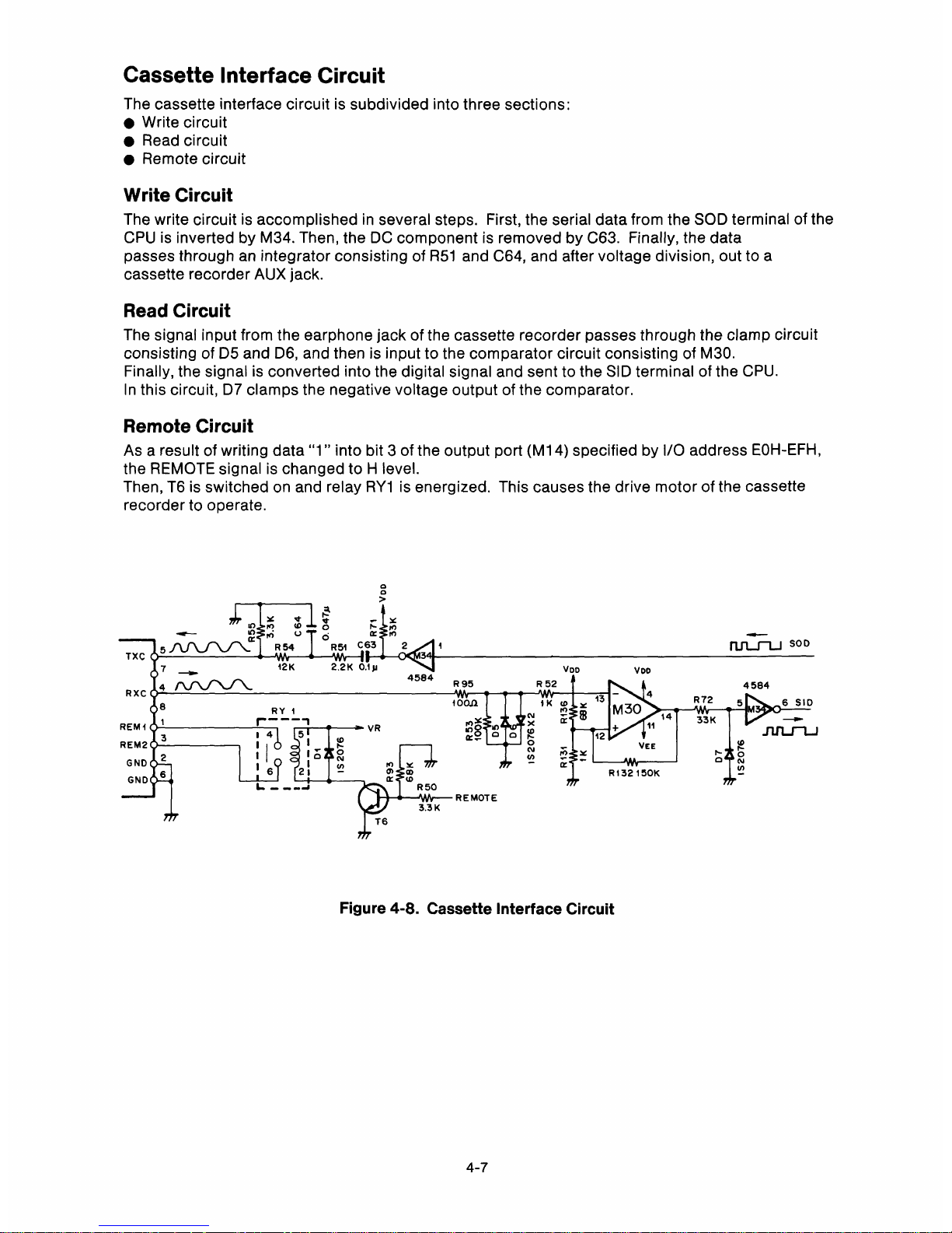
Cassette Interface Circuit
The cassette interface circuit is subdivided into three sections:
• Write circuit
• Read circuit
• Remote circuit
Write Circuit
The write circuit is accomplished in several steps. First, the serial data from the SOD terminal of the
CPU is inverted by M34. Then, the DC component is removed by C63. Finally, the data
passes through an integrator consisting of R51 and C64, and after voltage division, out to a
cassette recorder AUX jack.
Read Circuit
The signal input from the earphone jack of the cassette recorder passes through the clamp circuit
consisting of D5 and D6, and then is input to the comparator circuit consisting of M30.
Finally, the signal is converted into the digital signal and sent to the SID terminal of the CPU.
In this circuit, D7 clamps the negative voltage output of the comparator.
Remote Circuit
As a result of writing data "1" into bit 3 of the output port (Ml 4) specified by I/O address EOH-EFH,
the REMOTE signal is changed to H level.
Then, T6 is switched on and relay RY1 is energized. This causes the drive motor of the cassette
recorder to operate.
0
0
TXC
Y. It
IS) M t0
E-- ,n U
C
D: M
5
R54 R51
C63 2 1
pj j 1j SOD
3
7
12K 2 .2K 0.1p
VDD VDD
4584
R95 R52
4584
RXC
4
8
RY 1
10012 1 K
M
13
M30
4
R72
5 6 SID
REMi
r'---1
VR )X
,n
x
+ 14 33K -
p 11
1 4 5
08
C 0
ti 12
L
REM2
3
I I ( 1-
0 so
I
I p'
N Y VEE
2
0
M
t_ 0
GND 1 I
N
M Y
N
D N
GND 6
6 21
a)
R132150K
L. _ --- .j R50
T6
3.3 K
REMOTE
Figure 4-8. Cassette Interface Circuit
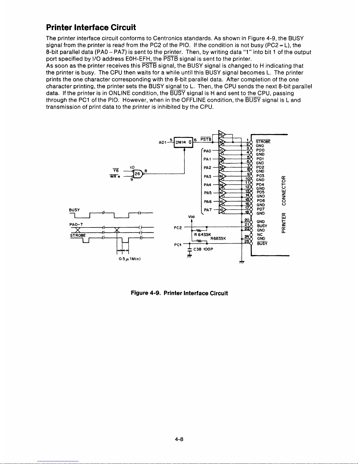
Printer Interface Circuit
The printer interface circuit conforms to Centronics standards. As shown in Figure 4-9, the BUSY
signal from the printer is read from the PC2 of the PIO. If the condition is not busy (PC2 = L), the
8-bit parallel data (PAO - PA7) is sent to the printer. Then, by writing data "1 " into bit 1 of the output
port specified by I/O address EOH-EFH, the PSTB signal is sent to the printer.
As soon as the printer receives this PSTB signal, the BUSY signal is changed to H indicating that
the printer is busy. The CPU then waits for a while until this BUSY signal becomes L. The printer
prints the one character corresponding with the 8-bit parallel data. After completion of the one
character printing, the printer sets the BUSY signal to L. Then, the CPU sends the next 8-bit parallel
data. If the printer is in ONLINE condition, the BUSY signal is H and sent to the CPU, passing
through the PC1 of the PIO. However, when in the OFFLINE condition, the BUSY signal is L and
transmission of print data to the printer is inhibited by the CPU.
PSTB
AD1 5 DM14
Q
6
1
STROBE
GND
PAO
PA 1
0
3
A
PDO
GND
PD1
6
GND
10
PA 2
3
PD2
Y6
26
8
8
GND
9
WR PA3
32
P03
0:
9
PA4
PA 5
10
GND
0
12
PD4
GND
U
PD5
W
Z
# GND
z
PA 6
10
PD6 0
16
GND
U
BUSY
PA 7
10
1 PD7
VDD
GND
0:
W
20
GND
i^
PAO-7 21
BUSY
Z_
5-
PC2
GND
0
STROBE
R 6433K
_
24
NC
R6833K GND
PCI
BUSY
0.5 A (Min)
C38 100P
Ill
Figure 4-9. Printer Interface Circuit

Bar Code Reader Interface Circuit
The input signal from the bar code reader is subjected to waveform shaping, inverted by the
Schmitt-type inverter (M34), and then sent to the PC3 terminal of the PIO and the RST5.5 terminal of
the CPU.
When the bar code reader reads the first white part of the bar code, a L level signal is generated,
then inverted by M34 to notify the CPU of an interruption. As soon as RST5.5 interruption occurs,
the CPU starts the data input operation, passing through the PC3 of the PIO. As the bar code
reader is moved across the bars, H and L signals (which correspond to the white and black bars,
respectively) are generated continuously and inversion signals are sent to the PC3 of the PIO as the
serial input data stream.
BLACK LINE
WHITE LINE
VDD
BLACK LINE
WHITE LINE
CNI
Y
0
M
ti
Q:
M
I
RXD
2
13
M
12
BCR
( 8IC55-PC3)
9
VDD
Voo
RST5.5
GND
5
NC
(CPU)
GND
7
1
3
6
NC
4
8
Figure 4-10. Bar Code Reader Interface Circuit

Buzzer Control Circuit
There are two ways to operate the buzzer. One is to sound the buzzer with the specified frequency
by emitting signals from the PB5 of the PIO and the other, by using the timer output signal of the
PIO.
Signal from PB5 of PIO
When the PB2 of the PIO is H, the buzzer sounds by repeated switching of the buzzer driving
transistor. This is caused by H, L, H, L ... output signals from the PB5 synchronizing with the
frequency for sounding the buzzer. This method is used for the BEEP command in BASIC.
PIO Timer Output
In this method, the buzzer is sounded by setting the PIO timer in the square wave output mode. To
write the value corresponding to the sound frequency, the CPU assigns B4H, B5H, BCH or BDH to
the I/O port address. This frequency is assigned by the first parameter of the SOUND command in
BASIC.
If the above procedures are completed, the TO terminal of the PIO outputs the square waves, and
the P62 of the PIO controls the length of the sound whenever the PB5 is "L". How long the sound is
heard depends on the second parameter of SOUND command in BASIC.
VDD
R4
BUZZER
PB5
M25
VDD
P10
PB2
31
TO
6
R3
33K
33K
R61
33K
12
11
13
M26
R2
33K
T1
2 SA
1162
R113
3.3 K
V EE
Figure 4-11. Buzzer Control Circuit
oa
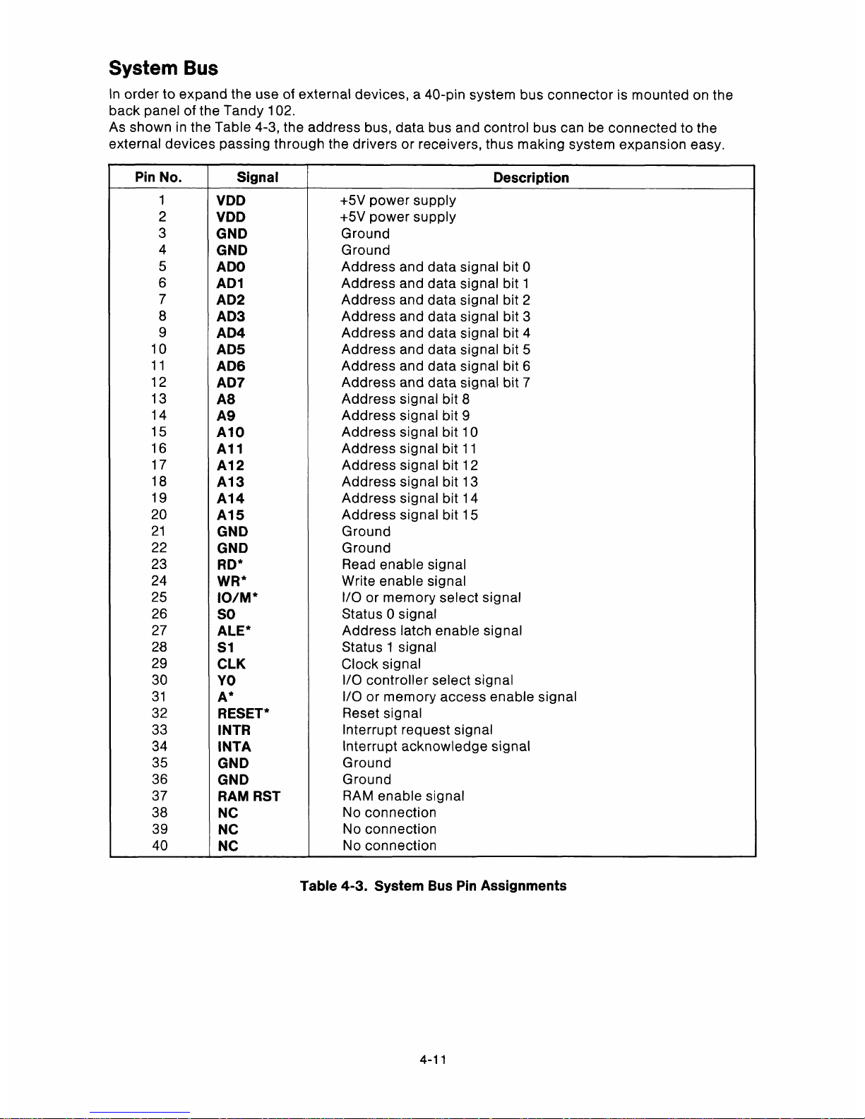
System Bus
In order to expand the use of external devices, a 40-pin system bus connector is mounted on the
back panel of the Tandy 102.
As shown in the Table 4-3, the address bus, data bus and control bus can be connected to the
external devices passing through the drivers or receivers, thus making system expansion easy.
Pin No.
Signal
Description
1
VDD
+5V power supply
2
VDD
+5V power supply
3
GND
Ground
4
GND
Ground
5
ADO
Address and data signal bit 0
6
AD1
Address and data signal bit 1
7
AD2
Address and data signal bit 2
8
AD3
Address and data signal bit 3
9
AD4
Address and data signal bit 4
10
AD5
Address and data signal bit 5
11
AD6
Address and data signal bit 6
12
AD7
Address and data signal bit 7
13
A8
Address signal bit 8
14
A9
Address signal bit 9
15
A10
Address signal bit 10
16
All
Address signal bit 11
17
A12
Address signal bit 12
18
A13
Address signal bit 13
19
A14
Address signal bit 14
20
A15
Address signal bit 15
21
GND
Ground
22
GND
Ground
23
RD*
Read enable signal
24
WR*
Write enable signal
25
10/M *
I/O or memory select signal
26
SO
Status 0 signal
27
ALE*
Address latch enable signal
28
Si
Status 1 signal
29
CLK Clock signal
30
YO
I/O controller select signal
31
A*
I/O or memory access enable signal
32
RESET*
Reset signal
33
INTR
Interrupt request signal
34
INTA
Interrupt acknowledge signal
35
GND
Ground
36
GND
Ground
37
RAM RST
RAM enable signal
38
NC
No connection
39
NC
No connection
40
NC
No connection
Table 4-3. System Bus Pin Assignments
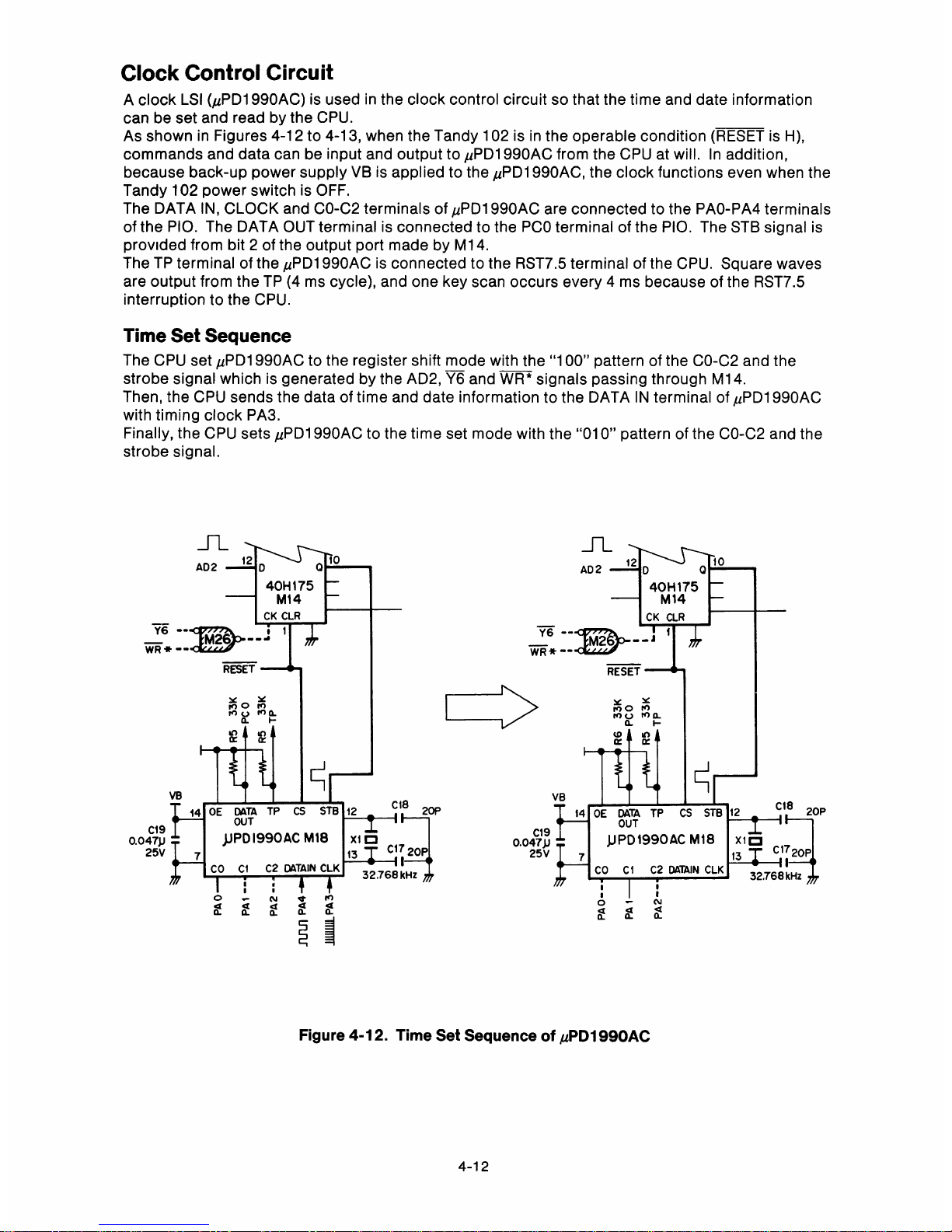
Clock Control Circuit
A clock LSI (4PD1990AC) is used in the clock control circuit so that the time and date information
can be set and read by the CPU.
As shown in Figures 4-12 to 4-13, when the Tandy 102 is in the operable condition (RESET is H),
commands and data can be input and output to,uPD1990AC from the CPU at will. In addition,
because back-up power supply VB is applied to theuPD1990AC, the clock functions even when the
Tandy 102 power switch is OFF.
The DATA IN, CLOCK and C0-C2 terminals ofpPD1990AC are connected to the PAO-PA4 terminals
of the PIO. The DATA OUT terminal is connected to the PCO terminal of the PIO. The STB signal is
provided from bit 2 of the output port made by M14.
The TP terminal of the ,uPD1990AC is connected to the RST7.5 terminal of the CPU. Square waves
are output from the TP (4 ms cycle), and one key scan occurs every 4 ms because of the RST7.5
interruption to the CPU.
Time Set Sequence
The CPU set 4uPD1990AC to the register shift mode with the "100" pattern of the C0-C2 and the
strobe signal which is generated by the AD2, Y6 and WR* signals passing through M14.
Then, the CPU sends the data of time and date information to the DATA IN terminal of,uPD1990AC
with timing clock PA3.
Finally, the CPU sets APD1990AC to the time set mode with the "010" pattern of the C0-C2 and the
strobe signal.
120 010
Y6 -
WR* -
M26
_FL
AD 2
40H 175
40H175
M14 M14
CK CLR
CK CLR
-- 1
Y6
MZ J
WR*--
0
RESET
MU
rna
a.
RESET
gr
C19
0.047J1
25V
VB VB
T
TP CS STB 12
cis
20P
14 OE TP CS STB 12
cis
20P
T
14 OE
O
T
O
U
7
JJPD I990AC M18 xi c3
13
C17
20P
32.768 kHz
1 i
O N V M
a a a a a
CO C1 C2 DATAIN CLK
11
O.047;,
JJPD1990AC M18 xi c3
25V
7
120 0
10
Y
MU Ma
i-
a.
CO C 1 C2 DATAIN CLK
1 1
t 1
O Cu
a a a
C1
20P
13
32.768 kHz
Figure 4-12. Time Set Sequence of ,uPD1990AC
 Loading...