

Tandy CM-8, 26-3215 Service Manual

TANDY®
\ .
erv1ce
Color
Monitor
CM-8
for
Color
Computer
3
Catalog
Number
:
26-3215
CUSTOM
MANUFACTURED
FOR
RADIO
SHACK, A DIVISION
OF
TANDY
CORPORATION
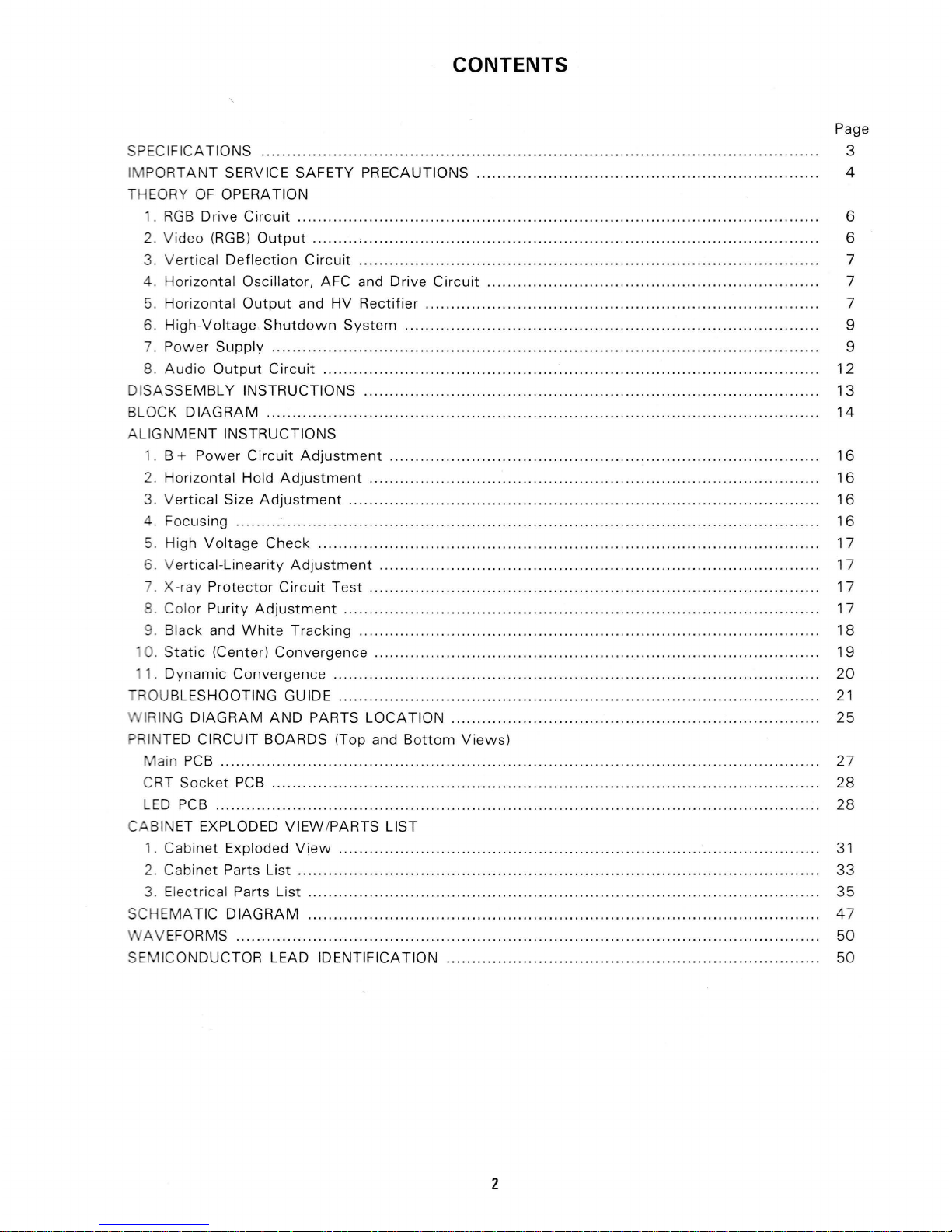
CONTENTS
Page
SPECIFICATIONS
..
. . . . . ... . .... .... .. .... ..
....... ..... ... . . . ... . ... . .
..
. . ....
....... ..
. .
....
. .... .. .. . . ... . .
..
. . . .
..
..... ... 3
I
POR
TANT
SERVICE SAFETY PRECAUTIONS ......... ...... .
......
.......
....
....
.....
...................
.... .. 4
TH
EORY
OF
OPERATION
1.
RGB
Drive
Circuit
...
......
...
....
.......
.......
..... ... .. .. ......
................
...
.........................
.. .
......
. 6
2.
Vi
deo (RGB)
Output
.. ..
.....
,. ...
........
........ ......
.........
........................ .
....
.. ...
.....
.....
......
....
6
3.
Vertical
Deflection
Circuit
................
............... .....
.......
...
....
.......
.. ........ ...... ...........
.....
. 7
4.
Horizontal
Oscillator, AFC and Drive
Circuit
...
.....
...
......
....
...........
....
..............
......
........
. 7
5.
Horizontal
Output
and HV
Rectifier
..... ............. ... ....
.....
........ .
.....
...
.....
........
...........
....
.. 7
6.
High-Voltage
Shutdown
System ....
.....
............ . ... ....
..........
.. ...... ....... ..
.........
..... .
..........
9
7.
Power
Supply
............
.....
...... ......... .
....
............ .. . .... ...............................
...
.................
9
8.
Audio
Output
Circuit
.. .... .
....
.....
......
..............
.. . .
.......
..............
.. ...
.....
......
....
............
....
12
DISASSEMBLY INSTRUCTIONS
.....
.... ... ....... .........
..
.. . . ... ....
......
.... ..... .. ... .. .....
............
.........
13
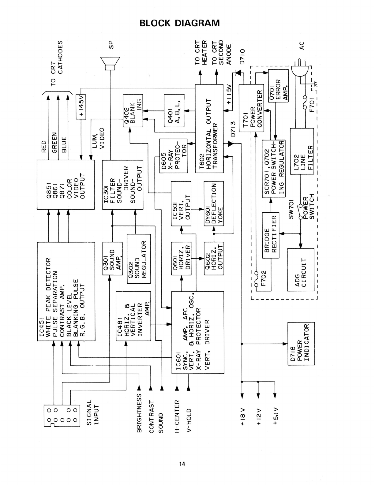
BLOCK
DIAGRAM
.....
.......
.....
.....
........
.....
......
.......
...
..........................
.. .. ..... ..
...........
....
......
14
AL
IGNMENT INSTRUCTIONS
1. B +
Power
Circuit
Adjustment
. . . . . . . . .. . . . . . . . . . . . . . . . . . . . . . . . . . . . . . . . . . .. . . .. .. . .. .. .. .. .. .. .. .. .. .. .. . . .. .. . . . .
16
2. Horizontal Hold
Adjustment
. . . . . . . . . . . . .. .
..
. . . .. . . . .. . . . . . .. . . . . .. .
..
..
..
. . .. . . . . .
..
. .
..
. . .... . . . .
.. . ..
. . .... . . . . .
16
3. Vertical Size
Adjustment
....
....
.... .
..
........... ......... ........ .......
........
.....
.......
.....
.....
.....
.... ...
16
4. Focusing . . . .
..
. . . . . .. . . .. . . . . . . . . . . . . . . . . . . . . . . . . . . . . . . . . . . . . . . . . . .. . . . . . . .
..
..
..
. . . . . .. . . . . . . . .. . . . . . . . . .
.. . ..
. . . . . . .. . . . 1 6
5. High
Voltage
Check
....
........
.......
..
......
......
......
................
.....................
...
...................
17
6. V
ertical-Linearity
Adjustment
.. .....
..
..... . ...... .....
.......... ............
.....
.............
.........
.. .........
17
7. X-ray Protector
Circuit
Test
.... .. ... .. ........... ..... ... .. ... ....................
.......
.......
..........
.........
17
. Color
Purity
Adjustment
. . . . . . . . . . . . . . . . . . . . . . . . . . . . . . . . . . . . . . . . . . . . . . . . . . . . . . . . . . . . . . . . . . . . . . . . . . . . . . . . . . . . . . . . . . . . . 1 7
9.
Black and
White
Tracking
. . . . . . . . . . . . . . . . . . . . . . . . . .. . . . . . . . . .. . . . . . . . . . . . . . . . . . . . . . . . . . . . . . . . . . . . . . . . . . . . . . . . . . . . . . 1 8
0.
Static
(Center)
Convergence
. . . . . . . . . . . . . . . . . . . . . . . . . . . . . . . . . . . . . . . . . . . . . . . . . . . . .. . . . . . .. . . . . . . . . . .. . . . . . . . . . . . . . . . 1 9
. Dy
namic
Convergence
. . . . . . . . . . . . . . . . . . . . . . . . . . . . . . . . . . . . . . . . .. . . . . . . . . . . . . . . . . . . . .. . . . . . . . . . . . . . . . . . . . . . .
..
. . . . . . . .
20
OU
BLESHOOTING GUIDE
...........
.........
........
...........
..... .. ..........
.....
.......
....
..... ..
......
..... ....
21
I
RI G DIAGRAM
AND
PARTS
LOCATION
....
....
..... .. ..................
.....
.....
...
............
....
........
..
25
I
TED
CIRCUIT BOARDS (Top and
Bottom
Views)
ain
PCB
...... ... ..
.........
........
...............
..........
........
.... ........
....
..... .... ...
.....
...... .........
....
....
27
CRT
Socket
PCB . . . . . . . . . . . . . . . . . . . . . . . . . . . . . . . . . . . . . . . . . . . . . . . . . . . . . . . . . . . . . . . . . . . . . . . . . . . . . . . . . . . . . . . . . . . . . . . . . . . . . . . . . . .
28
L
ED
PCB
.............. ............. ..
..................
.... .. ..
..........
...... ...... ....
.....
....
.......
...... .... .. ..
.......
28
CA
BINET EXPLODED VIEW/PARTS LIST
1.
Cabinet
Exploded
View
. .. . . . ..... .. . . . . . . . .
....
..... ... . . ......... .. ... . .. .... .. .... ... ....
......
....
..
...
..
. . . . .. . .
31
2. Cab
inet
Parts
List
............ ... ..........
......
...................
....
..... ....... ........... ... ....
.........
.. .. .. ...
33
3. Electrical Parts
List
........
......
....... ...
.............
.... ....... .. ...... .
.............
....
......
................
....
35
SCHEMATIC DI
AGRAM
...... ... .. .. ........ .....
.......
............ ....... ..... ......
.......................
.........
....
. 4 7
AV
EFORMS .................
.....
..........
....
.......
.....
.....
....... .... .. ....... ... ..
.....
...
.....
.....
........
.....
..... 50
SE !CONDUCTOR
LEAD IDENTIFICATION .... ............. ..
.......
.... .. .
..........
...
....
....... ... ..
........... 50
2
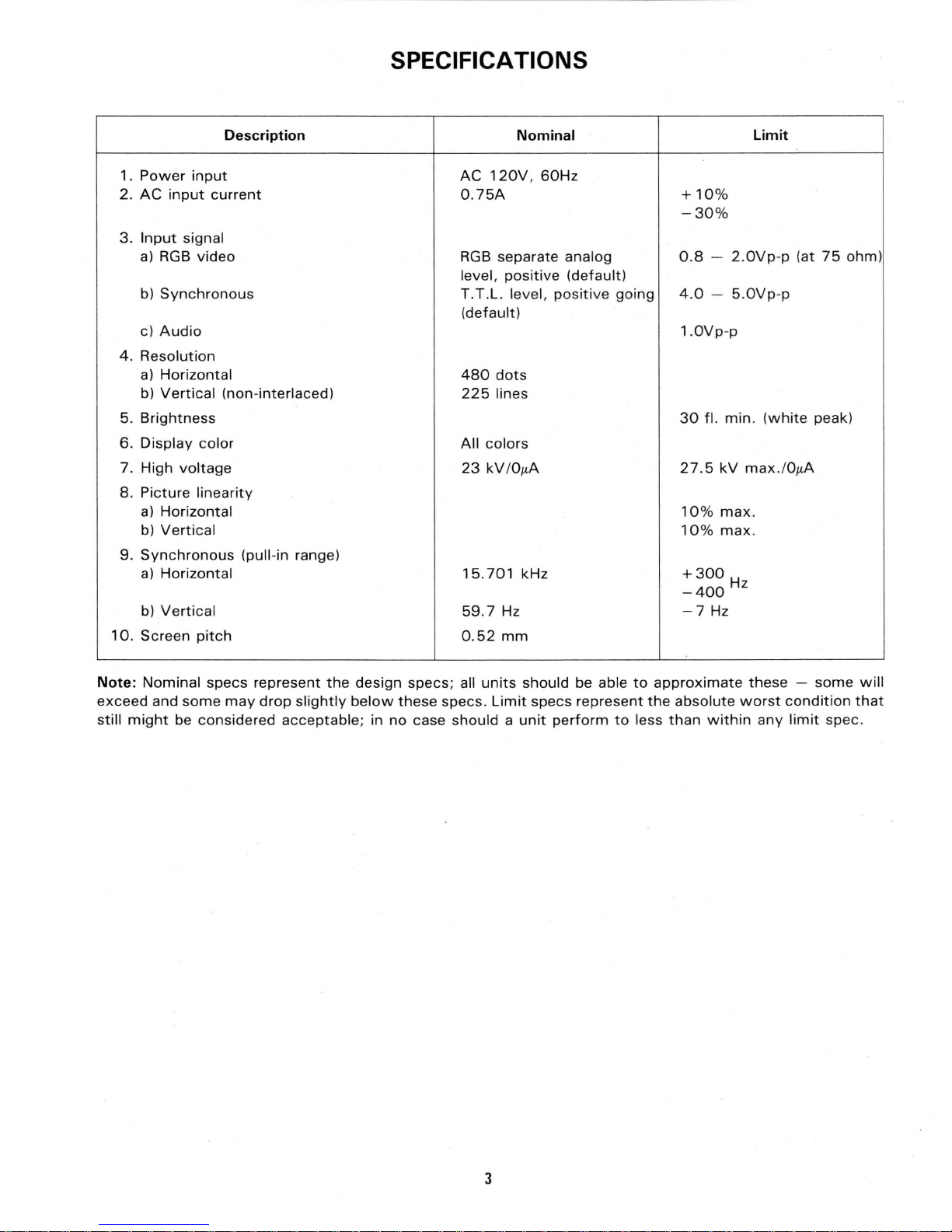
SPECIFICATIONS
1 .
Power
2.
AC
3.
Input signal
a)
RGB
b)
Synchronous
c)
Audio
4.
Resolution
a)
Horizontal
b)
Vertical
5.
Brightness
6.
Display
7.
High
8.
Picture
a)
Horizontal
b)
Vertical
9.
Synchronous
a)
Horizontal
Vertical
b)
10.
Screen
input
input
video
color
voltage
linearity
pitch
Description Nominal
AC 1 20V, 60Hz
current
0.75A
RGB
level,
separate
positive
T.T.L. level ,
(default)
480
dots
(non -
interlaced)
(pull-in range)
225
All
23
15.
59
. 7
0.52
lines
colors
kV /Oµ.A
701
kHz
Hz
mm
analog
(default)
positive
going
Limit
+
10%
-30%
0.8 -2.0Vp-p
4.0 -
1.0Vp
30
27.5
10%
10% max
+300
-400
-7
5.0Vp-p
-p
fl.
min. (white
kV
max./Oµ.A
max
.
.
H
z
Hz
(at
75
peak)
ohm)
Note:
exceed
still
might
Nominal
and
some
be
specs
considered
may
represent
drop
the
slightly
acceptable
design
below
; in
specs;
these
no
specs.
case
should a unit
all
units
Limit
should
specs
perform
be able
represent
to
to
approximate
the
absolute
less
than
these -some
worst
within
any
condition
limit
spec
will
that
.
3
IMPORTANT SERVICE SAFETY PRECAUTIONS
Service
work
should
be
performed
only
by
qualified
service
technicians
who
are
thoroughly
familiar
with
all
of
the
following
safety
checks
and
servicing
guidelines:
WARNING
1.
For
continued
safety,
do
not
attempt
to
modify
the
circuit.
2.
Disconnect
the
AC
power
before
servicing.
3.
Semiconductor
heat
sinks are
potential
shock
haz-
ards
when
the
chassis is
operating.
SERVICING
THE
HIGH
VOLTAGE SYSTEM
AND
PICTURE TUBE
When
servicing
the
high
voltage
system,
remove
the
static
charge by
connecting
a 10k
ohm
resistor in
series
with
an
insulated
wire
(such as a
test
probe)
between
the
chassis and
the
anode lead. (The AC line
cord
should
be
disconnected
from
the
AC
outlet.)
1.
The
picture
tube
in
this
display
monitor
employs
in-
tegral
implosion
protection.
2.
Replace
with a tube
of
the
same
type
number
for
continued
safety.
3.
Do
not
lift
the
picture
tube
by
the
neck
.
4. Handle
the
picture
tube
only
when
wearing shatter-
proof
goggles
and
after
discharging
the
high
volt-
age anode
completely.
X-RADIATION
AND
HIGH
VOLTAGE LIMITS
1.
Be
sure all
service
personnel are aware
of
the
procedures
and
instructions
covering X-radiation.
The
only
potential source
of
X-ray
in a current
solid-
state
display
monitor
is
the
picture
tube. However,
the
picture
tube
does
not
emit
measurable
X-ray
radiation
if
the
high
voltage
is as
specified
in
the
"
high-voltage
check"
instructions
.
It is
only
when
high
voltage
is
excessive
that
X-
radiation
is
capable
of
penetrating
the
shell
of
the
picture
tube,
including
the
lead
in
glass
material.
The
important
precaution
.is
to
keep
the
high
volt-
age
below
the
maximum
level
specified.
2.
It is essential
that
servicemen
have available
at
all
times
an
accurate
high
voltage
meter.
The
calibra-
tion
of
this
meter
should be
checked
periodically.
3.
High
voltage
should
always
be
kept
at
the
rated
value - no higher.
Operation
at
higher
voltages
may
cause a failure
of
the
picture
tube
or
high
volt
-
age
circuitry
and , also,
under
certain
conditions
,
may
produce
radiation in excess
of
desirable levels.
4
4.
When
the
high voltage regulator
is
operating proper-
ly
there
is
no
possibility
of
an
X-radiation
problem.
Every
time a color
chassis
is serviced,
the
bright-
ness should be
tested
while
monitoring
the
high
voltage
with a meter
to
be
certain
that
the
high
voltage
does
not
exceed
the
specified
value and
that
it
is
regulating
correctly
.
5.
Do
not
use a
picture
tube
other
than
that
specified
or
make
unrecommended
circuit
modifications
to
the
high
voltage
circuitry
.
6.
When
troubleshooting
and
taking
test
measure-
ments
on a
display
monitor
with
excessive
high
voltage, avoid being
unnecessarily
close
to
the
display
monitor. Do
not
operate
the
display
monitor
longer
than
is
necessary
to
locate
the
cause
of
excessive voltage.
BEFORE
RETURNING THE DISPLAY MONITOR
Fire and Shock Hazards
Before
returning
the
display
monitor
to
the
user, per-
form
the
following
safety
checks
:
1.
Inspect
all lead dress
to
make certain
that
the
leads
are
not
pinched
or
that
hardware
is
not
lodged
be-
tween
the
chassis
and
other
metal
parts
in
the
dis-
play
monitor.
2.
Inspect
all
protective
devices
such
as
nonmetallic
control
knobs,
insulating
materials,
cabinet
backs,
adjustment
and
compartment
covers or shield, iso -
lation
resistor-capacitor
networks,
mechanical
in-
sulators, etc.
3.
To
be sure
that
no
shock
hazard
exists, check
for
leakage
current
in
the
following
manner:
• Plug
the
AC
line cord
directly
into a 120-volt
AC
outlet.
(Do
not
use an isolation
transformer
for
this
test
.)
•
•
Using
two
clip leads,
connect
a 1.5k ohms,
10-watt
resistor
paralleled by a 0.15µF
capacitor
in series
with
all
exposed
metal
cabinet
parts
and a
known
earth
ground,
such
as an
electrical
conduit
or elec-
trical
ground
connected
to
earth
ground.
Use an
SSVM
or
VOM
with
1000
ohms-per-volt
or
higher
sensitivity
to
measure
the
AC
voltage
drop
across
the
resistor.
(See Figure 1 . )
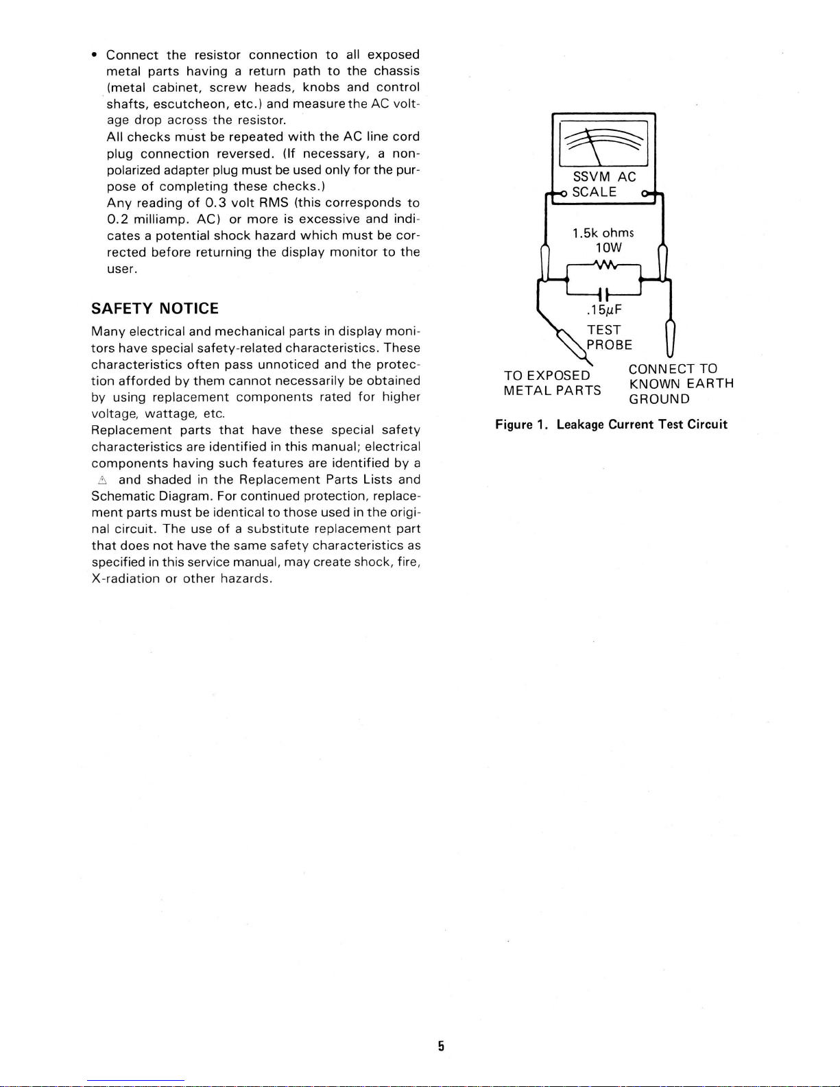
•
Connect
the
resistor
connection
to
all
exposed
metal
parts
having a return
path
to
the
chassis
(metal
cabinet,
screw
heads,
knobs
and
control
shafts,
escutcheon,
etc.)
and
measure
the
AC
volt
-
age
drop
across
the
resistor.
All
checks
must
be
repeated
with
the
AC
line
cord
plug
connection
reversed. (If
necessary, a non-
polarized adapter plug
must
be
used
only
for
the
pur-
pose
of
completing
these
checks.)
Any
reading
of
0. 3
volt
RMS (this
corresponds
to
0.2
milliamp.
AC)
or
more
is
excessive
and
indi-
cates a potential
shock
hazard
which
must
be
cor-
rected
before
returning
the
display
monitor
to
the
user.
SAFETY NOTICE
Many
electrical
and
mechanical
parts
in
display
moni-
tors
have special
safety-related
characteristics.
These
characteristics
often
pass
unnoticed
and
the
protec-
tion
afforded
by
them
cannot
necessarily
be
obtained
by
using
replacement
components
rated
for
higher
voltage,
wattage,
etc.
Replacement
parts
that
have
these
special
safety
characteristics
are
identified
in
this
manual;
electrical
components
having
such
features
are
identified
by
a
6 and shaded in
the
Replacement
Parts
Lists
and
Schematic
Diagram. For continued
protection,
replace-
ment
parts
must
be
identical
to
those
used in
the
origi-
nal
circuit.
The
use
of a substitute
replacement
part
that
does
not
have
the
same
safety
characteristics
as
specified in
this
service manual,
may
create
shock
, fire,
X-radiation
or
other
hazards.
5
SSVM
AC
SCALE
TO EXPOSED
METAL
PARTS
CONNECT
TO
KNOWN
EARTH
GROUND
Figure 1.
Leakage
Current Test Circuit
THEORY
OF
OPERATION
1.
RGB
Drive Circuit
IC451 is a linear
IC
to
amplify
the
RGB
signals.
The DC
restoration
system
of
IC451 provides
control
of
the
simultaneous
amplitude
(contrast)
and DC level
(brightness)
of
RGB
.
The
synchronizing
signal, as a DC restoration pulse, is
fed
from
pin @
of
IC601
to
pins @ and @
of
IC451.
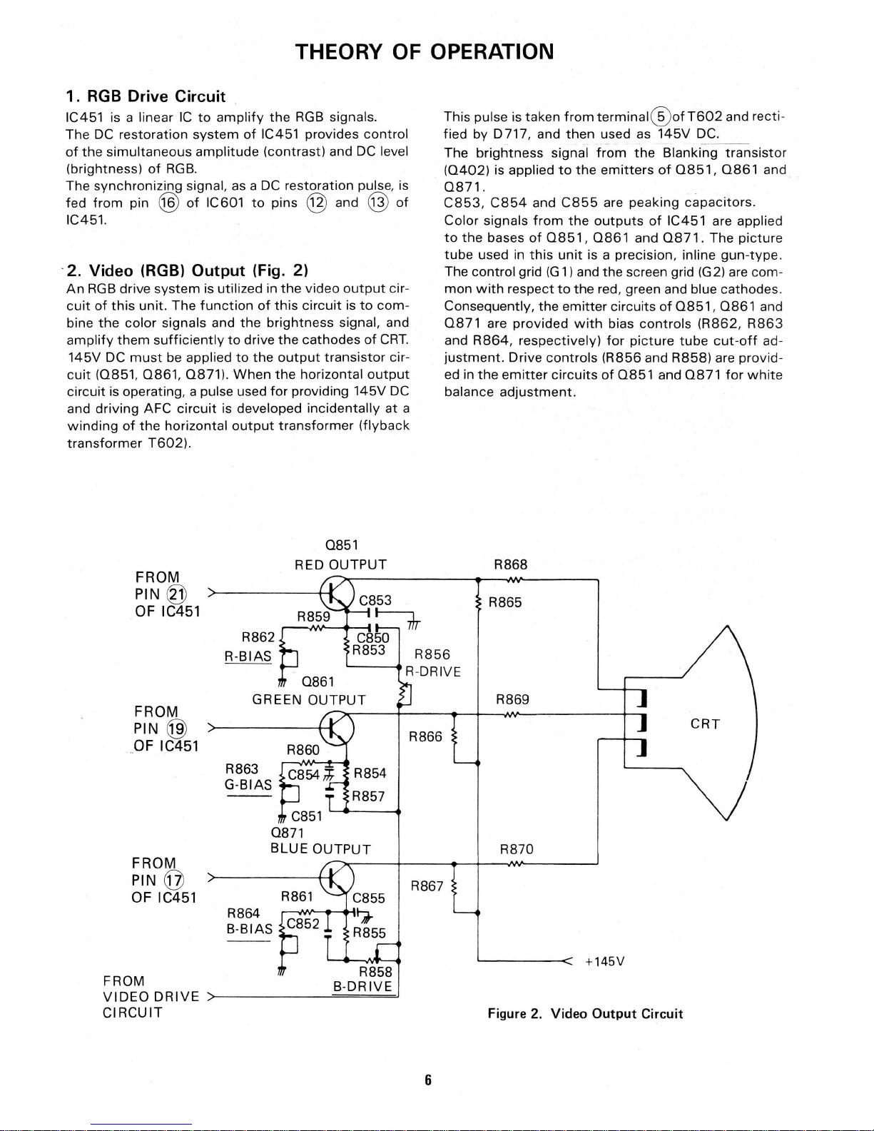
· 2. Video (RGB) Output (Fig. 2)
An
RGB
drive
system
is
util
ized in
the
video
output
cir-
cuit
of
this
unit. The
function
of
this
circuit
is
to
com-
bine
the
color
signals and
the
brightness
signal, and
amplify
them
sufficiently
to
drive
the
cathodes
of
CRT.
145V
DC
must
be applied
to
the
output
transistor
cir-
cuit
(0851,
0861,
0871).
When
the
horizontal
output
circuit
is operating, a pulse used
for
providing
145V
DC
and
driving
AFC
circuit
is developed
incidentally
at a
winding
of
the
horizontal
output
transformer
(flyback
transformer
T602).
0851
RED
OUTPUT
FROM
PIN@
OF
IC451
R862
R-BIAS
This pulse is taken
from
terminal@ofT602
and recti-
fied by
D717
, and
then
used as
145V
DC.
--··-
-
The
brightness
signal
from
the
Blanking
transistor
(0402)
is applied
to
the
emitters
of
0851,
0861
and
0871.
C853,
C854
and
C855
are
peaking
capacitors.
Color signals
from
the
outputs
of
IC451 are applied
to
the
bases
of
0851, 0861
and
0871
. The
picture
tube
used in
this
unit
is a precision, inline
gun-type.
The control grid
(G
1)
and the screen grid (G2) are com-
mon
with
respect
to
the
red, green and blue cathodes.
Consequently, the
emitter
circuits
of
0851,
0861
and
0871
are
provided
with
bias
controls
(R862, R863
and
R864,
respectively)
for
picture
tube
cut-off
ad-
justment.
Drive
controls
(R856
and
R858)
are provid-
ed in
the
emitter
circuits
of
0851
and
0871
for
white
balance
adjustment.
R868
R865
R856
0861
R-DRIVE
R869
FROM
PIN@)
CRT
R866
OF
IC451
R863
G-BIAS
C851
0871
BLUE
OUTPUT
R870
FROM
PIN@
R867
OF
IC451
R861
R864
C852
B-BIAS
---
+145V
FROM
R858
B-DRIVE
VIDEO
DRIVE
CIRCUIT
Figure 2.
Video
Output
Circuit
6
3.
Vertical Deflection Circuit
The
vertical
to
plied
Pin @
oscillator
controlled
be
varied
obtained
between
The
oscillator
through a buffer
0 , is
The
sawtooth
an
AC
The
output
(R
507)
The
verti
tegrating
sawtooth
4.
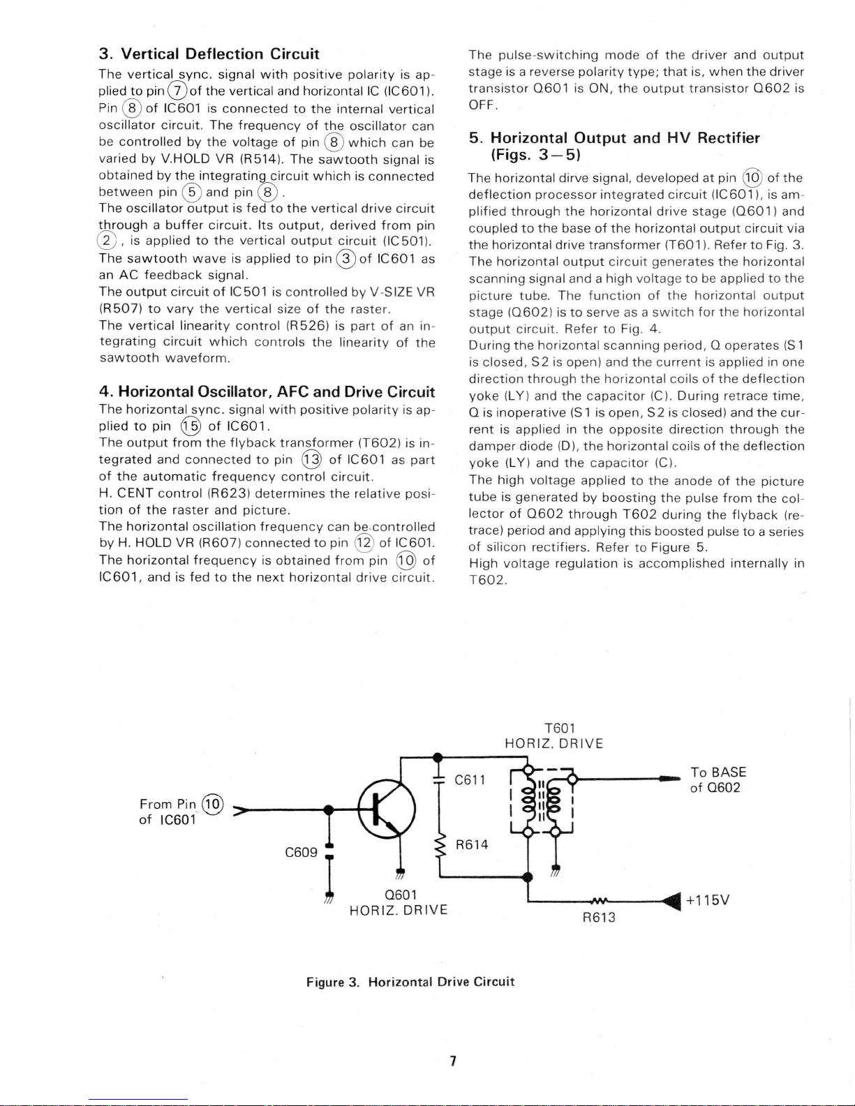
Horizontal Oscillator, AFC and Drive Circuit
The
horizontal
to
plied
The
output
tegrated
of
the
H.
CENT
tion
of
The
horizontal
by H. HOLD VR
The
horizontal
IC601, and
sync.
signal
pin
0of
the
vertical
of
IC601 is
circuit.
by
V.HOLD VR (R514).
by
the
pin @
applied
feedba
circuit
to
vary
ca l
linearity
circuit
waveform
pin @
from
and
automatic
control
the
raster
is
connected
The
by
the
voltage
integrating
and
pin @ . . . . .
output
ck
connected
fed
is
circuit.
to
the
wave
is
signal.
of
IC
the
vertical
control
which
.
sync.
signal
of
IC601
the
flyback
frequency
(R623)
and
oscillation
(R607)
frequency
to
the
with
and
frequency
of
The
circuit
fed
to
the
Its
output,
vertical
applied
501
is
controlled
size
(R
controls
with
.
transformer
to
pin @
control
determines
picture.
frequ
connected
is
obtained
next
horizontal
positive
horizontal
to
the
of
the
pin @
sawtooth
which
vertical
derived
output
to
pin@
of
the
526)
the
positive
of
circuit.
the
ency
can be.
to
pin @
polarity
IC
internal
oscillator
which
is
connected
drive
circuit
of
by
V-S IZE VR
raster
is
part
line
arity
polarity
(T602)
IC601
relative
from
pin @
drive
from
IC601
of
controlled
of
is ap-
(IC601
vertical
can
can
signal
c1rcu1t
(IC 501
.
an in -
of
is ap-
is in-
as
part
posi
IC601.
circuit.
be
is
pin
).
as
the
of
The
stage
transistor
).
OFF.
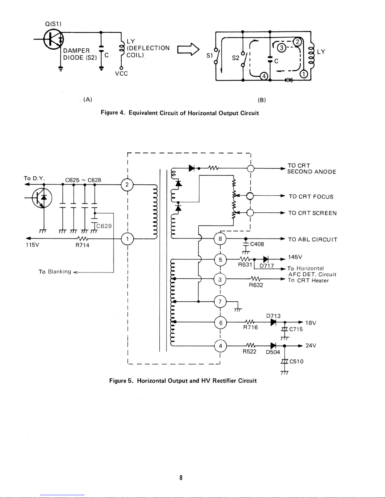
5. Horizontal Output and
The
deflection
plified
coupled
the
The
scanning
picture
stage
output
During
is
direction
yoke
O is
rent
damper
yoke
The
-
tube
lector
trace) period and
of
High
T602.
pulse-switching
is a reverse
0601
(Figs.
horizontal
horizontal
horizontal
closed,
inoperati
silicon
3-5)
processor
through
to
the
signal
tube. The
(0602)
circuit.
the
horizontal
S2
through
(LY)
and
ve
is
applied
diode
(LY) and
high
voltage
is
generated
of
0602
rectifiers. Refer
voltage
drive
is
regulation
mode
polarity
is ON,
dirve signal,
the
base
output
and a
is
to
Refer
open)
the
(S
in
(D),
the
through
applying
the
integrated
horizontal
of
the
transformer
circuit
high
function
serve as a
to
scanning
and
the
horizontal
capacitor
1 is
open,
the
opposite
the
horizontal
capacitor
applied
by
boosting
of
the
type;
that
output
transistor
HV
developed
circuit
drive
horizontal
(T601
generates
voltage
Fig. 4.
the
to
T602 during
this
to
is
accomplished
to
of
the
switch
period, 0 operates
current
coils
(C).
During
S2
is
closed)
direction
coils
(C).
the
anode
the
pulse
boosted
Figure
driver
is,
and
when
Rectifier
at
pin @
(IC601
stage
(0601)
output
).
Refer
the
be
applied
horizontal
for
the
is
applied
of
the
retrace
and
through
of
the
of
the
from
the
flyback
pulse
5.
internally
output
the
driver
0602
of
the
),
is
am-
and
circuit
horizontal
horizontal
deflection
deflection
to
to
Fig. 3.
to
output
in one
time
the
picture
the
a series
via
the
(S
cur
the
co l-
(re
is
1
,
-
-
in
From
Pin.@
of
IC601
C609 l
HORIZ. DRIVE
C611
R614
0601
HOR IZ. DR
IVE
Figure 3. Horizontal Drive Circuit
7
T60
1
R613
To
of
BASE
0602
O(S1)
To
D.Y.
DAMPER I
DIODE
':'
C625 - C628
(S2)
(A)
.,.
C
LY
(DEFLECTION
COIL)
vcc
c::)
s1J
I
r
r
52
1:
L@I--
"'----------"4---·1·---
Figure 4. Equivalent Circuit of Horizontal Output Circuit
r---
1
(B)
i------TO
)-------
1-----
r@=--
2
c - :
_ _)1
CRT
SE.COND
TO
CRT
TO
CRT
LY
ANODE
FOCUS
SCREEN
115V
To
Blanking
R714
~
---
~
I_
---
Figure 5. Horizontal Output
---
--
and
1----'Vlt1----
l----JV.,..,_---1t-.....-__,~18V
HV
Rectifier Circuit
'------To
AFC
To
C715
C510
H
orizontal
DET
CRT
Heater
. Circuit
8
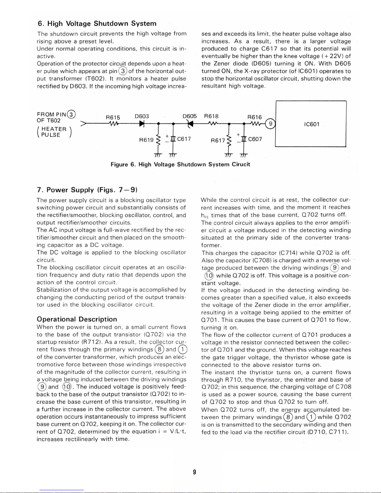
6.
High
Voltage
Shutdown
System
The
shutdown
circuit
prevents
the
high
voltage
from
rising
above a preset
level.
Under
normal
operating
conditions,
this
circuit
is inactive.
Operation
of
the
protector
circuit
depends
upon a heat
-
er
pulse
which
appears
at
pin@
of
the
horizontal
out
-
put
transformer
(T602). It
monitors a heater
pulse
rectified
by
0603. If
the
incoming
high
voltage
increa-
R615
0603 0605
ses
and
exceeds
its
limit, the
heater
pulse
voltage
also
increases.
As a result,
there
is a
larger
voltage
produced
to
charge
C617
so
that
its
potential
will
eventually
be
higher
than
the
knee
voltage
( +
22V)
of
the
Zener
diode
(0605)
turning
it
ON.
With
D605
turned
ON,
the
X-r
ay
protector
(of
IC601)
operates
to
stop
the
horizontal
oscillator
circuit,
shutting
down
the
resultant
high
voltage.
R618
FROM
PIN@
OF
T602
~~-91~--41>----41>-----4--~-l\.IV'-~---~----'VVI
IC601
(
HEATER
)
PULSE
R619
+
+
C617
C607
Figure
6.
High
Voltage
Shutdown
System
Cirucit
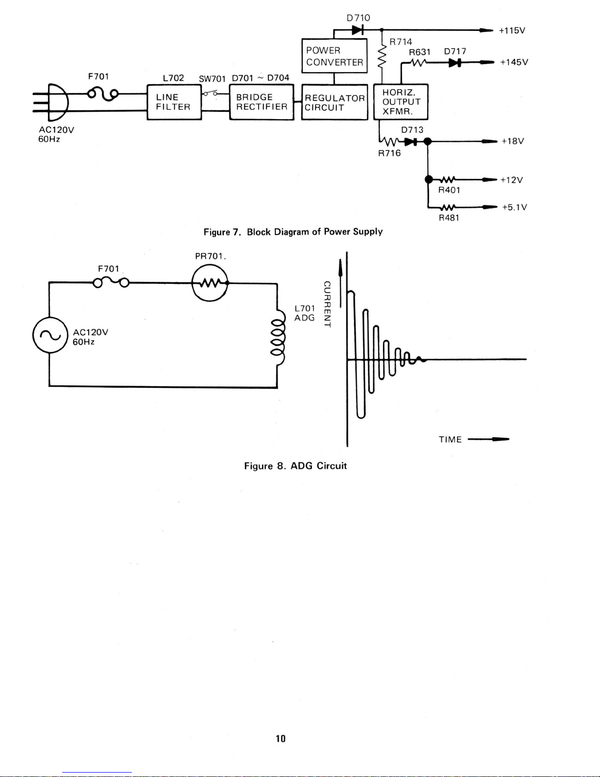
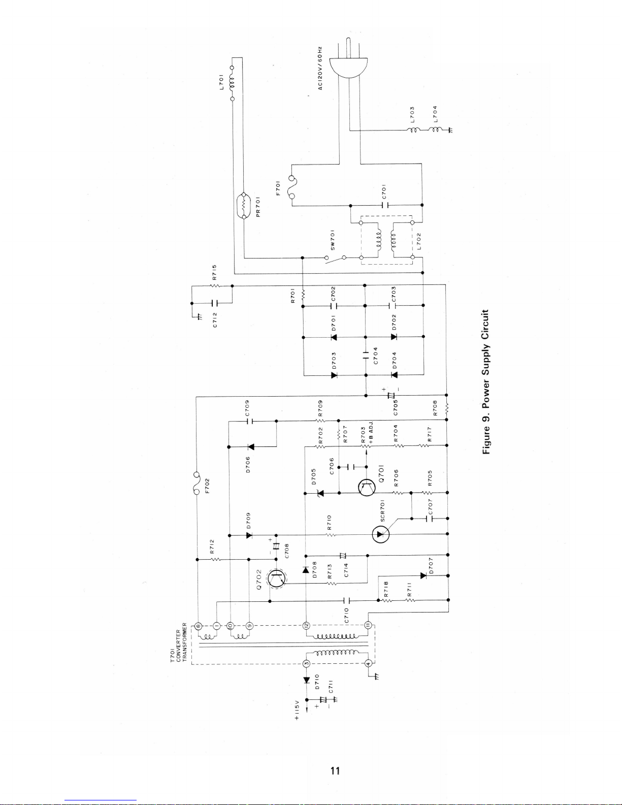
7.
Power
Supply
(Figs.
7-9)
The
power
supply
circuit
is a
blocking
oscillator
type
switching
power
circuit
and
substantially
consists
of
the
rectifier/smoother, blocking
oscillator,
control,
and
output
rectifier/smooth
er
circuits.
The
AC
input
voltage
is
full-wave rectified
by
the
rec
-
tifier/smoother
circuit
and
then
placed
on
the
smooth-
ing
capacitor
as a DC
voltage.
The
DC
voltage
is
appli
ed
to
the
blocking
oscillator
circuit
.
The
blocking
oscillator
circuit
operates
at
an
oscilla
-
ti
on
frequency
and
duty
ratio
that
depends
upon
the
action
of
the
control
circuit.
St
abilization
of
the output
voltage
is
accomplished
by
changing
the
conducting
period
of
the output transis-
tor
used
in
the
blocking
oscillator circuit.
Operational
Description
When
the
power
is
turned on, a
small
current
flows
to
the
base
of
the
output
transistor
(0
702
) via t he
startup
resistor (R712
).
As a result, the
collector cur-
rent
flows
through
the pri
mary
windings@
and
Q)
of
the
converter
transformer, whi
ch
produ
ce s an elec -
tromotive
force
between
those
windings irrespective
of
the
magnitude
of
the
collector
current,
resulting
in
a
voltage
being
indu
ced
between
the
driving windings
@
and
@.
The
induced
voltage
is
positively
feed-
back
to
the
base
of
the
output
transistor
(0
702) to
in-
crease
the
base
current
of
this
transistor, resulting
in
a
further
increase
in
the
collector
current.
The
above
operation
occurs
instantaneously
to
impress
sufficient
base
current
on 0 702, keeping
it
on.
The
collector
cur
-
rent
of 0 702, determined
by
the
equation
i = V /L ·t,
increases
rectilinearly
with
time.
9
While
the
control
circuit
is
at
rest, the
collector
cur
-
rent
increases
with
time, and
the
moment
it
reaches
h
FE
times
that
of
the
base
current, 0 702
turns
off.
.
The
control
circuit
always
applies
to
the
error
amplifi
-
er
circuit a voltage
induced
in
the
detecting
winding
situated
at
the
primary
side
of
the
converter
trans
-
former
.
This
charges
the
capacitor
(C714)
while
0702
is
off
.
Also
the
capacitor (C708)
is
cha
rged
with
a reverse vol-
ta
ge
produced
between
the
driving
windings
@
and
@
while 0 702
is
off. This
voltage
is a
positive
con-
stant
voltage
.
If
the
voltage
induced
in
the
detecting
winding
be -
comes
greater
than a specified
value,
it
also
exceeds
the
voltage
of the
Zener
diode
in
the
error
amplifier,
resulting
in a
voltage
being
applied
to
the
emitter
of
0701. This
causes
the
base
current
of
0701
to
flow
,
turning
it on.
The
flow
of
the
collector
current of
0701
produces
a
voltage
in
the
resistor
connected
between
the
collec
-
tor
of
0701
and
the
ground. When
this
voltage
reaches
the
gate
trigger
voltage, the
thyristor
whose
gate
is
connected
to
the
above
resistor
turns on.
The instant
the
thyristor
turns on, a
current
flows
through
R710, the
thyristor, the
emitter
and
base
of
0
702
; in
this
sequence, the
charging
voltage
of C 708
is
used
as a
power
source, causing
the
base
current
.
of 0 702
to
stop
and
thus 0 702
to
turn
off.
When Q 702
turns
off,
the
energy
accumulated
be-
tween
the
primary
windings@
and
G)
while
0702
is
on
is
transmitted
to
the
secondary
winding
and
then
fed
to
the
load
via
the
rectifier
circuit
(D
71
0, C 711).
AC120V
60Hz
F701
F701
L702
LINE
FILTER
SW701
Figure 7.
PR701 .
POWER
CONVERTER
0701
,...:,
0704
BRIDGE
RECTIFIER
Block Diagram of Power Supply
REGULATOR
CIRCUIT
0710
R714
HORIZ.
OUTPUT
XFMR
R716
R631
.
0717
R401
R481
+115V
+145V
+18
V
+12V
+5.1V
AC120V
60Hz
Figure 8 .
L701
ADG
ADG
~
f
m
z
--i
Circuit
TIME
---
10
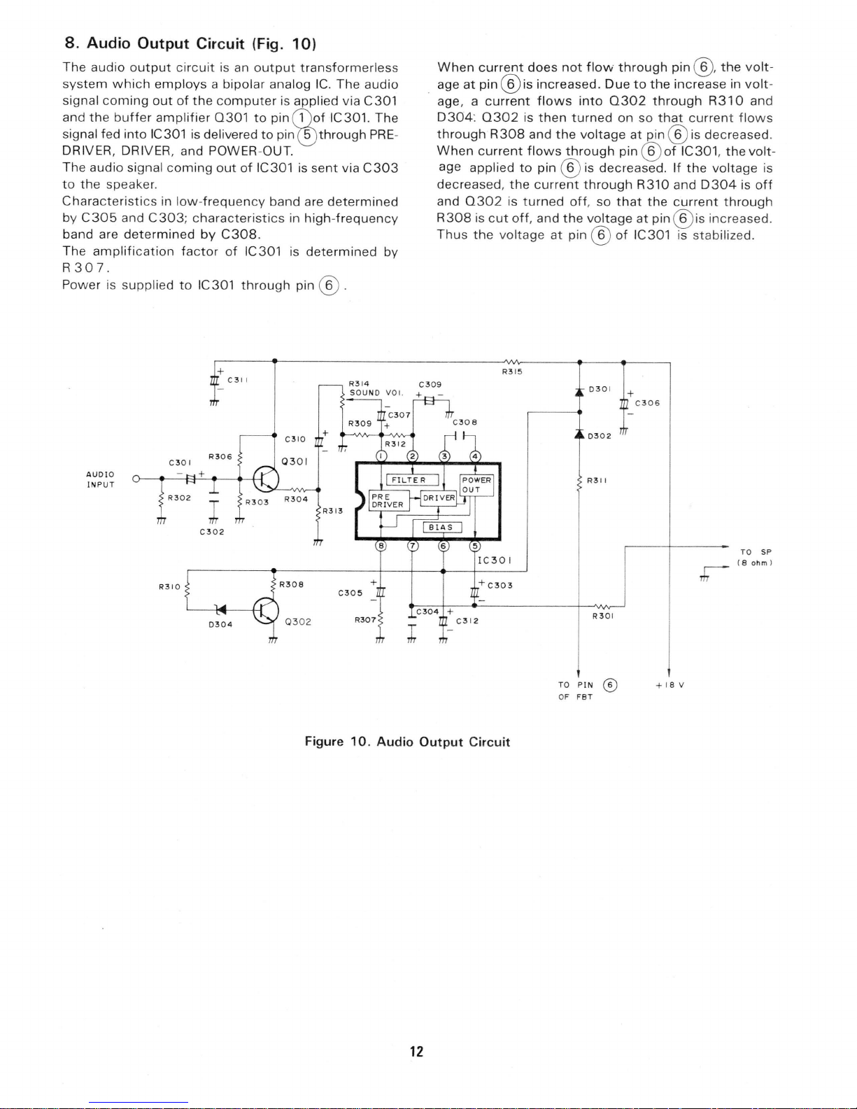
8.
Audio Output Circuit (Fig.
The audio
system
signal
and
signal fed into
DR
IVER, DRIVER, and POWER-OUT.
The audio signal
to
the
Characteristi
by
C305
band are
The
30
R
Power
output
which
coming
the
buffer
employs
out
amplifier
IC301
speaker.
cs in
and
C303; characteristi
determined
amplification
7.
is
supplied
circuit
of
the
is
delivered
coming
low
-frequ e
by
factor
to
IC301
is an
a bipolar analog
computer
0301
out
of
ncy
C308
of
IC301 is
through
+
C3 1 I
10)
output
to
IC301 is
transformerless
is
applied via C301
pin(Dof
to
pin ®
band are
cs in
high-frequency
.
determined
pin
IC.
The
IC301. The
through
sent
via
determined
@.
R3
SOUN D
audio
PRE
C303
by
14
VOi.
-
C3
When
current
age
at
pin@
age, a
current
D304: 0302
through
When
R308
current
age applied
decreased,
and
0302
R308
is
cut
Thus
the
09
does
is increased.
flows
is
then
and
flows
to
pin @
the cur
is
turned
off
, and
volt
age
R3
15
not
turned
the
through
rent
off
the
at
pin @
flow
Due
into
0302
voltage
is
decreased
through
, so
voltage
0 3 0 1
03
0 2
through
on so
pin @
that
of
+
pin
@,
to
the
increase in
through
that
at
pin@ is decreased .
of
. If
R310 and
the
at
pin @ is increase d.
R310
current
IC301 ,
the
D304
current
IC301 is stabilized.
C3 0 6
the
volt
volt
and
flows
the
volt
voltage
is
through
-
-
-
is
off
R310
03
02
Figure 10. Audio Output Circuit
TO
OF
PIN
FBT
R3
1 I
TO SP
( 8 ohm )
R3
01
®
+1
a v
12
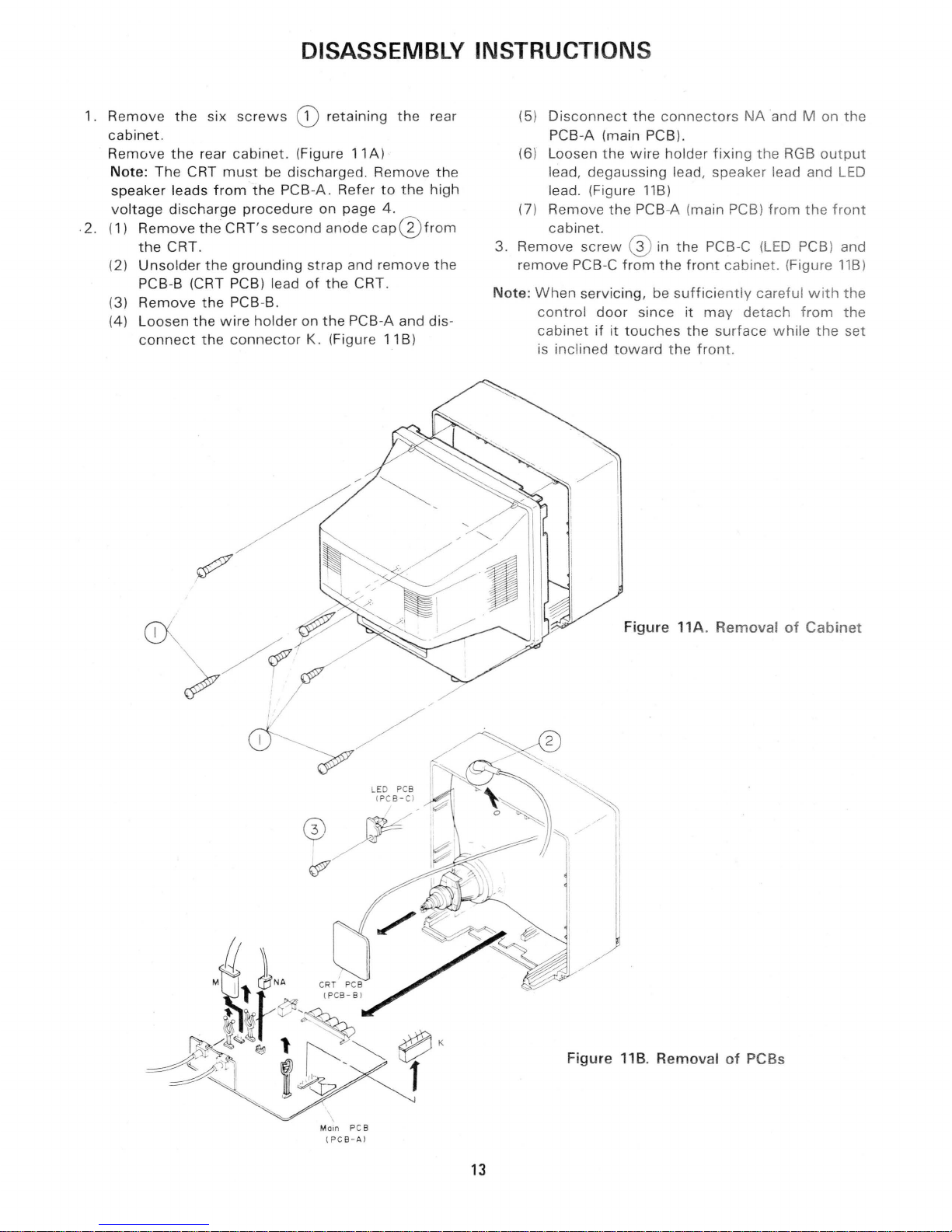
DISASSEMBLY INSTRUCTIONS
1.
Remove
the
six
screws
Q)
retaining
the
rear
cabinet.
Remo ve
the rear
cabinet.
(Figure
11A)
Note: The CRT
must
be
discharged
. Remove
the
speaker
leads
from
the
PCB-A. Refer
to
the
high
voltage
discharge
procedure
on page 4.
.2. (1)
Remove the
CRT's
second anode cap @
from
the
CRT .
(2)
Unso
lder
the
grounding
strap
and
remove
the
PCB
-B
(CRT PCB) lead
of
the
CRT.
(3)
Remove
the
PCB-B.
(4) Loosen
the
wire
holder
on
the
PCB-A and dis-
connect
the
connector
K. (Figure 11B)
'
\
Ma
in
PC 8
( P CB- A l
13
(5)
Disconnect
the
conn
ect
ors
NA
and M on
the
PCB-A (main PCB).
(6) Loosen
the
wire
hold er fi
xing
the
RGB
output
lead,
degaussing
lead, speaker lead and
LED
lead. (Figure 118)
(7) Remove
the
PCB-A (
main
PCB)
from
the
fron
t
cabinet
.
3. Remove
screw
@ in
the
PCB
-C
(LED PC
B)
and
remove
PCB-C
from
the
front
cabinet. (Figure 118)
Note:
When
servicing, be
suff
ici
ently
careful
with
the
control
door
since
it may
detach
from
the
cabinet
if
it
touches
the surface while
the
set
is inclined
toward
the front.
Figu
re
11A. Removal
of
Cabinet
Figure
11B.
Removal of PCBs
 Loading...