

•
TANDY COMPUTER PRODUCTS
TANDY 1000
HX
TECHNICAL REFERENCE MANUAL
Cat. No. 25-1513
.
TANDY COMPUTER PRODUCTS -
Tandy 1000
HX
Technical Reference Manual
Copyright 1987, Tandy Corporation.
All Rights Reserved.
Reproduction
or
use
of any
portion
of
this manual without
express written permission from Tandy Corporation and/or
its
licensor,
is
prohibited. While reasonable efforts have been
taken
in
the preparation
of
this manual
to
assure
its
accuracy, Tandy Corporation assumes
no
liability resulting
from any errors
in or
omissions from this manual,
or
from
the use
of the
information obtained herein.
•
TANDY COMPUTER PRODUCTS -
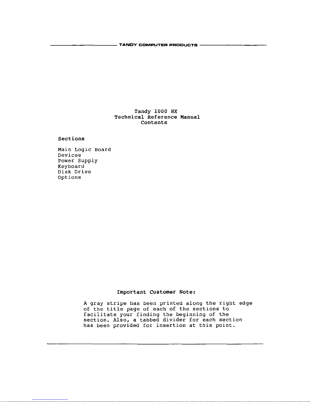
Tandy 1000 HX
Technical Reference Manual
Contents
Sections
Main Logic Board
Devices
Power Supply
Keyboard
Disk Drive
Options
Important Customer Note:
A gray stripe has been printed along the right edge
of the title page of each of the sections to
facilitate your finding the beginning of the
section. Also, a tabbed divider for each section
has been provided for insertion at this point.
•
TANDY COMPUTER PRODUCTS
1000
HX
Main Logic Board
•
TANDY COMPUTER PRODUCTS
1000 HX Main Logic Board
Contents
Section Page
Introduction
1
Specifications
3
Connector Pin Assignments
4
Option Card Description
8
Bus Interface Specifications
13
Signal Listing
13
System Timing
17
Theory of Operation
21
Main Logic Board
21
CPU Function
21
Non-CPU Function, Main Logic Board
21
Processor Address/Data Interface
21
CPU Control Signal Generation
24
IFL Equations
25
System Control Signal Generation
25
Bus Specification
25
Interrupt Function
28
Bus Interface
30
Keyboard/Timer/Sound Timer Circuits
30
Keyboard Interface
30
Timer Function
32
Sound Function
32
Joystick Interface
35
Printer Interface
35
Floppy Disk Controller Interface
38
Video System Logic
39
Main System Board RAM Timing
42
I/O Map Summary
45
Video/System Memory Address Map
62
Schematic Diagrams
63
.
TANDY COMPUTER PRODUCTS
INTRODUCTION
TO
THE TANDY 1000
HX
COMPUTER
The Tandy 1000
HX
Computer
is
modular
in
design
to
allow
maximum flexibility
in
system configuration. The computer
consists
of a
Main Unit, and a monitor. The Main Unit
is
supplied with one 3 1/2" internal disk drive.
A
second
internal 3 1/2" disk drive
is
optional. Each disk drive
has
a capacity
of
720K bytes formatted. The standard types
of
monitors used with the Tandy 1000
HX
are the monochrome
composite and the color RGB monitor.
The Tandy 1000
HX
has a standard 256K
of
system RAM.
An
optional DMA/RAM board allows the Tandy 1000
HX to be
expanded
by
128K
or
384K
of
RAM. This board will fit onto
the expansion slot. With a fully populated RAM board
installed, the Tandy 1000
HX
will have 640K bytes
of
RAM
allowed
by
the system memory map.
Other features include a parallel printer port, two built-in
joystick interfaces, and a headphone connection for private
listening.
The Main Unit
is
the heart
of
the Tandy 1000 HX.
It
houses
the Main Logic Assembly, system power supply,
internal 3 1/2" disk drive, and keyboard.
The Main Logic Assembly
is a
large board mounted
to
the
bottom of the Main Unit and interconnected
to
the keyboard,
power supply, and disk drive
by a
series
of
cables. Figure
1
shows the Tandy 1000
HX.
The Power Supply
is a
28W switching regulator type, designed
to provide adequate power capacity for a fully configured
system.
The Internal 3 1/2" Disk Drive uses double-sided,
double-density diskettes
to
read, write,
or
store data.
These are soft sector diskettes. The Disk Drive assembly
is
installed
in
the standard unit. All system programs, with
the exception
of
the system startup sequence, are stored
on
disk.

•
TANDY COMPUTER PRODUCTS
Either a monochrome
or a
color display may
be
used with
the
Tandy 1000 HX. The monochrome monitor
is a
high-resolution
green phosphor display which provides excellent visual
quality.
It
features a 12" screen with
an
anti-glare
surface.
Each display
is
capable
of 25
lines
of 80
characters.
The character matrix
is 8
wide
x 9
high.
Figure 1. TANDY 1000
HX
TANDY COMPUTER PRODUCTS
SPECIFICATIONS
Processor: Intel 8088-2
Dimensions:
3
1/4
x 17 x 14 1/2
(HWD)
Weight:
11
lbs
Power Requirements: 120 VAC,
60 Hz
With 3 1/2" Disk Drives, Memory Cards, and RS-232:
AC Current:
0.7 -
0.8 Amps with Floppy doing R/W tests.
Leakage Current: 0.5
mA
Power Supply Output:
+5 VDC 3.0 Amps max.,
1.9
Amps Typ.
+12 VDC 2.0 Amps max. 1.2 Amps continuous
-12 VDC .1 Amp max.
Environment:
Air Temperature
System ON:
55 to 85
degrees F (13
to
30 degrees
C)
System OFF: -40
to
150 degrees
F (-40 to 69
degrees
C)
Humidity: System ON-OFF:
8% to
80%
Disk Drive Specifications
Power:
Supply
Voltage
+5
VDC Input
Ripple
0 to 50 kHz 0.1 Vpp
Tolerance
Including Ripple
+/-5%
Standby Current
Nominal 50
mA
Average Current
(Read)
Peak Current
(Motor Start)
Peak Current
(Stepping during Motor
On)
Operating Current
Nominal 240
mA
+12
0.1
0.3
130
500
450
VDC Input
Vpp
mA
mA
mA
mA

•
TANDY COMPUTER PRODUCTS
Connector Pin Assignments
Jl
—
J2
—
J3
—
Speaker Interface
(2-Pin Vertical Header)
1 — Sound
PWRf NUMf CAP
1 — Power Indicator
3 — Num Indicator
5 — CAPS Indicator
Keyboard Interface
J4
—
1
—
2
—
3
—
4
—
5
—
6
—
Fan
1
—
XI
X5
X4
X3
X2
X6
+12V
2 — Ground
2 — Gnd
4 — NUMLOCK Control
6 — CAPS Control
7
— XO
8
— X7
9
— X3
10
— XI
11
— X5
12
— X4
2 — GND
J5
— DC
POWER
(6-Pin Vertical Header)
1 — +5 VDC
3 — GND
5 — +12V
J6 — Keyboard Interface
1
— Y0
2
— Yl
3 — Yll
4
— Y2
5
— Y3
6
— Y4
7
— Y5
J7 — Audio Jack
1 — GND
2
4
6
8
9
10
11
12
13
— +5 VDC
— Ground
12V
—
Y6
—
Y7
—
Y8
—
Y9
— Y10
— Yll
2 — AUDIOOUT
•
TANDY COMPUTER PRODUCTS
J8 — Right Joystick
(6-Pin Rt. Angle Circular Din)
1
— Y
Axis
2 — X
Axis
3 — Ground
4 —
Switch
1
5
— +5
VDC
6 —
Switch
2
J9 — Left Joystick
(6-Pin Rt. Angle Circular Din)
1
— Y
Axis
2 — X
Axis
3 — Ground
4 —
Switch
1
5
— +5
VDC
6 —
Switch
2
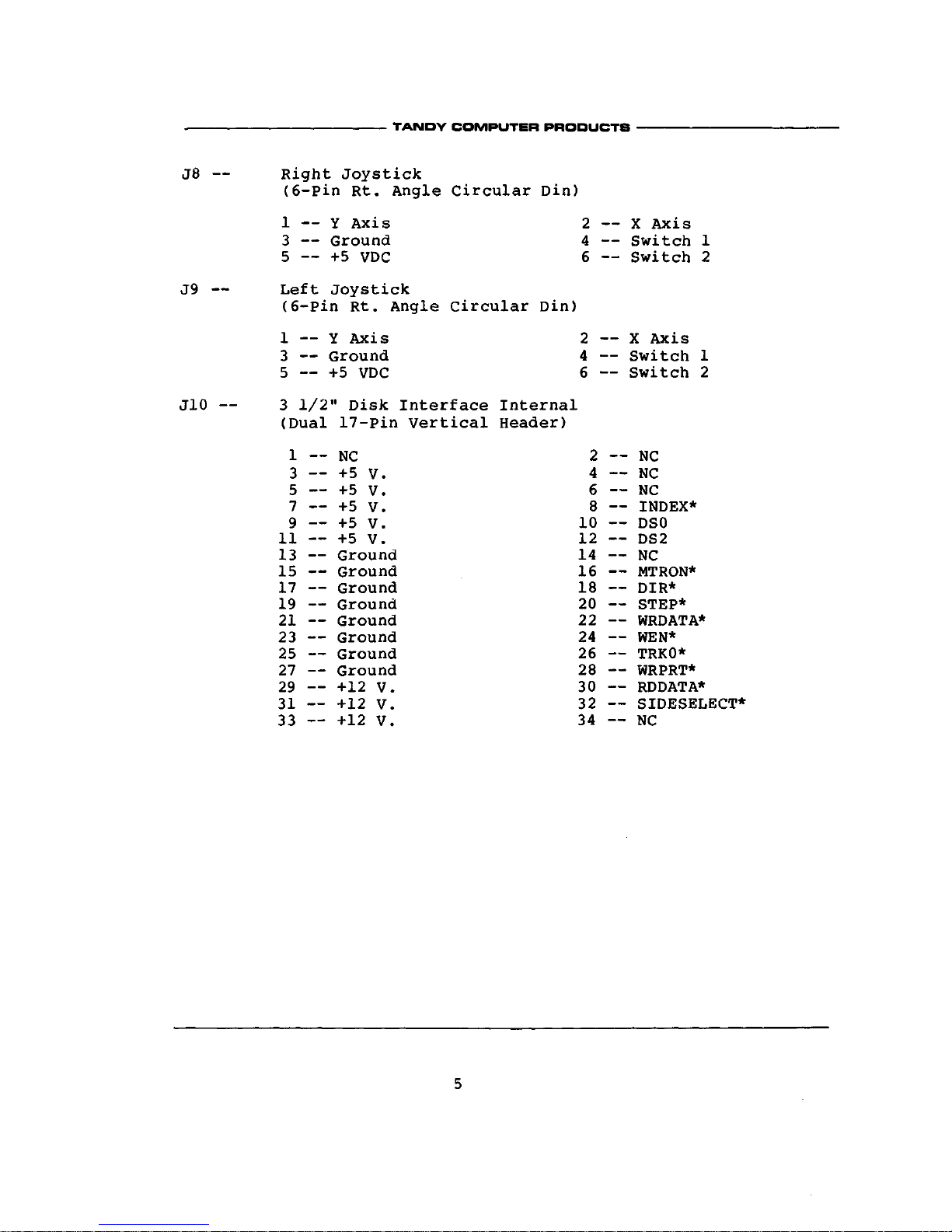
J10
— 3
1/2" Disk Interface Internal
(Dual 17-Pin Vertical Header)
1
3
5
7
9
11
13
15
17
19
21
23
25
27
29
31
33
—
NC
— +5
V.
— +5
V.
— +5
V.
— +5
V.
— +5
V.
— Ground
— Ground
— Ground
— Ground
— Ground
— Ground
— Ground
— Ground
— +12
V.
— +12
V.
— +12
V.
2
4
6
8
10
12
14
16
18
20
22
24
26
28
30
32
34
—
NC
—
NC
—
NC
— INDEX*
— DSO
— DS2
—
NC
— MTRON*
— DIR*
— STEP*
— WRDATA*
— WEN*
— TRKO*
— WRPRT*
— RDDATA*
— SIDESELECT*
—
NC
.
TANDY COMPUTER PRODUCTS
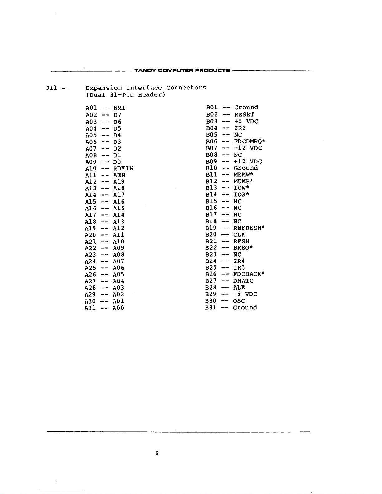
Jll
—
Expansion Interface Connectors
(Dual 31-Pin Header)
A01
A02
A03
A04
A05
A06
A07
A08
A09
A10
All
A12
A13
A14
A15
A16
A17
A18
A19
A20
A21
A22
A23
A24
A25
A26
A27
A28
A29
A30
A31
—
NMI
—
D7
—
D6
—
D5
—
D4
—
D3
--
D2
—
Dl
—
DO
—
RDYIN
—
AEN
—
A19
—
A18
—
A17
—
A16
—
A15
—
A14
—
A13
—
A12
—
All
—
A10
—
A09
—
A08
—
A07
—
A06
—
A05
—
A04
—
A03
—
A02
—
A01
—
A00
B01
B02
B03
B04
B05
B06
B07
B08
B09
BIO
Bll
B12
B13
B14
B15
B16
B17
B18
B19
B20
B21
B22
B23
B24
B25
B26
B27
B28
B29
B30
B31
—
Ground
—
RESET
—
+5
VDC
—
IR2
—
NC
—
FDCDMRQ*
12
VDC
—
NC
—
+12
VDC
—
Ground
—
MEMW*
—
MEMR*
—
IOW*
—
IOR*
—
NC
—
NC
—
NC
—
NC
—
REFRESH*
—
CLK
—
RFSH
—
BREQ*
—
NC
—
IR4
—
IR3
—
FDCDACK*
—
DMATC
—
ALE
—
+5 VDC
—
OSC
—
Ground
TANDY COMPUTER PRODUCTS
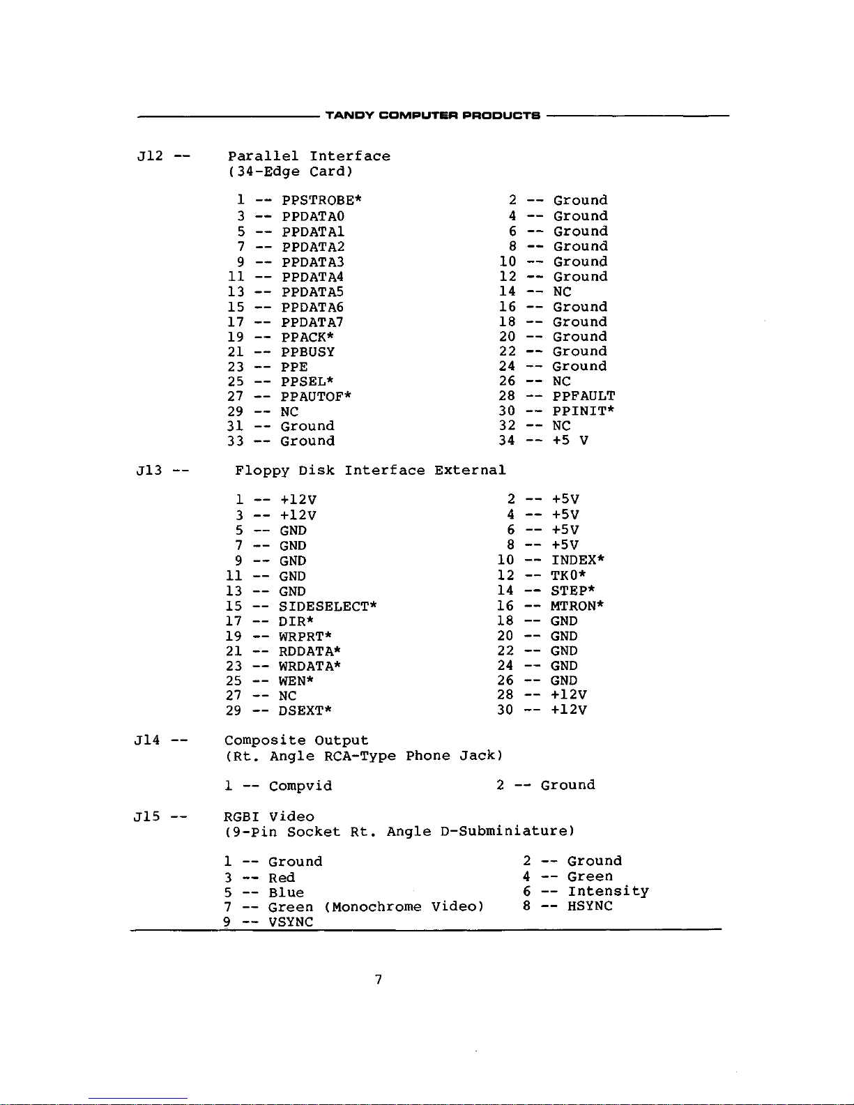
J12
--
J13
—
J14
—
J15
—
Parallel Interface
(34-Edge Card)
1 — PPSTROBE*
3 — PPDATAO
5 — PPDATAl
7 — PPDATA2
9 — PPDATA3
11 — PPDATA4
13 — PPDATA5
15 — PPDATA6
17 — PPDATA7
19 — PPACK*
21 — PPBUSY
23 — PPE
25 — PPSEL*
27 — PPAUTOF*
29
— NC
31 — Ground
33 — Ground
2 — Ground
4 — Ground
6 — Ground
8 — Ground
10 — Ground
12 — Ground
14
— NC
16 — Ground
18 — Ground
20 — Ground
22 — Ground
24 — Ground
26
— NC
28 — PPFAULT
30 — PPINIT*
32
— NC
34 — +5
V
Floppy Disk Interface External
1 — +12V
3 — +12V
5 — GND
7 — GND
9 — GND
11 — GND
13 — GND
15 — SIDESELECT*
17 — DIR*
19 — WRPRT*
21 — RDDATA*
23 — WRDATA*
25 — WEN*
27
— NC
29 — DSEXT*
Composite Output
2 -- +5V
4 — +5V
6 — +5V
8 — +5V
10 — INDEX*
12 — TKO*
14 — STEP*
16 — MTRON*
18 — GND
20 — GND
22 — GND
24 — GND
26 — GND
28 ~ +12V
30 -- +12V
(Rt.
Angle RCA-Type Phone Jack)
1 — Compvid
RGBI Video
2 — Ground
(9-Pin Socket Rt. Angle D-Subminiature)
1 — Ground
3 — Red
5 — Blue
7 — Green (Monochrome
9 ~ VSYNC
2 — Ground
4 — Green
6 — Intensity
Video)
8 —
HSYNC
- TANDY COMPUTER PRODUCTS -
•
TANDY COMPUTER PRODUCTS
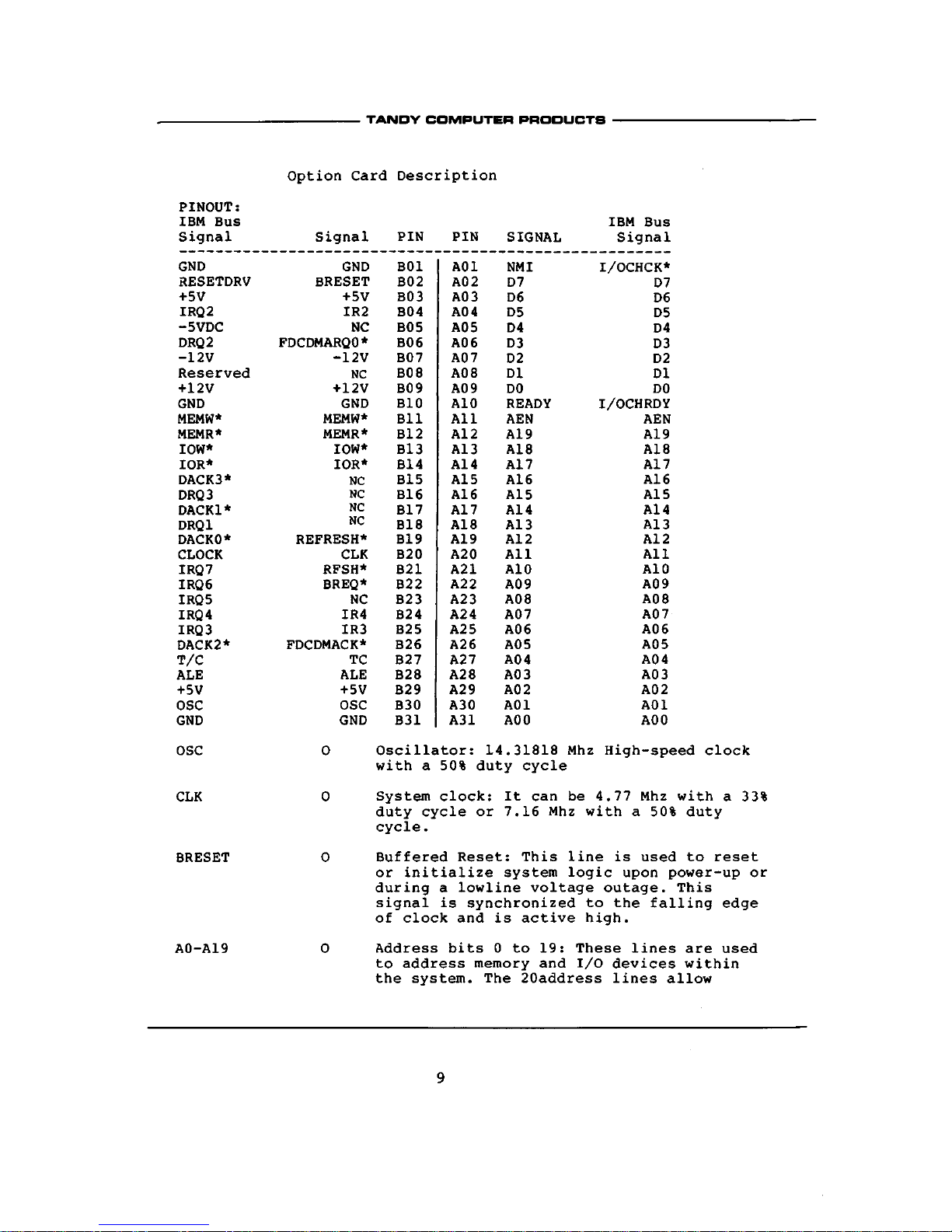
Option Card Description
PINOUT:
IBM
Bus
Signal
GND
RESETDRV
+5V
IRQ2
-5VDC
DRQ2
-12V
Reserved
+12V
GND
MEMW*
MEMR*
IOW*
IOR*
DACK3*
DRQ3
DACK1*
DRQ1
DACKO*
CLOCK
IRQ7
IRQ6
IRQ5
IRQ 4
IRQ3
DACK2*
T/C
ALE
+5V
OSC
GND
OSC
CLK
BRESET
A0-A19
Signal
GND
BRESET
+5V
IR2
NC
FDCDMARQO*
-12V
NC
+12V
GND
MEMW*
MEMR*
IOW*
IOR*
NC
NC
NC
NC
REFRESH*
CLK
RFSH*
BREQ*
NC
IR4
IR3
FDCDMACK*
TC
ALE
+ 5V
OSC
GND
0
0
0
0
PIN
B01
B02
B03
B04
B05
B06
B07
B08
B09
BIO
Bll
B12
B13
B14
B15
B16
B17
B18
B19
B20
B21
B22
B23
B24
B25
B26
B27
B28
B29
B30
B31
PIN
A01
A02
A03
A04
A05
A06
A07
A08
A09
A10
All
A12
A13
A14
A15
A16
A17
A18
A19
A20
A21
A22
A23
A24
A25
A26
A27
A28
A29
A30
A31
SIGNAL
NMI
D7
D6
D5
D4
D3
D2
Dl
DO
READY
AEN
A19
A18
A17
A16
A15
A14
A13
A12
All
A10
A09
A08
A07
A06
A05
A04
A03
A02
A01
A00
IBM
Bus
Signal
I/OCHCK*
D7
D6
D5
D4
D3
D2
Dl
DO
I/OCHRDY
AEN
A19
A18
A17
A16
A15
A14
A13
A12
All
A10
A09
A08
A07
A06
A05
A04
A03
A02
A01
A00
Oscillator: 14.31818
Mhz
High-speed clock
with a 50% duty cycle
System clock:
It can be 4.77 Mhz
with
a 33%
duty cycle
or 7.16 Mhz
with a 50% duty
cycle.
Buffered Reset: This line
is
used
to
reset
or initialize system logic upon power-up
or
during a lowline voltage outage. This
signal
is
synchronized
to the
falling edge
of clock
and is
active high.
Address bits
0 to
19: These lines
are
used
to address memory
and I/O
devices within
the system.
The
20address lines allow
•
TANDY COMPUTER PRODUCTS
10
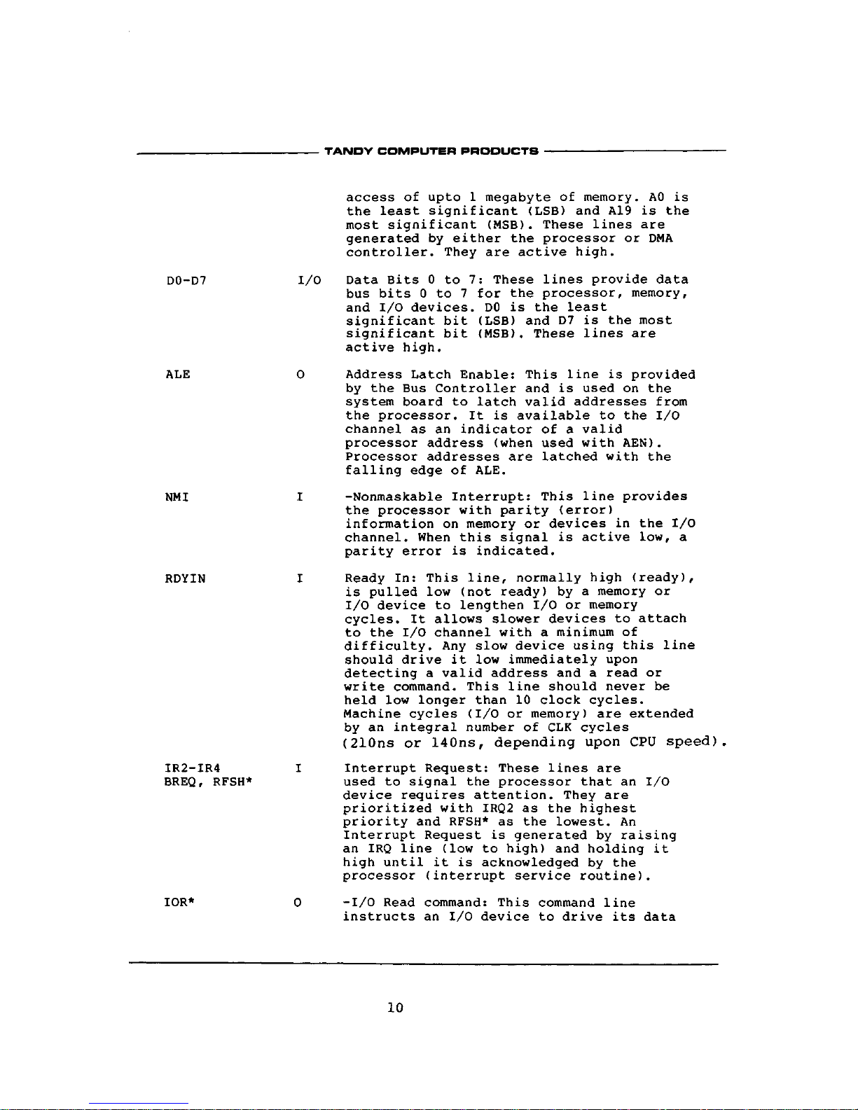
D0-D7
ALE
NMI
RDYIN
IR2-IR4
BREQr RFSH*
IOR*
I/O
0
I
I
I
0
access of upto 1 megabyte of memory. AO
is
the least significant (LSB) and A19 is the
most significant
(MSB).
These lines are
generated by either the processor or DMA
controller. They are active high.
Data Bits 0 to 7: These lines provide data
bus bits 0 to 7 for the processor, memory,
and I/O devices. DO is the least
significant bit (LSB) and D7 is the most
significant bit
(MSB).
These lines are
active high.
Address Latch Enable: This line is provided
by the Bus Controller and is used on the
system board to latch valid addresses from
the processor. It is available to the I/O
channel as an indicator of a valid
processor address (when used with AEN).
Processor addresses are latched with the
falling edge of ALE.
-Nonmaskable Interrupt: This line provides
the processor with parity (error)
information on memory or devices in the I/O
channel.
When this signal is active low,
a
parity error is indicated.
Ready In: This line, normally high
(ready),
is pulled low (not ready) by a memory or
I/O device to lengthen I/O or memory
cycles.
It allows slower devices to attach
to the I/O channel with a minimum of
difficulty. Any slow device using this line
should drive it low immediately upon
detecting a valid address and a read or
write command. This line should never be
held low longer than 10 clock cycles.
Machine cycles (I/O or memory) are extended
by an integral number of CLK cycles
(210ns or 140ns, depending upon CPU
speed).
Interrupt Request: These lines are
used to signal the processor that an I/O
device requires attention. They are
prioritized with IRQ2 as the highest
priority and RFSH* as the lowest. An
Interrupt Request is generated by raising
an IRQ line (low to high) and holding it
high until it is acknowledged by the
processor (interrupt service
routine).
-I/O Read command: This command line
instructs an I/O device to drive its data
11
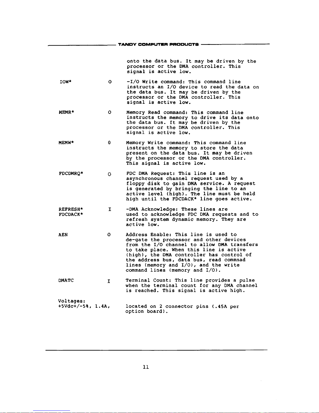
IOW*
MEMR*
MEMW*
FDCDMRQ*
REFRESH*
FDCDACK*
AEN
DMATC
Voltages:
+5Vdc+/-5%,
0
0
0
0
I
0
I
1.4A,
onto the data bus.
It
may
be
driven
by the
processor
or
the DMA controller. This
signal
is
active low.
-I/O Write command: This command line
instructs
an I/O
device
to
read the data
on
the data bus.
It
may
be
driven
by
the
processor
or
the DMA controller. This
signal
is
active low.
Memory Read command: This command line
instructs the memory
to
drive its data onto
the data bus. It may be driven
by
the
processor
or
the DMA controller. This
signal
is
active low.
Memory Write command: This command line
instructs the memory
to
store the data
present
on
the data bus. It may
be
driven
by the processor
or
the DMA controller.
This signal
is
active low.
FDC DMA Request: This line
is an
asynchronous channel request used
by a
floppy disk
to
gain DMA service. A request
is generated
by
bringing the line
to an
active level
(high).
The line must
be
held
high until the FDCDACK* line goes active.
-DMA Acknowledge: These lines are
used
to
acknowledge FDC DMA requests and
to
refresh system dynamic memory. They are
active low.
Address Enable: This line
is
used
to
de-gate the processor and other devices
from the
I/O
channel
to
allow DMA transfers
to take place. When this line
is
active
(high),
the DMA controller has control
of
the address bus, data bus, read commnad
lines (memory and I/O), and the write
command lines (memory and I/O).
Terminal Count: This line provides a pulse
when the terminal count for any DMA channel
is reached. This signal
is
active high.
located
on 2
connector pins (.45A per
option
board).
.
TANDY COMPUTER PRODUCTS
•
TANDY COMPUTER PRODUCTS
12
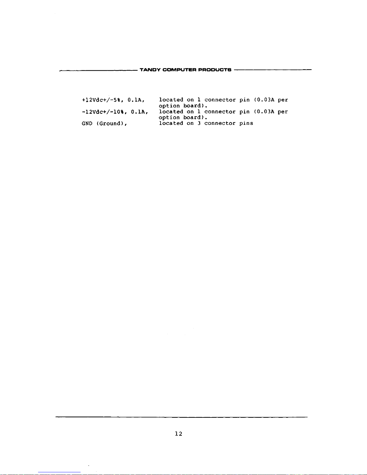
+12Vdc+/-5%,
0.1A,
-12Vdc+/-10%,
O.1A,
GND
(Ground),
located
on 1
connector pin (0.03A per
option
board).
located
on 1
connector pin
(0.0 3A
per
option
board).
located
on 3
connector pins
.
TANDY COMPUTER PRODUCTS •
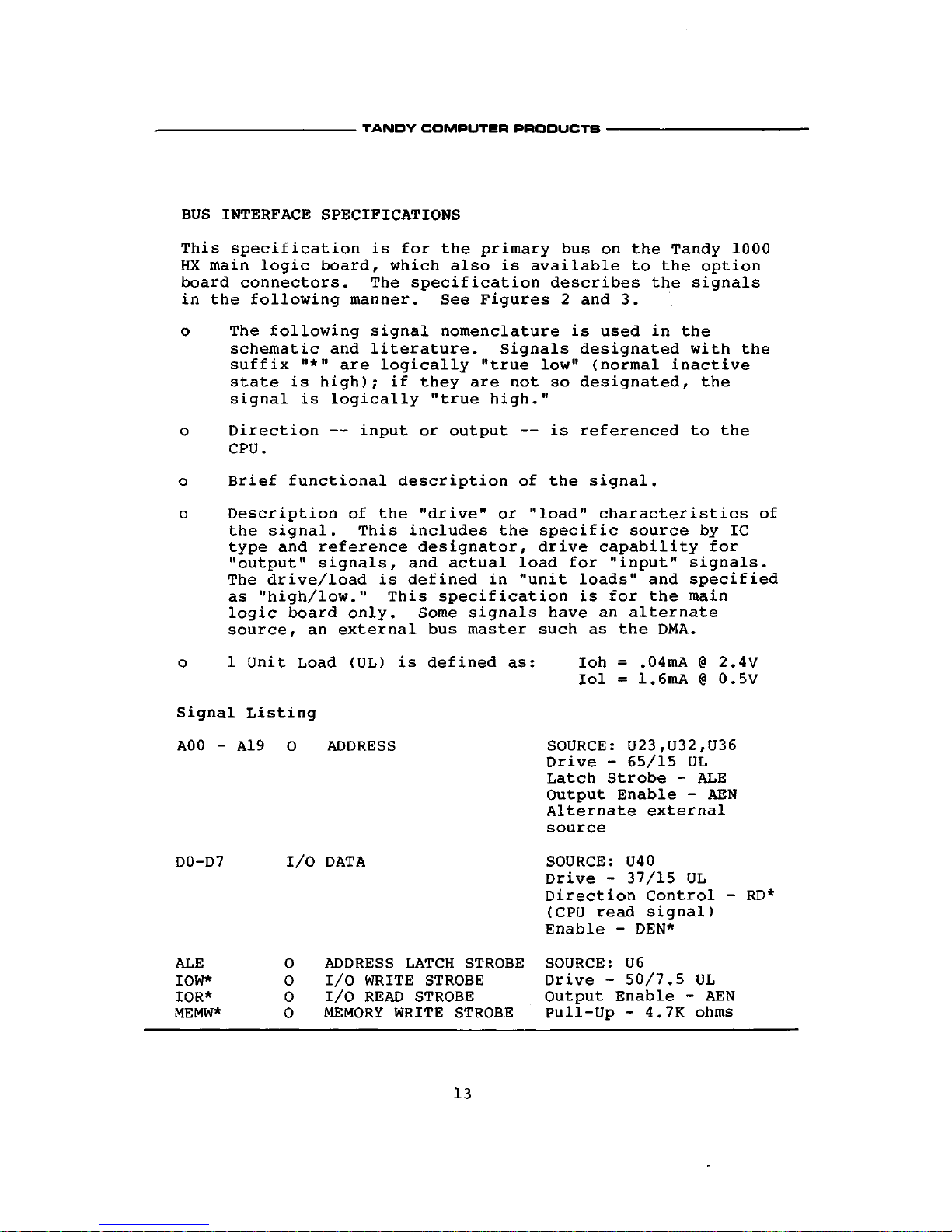
BUS INTERFACE SPECIFICATIONS
This specification
is
for the primary bus
on
the Tandy 1000
HX main logic board, which also
is
available
to
the option
board connectors. The specification describes the signals
in the following manner. See Figures
2 and 3.
o The following signal nomenclature
is
used
in the
schematic
and
literature. Signals designated with
the
suffix "*" are logically "true low" (normal inactive
state
is
high);
if
they are not
so
designated,
the
signal
is
logically "true high."
o Direction — input
or
output
— is
referenced
to the
CPU.
o Brief functional description
of
the signal.
o Description
of the
"drive"
or
"load" characteristics
of
the signal. This includes the specific source
by IC
type
and
reference designator, drive capability
for
"output"
signals,
and
actual load for "input" signals.
The drive/load
is
defined
in
"unit loads"
and
specified
as "high/low." This specification
is
for the main
logic board only. Some signals have
an
alternate
source,
an
external bus master such
as
the DMA.
o
1
Unit Load (UL)
is
defined as:
Ioh = ,04mA
@ 2.4V
Iol = 1.6mA
@ 0.5V
13
Signal
A00
-
D0-D7
ALE
IOW*
IOR*
MEMW*
Listing
A19
0
I/O
0
0
0
0
ADDRESS
DATA
ADDRESS LATCH STROBE
I/O WRITE STROBE
I/O READ STROBE
MEMORY WRITE STROBE
SOURCE:
U23,U32,U36
Drive - 65/15
UL
Latch Strobe
- ALE
Output Enable
- AEN
Alternate external
source
SOURCE:
U40
Drive - 37/15
UL
Direction Control - RD*
(CPU read signal)
Enable - DEN*
SOURCE:
U6
Drive - 50/7.5
UL
Output Enable
- AEN
Pull-Up - 4.7K ohms
•
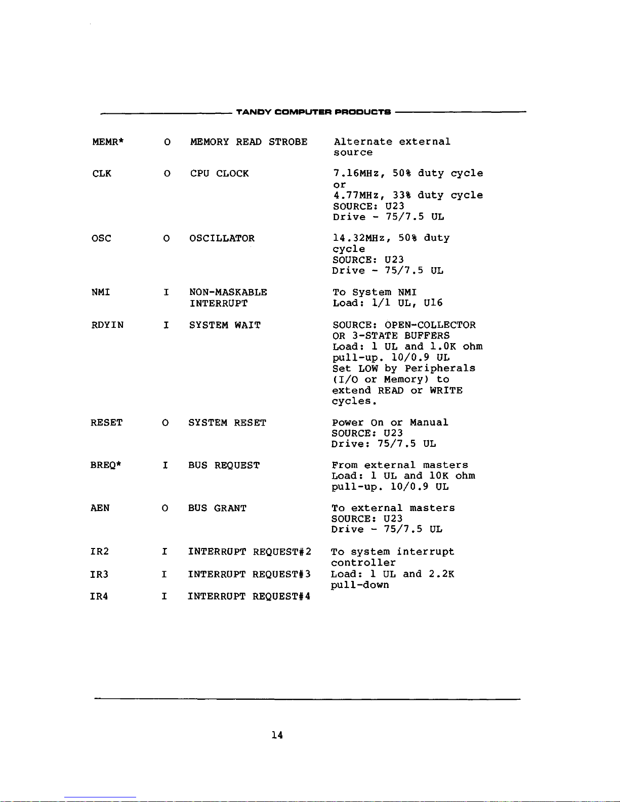
TANDY COMPUTER PRODUCTS •
14
MEMR*
CLK
OSC
NMI
RDYIN
RESET
BREQ*
AEN
IR2
IR3
IR4
0
0
0
I
I
0
I
0
I
I
I
MEMORY READ STROBE
CPU CLOCK
OSCILLATOR
NON-MASKABLE
INTERRUPT
SYSTEM WAIT
SYSTEM RESET
BUS REQUEST
BUS GRANT
INTERRUPT REQUEST*2
INTERRUPT REQUEST*3
INTERRUPT REQUEST*4
Alternate external
source
7.16MHz, 50% duty cycle
or
4.77MHz, 33% duty cycle
SOURCE:
U23
Drive - 75/7.5
UL
14.32MHz,
50% duty
cycle
SOURCE:
U23
Drive - 75/7.5
UL
To System NMI
Load:
1/1
UL,
U16
SOURCE:
OPEN-COLLECTOR
OR
3-STATE
BUFFERS
Load:
1 UL
and 1.0K ohm
pull-up.
10/0.9
UL
Set LOW
by
Peripherals
(I/O
or
Memory)
to
extend READ
or
WRITE
cycles.
Power
On or
Manual
SOURCE:
U23
Drive:
75/7.5
UL
From external masters
Load:
1 UL
and 10K ohm
pull-up.
10/0.9
UL
To external masters
SOURCE:
U23
Drive - 75/7.5
UL
To system interrupt
controller
Load:
1 UL
and 2.2K
pull-down
•
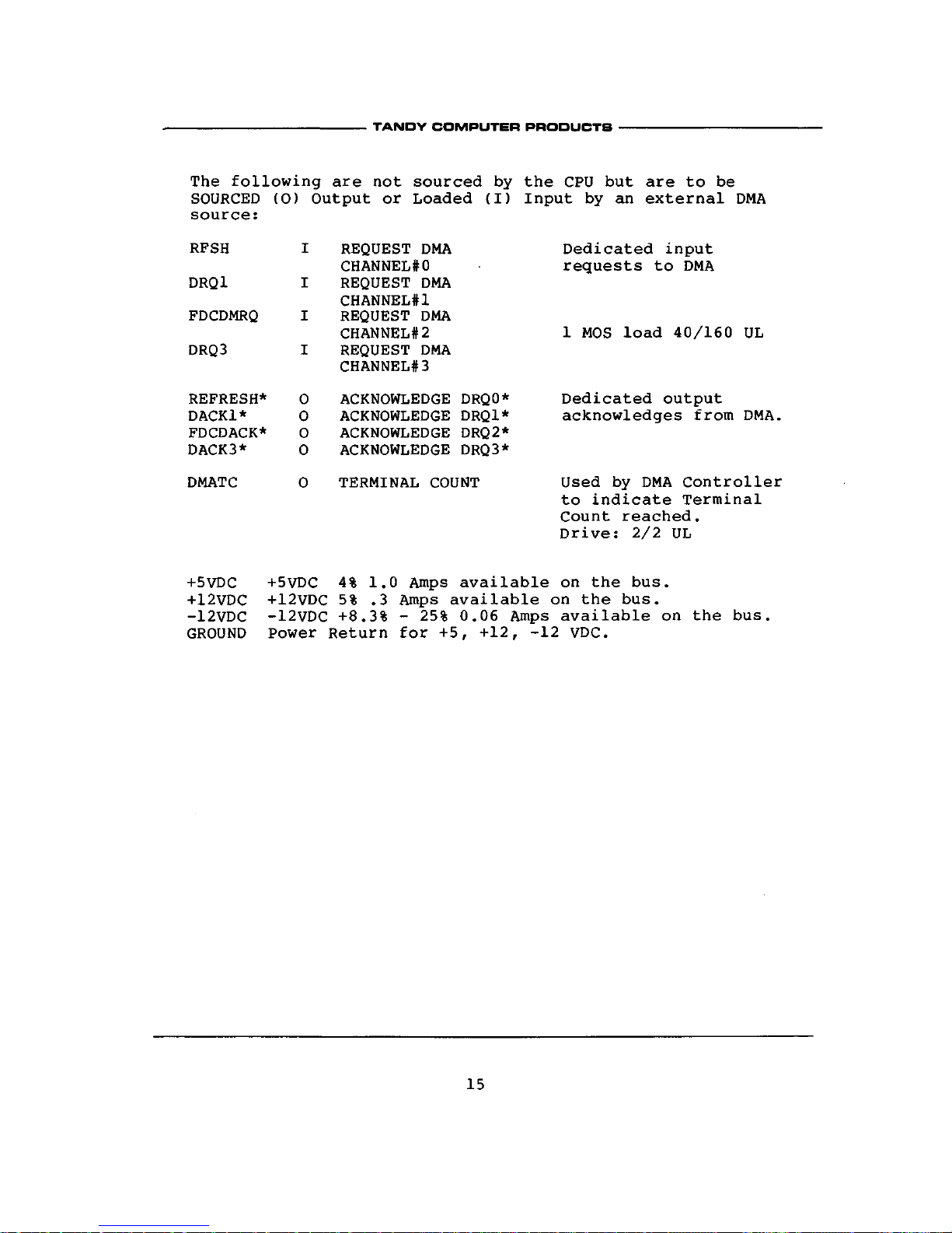
TANDY COMPUTER PRODUCTS •
The following are not sourced
by
the CPU but are
to be
SOURCED (0) Output
or
Loaded (I) Input
by an
external
DMA
source:
15
RFSH
DRQ1
FDCDMRQ
DRQ3
REFRESH*
DACKl*
FDCDACK*
DACK3*
DMATC
+5VDC
+12VDC
-12VDC
GROUND
I
I
I
I
0
0
0
0
0
+5VDC
+12VDC
-12VDC
Power
REQUEST DMA
CHANNEL*0
REQUEST DMA
CHANNEL*1
REQUEST DMA
CHANNEL*2
REQUEST DMA
CHANNEL*3
ACKNOWLEDGE DRQO*
ACKNOWLEDGE
DRQl*
ACKNOWLEDGE
DRQ2*
ACKNOWLEDGE
DRQ3*
TERMINAL COUNT
Dedicated input
requests
to
DMA
1 MOS load 40/160
UL
Dedicated output
acknowledges from DMA.
Used
by
DMA Controller
to indicate Terminal
Count reached.
Drive:
2/2
UL
4%
1.0
Amps available
on
the bus.
5%
.3
Amps available
on
the bus.
+8.3% - 25% 0.06 Amps available
on
the bus.
Return for +5, +12, -12 VDC.
•
TANDY COMPUTER PRODUCTS
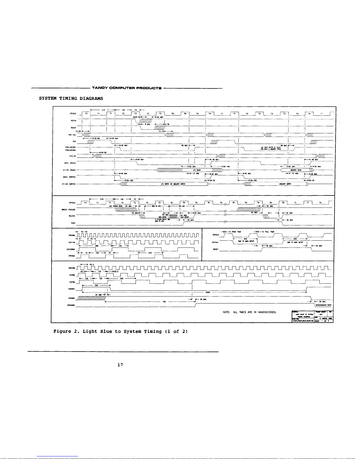
SYSTEM TIMING DIAGRAMS
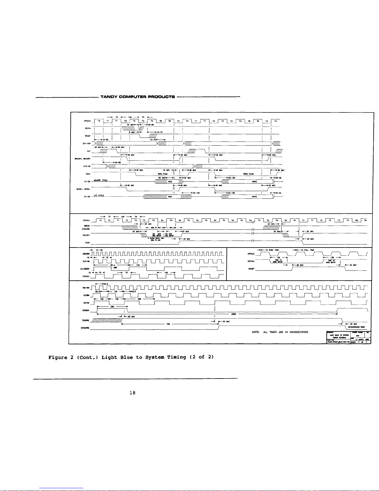
Figure 2. Light Blue to System Timing (1 of
2)
17
.
TANDY COMPUTER PRODUCTS
Figure 2 (Cont.) Light Blue
to
System Timing (2
of 2)
18
•
TANDY COMPUTER PRODUCTS
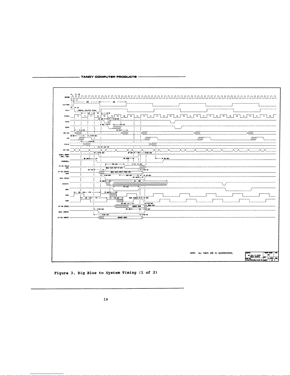
Figure 3. Big Blue
to
System Timing
(1 of 2)
19
•
TANDY COMPUTER PRODUCTS •
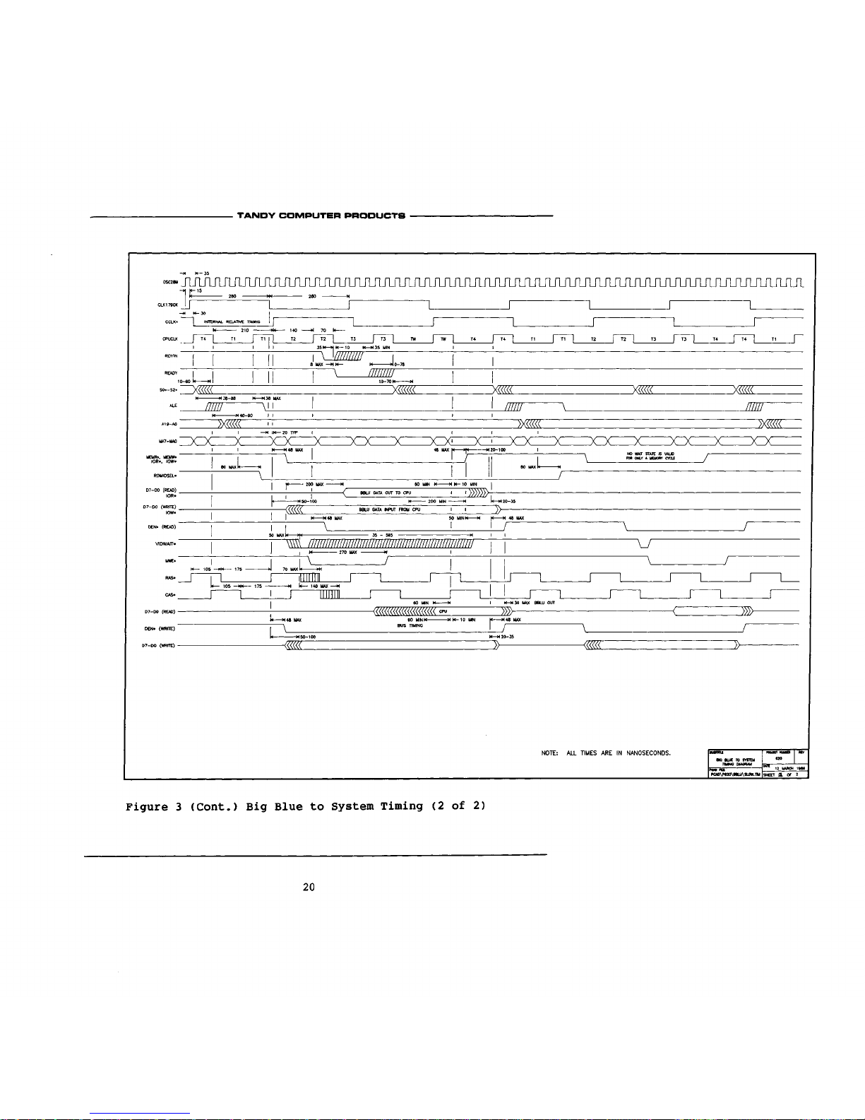
Figure 3 (Cont.) Big Blue
to
System Timing
(2 of 2)
20
TANDY COMPUTER PRODUCTS •
THEORY
OF
OPERATION
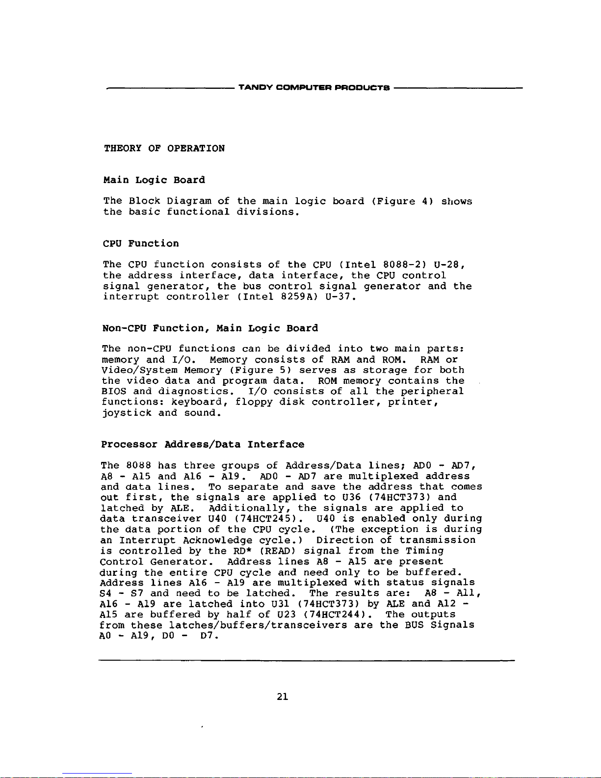
Main Logic Board
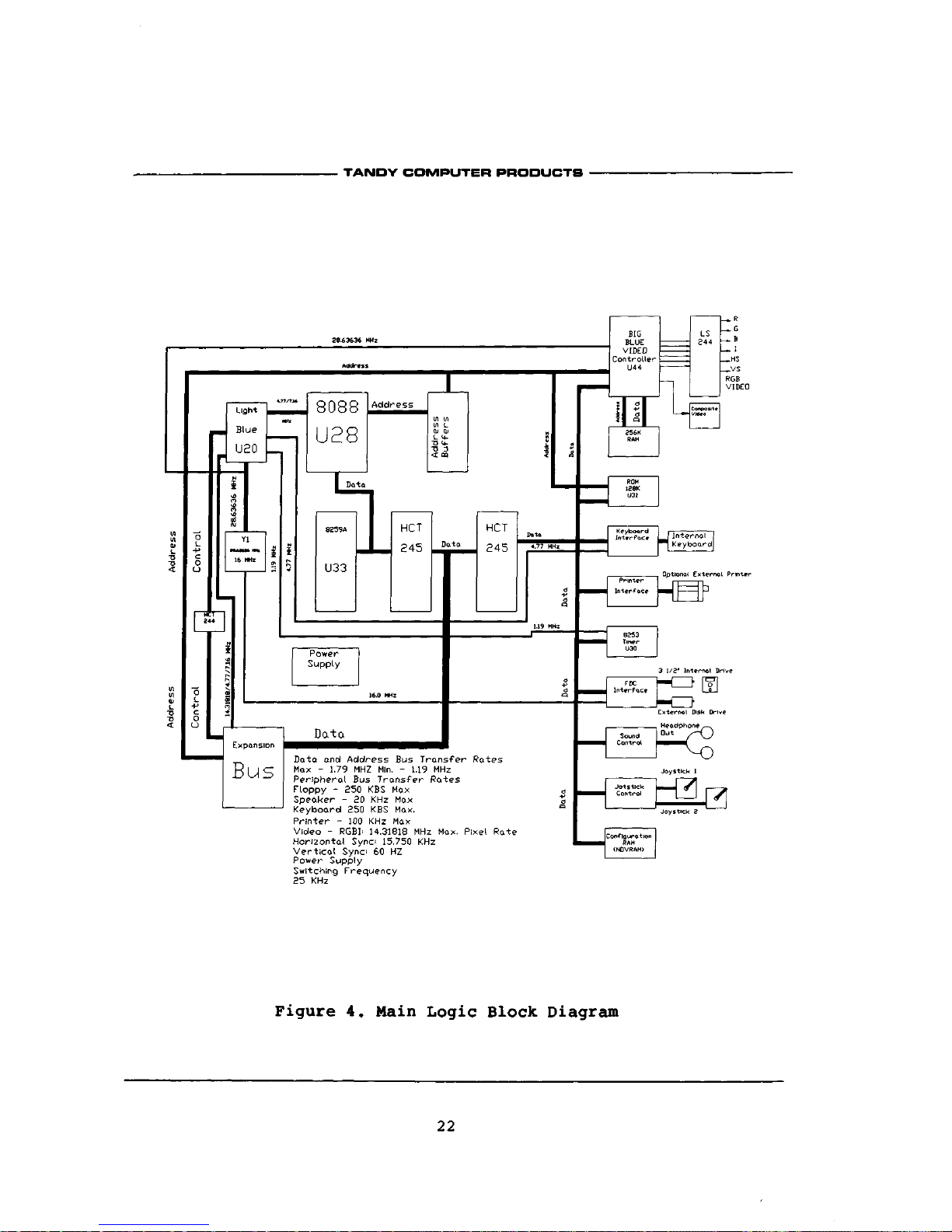
The Block Diagram of the main logic board (Figure 4) shows
the basic functional divisions.
CPU Function
The CPU function consists
of
the CPU (Intel 8088-2) U-28,
the address interface, data interface, the CPU control
signal generator, the bus control signal generator and
the
interrupt controller (Intel 8259A) U-37.
Non-CPU Function, Main Logic Board
The non-CPU functions can
be
divided into two main parts:
memory and I/O. Memory consists
of
RAM and ROM. RAM
or
Video/System Memory (Figure 5) serves
as
storage for both
the video data and program data. ROM memory contains
the
BIOS and diagnostics.
I/O
consists
of
all the peripheral
functions:
keyboard, floppy disk controller, printer,
joystick and sound.
Processor Address/Data Interface
The 8088 has three groups
of
Address/Data lines;
ADO -
AD7,
A8 - A15
and
A16 - A19.
ADO -
AD7 are multiplexed address
and data lines.
To
separate and save the address that comes
out first, the signals are applied
to
U36 (74HCT373)
and
latched
by
ALE. Additionally, the signals are applied
to
data transceiver U40
(74HCT245).
U40
is
enabled only during
the data portion
of
the CPU cycle. (The exception
is
during
an Interrupt Acknowledge cycle.) Direction
of
transmission
is controlled
by
the RD* (READ) signal from the Timing
Control Generator. Address lines
A8 -
A15 are present
during the entire CPU cycle and need only
to be
buffered.
Address lines A16 - A19 are multiplexed with status signals
S4
- S7
and need
to be
latched. The results are:
A8 -
All,
A16 - A19 are latched into U31
(74HCT37 3)
by
ALE and A12
-
A15 are buffered
by
half
of
U23
(74HCT244).
The outputs
from these latches/buffers/transceivers are the BUS Signals
A0 - A19,
DO - D7.
21
.
TANDY COMPUTER PRODUCTS
Figure
4.
Main Logic Block Diagram
22
•
TANDY COMPUTER PRODUCTS
Figure
5.
Memory Map
23
.
TANDY COMPUTER PRODUCTS
CPU Control Signal Generation
The 8088 CPU uses a 4.77 (7.16) MHz clock with a special
duty cycle (4.77
-»
33% high, 67% low, - 7.16
-»
50% high,
50%
low). This clock
is
produced
by
the Timing Control
Generator. The Timing Control Generator receives a 28.63636
MHz input clock and divides
it by 6 to
produce 4.77
MHz
CPUCLK
or by 4 to
produce 7.16 MHz CPUCLK, and
by 24 to
produce D4CLK (1.193 MHz).
In
addition to being used
by
the
control signal logic, the clocks are buffered
by
U20
(74HCT244) for the bus signals OSCY (14 MHz), CLKY (CPU
clock:
4.77/7.16
MHz). (See the Bus Interface
Specification).
The RESET signals (RESET and BRESET) originate
at
U20
(Timing Control Generator) which synchronizes the input
RSTIN*. RSTIN* originates from C132 which is discharged
to
0 volts
by
diode CR2 when the power
is
off.
The READY circuit synchronizes the system "ready" signals
with the CPU clock and generates the CPU input READY.
If a
function needs one
or
more "wait" states added
to its
access,
it
must set the RDYIN line low. From the main logic
board, RDYIN
is
set low
by
the sound
IC
for
32
extra "wait
states"
and the video/system memory sets RDYIN low for
typically one
or
two "wait" cycles. The READY circuit
of
the Timing Control Generator (U20)
is
operated
in the
non-asynchronous mode; i.e. two sequential edges
of
clock
(a
rising edge first) are required
to
set the READY signal
true.
RDYIN is pulled-up
by
R20.
IFL Equations
U16 Buffer Control Checksum: FF6C
Inputs Outputs
PIN
1 =
!mio PIN
7 =
!fdcack PIN 15 = Idisnmi
PIN
2 =
Imemr PIN
8 =
!ior Pin
16 =
!romcs
PIN
3 =
al9 PIN
9 =
!refresh PIN 17 = Ibufenb
PIN
4 =
al8 PIN 11 = nmien PIN 18 = Ibufdir
PIN
5 =
al7 PIN 13 = nmi
PIN
6 =
Imemios PIN 14 = Iromdis
24
TANDY COMPUTER PRODUCTS
Equations:
/** Logic Equations
**/
disnmi = Inmien
#
Inmi;
romcs
=
memr & 'refresh & al9 & al8 & al7 & Iromdis;
bufenb = Imemios & romcs
# memios & fdcack;
bufdir = memr & imio & !fdcack
# memr & Imio & memios
# memr & !mio
& ior
# mio
& ior
# ior & fdcack & Imemios & Imemr;
System Control Signal Generation
The Timing Control Generator (U20) provides the timing
strobes required
by
the system. These include LIOW*, LIOR*,
LMEMW*, LMEMR*, LALE, LDEN* and LIO/M*. They are buffered
by
U6 and become IOW*f IOR*, MEMW*, MEMR*f ALE, DEN*
and
IO/M*. All external devices, except the 8259A Interrupt
Controller, are buffered
by a
HCT244 (U6) that
is
controlled
by the DEN* signal. Since the 8259A is not buffered,
the
DEN*
signal must remain inactive during access
to
the 8259A.
The signals LIOW*, LIOR*, LMEMW*, LMEMR*, LALE, LDEN*
and
LIO/M* are synthesized 8088 status signals SO*, Si*, S2*
and
INTCS*
(8259A chip
select).
See Figure
6.
Bus Specification
Specifications for the bus will include the expansion
connector pin/signal assignments and the signal
characteristics. Refer
to
the Expansion
I/F
Connector
diagram. See Figure
7.
25

•
TANDY COMPUTER PRODUCTS
Figure 6. System Control Timing
26

•
TANDY COMPUTER PRODUCTS
Figure 7. Expansion
I/F
Connector
27

•
TANDY COMPUTER PRODUCTS -
Interrupt Function
The 8088 supports
two
types
of
interrupts: maskable
(by the
CPU,
INT) and
non-maskable
(NMD. See
Figure
8. The
8259A
Interrupt Controller
is the
source
of the INT for the
8088.
The 8259A
has
eight interrupt inputs controlled through
software commands.
It can
mask (disable)
and
prioritize
(arrange priority)
to
the
inputs which
can
generate
INT.
These eight interrupts
are:
The
NMI
interrupt
is
not
maskable
by
the CPU but
it
can
be
enabled/disabled
by
hardware.
The
enable
is at
Port 00A0
Bit
7. The
enable
is
cleared
by
RESET. There
is
no
specific function assigned
to NMI and
it is
available
on
the
bus.
28
#0
#1
#2
#3
#4
#5
#6
#7
Timer Channel
0
Keyboard
Hard Disk Controller
Comm
2
Comm
1
Vertical Sync
Disk Controller, Floppy
Printer
Software Timer
Keyboard Code Received
Optional Function, Interrupt
on Bus
Optional Function, Interrupt
on Bus
Optional Function, Interrupt
on Bus
Software Timer for Video
Ready
to
Receive/Transmit
Data
Data Transmission Complete

•
TANDY COMPUTER PRODUCTS
8259A INTERRUPT CONTROLLER
INTERRUPT
NMI
0
1
2
3
4
5
6
7
FUNCTION
AVAILABLE ON BUS
8253 TIMER CH 0 (REFRESH)
KEYBOARD
HARD DISK
SECONDARY COMM.
PRIMARY COMM.
VERTICAL SYNC.
FLOPPY DISK CONTROLLER
PARALLEL PORT
Figure
8.
Interrupt Structure
29
•
TANDY COMPUTER PRODUCTS •
Bus Interface
The interface to the main bus is divided into three parts:
address/control strobes, memory data and I/O data.
The
address/control strobe part (AO - A19, MEMR*, MEMW*, IOR*,
IOW*) is shared by both the I/O and the memory sections.
The address buffers are U23, U32 and U36. One function of
the address bus is the select logic for each of the
functions.
U27 decodes all the I/O chip selects except
those for the Video/System Memory I/O ports which are
decoded by U31. The memory selects are decoded by U31 except
the ROMCS*, which is decoded by U16. The I/O data
transceiver is U44 with its output enable and direction
control decoded by U16.
Keyboard / Timer / Sound Circuits
The Keyboard Interface consists of an 8048 CPU (U9) and
a
Keyboard Controller
(U13),
which is a Custom Gate Array.
Included in U13 is an 8255 programmable peripheral interface
equivalent design. It has three 8 bit parallel ports, A,
B
and C. Port A is configured as an input port and is used
for keyboard data. Port B is configured as an output port
and is used for control signals for the sound, keyboard and
timer functions. Port C is split into 4 inputs, including
the timer channel and #2 monitor and 4 outputs including the
keyboard/multifunction interface signals.
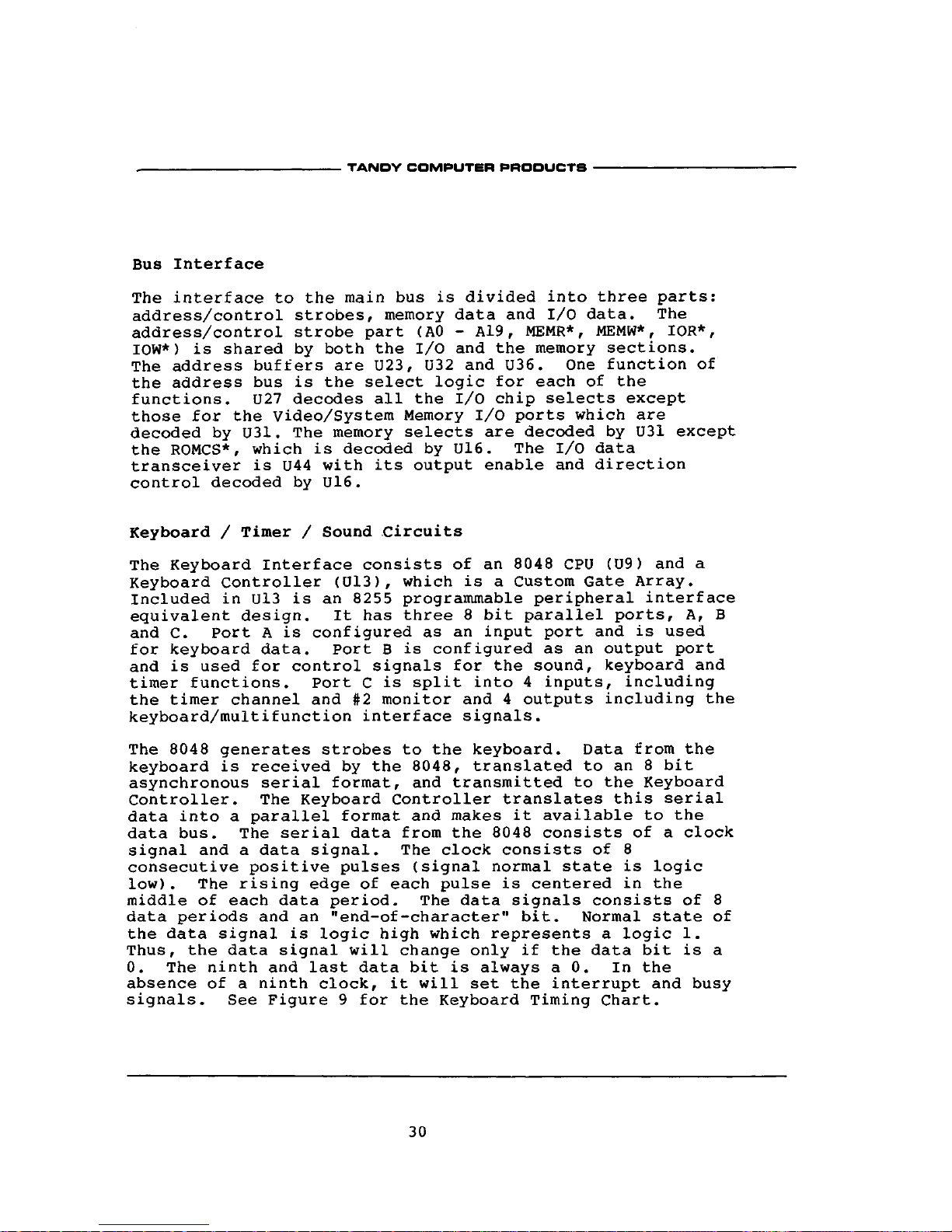
The 8048 generates strobes to the keyboard. Data from the
keyboard is received by the
8048,
translated to an 8 bit
asynchronous serial format, and transmitted to the Keyboard
Controller. The Keyboard Controller translates this serial
data into a parallel format and makes it available to the
data bus. The serial data from the 8048 consists of a clock
signal and a data signal. The clock consists of
8
consecutive positive pulses (signal normal state is logic
low).
The rising edge of each pulse is centered in the
middle of each data period. The data signals consists of
8
data periods and an "end-of-character" bit. Normal state of
the data signal is logic high which represents a logic 1.
Thus,
the data signal will change only if the data bit is
a
0. The ninth and last data bit is always a 0. In the
absence of a ninth clock, it will set the interrupt and busy
signals.
See Figure 9 for the Keyboard Timing Chart.
30
TANDY COMPUTER PRODUCTS •
Figure 9. Keyboard Timing Chart
31
.
TANDY COMPUTER PRODUCTS
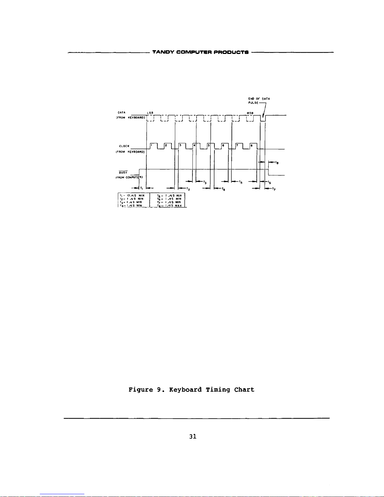
Timer Function
The Timer
is an
8253 Timer/Counter consisting
of
three
independent counters. The clock for all three counters
is
1.19
25
MHz. The gates for counters
#0
and #1
are
permanently "on". The gate for counter
#2 is
controlled
by
a bit
of
the keyboard interface (8255 Port
B).
The output
of counter
#0
is dedicated
to
system interrupt
#0
(8259 IRO)
for software timing functions. The output
of
counter
#1 is
dedicated
to
the REFRESH function. When the optional
DMA/Memory board
is
installed, DMA channel
#0
is used for
refreshing the RAM memory. Counter
#1
sets RFSHRQ* (DRQO)
every
15
micro-seconds
to
initiate a single "dummy" memory
read. The output
of
counter
#2 is
routed
to
the sound
circuit and into the 8255 Port C for monitoring
by
the CPU.
See Figure 10.
Sound Function
The sound function consists
of an
internal and
an
external
sound circuit. These are directly connected
to
the
Headphone Output via U5. The source of the sound
frequencies
is
U19, a Complex Sound Generator. Internally,
U19 has three programmable tone generators and a noise
generator. The frequency and output level
of
each
is
controlled
by
software. The four internal generators are
summed with
an
external input into a single output.
The
external source
is
from the 8253 counter
#2
(programmable
frequency and fixed
amplitude).
It is
one
of
two selectable
sources for the external audio out signal. This signal
is
intended as
an
input into
an
external earplug. The two
sound frequency sources are:
1. Complex sound generator U19.
2.
The 8253 counter
at
channel
2.
The output driver for Audio Out is U5. See Figure 11.
32
.
TANDY COMPUTER PRODUCTS •
8253-5 TIMER
Figure 10. System Timer 8253-5
33

TANDY COMPUTER PRODUCTS
Figure 11. Sound Functional Block Diagram
34

•
TANDY COMPUTER PRODUCTS
Joystick Interface
The joystick interface converts positional information from
hand-held joysticks (1 or 2) into CPU data. Each joystick
provides 1 or 2 push-buttons and X, Y position for a total
of 4 bits each. Two joysticks can be used. The joystick
handle is connected to two potentiometers mounted perpendicular to each other; one for X position, one for Y position.
Through the cable, the main logic board applies +5 VDC to
one side and ground to the other of the
pots.
The pot wiper
is the position signal: a voltage between 0 and +5 VDC.
This signal is applied to one input of a comparator U24.
The other comparator input is the reference signal (a ramp
between 0.0 to +5.0 volts.) When the position signal
is
equal to or greater than the reference signal, the
comparator output goes true. This comparator output is the
X or Y position data bit. The ramp is reset to 0.0 VDC
whenever a "write" is made at Port 200/201 Hex. The IOW*
signal turns on Q2, which discharges C129 to 0.0 volts.
When Q2 is turned off, Ql, R22, R28, R35, and CR3 create
a
constant-current source that linearly charges C129 to +5.0
VDC in 1.12 milliseconds. The joystick information is
"read" by the CPU at Port 200/201 Hex through U26.
See
Figure 12.
Printer Interface
The printer interface is totally contained in a custom Gate
Array U37 and is shown in Figure 13. Functionally, the
printer interface consists of an output data latch (write
port 378) and accompanying input data buffer. The data
written to the output port latch may be read at port 37A.
The input data from the printer connector may be read back
at port 378. The input buffer is for reading printer input
signals (read port 379), I/O address decoding, data
transceiver, and interrupt logic. The interrupt is
logically connected to ACKNOWLEDGE* if interrupts are
enabled (37A Bit 4).
35

•
TANDY COMPUTER PRODUCTS
PROGRAMMING CONSIDERATIONS
IOR's
@
REGULAR INTERVALS
ONCE TRIGGERED BY SOFTWARE THE
INTERGRATOR CIRCUIT PRODUCES A PULSE
THE DURATION OF WHICH IS DEPENDENT ON
JOYSK POSITION.
Figure 12. Joystick
I/F
36

•
TANDY COMPUTER PRODUCTS •
Figure 13, Printer Block Diagram
Pin Definitions
of
the FDSL:
Pin
1.
2.
3.
4.
5.
6.
7.
8.
9.
10.
11.
13.
14.
15.
16.
17.
18.
19.
20.
21.
22.
23
Name
CLK16M
WCK
FDCCLK
RDDATA*
RDD
RDW
FRES/S
RW*/SEEK
TRKO*
F/TRKO
STEP*
WRDATA*
WRE
WRD
PS1
PSO
FDCDMRQ*
FDCINT
DRQ
DMA/INTE
INT+
SWITCH
Type
Input
Output
Output
Input
Output
Output
Input
Input
Input
Output
Output
Output
Input
Input
Input
Input
Output
Output
Input
Input
Input
Input
Description
Raw Clock
16 MHz
Write Clock
FDC Clock
Serial Data From
FDD
Serial Data From
FDC
Read Data Window
Step Pulses
to
Move the Head
Specifies Seek Mode When High
From FDD Indicating Head @ Track
0
To FDC Indicating Head @ Track
0
Moves Head
Of FDD
Serial Data
To FDD
Write Enable
Write Data From
FDC
Write Precompensation Status
Write Precompensation Status
DRQ Delayed
By 1
usec.
Interrupt Request
FDC DMA Request
DMA Request
& FDC
Interrupt Enable
Interrupt Request Generated
By FDC
0 = Low Density Drive
1 = High Density Drive
Table
1.
37

•
TANDY COMPUTER PRODUCTS
Floppy Disk Controller Interface
The FDC interface consists
of
the NEC UPD765A controller
and Custom FDC Support Chip
(FDSL).
The clocks
are
generated
by
the FDSL. The FDSL receives a raw clock
of 16
MHz.
The clock outputs
to
the FDC Controller consist
of
Write Clock (WCK)
at
250 nsec every 2 usec, and FDC Clock
(FDCCLK)
at
4.00 MHz which
is
applied
to
the FDC Controller
for its internal processor clock (CLK pin 19).
The FDSL receives the step signal (FRES/S) from the
FDC
Controller and generates the step pulses (STEP*)
to
the FDD
to move the heads. The FDSL receives the Track 0 signal from
the FDD (TRKO*) and relays
it to
the FDC Controller with
the
F/TRKO
signal.
The FDSL also handles DMA Request
and
Interrupt
Enable (DMA/INTE)
as
well
as
Interrupt Request (INT+)
generated
by
the FDC Controller. The FDSL receives DMA
Request (DRQ) from the FDC Controller and generates
a 1
usec
delayed DMA Request (FDCDMRQ*)
to
the Expansion Bus.
The FDSL converts Serial Read Data (RDDATA*) from the FDD
into Serial Read Data (RDD) and Read Data Window (RDW)
and
sends
it on to
the FDC Controller.
The FDC Controller supplies Write Enable
(WRE),
Serial Data
(WRD) and Write Pre-compensation (PSO,
PSD to
the FDSL
to
produce Serial Output Data (WRDATA*)
to
the FDD. The
FDC
Controller also generates the (RW*/SEEK) signal
to
the FDSL
to put the FDC
in
Seek Mode. (High signal
to
indicate Seek
Mode).
Pin Definitions for the FDSL are found
in
Table 1.
Pin
definitions for the UPD765A may
be
found
in
the Device
Specifications Section.
38

•
TANDY COMPUTER PRODUCTS
Video System Logic
A major block of the Tandy 1000 HX is the video interface
circuitry.
A
block diagram of the video controller
circuit is shown in Figure 14. This custom part contains
all of the logic necessary to generate an IBM compatible
color video display. The video interface logic
consists of the 84 pin custom video circuit,
8 -
64K
X 4
RAMs, a 74LS244 buffer, and associated circuitry for
generation of composite video.
The Tandy 1000 HX video interface circuitry controls 256K of
memory. See Video System Memory Map, Figure 15. This RAM is
shared by the CPU and the video. Normally, the video only
requires 16K or 32K for the video screen and the remainder
of the 256K is available for system memory
uses.
The Tandy 1000 HX video interface custom circuit is composed
of a 6845 equivalent design, dynamic RAM address generation/
timing (see Figure
16.),
and video attribute controller
logic.
Normal functioning of the video interface custom circuit is
as follows: After the 6845 is programmed with a correct; set
of operating values (see Table 2), the address inputs to the
dynamic RAMs are generated by a 4:1 multiplexer. This MUX
switches between video (6845) addresses and CPU addresses as
well as between row and column addresses. In addition, the
video interface chip provides the RAM timing signals and
generates a wait signal to CPU for proper synchronization
with the video RAM access cycles.
The outputs from the RAM chips are only connected to the
video interface custom circuit, so all CPU read/write
operations are buffered by this part. During a normal
display cycle, video data from the RAM chips is first
latched in the Video Attribute latch and the Video Character
latch.
The video interface requires a memory organization
of 64K X 16 and will latch 16 bits of memory during each
access to RAM. From the output of the two latches, the
data is supplied to the character ROM for the Alpha modes
or to the shift registers for graphics modes.
A
final 2:1
MUX is used to switch between foreground or background in
the alpha mode.
From the 2:1 MUX, the RGBI data is combined with the PC
color select data and latched in the Pre-Palette latch.
This latch synchronizes the RGBI data before it is used to
address the palette.
39

•
TANDY COMPUTER PRODUCTS
Figure 14. Video Controller Block Diagrcun
40

.
TANDY COMPUTER PRODUCTS
Figure
15.
Video System Memory
Map
41

.
TANDY COMPUTER PRODUCTS •
Main System Board Ram Timing Specification
AC Operating Conditions and Characteristics
Parameter
Random Read
or
Write Cycle Time
Read Write Cycle Time
Access Time from Row Address
Strobe
Access Time from Column Address
Output Buffer and Turn-off Delay
Row Address Strobe Precharge Time
Row Address Strobe Pulse Width
Column Address Strobe Pulse Width
Row Address Setup Time
Row Address Hold Time
Column Address Setup Time
Column Address Hold Time
Transition Time (Rise and Fall)
Read Command Setup Time
Read Command Hold Time
Read Command Hold Time Referenced
to RAS
Write Command Hold Time
Write Command Hold Time Referenced
to RAS
Write Command Pulse Width
Write Command
to
Row Strobe Lead
Time
Write Command
to
Column Strobe
Lead Time
Data
in
Setup Time
Data
in
Hold Time
Data
in
Hold Time Referenced
to
RAS
Column
to
Row Strobe Precharge
Time
RAS Hold Time
Refresh Period
WRITE Command Setup Time
CAS
to
WRITE Delay
RAS
to
WRITE Delay
CAS Hold Time
Symbol
tRC
tRWC
tRAC
tCAC
tOFF
tRP
tRASl
tCAS
tASR
tRAH
tASC
tCAH
tT
tRCS
tRCH
tRRH
tWCH
tWCR
tWP
tRWL
tCWL
tDS
tDH
tDHR
tCRP
tRSH
tRFSH
twcs
tCWD
tRWD
tCSH
Min.
279
279
—
—
0
100
170
130
0
20
0
35
—
0
0
0
35
95
35
45
45
0
35
95
0
85
—
0
45
120
200
Max.
—
—
200
100
30
—
—
—
—
—
—
—
50
—
—
—
—
—
—
—
—
—
——
—
2.0
—
—
—
——
Units
ns
ns
ns
ns
ns
ns
ns
ns
ns
ns
ns
ns
ns
ns
ns
ns
ns
ns
ns
ns
ns
ns
ns
ns
ns
ns
ns
ns
ns
ns
ns
Figure 16. Main System Board RAM Timing Specification
42

•
TANDY COMPUTER PRODUCTS •
PROGRAMMING TABLE FOR THE 6845 All Values
in
Hex (Decimal)
101
02
03
04
05
06
07
Ob
09
11
12
13
Register
Address
Horizontal
Displayed
Horizontal
Sync Position
Horizontal
Sync Width
Vertical Total
Vertical
Total Adjust
Vertical
Displayed
Vertical
Sync Position
Interlace Mode
Max Scan
Line Address
Cursor Start
Cursor End
Start
Address (High)
Start
Address (Low)
|
40 x 2b
Alpha
3d (56)
28
2D
0b
1C
01
19
1A
02
0b
06
07
00
00
(40)
(45)
(8)
(28)
(1)
(25)
(26)
(2)
(8)
(6)
(7)
(0)
(0)
80 x 25
Alpha
71 (113)
50
59
10
ic
01
19
1A
02
08
06
07
00
00
(80)
(89)
(16)
(2b)
(1)
(25)
(26)
(2)
(8)
(6)
(7)
(0)
(0)
Low Res.
Graphics
3b (56)
28
2D
08
7F
06
64
70
02
01
06
07
00
00
(40)
(45)
(8)
(127)
(6)
(100)
(112)
(2)
(1)
(6)
(7)
(0)
(0)
High Res.
Graphics
71 (113
50
59
10
3F
06
32
38
02
03
06
07
00
00
(80)
(89)
(16)
(63)
(6)
(50)
(56)
(2)
(3)
(6)
(7)
(0)
(0)
40 x 25
Alpha
38 (56)
28
2D
08
IF
06
19
ic
02
07
06
07
00
00
(40)
(45)
(8)
(31)
(6)
(25)
(28)
(2)
(7)
(6)
(7)
(0)
(0)
80 x 25
Alpha
71 (113)
50
59
10
IF
06
19
IC
02
07
06
07
00
00
(80)
(89)
(16)
(31)
(6)
(25)
(28)
(2)
(7)
(6)
(7)
(0)
(0)
Low Res
Graphics
38 (56)
28
2D
08
7F
06
64
70
02
01
06
07
00
00
(40)
(45)
(8)
(127)
(6)
(100)
(112)
(2)
(1)
(6)
(7)
(0)
(0)
High Res
Graphics
71 (113)
50
59
10
3F
06
32
38
02
03
06
07
00
00
(80)
(89)
(16)
(63)
(6)
(50)
(56)
(2)
(3)
(6)
(7)
(0)
(0)
Monitor Mode
Table
2
43
•
TANDY COMPUTER PRODUCTS •
The palette mask MUX
is
used
to
switch between incoming RGBI
data and the palette address register. During a CPU write
to the palette, this address register selects one
of
the
16
palette locations. Also, the palette mask MUX allows any
of
the input RGBI bits
to be
set
to
zero.
The palette allows the
16
colors
to be
remapped
in
any
desired organization. Normally the pallete
is
set
for
a 1:1 mapping (red = red, blue = blue, etc.) for
PC
compatibility. However, instantly changing the on-screen
colors
is a
very powerful tool for animation
or
graphics
programs.
After the palette, the RGBI data
is
resynchronized
in the
Post Palette register. The final logic before the RGBI data
is buffered off the chip
is
the Border MUX. This MUX
allows the Border
to be
replaced with any color selected
by
the border color latch. This latch
is
normally disabled
in
PC modes, but
it is
used
in
all PCjr modes.
44

•
TANDY COMPUTER PRODUCTS •
1/0 MAP SUMMARY
Block
0000-001F
0020-003F
0040-005F
0060-007F
0080-009F
00A0-00BF
00C0-00DF
00E0-01FF
0200-020F
0210-031F
0320-032F
0330-036F
0370-037F
0380-03CF
03D0-03DF
03E0-03EF
03F0-03FF
0400-FFFF
Usage
0000-000F
0020-0021
0040-0043
0060-0063
0080-0083
00A0
OOCO-OOCl
0200-0201
0378-037B
All
03Fl,03F2,F4,F5
03F8-03FF
Function
Optional DMA Function
Interrupt Controller
Timer
PIO Function
Optional DMA Page
Register
NMI Mask Register
Sound Generator
Reserved
Joystick Interface
Reserved
Reserved Hard Disk
Not Assigned
Printer
Not Used
System Video
Reserved
Floppy Disk Controller
Optional COM Port
Not Usable
45
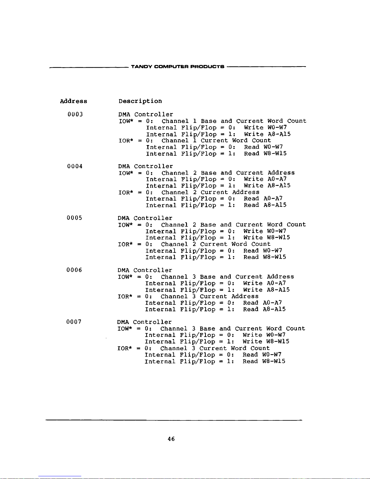
Address
0000
0001
0002
Description
DMA Controller
IOW* = 0: Channel 0 Base and Current Address
Internal Flip/Flop = 0: Write A0-A7
Internal Flip/Flop = 1: Write A8-A15
IOR* = O: Channel 0 Current Address
Internal Flip/Flop = 0: Read A0-A7
Internal Flip/Flop = 1: Read A8-A15
DMA Controller
IOW* = 0: Channel 0 Base and Current Word Count
Internal Flip/Flop = 0: Write W0-W7
Internal Flip/Flop = 1: Write W3-W15
IOR*
= 0:
Channel 0 Current Word Count
Internal Flip/Flop = 0: Read W0-W7
Internal Flip/Flop = 1: Read W8-W15
DMA Controller
IOW* = 0: Channel 1 Base and Current Address
Internal Flip/Flop = 0: Write A0-A7
Internal Flip/Flop = 1: Write A8-A15
IOR* = 0: Channel 1 Current Address
Internal Flip/Flop = 0: Read A0-A7
Internal Flip/Flop = 1: Read A8-A15
.
TANDY COMPUTER PRODUCTS -
Address
0003
0004
0005
0006
0007
Description
DMA Controller
IOW* = 0: Channel 1 Base and Current Word Count
Internal Flip/Flop = 0: Write W0-W7
Internal Flip/Flop = 1: Write A8-A15
IOR* = 0: Channel 1 Current Word Count
Internal Flip/Flop = 0: Read W0-W7
Internal Flip/Flop = 1: Read W8-W15
DMA Controller
IOW* = 0: Channel 2 Base and Current Address
Internal Flip/Flop = 0: Write A0-A7
Internal Flip/Flop = 1: Write A8-A15
IOR* = 0: Channel 2 Current Address
Internal Flip/Flop = 0: Read A0-A7
Internal Flip/Flop = 1: Read A8-A15
DMA Controller
IOW* = 0: Channel 2 Base and Current Word Count
Internal Flip/Flop = 0: Write W0-W7
Internal Flip/Flop = 1: Write W8-W15
IOR* = 0: Channel 2 Current Word Count
Internal Flip/Flop = 0: Read W0-W7
Internal Flip/Flop = 1: Read W8-W15
DMA Controller
IOW* = 0: Channel 3 Base and Current Address
Internal Flip/Flop = 0: Write A0-A7
Internal Flip/Flop = 1: Write A8-A15
IOR* = 0: Channel 3 Current Address
Internal Flip/Flop = 0: Read A0-A7
Internal Flip/Flop = 1: Read A8-A15
DMA Controller
IOW* = 0: Channel 3 Base and Current Word Count
Internal Flip/Flop = 0: Write W0-W7
Internal Flip/Flop = 1: Write W8-W15
IOR* = 0: Channel 3 Current Word Count
Internal Flip/Flop = 0: Read W0-W7
Internal Flip/Flop = 1: Read W8-W15
46

•
TANDY COMPUTER PRODUCTS •
47
0008
Bit
0
1
2
3
4
5
6
7
Bit
0
1
2
3
4
5
6
7
0009
Bit
0-1
2
3-7
DMA Controller
IOW*
= 0,
Write Command Register
Description
0 = Memory
to
Memory Disable
1 = Memory
to
Memory Enable
0 = Channel 0 Address Hold Disable
1 = Channel 0 Address Hold Enable
X
If bit 0=0
0 = Controller enable
1 = Controller disable
0 = Normal timing
1 = Compressed timing
X
If bit 0=1
0 = Fixed priority
1 = Rotating priority
0 = Late write selection
1 = Extended write selection
X
= If bit 3=1
0 = DREQ sense active high
1 = DREQ sense active
low
0 = DACK sense active
low
1 = DACK sense active high
IOR*
= 0,
Read Status Register
Description
1 = Channel
0 has
reached
TC
1 = Channel
1 has
reached
TC
1 = Channel
2 has
reached
TC
1 = Channel
3 has
reached
TC
1 = Channel 0 Request
1 = Channel 1 Request
1 = Channel 2 Request
1 = Channel 3 Request
DMA Controller
IOW*
= 0,
Write Request Register
Description
Bitl BitO
0
0
Select channel
0
0
1
Select channel
1
1
0
Select channel
2
1
1
Select channel
3
0 Reset request
bit
1
Set
request
bit
Don't Care
IOR*
= 0,
Illegal
•
TANDY COMPUTER PRODUCTS •
48
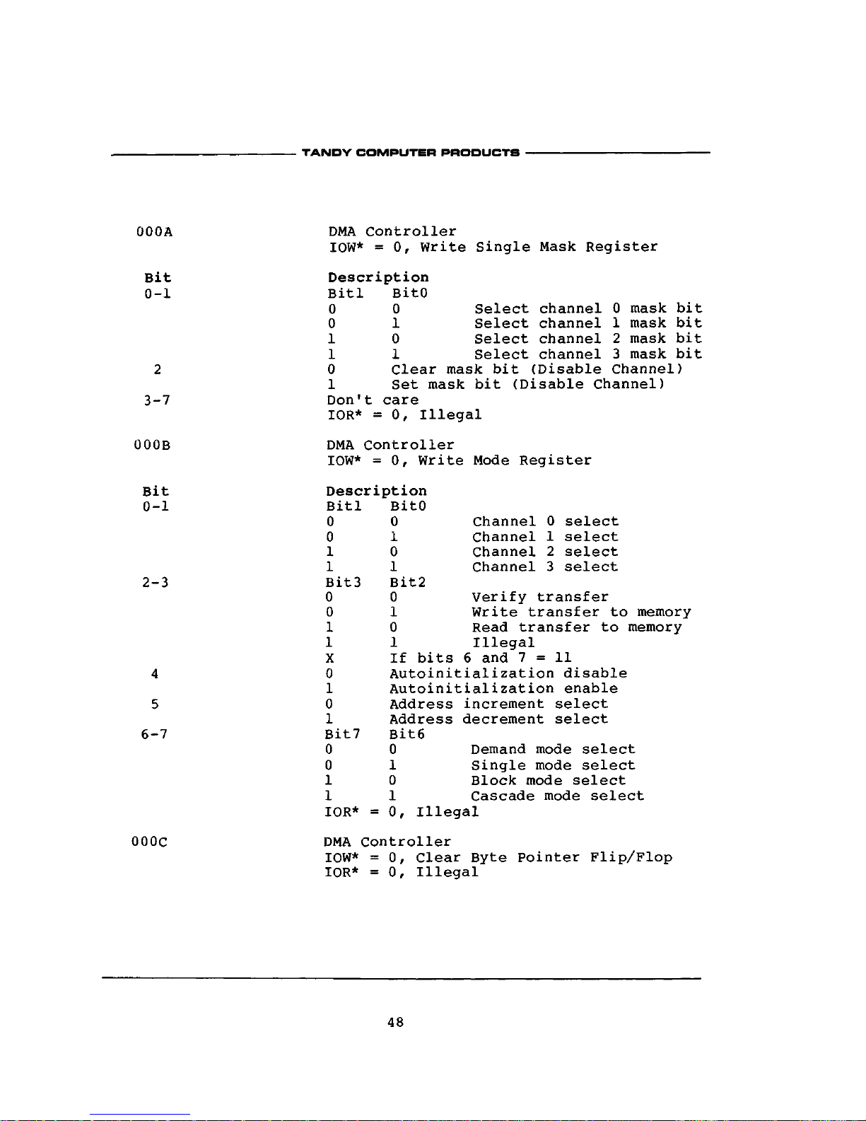
OOOA
Bit
0-1
2
3-7
OOOB
Bit
0-1
2-3
4
5
6-7
oooc
DMA Controller
IOW* = 0f Write Single Mask Register
Description
Bitl BitO
0
0
Select channel 0 mask bit
0
1
Select channel 1 mask bit
1
0
Select channel 2 mask bit
1
1
Select channel 3 mask bit
0 Clear mask bit (Disable Channel)
1 Set mask bit (Disable Channel)
Don't care
IOR* = 0, Illegal
DMA Controller
IOW* = 0f Write Mode Register
Description
Bitl BitO
0
0
Channel 0 select
0
1
Channel 1 select
1
0
Channel 2 select
1
1
Channel 3 select
Bit3 Bit2
0
0
Verify transfer
0
1
Write transfer to memory
1
0
Read transfer to memory
1
1
Illegal
X If bits 6 and 7 = 11
0 Autoinitialization disable
1 Autoinitialization enable
0 Address increment select
1 Address decrement select
Bit7 Bit6
0
0
Demand mode select
0
1
Single mode select
1
0
Block mode select
1
1
Cascade mode select
IOR* = 0, Illegal
DMA Controller
IOW* = 0, Clear Byte Pointer Flip/Flop
IOR* = 0, Illegal
TANDY COMPUTER PRODUCTS •
49
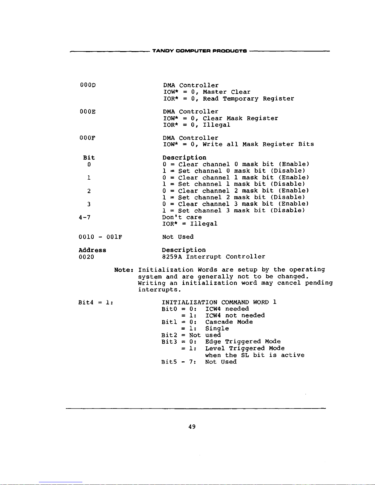
OOOD
OOOE
OOOF
Bit
0
1
2
3
4-7
OO1O - 001F
Address
0020
Note:
Bit4
= 1:
DMA Controller
IOW* = 0, Master Clear
IOR* = 0, Read Temporary Register
DMA Controller
IOW* = 0, Clear Mask Register
IOR* = 0, Illegal
DMA Controller
IOW* = 0, Write all Mask Register Bits
Description
0 = Clear channel 0 mask bit (Enable)
1 = Set channel 0 mask bit (Disable)
0 = Clear channel 1 mask bit (Enable)
1 = Set channel 1 mask bit (Disable)
0 = Clear channel 2 mask bit (Enable)
1 = Set channel 2 mask bit (Disable)
0 = Clear channel 3 mask bit (Enable)
1 = Set channel 3 mask bit (Disable)
Don't care
IOR* = Illegal
Not Used
Description
8259A Interrupt Controller
Initialization Words are setup
by
the operating
system and are generally not
to be
changed.
Writing
an
initialization word may cancel pending
interrupts.
INITIALIZATION COMMAND WORD
1
BitO = 0: ICW4 needed
= 1: ICW4 not needed
Bitl = 0: Cascade Mode
= 1: Single
Bit2 = Not used
Bit3 = 0: Edge Triggered Mode
= 1: Level Triggered Mode
when the
SL
bit
is
active
Bit5 - 7: Not Used

•
TANDY COMPUTER PRODUCTS •
50
Bit4
= 0 &
OPERATION CONTROL WORD
2
Bit3
= 0
BitO - 2:
Determine
the
interrupt level acted
on
when
the
SL
bit
is
active
Interrupt Level =01234567
BitO
(L0):
01010101
Bitl
(Ll):
00110011
Bit2
(L2):
00001111
Bit5
- 7
Control Rotate
and End
of
Interrupt
modes
B7
0
0
1
1
0
1
1
0
B6
0
1
0
0
0
1
1
1
B5
1
1
1
0
0
1
0
0
Non-specific
EOI
command
Specific
EOI
command
Rotate
on
non-specific
EOI
command
Rotate
in
Automatic
EOI
Mode
(set)
Rotate
in
Automatic
EOI
Mode (clear)
*Rotate
on
Specific
EOI
command
*Set priority command
No operation
End
of
Interrupt
End
of
Interest
Automatic Rotation
Automatic Rotation
Automatic Rotation
Specific Rotation
Specific Rotation
*LO
- L2
are
used
Bit4
= 0 &
Bit3
= 1
OPERATION CONTROL WORD
3
BitO
- 1:
Bitl BitO- Read Register Command
0
0 - No
Action
0
1 - No
Action
1
0 -
Read
IR
Register
on
next IOR* Pulse
1
1 -
Read
IS
Register
on
next IOR* Pulse
Bit2 =0:
No
Poll Command
=
1:
Poll Command
Bit5
- 6:
Bit6
Bit5-
Special Mask Mode
0
0 - No
Action
0
1 - No
Action
1
0 -
Reset Special Mask
1
1 -
Set
Special Mask
Bit7
= 0
•
TANDY COMPUTER PRODUCTS
51
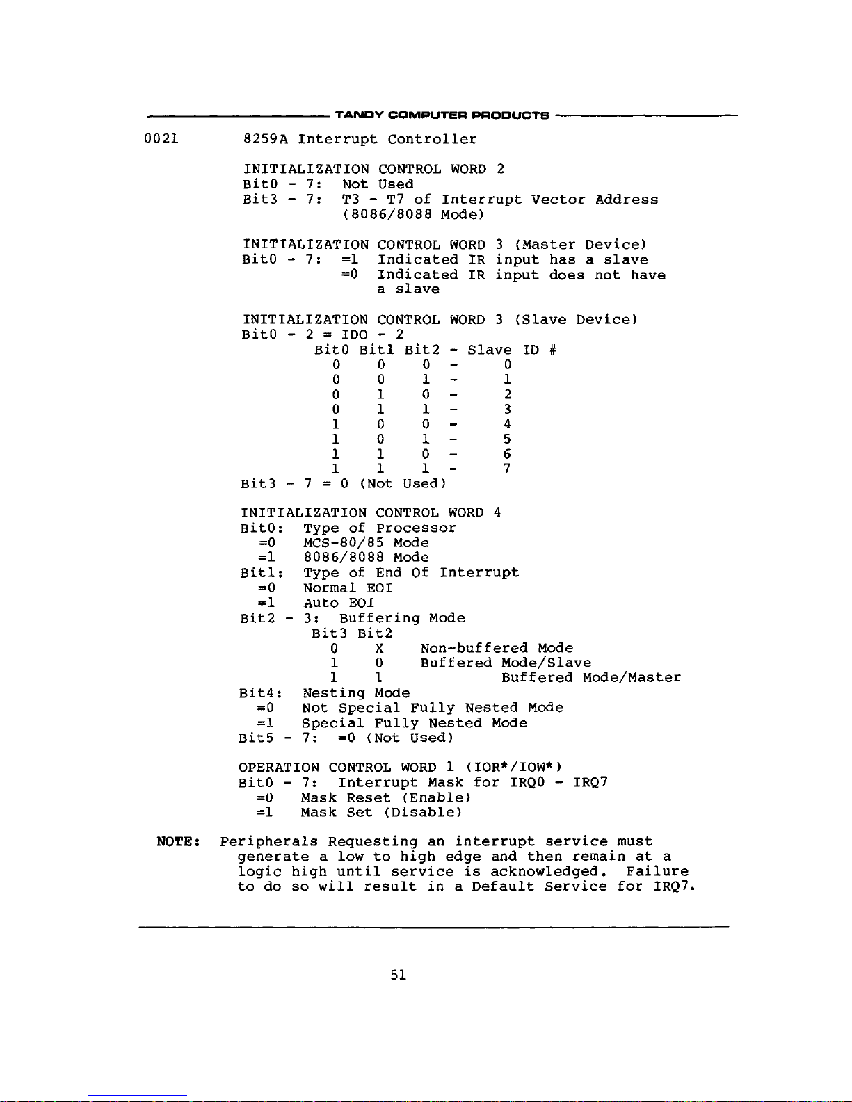
NOTE:
Peripherals Requesting an interrupt service must
generate a low to high edge and then remain at
a
logic high until service is acknowledged. Failure
to do so will result in a Default Service for
IRQ7.
0021 8259A Interrupt Controller
INITIALIZATION CONTROL WORD
2
BitO - 7: Not Used
Bit3 - 7: T3 - T7 of Interrupt Vector Address
(8086/8088 Mode)
INITIALIZATION CONTROL WORD 3 (Master Device)
BitO - 7:
=1
Indicated IR input has a slave
=0 Indicated IR input does not have
a slave
INITIALIZATION CONTROL WORD 3 (Slave Device)
BitO
- 2 =
IDO
- 2
Bit3 -7=0 (Not Used)
INITIALIZATION CONTROL WORD
4
BitO:
Type of Processor
=0 MCS-80/85 Mode
=1 8086/8088 Mode
Bitl:
Type of End Of Interrupt
=0 Normal EOI
=1 Auto EOI
Bit2 - 3: Buffering Mode
Bit3 Bit2
0
X
Non-buffered Mode
1
0
Buffered Mode/Slave
1
1
Buffered Mode/Master
Bit4:
Nesting Mode
=0 Not Special Fully Nested Mode
=1 Special Fully Nested Mode
Bit5 - 7:
=0
(Not Used)
OPERATION CONTROL WORD 1 (IOR*/IOW*)
BitO - 7: Interrupt Mask for IRQ0 - IRQ7
=0 Mask Reset (Enable)
=1 Mask Set (Disable)
BitO
0
0
0
0
1
1
1
1
Bitl
0
0
1
1
0
0
1
1
Bit2
0
1
0
1
0
1
0
1
- Slave ID
#
0
1
2
3
4
5
6
7
TANDY COMPUTER PRODUCTS -
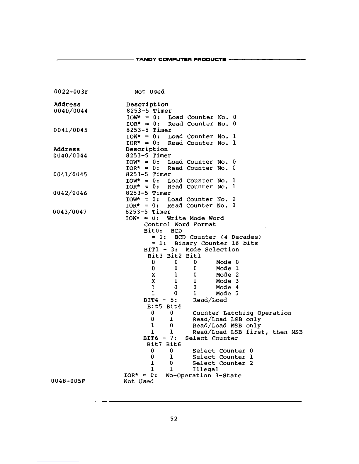
0022-003F
Address
0040/0044
0041/0045
Address
0040/0044
0041/0045
0042/0046
0043/0047
0048-005F
52
Not Used
Description
8253-5 Timer
IOW* = 0: Load Counter No.
0
IOR* = 0: Read Counter No.
0
8253-5 Timer
IOW* = 0: Load Counter No.
1
IOR* = 0: Read Counter No.
1
Description
8253-5 Timer
IOW* = 0: Load Counter No.
0
IOR* = 0: Read Counter No.
0
8253-5 Timer
IOW* = 0: Load Counter No.
1
IOR* = 0: Read Counter No.
1
8253-5 Timer
IOW* = 0: Load Counter No.
2
IOR* = 0: Read Counter No.
2
8253-5 Timer
IOW* = 0: Write Mode Word
Control Word Format
BitO:
BCD
= 0: BCD Counter (4 Decades)
= 1: Binary Counter
16
bits
BIT1 - 3: Mode Selection
Bit3
0
0
X
X
1
1
Bit2
0
0
1
1
0
0
Bitl
0
0
0
1
0
1
Mode
0
Mode
1
Mode
2
Mode
3
Mode
4
Mode
5
BIT4 - 5: Read/Load
Bit5
0
0
1
1
Bit4
0
1
0
1
Counter Latching Operation
Read/Load LSB only
Read/Load MSB only
Read/Load
LSB
first, then
MSB
BIT6 - 7: Select Counter
Bit7
0
0
1
1
Bit6
0
1
0
1
Select Counter
0
Select Counter
1
Select Counter
2
Illegal
IOR* = 0: No-Operation
3-State
Not Used

0060
0061
0062
•
TANDY COMPUTER PRODUCTS •
PORT
A /
KEYBOARD INTERFACE CONTROL PORTS
(READ ONLY)
BIT Description
0 Keyboard
Bit 0-LSB
1 Keyboard
Bit
1
2 Keyboard
Bit
2
3 Keyboard
Bit
3
4 Keyboard
Bit
4
5 Keyboard
Bit
5
6 Keyboard
Bit
6
7 Keyboard
Bit 7-MSB
PORT
B -
READ
or
WRITE
BIT Description
0
1 =
8253 Gate
#2
Enable
1
1 =
Speaker Data
Out
Enable
2
Not
Used
3
Not
Used
4
1 =
Disable Internal Speaker
(Sound Control
2)
5
0 =
Not
Used
6
0 =
Not
Used
7
1 =
Keyboard Clear
PORT
C -
READ/WRITE:
BITS
4-7
Bits
0-3;
READ ONLY:
0063-007F
Address
0080
BIT
0
1
2
3
4
5
6
7
Description
(Output)
Not
Used
(Output)
Not
Used
(Output)
Not
Used
(Output)
CPU
Clock Rate
0 = 4.77 MHz (PC
Compatible Rate)
1 = 7.16 MHz
(Default
by
Boot
ROM)
EEPROM Serial Data Read
8253
Out
#2
Monochrome Mode
0 = Color Monitor
1 = (Not
Supported)
0 = Reserved
Not Used
Description
DMA Page
Reg. (Not
Used)
53

.
TANDY COMPUTER PRODUCTS
54
0081
Address
Bit
Bit
Bit
Bit
Bit
Bit
Bit
Bit
7
0082
0
1
2
3
4
5
6
Address
Bit
Bit
Bit
Bit
Bit
Bit
Bit
Bit
0083
0
1
2
3
4
5
6
7
Address
Bit
Bit
Bit
Bit
Bit
Bit
Bit
Bit
0
1
2
3
4
5
6
7
0084-008F
00A0-00A7
Bit
0
1
2
3
4
5
6
7
WRITE ONLY
Description
DMA
Ch 2
Address
A16
DMA
Ch 2
Address
A17
DMA
Ch 2
Address
A18
DMA
Ch 2
Address
A19
Not Used
Not Used
Not Used
Not Used
WRITE ONLY
Description
DMA
Ch 3
Address
A16
DMA
Ch 3
Address
A17
DMA
Ch 3
Address
Al8
DMA
Ch 3
Address
A19
Not Used
Not Used
Not Used
Not Used
WRITE ONLY
Description
DMA
Ch 0 - 1
Address
A16
DMA
Ch 0 - 1
Address
A17
DMA
Ch 0 - 1
Address
A18
DMA
Ch 0 - 1
Address
A19
Not Used
Not Used
Not Used
Not Used
Not Used
NMI Mask Register, Write only
Description
External Video
0 = Normal Operation
1 = All Video Addresses
and Ports are Disabled
MEMCONFIG
1 -
A17 128K
SW
MEMCONFIG
2 -
A18 256K
SW
MEMCONFIG
3 - A19
512K
SW
"1"
Enable 256K
of
Video
RAM
Not Used
Not Used
1 = Enable
NMI
0 = Disabled

.
TANDY COMPUTER PRODUCTS •
BIT
4
256K
Enable
0
0
0
0
0
1
1
1
1
BIT
3
A19
0
0
0
0
1
0
0
0
1
BIT
2
A18
0
0
1
1
0
0
1
1
0
BIT
1
A17
0
1
0
1
0
1
0
0
0
MEMORY
START
0 0000
2 0000
4 0000
6 0000
8 0000
0 0000
2 0000
4 0000
6 0000
MEMORY
LENGTH
128K
128K
128K
128K
128K
256K
256K
256K
256K
MEMORY
RANGE
0 0000-1 FFFF
2 0000-3 FFFF
4 0000-5 FFFF
6 0000-7 FFFF
8 0000-9 FFFF
0 0000-3 FFFF
2 0000-5 FFFF
4 0000-7 FFFF
6 0000-9 FFFF
NOTE:
To
turn
off
on-board video,
be
sure Port AOHr Data
Bit
0 is
a
"1" AND
Video Array Register 3 (Selected
by
writing
03
into
3DAH) Data
Bit 0 (Write
to
Port 3DEH) must
be =
"0" to
disable
3B8H
and
3BAH.
Address
00C0-00C7
Bit7
=
1
=
0
=
1
=
1
=
0
=
1
=
1
=
0
=
1
=
1
=
1
Bit6
0
X
0
0
X
0
1
X
1
1
1
Bit5
0
FO
0
1
FO
1
0
FO
0
1
1
Bit4
0
Fl
1
0
Fl
1
0
Fl
1
0
1
Bit3
F6
F2
AO
F6
F2
AO
F6
F2
AO
X
AO
Description
Sound SN76496
Bit2
F7
F3
Al
F7
F3
Al
F7
F3
Al
FB
Al
Bitl
F8
F4
A2
F8
F4
A2
F8
F4
A2
NFO
A2
BitO
F9
F5
A3
F9
F5
A3
F9
F5
A3
NFI
A3
Update Tone Frequency
1
Additional Frequency Data
Update Tone Attenuation
1
Update Tone Frequency
2
Additional Frequency Data
Update Tone Attenuation
2
Update Tone Frequency
3
Additional Frequency Data
Update Tone Attenuation
3
Update Noise Control
Update Noise Attenuation
55
00A8 - OOAF
Not
Used
00C8-00DF
00E0-01FF
WRITE (IOW*)
0200 - 0207
0208 - 020F
Not Used
Reserved
Joystick
Clear (Resets Integrator
to
Zero)
Not Used

.
TANDY COMPUTER PRODUCTS
0201 READ
Bit
0
1
2
3
4
5
6
7
Addresses
0370 - 0377
0378
Bit
0
1
2
3
4
5
6
7
0379
Bit
0
1
2
3
4
5
6
7
037A (037E)
Bit
0
1
2
3
4
5
6
7
R = Right Joystick,
L =
Left Joystick
Description
R
- X
Horizontal Position
R
- Y
Vertical Position
L
- X
Horizontal Position
L
- Y
Vertical Position
R Button
#1
(Logic
0 =
Button Depressed)
R Button #2 (Logic
0 =
Button Depressed)
L Button #1 (Logic
0 =
Button Depressed)
L Button #2 (Logic
0 =
Button Depressed)
Printer - Read Status
Description
Not Used
Not Used
Not Used
0 = Error
1 = Printer Select
0 = End
of
Form
0 = Acknowledge
0 = Busy
Printer - Control Latch
Description
0 = Strobe
0 = Auto
FD XT
0 = Initialize
0 = Select Printer
1 = Enable Interrupt
0 = Enable Output Data
Not Used
Not Used
56
Not Used
Printer - Data Latch
Description
Data Bit
0 -
LSB
Data Bit
1 -
Data Bit
2 -
Data Bit
3 -
Data Bit
4 Data Bit
5 Data Bit
6 Data Bit
7 -
MSB

.
TANDY COMPUTER PRODUCTS •
037B
037C
037D - 03D3
03D4
03D5
0 3D6
0 3D7
03D8
Bit
0
Bit
1
Bit
2
Bit
3
Bit
4
Bit
5
03D9
Bit
0
Bit
1
Bit
2
Bit
3
Bit
4
Bit
5
03DA, 03DE
Not Used
DO - Serial Data Write
Dl - EEPROM Chip Enable
D2 - Serial Data Clock
Not Used
6845 Address Register
6845 Data Register
Not Used
Not Used
Mode Select Register
High Resolution Clock
=0:
Selects
40 by 25
Alphanumeric Mode
=1:
Selects
80 by 25
Alphanumeric Mode
Graphics Select
=0:
Selects Alphanumeric Mode
=1:
Selects
320 by
200 Graphics Mode
Black and White
=0:
Selects Color Mode
=1:
Selects Black
and
White Mode
Video Enable
=0:
Disables Video Signal
=1:
Enables Video Signal
640
Dot
Graphics
=0:
Disables
640 by
200
B&W
Graphics Mode
=1:
Enables
640 by
200
B&W
Graphics Mode
Blink Enable
=0:
Disables Blinking
=1:
Enables Blinking
Color Select Register
Background Blue
Background Green
Background
Red
Background Intensity
Foreground Intensity
Color Select
Write Video Array Address & Read Status
(3DA)
Write Video Array Data (3DE)
57

•
TANDY COMPUTER PRODUCTS
READ (3DA)
00 Bit
0
00 Bit
1
00 Bit
2
00 Bit
3
00 Bit
4
01 Bit
0
01 Bit
1
01 Bit
2
01 Bit
3
02 Bit
0
02 Bit
1
02 Bit
2
02 Bit
3
02 Bit
5
03 Bit
0
03 Bit
1
03 Bit
2
03 Bit
3
03 Bit
4
03 Bit
5
10-lF Bit
0
10-lF Bit
1
10-lF Bit
2
10-lF Bit
3
Bits 4-7
03DB
03DC
03DD
Bit
0
1
2
3
4
5
6
7
Display Inactive
Light Pen Set
Light Switch Status
Vertical Retrace
Not Used
WRITE (3DE)
Not Used
Not Used
Not Used
Not Used
Not Used
Palette Mask
0
Palette Mask
1
Palette Mask
2
Palette Mask
3
Border Blue
Border Green
Border Red
Border Intensity
Reserved
= 0
Mono Enable = "1"
Reserved
= 0
Border Enable
4-Color High Resolution
16 Color Mode
Extra Video Mode
Palette Blue
Palette Green
Palette Red
Palette Intensity
Not Used
Clear Light Pen Latch
(Not Used on Tandy 1000 HX)
Preset Light Pen Latch
(Not Used on Tandy 1000 HX)
Extended Ram Page Register - CPU Relative
Description
Extended Addressing Modes
Not Used
Not Used
CRT Video Page Address "17"
CRT Video Page Address "18"
CPU Page Address "17"
CPU Page Address "18"
Select 64K or 256K Ram
58

03DF
Bit
0
Bit
1
Bit
2
Bit
3
Bit
4
Bit
5
Bit
6
Bit
7
03F1
03F2,
3F0, 3F3
03F4,
3F6
03F5f 3F7
03F8 - 03FF
•
TANDY COMPUTER PRODUCTS •
CRT Processor Page Register
- Video Mem Relative
A14 CRT Page
0
A15 CRT Page
1
A16 CRT Page
2
A14 Processor Page
0
A15 Processor Page
1
A16 Processor Page
2
Video Address Mode
0
Video Address Mode
1
DO - Not Used
Dl - = 1 DSO = DSO
= 0 DSO = DS2
D2
- = 1
(3 Drive Selects)
DOR Register (Write Only)
BitO - 1: Drive Select
Bitl BitO
0
0
Drive Select A*
0
1
Drive Select B*
1
0
Drive Select C*
Bit2:
0 =
FDC Reset
Bit3:
1 =
Enable DMA Req/Interrupt
Bit4:
1 =
Drive A Motor On
Bit5:
1 =
Drive B Motor On
Bit6:
1 =
FDC Terminal Count
Bit7:
Not Used
FDC - Status (Read Only)
- See FDC Specification
FDC - Data (R/W) - See FDC Specification
COM 1 Port
For Ports 3F0 - 3F7, the following general conditions apply:
Al = Don't Care
For DOR, A2
= 0
For FDC, A2
= 1
59
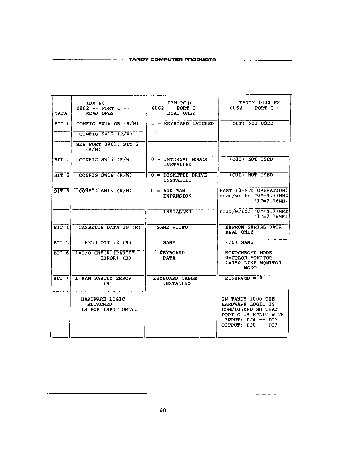
TANDY COMPUTER PRODUC
60
DATA
BIT
0
BIT
1
BIT
2
BIT
3
BIT
4
BIT
5
BIT
6
BIT
7
IBM
PC
0062 — PORT
C —
READ ONLY
CONFIG SW16
OR
(R/W)
CONFIG SW12 (R/W)
SEE PORT 0061,
BIT 2
(R/W)
CONFIG SW15 (R/W)
CONFIG SW14
(R/W)
CONFIG SW13
(R/W)
CASSETTE DATA
IN (R)
8253
OUT #2 (R)
1=1/0 CHECK (PARITY
ERROR)
(R)
1=RAM PARITY ERROR
(R)
HARDWARE LOGIC
ATTACHED
IS
FOR
INPUT ONLY.
IBM PCjr
0062 — PORT
C —
READ ONLY
1 = KEYBOARD LATCHED
0 = INTERNAL MODEM
INSTALLED
0 = DISKETTE DRIVE
INSTALLED
0 = 64K RAM
EXPANSION
INSTALLED
SAME VIDEO
SAME
KEYBOARD
DATA
KEYBOARD CABLE
INSTALLED
TANDY 1000
HX
0062 — PORT
C —
(OUT) NOT USED
(OUT) NOT USED
(OUT) NOT USED
FAST (0=STD OPERATION)
read/write
ll
0"=4 .77MHz
"1"=7.16MHz
read/write "0"=4.77MHz
"1"=7.16MHz
EEPROM SERIAL DATAREAD ONLY
(IN) SAME
MONOCHROME MODE
0=COLOR MONITOR
1=350 LINE MONITOR
MONO
RESERVED
= 0
IN TANDY 1000
THE
HARDWARE LOGIC
IS
CONFIGURED
SO
THAT
PORT
C IS
SPLIT WITH
INPUT:
PC4
— PC7
OUTPUT:
PC0
— PC3

•
TANDY COMPUTER PRODUCTS •
DATA
BIT
0
BIT
1
BIT
2
\
1
BIT
3
BIT
4
BIT
5
BIT
6
Br
\
1
7
r
IBM
PC
0061 — PORT
B —
READ
OR
WRITE
1=8253 GATE
#2 ENABLED
SPEAKER DATA
OUT
1=ENABLE READING
CONFIG SW13 THRU
16
(I/O CHAN
ROM
SIZE)
OR
0=ENABLE READING
CONFIG SW12 (@PC0
—
PC3)
1=CASSETTE MOTOR
OFF
0=ENABLE
RAM
PARITY
0=ENABLE
I/O CH
PARITY
0=HOLD KEYBOARD
CLK
LOW
0=ENABLE KEYBOARD
1=CLEAR KEYBOARD
AND
ENABLE CONFIG
SW 1-8
IBM PCjr
0061 — PORT
B —
READ
OR
WRITE
SAME
SAME
1=ALPHA (GRAPHICS)
SAME
1=DISABLE CASSETTE
MTR
RELAY,
INTERNAL BEEPER
SPKR
SW 0
SPKR
SW 1
1=KEYBOARD CLEAR
TANDY 1000
HX
0061 — PORT
B —
READ
OR
WRITE
SAME
SAME
NO FUNCTION
NO FUNCTION
1=DISABLE INTERNAL
SPEAKER (SOUNDCONT2)
1=KEYBOARD CLEAR
61

•
TANDY COMPUTER PRODUCTS
VIDEO / SYSTEM MEMORY ADDRESS
MAP
OAO
BIT
4
0*
0
0
0
0
1
1
1
1
MC3
OAO
BIT
3
A19
0
0
0
0
1
0
0
0
1
MC2
OAO
BIT
2
A18
0
0
1
1
0
0
1
1
0
MCl
OAO
BIT
1
A17
0
1
0
1
0
1
0
1
0
VIDEO/SYSTEM
MEMORY
START
ADDRESS
00000
(0)
20000
(128K)
40000
(256K)
60000
(324K)
80000
(512K)
00000
(0)
20000
(128K)
40000
(156K)
60000
(384K)
VIDEO/SYSTEM
MEMORY
LENGTH
128K
128K
128K
128K
128K
256K
256K
256K
256K
VIDEO/SYSTEM
MEMORY
ADDRESS
RANGE
00000-1FFFF
20000-3FFFF
40000-5FFFF
60000-7FFFF
80000-9FFFF
00000-3FFFF
20000-5FFFF
40000-7FFFF
60000-9FFFF
*
ENDBIP 256K
OF
VIDEO
ROM IF "1"
62

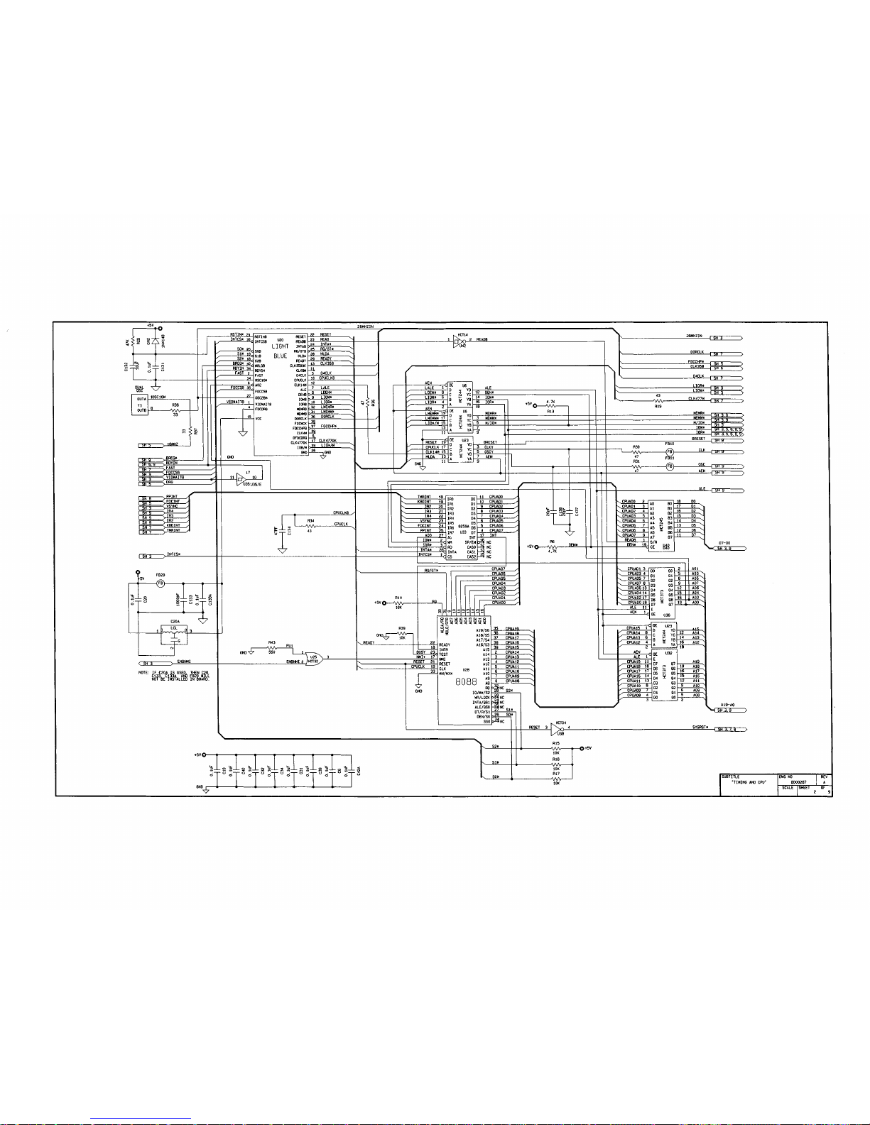


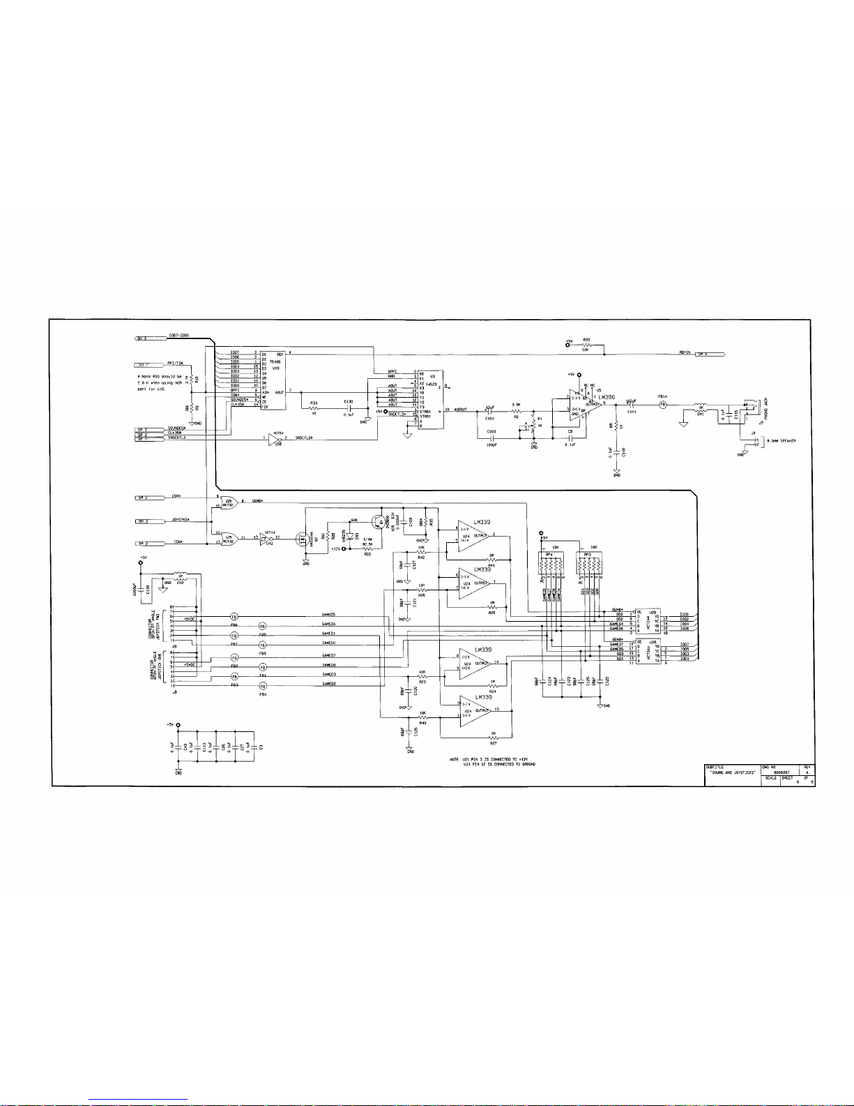


.
TANDY COMPUTER PRODUCTS
1000
HX
Devices

•
TANDY COMPUTER PRODUCTS
1000
HX
Devices
Contents
Device Manufacturer
8088 (CPU) intel
8253 Interval Timer intel
8259A Interrupt Controller intel
Floppy Disk Support Motorola
Keyboard Interface Motorola
8048
NEC
HPD765 (FDC)
NEC
Direct Memory Access (DMA) Tandy
Printer Interface Tandy
Timing Control Generator Tandy
Video Controller Tandy
8496 Sound Generator
NCR
Note:
All Intel Chip Specifications are reprinted
by
permission
of Intel Corporation, Copyright 1987.
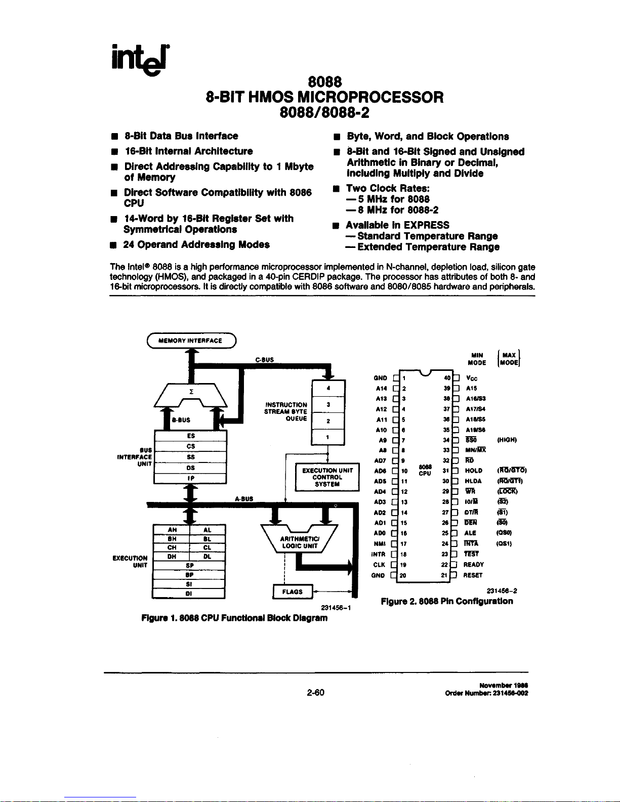
8088
8-BIT
HMOS MICROPROCESSOR
8088/8088-2
8-Bit
Data Bus Interface
16-Bit Internal Architecture
Direct Addressing Capability to 1 Mbyte
of Memory
Direct Software Compatibility with 8086
CPU
14-Word by 16-Bit Register Set with
Symmetrical Operations
24 Operand Addressing Modes
Byte,
Word, and Block Operations
8-Bit
and 16-Bit Signed and Unsigned
Arithmetic in Binary or Decimal,
Including Multiply and Divide
Two Clock Rates:
— 5 MHz for 8088
— 8 MHz for 8088-2
Available in EXPRESS
— Standard Temperature Range
— Extended Temperature Range
The Intel® 8088 is a high performance microprocessor implemented in N-channel, depletion
load,
silicon gate
technology (HMOS), and packaged in a 40-pin CERDIP package. The processor has attributes of both 8- and
16-bit microprocessors. It is directly compatible with 8086 software and 8080/8085 hardware and peripherals.
2-60
Order
Number 231456-002

8088
Table
1.
Pin Description
The
following pin function descriptions are for 8088 systems in either
minimum
or
maximum
mode.
The "local
bus" in these descriptions is the direct multiplexed bus interface connection to the 8088 (without regard to
additional bus buffers).
Symbol
AD7-AD0
A15-A8
A19/S6.A18/S5
A17/S4.A16/S3
m
READY
INTR
TEST
Pin
No
9-16
2-8,
39
35-38
32
22
18
23
Type
I/O
0
0
0
I
I
I
Name and Function
ADDRESS DATA
BUS:
These lines constitute the time multiplexed
memory/IO address (T1) and data
(T2,
T3, Tw, T4)
bus.
These lines are
active HIGH and float to
3-state
OFF during interrupt acknowledge and
local bus "hold acknowledge".
ADDRESS
BUS:
These lines provide address bits 8 through 15 for the
entire bus cycle (T1-T4). These lines do not have to be latched by ALE
to remain
valid.
A15-A8 are active HIGH and float to
3-state
OFF
during interrupt acknowledge and local bus "hold acknowledge".
ADDRESS/STATUS: During
T1,
these are the four most significant
address lines for memory operations. During I/O operations, these lines
are LOW. During memory and I/O operations, status information is
available on these lines during
T2,
T3, Tw, and
T4.
S6 is always low.
The status of the interrupt enable flag bit (S5) is updated at the
beginning of each clock
cycle.
S4 and S3 are encoded as shown.
This information indicates which segment register is presently being
used for data accessing.
These lines float to
3-state
OFF during local bus "hold acknowledge".
S4
0(LOW)
0
1 (HIGH)
1
S6isO(LOW)
S3
0
1
0
1
Characteristics
Alternate Data
Stack
Code or None
Data
READ:
Read strobe indicates that the processor is performing a
memory or I/O read
cycle,
depending on the state of the IO/M pin or
S2.
This signal is used to read devices which reside on the 8088 local
bus.
RU is active LOW during
T2,
T3 and Tw of any read cycle, and is
guaranteed to remain HIGH in T2 until the 8088 local bus has floated.
This signal floats to
3-state
OFF in "hold acknowledge".
READY: is the acknowledgement from the addressed memory or I/O
device that it will complete the data transfer. The RDY signal from
memory or I/O is synchronized by the 8284 clock generator to form
READY. This signal is active
HIGH.
The 8088 READY input is not
synchronized. Correct operation is not guaranteed if the set up and hold
times are not met.
INTERRUPT REQUEST: is a level triggered input which is sampled
during the last clock cycle of each instruction to determine if the
processor should enter into an interrupt acknowledge operation. A
subroutine is vectored to via an interrupt vector lookup table located in
system memory. It can be internally masked by software resetting the
nterrupt enable bit. INTR is internally synchronized. This signal is active
HIGH.
TE§T: input is examined by the "wait for test" instruction. If the TEST
nput is LOW, execution continues, otherwise the processor waits in an
'idle"
state. This input is synchronized internally during each clock
cycle on the leading edge of CLK.
2-61
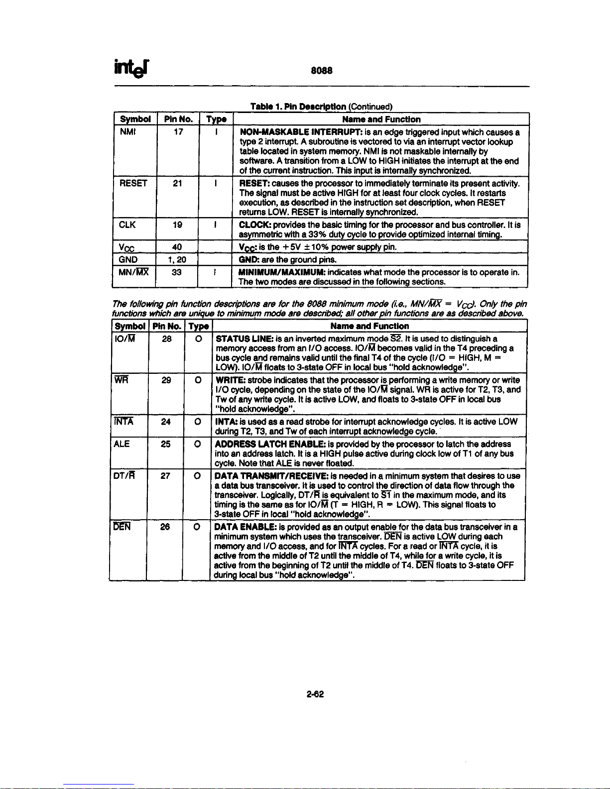
8088
Table
1.
Pin Description (Continued)
Symbol
NMI
RESET
CLK
Vcc
GND
MN/MX
Pin
No.
17
21
19
40
1,20
33
Type
I
I
I
I
Name and Function
NON-MASKABLE INTERRUPT: is an edge triggered input which causes a
type 2 interrupt. A subroutine is vectored to via an interrupt vector lookup
table located in system memory. NMI is not maskable internally by
software. A transition from a LOW to HIGH initiates the interrupt at the end
of the current
instruction.
This input is internally synchronized.
RESET: causes the processor to immediately terminate its present activity.
The signal must be active HIGH for at least four clock cycles. It restarts
execution,
as described in the instruction set
description,
when RESET
returns LOW. RESET is internally synchronized.
CLOCK: provides the basic timing for the processor and bus controller. It is
asymmetric with a
33%
duty cycle to provide optimized internal timing.
VCc-" js the + 5V ±10% power supply pin.
QND:
are the ground pins.
MINIMUM/MAXIMUM: indicates what mode the processor is to operate in.
The two modes are discussed in the following sections.
The following pin function descriptions are for the 8088 minimum mode
(i.e.,
MN/MX = Vcc)- Only the pin
functions which are unique to minimum mode are
described;
all other pin functions are as described
above.
Symbol
lO/Ef
WR
IF3TA
ALE
DT/E
Pin
No.
28
29
24
25
27
26
Type
o
0
0
0
0
0
Name and Function
STATUS
LINE:
is an inverted maximum mode
§2.
It is used to distinguish a
memory access from an I/O access. IO/M becomes valid in the T4 preceding a
bus cycle and remains valid until the final T4 of the cycle (I/O = HIGH, M =
LOW). IO/M floats to
3-state
OFF in local bus "hold acknowledge".
WRITE:
strobe indicates that the processor is performing a write memory or write
I/O
cycle,
depending on the state of the IO/M signal. WR is active for
T2,
T3, and
Tw of any write cycle. It is active LOW, and floats to
3-state
OFF in local bus
"hold acknowledge".
INTA: is used as a read strobe for interrupt acknowledge cycles. It is active LOW
during
T2,
T3, and Tw of each interrupt acknowledge cycle.
ADDRESS LATCH
ENABLE:
is provided by the processor to latch the address
into an address
latch.
It is a HIGH pulse active during clock low of
T1
of any bus
cycle.
Note that ALE is never floated.
DATA TRANSMIT/RECEIVE: is needed in a minimum system that desires to use
a data bus transceiver. It is used to control the direction of data flow through the
transceiver. Logically, DT/ft is equivalent to ST in the maximum mode, and its
timing is the same as for IO/M (T = HIGH, R = LOW). This signal floats to
3-state
OFF in local "hold acknowledge".
DATA ENABLE: is provided as an output enable for the data bus transceiver in a
minimum system which uses the transceiver. DEN is active LOW during each
memory and I/O access, and for INTA cycles. For a read or INTA cycle, it is
active from the middle of T2 until the middle of
T4,
while for a write cycle, it is
active from the beginning of T2 until the middle of
T4.
DEN floats to
3-state
OFF
during local bus "hold acknowledge".
2-62
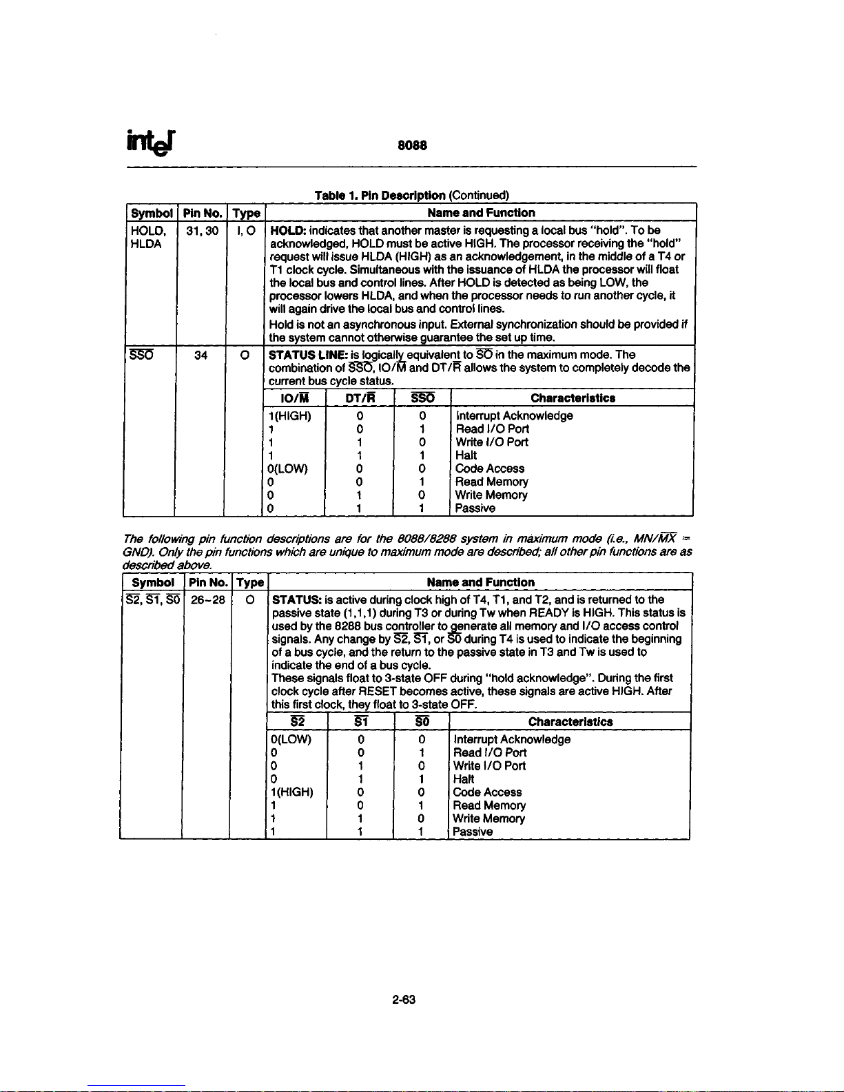
8088
Table 1. Pin Description (Continued)
Symbol
HOLD,
HLDA
SSC5
Pin No.
31,30
34
Type
l,0
0
Name and Function
HOLD:
indicates that another master is requesting a local bus
"hold".
To be
acknowledged, HOLD must be active
HIGH.
The processor receiving the
"hold"
request will issue HLDA (HIGH) as an acknowledgement, in the middle of a T4 or
T1 clock
cycle.
Simultaneous with the issuance of HLDA the processor will float
the local bus and control lines. After HOLD is detected as being LOW, the
processor lowers HLDA, and when the processor needs to run another
cycle,
it
will again drive the local bus and control lines.
Hold is not an asynchronous input. External synchronization should be provided if
the system cannot otherwise guarantee the set up time.
STATUS
LINE:
is logical ^equivalent to SO in the maximum mode. The
combination of
SSO,
IO/M and DT/R allows the system to completely decode the
current bus cycle status.
IO/M
KHIGH)
1
1
1
0(LOW)
0
0
0
DT/R
0
0
1
1
0
0
1
1
SSO
0
1
0
1
0
1
0
1
Characteristics
Interrupt Acknowledge
Read I/O Port
Write I/O Port
Halt
Code Access
Read Memory
Write Memory
Passive
The following pin function descriptions are for the 8088/8288 system in maximum mode (i.e., MN/MX =
GND).
Only
the
pin functions
which
are unique to
maximum
mode are
described;
all other pin functions are as
described
above.
Symbol
S2.ST.S0
Pin
No.
26-28
Type
0
Name and Function
STATUS: is active during clock high of
T4,
T1,
and
T2,
and is returned to the
passive state (1,1,1) during T3 or during Tw when READY is
HIGH.
This status is
used by the 8288 bus controller to_generate all memory and I/O access control
signals. Any change by
S2,
S1,
or
SO
during T4 is used to indicate the beginning
of a bus
cycle,
and the return to the passive state in T3 and Tw is used to
indicate the end of a bus cycle.
These signals float to
3-state
OFF during "hold acknowledge". During the first
clock cycle after RESET becomes
active,
these signals are active
HIGH.
After
this first clock, they float to
3-state
OFF.
S2
0(LOW)
0
0
0
1(HIGH)
1
1
1
SI
0
0
1
1
0
0
1
1
so
0
1
0
1
0
1
0
1
Characteristics
Interrupt Acknowledge
Read I/O Port
Write I/O Port
Halt
Code Access
Read Memory
Write Memory
Passive
2-63

8088
Table
1.
Pin Description (Continued)
Symbol
RQ/GTO,
Ra/GTT
LOCK
QS1.QS0
Pin
No.
30,31
29
24,25
34
Type
I/O
0
0
0
Name and Function
REQUEST/GRANT: pins are used by other local bus masters to force the
processor to release the local bus at the end of the processor's current bus
cycle.
Eachpn is bidirectional with RQ/CfTO having higher priority than RG/
GT1.
R5/GT has an internal pull-up resistor, so may be left unconnected.
The request/grant sequence is as follows (See Figure 8):
1.
A pulse of one CLK wide from another local bus master indicates a local
bus request
("hold")
to the 8088 (pulse 1).
2.
During a T4 or Tl clock cycle, a pulse one clock wide from the 8088 to the
requesting master (pulse
2),
indicates that the 8088 has allowed the local
bus to float and that it will enter the "hold acknowledge" state at the next
CLK. The CPU's bus interface unit is disconnected logically from the local
bus during "hold acknowledge". The same rules as for HOLD/HOLDA apply
as for when the bus is released.
3. A pulse one CLK wide from the requesting master indicates to the 8088
(pulse 3) that the
"hold"
request is about to end and that the 8088 can
reclaim the local bus at the next CLK. The CPU then enters T4.
Each master-master exchange of the local bus is a sequence of three
pulses. There must be one idle CLK cycle after each bus exchange. Pulses
are active LOW.
If the request is made while the CPU is performing a memory
cycle,
it will
release the local bus during T4 of the cycle when all the following conditions
are
met:
1.
Request occurs on or before T2.
2.
Current cycle is not the low bit of a word.
3. Current cycle is not the first acknowledge of an interrupt acknowledge
sequence.
4.
A locked instruction is not currently executing.
If the local bus is idle when the request is made the two possible events will
follow:
1.
Local bus will be released during the next clock.
2.
A memory cycle will start within 3 clocks. Now the four rules for a currently
active memory cycle apply with condition number 1 already satisfied.
LOCK: indicates that other system bus masters are not to gain control of the
system bus while LOCK is active (LOW). The LOCK signal is activated by
the "LOCK" prefix instruction and remains active until the completion of the
next instruction. This signal is active LOW, and floats to
3-state
off in "hold
acknowledge".
QUEUE
STATUS:
provide status to allow external tracking of the internal
8088 instruction queue.
The queue status is valid during the CLK cycle after which the queue
operation is performed.
QS1
0(LOW)
0
1(HIGH)
1
QS0
0
1
0
1
Characteristics
No Operation
First Byte of Opcode from Queue
Empty the Queue
Subsequent Byte from Queue
3
in 34 is always high in the maximum mode.
2-64
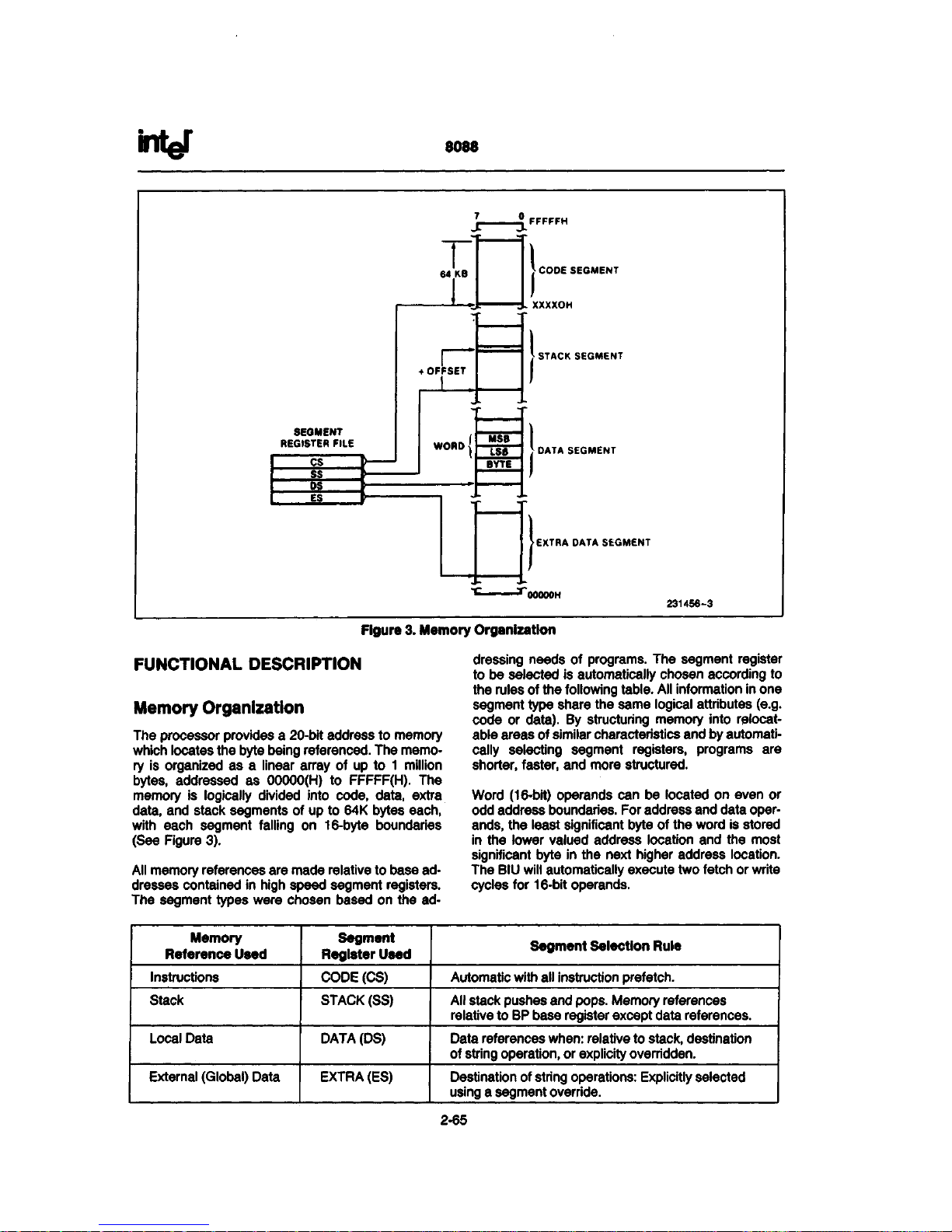
8088
Figure 3. Memory Organization
FUNCTIONAL DESCRIPTION
Memory Organization
The processor provides a 20-bit address to memory
which locates the byte being referenced. The memo-
ry is organized as a linear array of up to 1 million
bytes,
addressed as 00000(H) to FFFFF(H). The
memory is logically divided into code, data, extra
data,
and stack segments of up to 64K bytes each,
with each segment falling on 16-byte boundaries
(See Figure 3).
All memory references are made relative to base addresses contained in high speed segment registers.
The segment types were chosen based on the ad-
dressing needs of programs. The segment register
to be selected is automatically chosen according to
the rules of the following table. All information in one
segment type share the same logical attributes (e.g.
code or data). By structuring memory into relocat-
able areas of similar characteristics and by automati-
cally selecting segment registers, programs are
shorter, faster, and more structured.
Word (16-bit) operands can be located on even or
odd address boundaries. For address and data operands,
the least significant byte of the word is stored
in the lower valued address location and the most
significant byte in the next higher address location.
The BIU will automatically execute two fetch or write
cycles for 16-bit operands.
Memory
Reference Used
Instructions
Stack
Local Data
External (Global) Data
Segment
Register Used
CODE (CS)
STACK (SS)
DATA (DS)
EXTRA (ES)
Segment Selection Rule
Automatic with all instruction prefetch.
All stack pushes and pops. Memory references
relative to BP base register except data references.
Data references
when:
relative to stack, destination
of string operation, or explicity overridden.
Destination of string operations: Explicitly selected
using a segment override.
2-65
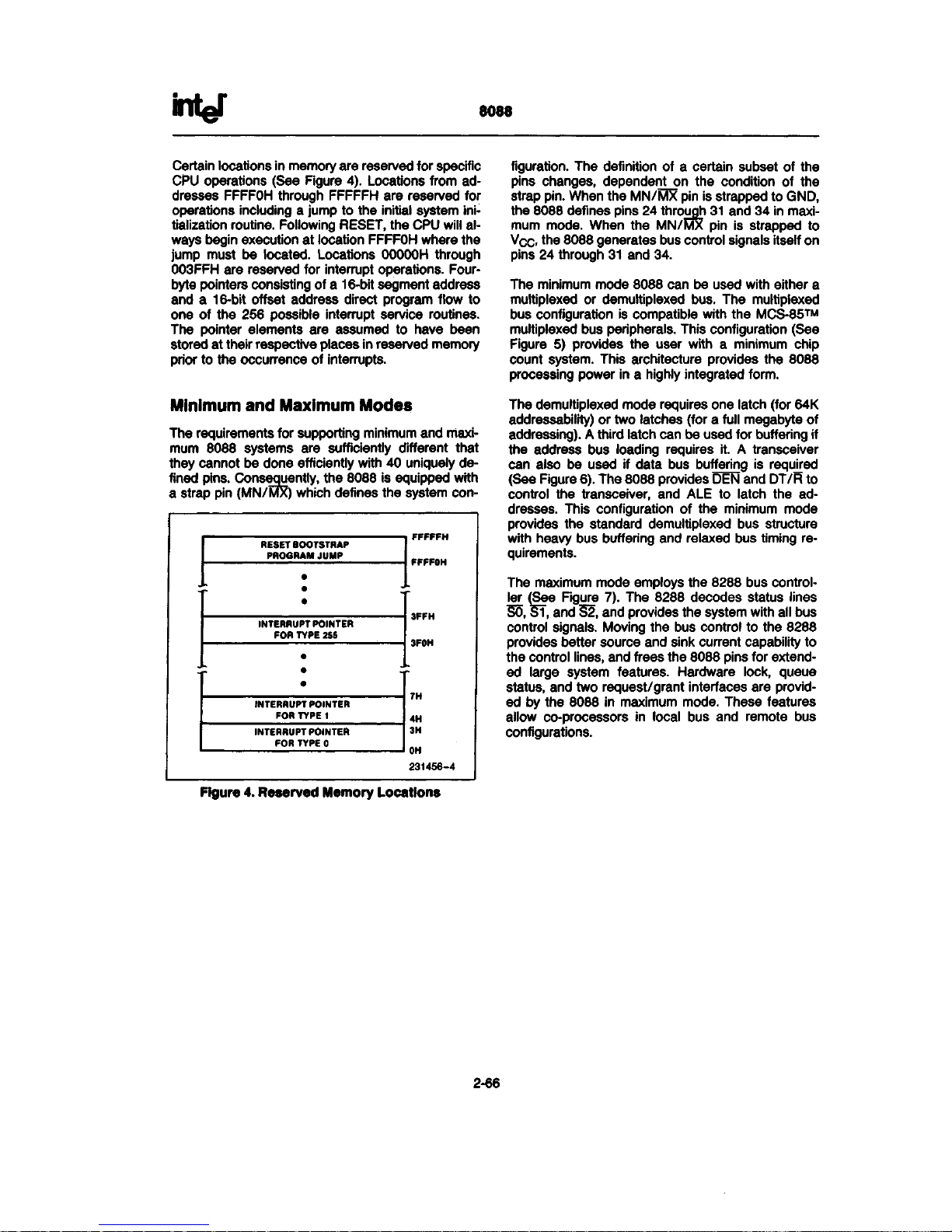
8088
Certain locations in memory are reserved for specific
CPU operations (See Figure 4). Locations from addresses FFFFOH through FFFFFH are reserved for
operations including a jump to the initial system initialization routine. Following RESET, the CPU will always begin execution at location FFFFOH where the
jump must be located. Locations 00000H through
003FFH are reserved for interrupt operations. Four-
byte pointers consisting of a 16-bit segment address
and a 16-bit offset address direct program flow to
one of the 256 possible interrupt service routines.
The pointer elements are assumed to have been
stored at their respective places in reserved memory
prior to the occurrence of interrupts.
Minimum and Maximum Modes
The requirements for supporting minimum and maxi-
mum 8088 systems are sufficiently different that
they cannot be done efficiently with 40 uniquely defined pins. Consequently, the 8088 is equipped with
a strap pin (MN/MX) which defines the system con-
figuration.
The definition of a certain subset of the
pins changes, dependent on the condition of the
strap pin. When the MN/MX pin is strapped to GND,
the 8088 defines pins 24 through
31
and 34 in maximum mode. When the MN/MX pin is strapped to
Vcc- the 8088 generates bus control signals itself on
pins 24 through 31 and 34.
The minimum mode 8088 can be used with either a
multiplexed or demultiplexed bus. The multiplexed
bus configuration is compatible with the MCS-85TM
multiplexed bus peripherals. This configuration (See
Figure 5) provides the user with a minimum chip
count system. This architecture provides the 8088
processing power in a highly integrated form.
The demultiplexed mode requires one latch (for 64K
addressability) or two latches (for a full megabyte of
addressing). A third latch can be used for buffering if
the address bus loading requires it. A transceiver
can also be used if data bus buffering is required
(See Figure
6).
The 8088 provides DEN and DT/R to
control the transceiver, and ALE to latch the addresses. This configuration of the minimum mode
provides the standard demultiplexed bus structure
with heavy bus buffering and relaxed bus timing requirements.
The maximum mode employs the 8288 bus controller (See Figure 7). The 8288 decodes status lines
SO,
5T, and S2, and provides the system with all bus
control signals. Moving the bus control to the 8288
provides better source and sink current capability to
the control lines, and frees the 8088 pins for extended large system features. Hardware lock, queue
status, and two request/grant interfaces are provided by the 8088 in maximum mode. These features
allow co-processors in local bus and remote bus
configurations.
Figure 4. Reserved Memory Locations
2-66

8088
Figure 5. Multiplexed Bus Configuration
2-67

8088
Figure 6. Demultiplexed Bus Configuration
Figure 7. Fully Buffered System Using Bus Controller
2-68

8088
Bus
Operation
The 8088 address/data bus is broken into three
parts—the lower eight address/data bits (ADOAD?),
the middle eight address bits (A8-A15), and
the upper four address bits (A16-A19). The address/data bits and the highest four address bits are
time multiplexed. This technique provides the most
efficient use of pins on the processor, permitting the
use of a standard 40 lead package. The middle eight
address bits are not multiplexed, i.e. they remain val-
id throughout each bus cycle. In addition, the bus
can be demultiplexed at the processor with a single
address latch if a standard, non-multiplexed bus is
desired for the system.
Each processor bus cycle consists of at least four
CLK cycles. These are referred to as
T1,
T2, T3, and
T4 (See Figure 8). The address is emitted from the
processor during T1 and data transfer occurs on the
bus during T3 and T4. T2 is used primarily for chang-
Figure 8. Baste System Timing
2-69

8088
ing the direction of the bus during read operations. In
the event that a "NOT READY" indication is given
by the addressed device, "wait" states (Tw) are inserted between T3 and T4. Each inserted "wait"
state is of the same duration as a CLK cycle. Periods
can occur between 8088 driven bus cycles. These
are referred to as "idle" states (Ti), or inactive CLK
cycles. The processor uses these cycles for internal
housekeeping.
During T1 of any bus cycle, the ALE (address latch
enable) signal is emitted (by either the processor or
the 8288 bus controller, depending on the MN/MX
strap). At the trailing edge of this pulse, a valid address and certain status information for the cycle
may be latched.
Status bits §6, 5T, and S2 are used by the bus controller, in maximum mode, to identify the type of bus
transaction according to the following table:
S2
0(LOW)
0
0
0
1(HIGH)
1
1
1
SI
0
0
1
1
0
0
1
1
so
0
1
0
1
0
1
0
1
Characteristics
Interrupt Acknowledge
Read I/O
Write I/O
Halt
Instruction Fetch
Read Data from Memory
Write Data to Memory
Passive (No Bus Cycle)
Status bits S3 through S6 are multiplexed with high
order address bits and are therefore valid during 12
through T4. S3 and S4 indicate which segment register was used for this bus cycle in forming the address according to the following table:
s
4
0(LOW)
0
1(HIGH)
1
S
3
0
1
0
1
Characteristics
Alternate Data (Extra Segment)
Stack
Code or None
Data
S5 is a reflection of the PSW interrupt enable bit. S6
is always equal to 0.
I/O Addressing
In the 8088, I/O operations can address up to a
maximum of 64K I/O registers. The I/O address appears in the same format as the memory address on
bus lines A15-A0. The address lines A19-A16 are
zero in I/O operations. The variable I/O instructions,
which use register DX as a pointer, have full address
capability, while the direct I/O instructions directly
address one or two of the 256 I/O byte locations in
page 0 of the I/O address space. I/O ports are addressed in the same manner as memory locations.
Designers familiar with the 8085 or upgrading an
8085 design should note that the 8085 addresses
I/O with an
8-bit
address on both halves of the 16bit address bus. The 8088 uses a full 16-bit address
on its lower 16 address lines.
EXTERNAL INTERFACE
Processor Reset and Initialization
Processor initialization or start up is accomplished
with activation (HIGH) of the RESET pin. The 8088
RESET is required to be HIGH for greater than four
clock cycles. The 8088 will terminate operations on
the high-going edge of RESET and will remain dor-
mant as long as RESET is HIGH. The low-going
transition of RESET triggers an internal reset sequence for approximately 7 clock cycles. After this
interval the 8088 operates normally, beginning with
the instruction in absolute locations FFFF0H (See
Figure 4). The RESET input is internally synchronized to the processor clock. At initialization, the HIGH
to LOW transition of RESET must occur no sooner
than 50 jus after power up, to allow complete initiali-
zation of the 8088.
NMI asserted prior to the 2nd clock after the end of
RESET will not be honored. If NMI is asserted after
that point and during the internal reset sequence,
the processor may execute one instruction before
responding to the interrupt. A hold request active
immediately after RESET will be honored before the
first instruction fetch.
All 3-state outputs float to 3-state OFF during
RESET. Status is active in the idle state for the first
clock after RESET becomes active and then floats
to 3-state OFF. ALE and HLDA are driven low.
Interrupt Operations
Interrupt operations fall into two classes: software or
hardware initiated. The software initiated interrupts
and software aspects of hardware interrupts are
specified in the instruction set description in the
iAPX 88 book or the iAPX 86,88 User's Manual.
Hardware interrupts can be classified as nonmaska-
ble or maskable.
2-70

8088
Interrupts result in a transfer of control to a new program location. A 256 element table containing address pointers to the interrupt service program locations resides in absolute locations 0 through 3FFH
(See Figure 4), which are reserved for this purpose.
Each element in the table is 4 bytes in size and corresponds to an interrupt "type." An interrupting de-
vice supplies an 8-bit type number, during the interrupt acknowledge sequence, which is used to vector
through the appropriate element to the new interrupt
service program location.
Non-Maskable Interrupt (NMI)
The processor provides a single non-maskable interrupt (NMI) pin which has higher priority than the
maskable interrupt request (INTR) pin. A typical use
would be to activate a power failure routine. The
NMI is edge-triggered on a LOW to HIGH transition.
The activation of this pin causes a type 2 interrupt.
NMI is required to have a duration in the HIGH state
of greater than two clock cycles, but is not required
to be synchronized to the clock. Any higher going
transition of NMI is latched on-chip and will be serviced at the end of the current instruction or between
whole moves (2 bytes in the case of word moves) of
a block type instruction. Worst case response to
NMI would be for multiply, divide, and variable shift
instructions. There is no specification on the occurrence of the low-going edge; it may occur before,
during,
or after the servicing of NMI. Another highgoing edge triggers another response if it occurs after the start of the NMI procedure. The signal must
be free of logical spikes in general and be free of
bounces on the low-going edge to avoid triggering
extraneous responses.
enable bit will be zero unless specifically set by an
instruction.
During the response sequence (See Figure 9), the
processor executes two successive (back to back)
interrupt acknowledge cycles. The 8088 emits the
LOCK signal (maximum mode only) from T2 of the
first bus cycle until T2 of the second. A local bus
"hold"
request will not be honored until the end of
the second bus cycle. In the second bus cycle, a
byte is fetched from the external interrupt system
(e.g.,
8259A PIC) which identifies the source (type)
of the interrupt. This byte is multiplied by four and
used as a pointer into the interrupt vector lookup
table.
An INTR signal left HIGH will be continually
responded to within the limitations of the enable bit
and sample period. The interrupt return instruction
includes a flags pop which returns the status of the
original interrupt enable bit when it restores the
HALT
When a software HALT instruction is executed, the
processor indicates that it is entering the HALT state
in one of two ways, depending upon which mode is
strapped. In minimum mode, the processor issues
ALE,
delayed by one clock cycle, to allow the system to jatch the halt status. Halt status is available
on IO/M, DT/R, and SSO. In maximum mode, the
£rocessqr_issues appropriate HALT status on S2,
S1,
and SO, and the 8288 bus controller issues one
ALE.
The 8088 will not leave the HALT state when a
local bus hold is entered while in HALT. In this case,
the processor reissues the HALT indicator at the
end of the local bus hold. An interrupt request or
RESET will force the 8088 out of the HALT state.
Maskable Interrupt (INTR)
The 8088 provides a single interrupt request input
(INTR) which can be masked internally by software
with the resetting of the interrupt enable (IF) flag bit.
The interrupt request signal is level triggered. It is
internally synchronized during each clock cycle on
the high-going edge of CLK. To be responded to,
INTR must be present (HIGH) during the clock
period preceding the end of the current instruction or the
end of a whole move for a block type instruction.
During interrupt response sequence, further interrupts are disabled. The enable bit is reset as part of
the response to any interrupt (INTR, NMI, software
interrupt, or single step), although the FLAGS regis-
ter which is automatically pushed onto the stack reflects the state of the processor prior to the interrupt. Until the old FLAGS register is restored, the
Read/Modify/Write (Semaphore)
Operations via LOCK
The LOCK status information is provided by the
processor when consecutive bus cycles are required
during the execution of an instruction. This allows
the processor to perform read/modify/write operations on memory (via the "exchange register with
memory" instruction), without another system bus
master receiving intervening memory cycles. This is
useful in multiprocessor system configurations to accomplish "test and set lock" operations. The LOCK
signal is activated (LOW) in the clock cycle following
decoding of the LOCK prefix instruction. It is deactivated at the end of the last bus cycle of the instruction following theLOCK prefix. While LOCK is active,
a request on a RQ/GT pin will be recorded, and then
honored at the end of the LOCK.
2-71

8088
Figure 9. Interrupt Acknowledge Sequence
External Synchronization via TEST
As an alternative to interrupts, the 8088 provides a
single software-testable input pin (TEST). This input
is utilized by executing a WAIT instruction. The single WAIT instruction is repeatedly executed until the
TEST input goes active (LOW). The execution of
WAIT does not consume bus cycles once the queue
is
full.
If a local bus request occurs during WAIT execution,
the 8088 3-states all output drivers. If interrupts are
enabled,
the 8088 will recognize interrupts and process them. The WAIT instruction is then refetched,
and reexecuted.
Basic System Timing
In minimum mode, the MN/MX pin is strapped to
VQC
and the processor emits bus control signals
compatible with the 8085 bus structure. In maximum
mode,
the MN/MX pin is strapped to GND and the
processor emits coded status information which the
8288 bus controller uses to generate MULTIBUS
compatible bus control signals.
System Timing—Minimum System
(See Figure 8)
The read cycle begins in
T1
with the assertion of the
address latch enable (ALE) signal. The trailing (low
going) edge of this signal is used to latch the address information, which is valid on the address/
data bus (AD0-AD7) at this time, into the
8282/8283 latch. Address lines A8 through A15 do
not need to be latched because they remain valid
throughout the bus cycle. From T1 to T4 the IO/M
signal indicates a memory or I/O operation. At T2
the address is removed from the address/data bus
and the bus goes to a high impedance state. The
read control signal is also asserted at T2. The read
(RD) signal causes the addressed device to enable
its data bus drivers to the local bus. Some time later,
valid data will be available on the bus and the addressed device will drive the READY line HIGH.
When the processor returns the read signal to a
HIGH level, the addressed device will again 3-state
its bus drivers. If a transceiver ]s required to buffer
the 8088 local bus, signals DT/R and DEN are provided by the 8088.
A write cycle also begins with the assertion of ALE
and the emission of the address. The IO/M signal is
again asserted to indicate a memory or I/O write
operation.
In T2, immediately following the address
emission,
the processor emits the data to be written
into the addressed location. This data remains valid
until at least the middle of T4. During T2, T3, and
Tw, the processor asserts the write control signal.
The write (WR) signal becomes active at the begin-
ning of
T2,
as opposed to the
read,
which is delayed
somewhat into T2 to provide time for the bus to
float.
2-72

8088
The basic difference between the interrupt acknowledge cycle and a read cycle is that the interrupt acknowledge (INTA) signal is asserted in place of the
read (RD) signal and the address bus is floated.
(See Figure 9) In the second of two successive INTA
cycles,
a byte of information is read from the data
bus,
as supplied by the interrupt system logic (i.e.
8259A priority interrupt controller). This byte identifies the source (type) of the interrupt. It is multiplied
by four and used as a pointer into the interrupt vector lookup table, as described earlier.
Bus Timing—Medium Complexity
Systems
(See Figure 10)
For medium complexity systems, the MN/MX pin is
connected to GND and the 8288 bus controller is
added to the system, as well as a latch for latching
the system address, and a transceiver to allow for
bus loading greater than the 8088 iscapable of handling.
Signals ALE, DEN, and DT/R are generated
by the 8288 instead of the processor in this configuration,
although their timing remains relatively the
same. The 8088 status outputs (S2, ST, and §0) pro-
vide type of cycle information and become 8288 inputs.
This bus cycle information specifies read
(code, data, or I/O), write (data or I/O), interrupt acknowledge, or software halt. The 8288 thus issues
control signals specifying memory read or write, I/O
read or write, or interrupt acknowledge. The 8288
provides two types of write strobes, normal and ad-
vanced,
to be applied as required. The normal write
strobes have data valid at the leading edge of write.
The advanced write strobes have the same timing
as read strobes, and hence, data is not valid at the
leading edge of write. The transceiver receives the
usual T and CFE inputs from the 8288's DT/R and
DEN outputs.
The pointer into the interrupt vector table, which is
passed during the second INTA cycle, can derive
from an 8259A located on either the local bus or the
system bus. If the master 8289A priority interrupt
controller is positioned on the local bus, a TTL gate
is required to disable the transceiver when reading
from the master 8259A during the interrupt acknowledge sequence and software
"poll".
The 8088 Compared to the 8086
The 8088 CPU is an 8-bit processor designed
around the 8086 internal structure. Most internal
functions of the 8088 are identical to the equivalent
8086 functions. The 8088 handles the external bus
the same way the 8086 does with the distinction of
handling only 8 bits at a time. Sixteen-bit operands
are fetched or written in two consecutive bus cycles.
Both processors will appear identical to the software
engineer, with the exception of execution time. The
internal register structure is identical and all instruc-
tions have the same end result. The differences between the 8088 and 8086 are outlined below. The
engineer who is unfamiliar with the 8086 is referred
to the iAPX 86, 88 User's Manual, Chapters 2 and 4,
for function description and instruction set information.
Internally, there are three differences between
the 8088 and the 8086. All changes are related to
the 8-bit bus interface.
• The queue length is 4 bytes in the 8088, whereas
the 8086 queue contains 6 bytes, or three words.
The queue was shortened to prevent overuse of
the bus by the BIU when prefetching instructions.
This was required because of the additional time
necessary to fetch instructions 8 bits at a time.
• To further optimize the queue, the prefetching algorithm was changed. The 8088 BIU will fetch a
new instruction to load into the queue each time
there is a 1 byte hole (space available) in the
queue. The 8086 waits until a 2-byte space is
available.
• The internal execution time of the instruction set
is affected by the 8-bit interface. All 16-bit fetches
and writes from/to memory take an additional
four clock cycles. The CPU is also limited by the
speed of instruction fetches. This latter problem
only occurs when a series of simple operations
occur. When the more sophisticated instructions
of the 8088 are being used, the queue has time to
fill and the execution proceeds as fast as the execution unit will allow.
The 8088 and 8086 are completely software com-
patible by virtue of their identical execution units.
Software that is system dependent may not be completely transferable, but software that is not system
dependent will operate equally as well on an 8088
and an 8086.
The hardware interface of the 8088 contains the major differences between the two CPUs. The pin assignments are nearly identical, however, with the fol-
lowing functional changes:
• A8-A15—These pins are only address outputs
on the 8088. These address lines are latched internally and remain valid throughout a bus cycle
in a manner similar to the 8085 upper address
lines.
• BHE has no meaning on the 8088 and has been
eliminated.
2-73
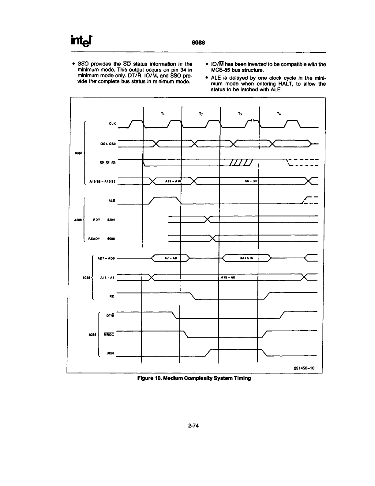
8088
SSO provides the S(5 status information in the • IO/M has been inverted to be compatible with the
minimum mode. This output occurs on pin 34 in MCS-85 bus structure.
minimum mode only. DT/R, IO/M and §SS pro- .
ALE js de| d b one clock |e jn the mjnj
.
v.de the complete bus status in
m.n.mum
mode.
mum mod
e when entering HALT, to allow the
status to be latched with ALE.
Figure 10. Medium Complexity System Timing
2-74
8088
ABSOLUTE MAXIMUM RATINGS*
Ambient Temperature Under Bias ... .0°C to + 70°C
Case Temperature (Plastic) 0°C to + 95°C
Case Temperature (CERDIP) 0°C to + 75°C
Storage Temperature - 65°C to +150°C
Voltage on Any Pin with
Respect to Ground -1.0 to +7V
Power Dissipation 2.5 Watt
* Notice: Stresses above those listed under "Abso-
lute
Maximum
Ratings" may
cause
permanent
damage to the device. This is a stress rating only and
functional operation of the device at these or any
other
conditions
above those indicated in the
opera-
tional sections of this specification is not
implied.
Ex-
posure to absolute maximum rating conditions for
extended periods may affect device
reliability.
D.C. CHARACTERISTICS
(TA
= 0°C to 70°C,
TCASE
(Plastic) = 0°C to 95°C,
TCASE
(CERDIP) = 0°C to 75°C)*
(VCc = 5V ±10% for 8088, VCc = 5V ±5% for 8088-2)
Symbol
V|L
V|H
V0L
V0H
»CC
»LI
ILO
VCL
VCH
QN
c,
0
Parameter
Input Low Voltage
Input High Voltage
Output Low Voltage
Output High Voltage
8088
Power Supply Current: 8088-2
P8088
Input Leakage Current
Output and I/O Leakage Current
Clock Input Low Voltage
Clock Input High Voltage
Capacitance If Input Buffer
(All Input Except
AD0-AD7,
RQ/GT)
Capacitance of I/O Buffer
AD0-AD7, RQ/GT)
Mln
-0.5
2.0
2.4
-0.5
3.9
Max
+ 0.8
VCc + 0.5
0.45
340
350
250
±10
±10
+ 0.6
vCc+ 10
15
15
Units
V
V
V
V
mA
JLlA
JLtA
V
V
PF
PF
Test Conditions
(Notel)
(Notes 1,2)
IOL
=
2.0 mA
IOH=
-400 |aA
TA = 25°C
0V £ V,N £ V
CC
0.45V
<;
VQUT
^ V
CC
fc = 1 MHz
fc = 1 MHz
NOTES:
*For Extended
Temperature
EXPRESS
Vcc = 5V ±5%
1.
V|L tested
with
MN/MX
Pin = 0V
V|H tested
with
MN/MX
Pin - 5V
MN/MX
Pin is a
strap
Pin
2. Not
applicable
to
RQ/STO
and
RT5/5TT
Pins
(Pin 30 and 31)
2-75

8088
A.C.
CHARACTERISTICS
(TA = 0°C to 70°C,
TCASE
(Plastic) = 0°C to 95°C,
TCASE
(CERDIP) = 0°C to 75°C)*
(VCc = 5V ±10% for 8088, VCc = 5V ±5% for 8088-2)
MINIMUM COMPLEXITY SYSTEM TIMING REQUIREMENTS
Symbol
TCLCL
TCLCH
TCHCL
TCH1CH2
TCL2CL2
TDVCL
TCLDX
TR1VCL
TCLR1X
TRYHCH
TCHRYX
TRYLCL
THVCH
TINVCH
TILIH
TIHIL
Parameter
CLK Cycle Period
CLK Low Time
CLK High Time
CLK Rise Time
CLK Fall Time
Data in Setup Time
Data in Hold Time
RDY Setup Time into 8284
(Notes 1,2)
RDY Hold Time into 8284
(Notes 1,2)
READY Setup Time
into 8088
READY Hold Time
into 8088
READY Inactive to CLK
(Note 3)
HOLD Setup Time
INTR.NMI,
TEST Setup Time
(Note 2)
Input Rise Time (Except CLK)
Input Fall Time (Except CLK)
8088
Min
200
118
69
30
10
35
0
118
30
-8
35
30
Max
500
10
10
20
12
8088-2
Mln
125
68
44
20
10
35
0
68
20
-8
20
15
Max
500
10
10
20
12
Units
ns
ns
ns
ns
ns
ns
ns
ns
ns
ns
ns
ns
ns
ns
ns
ns
Test
Conditions
From 1.0V to 3.5V
From 3.5V to 1.0V
From 0.8V to 2.0V
From 2.0V to 0.8V
2-76
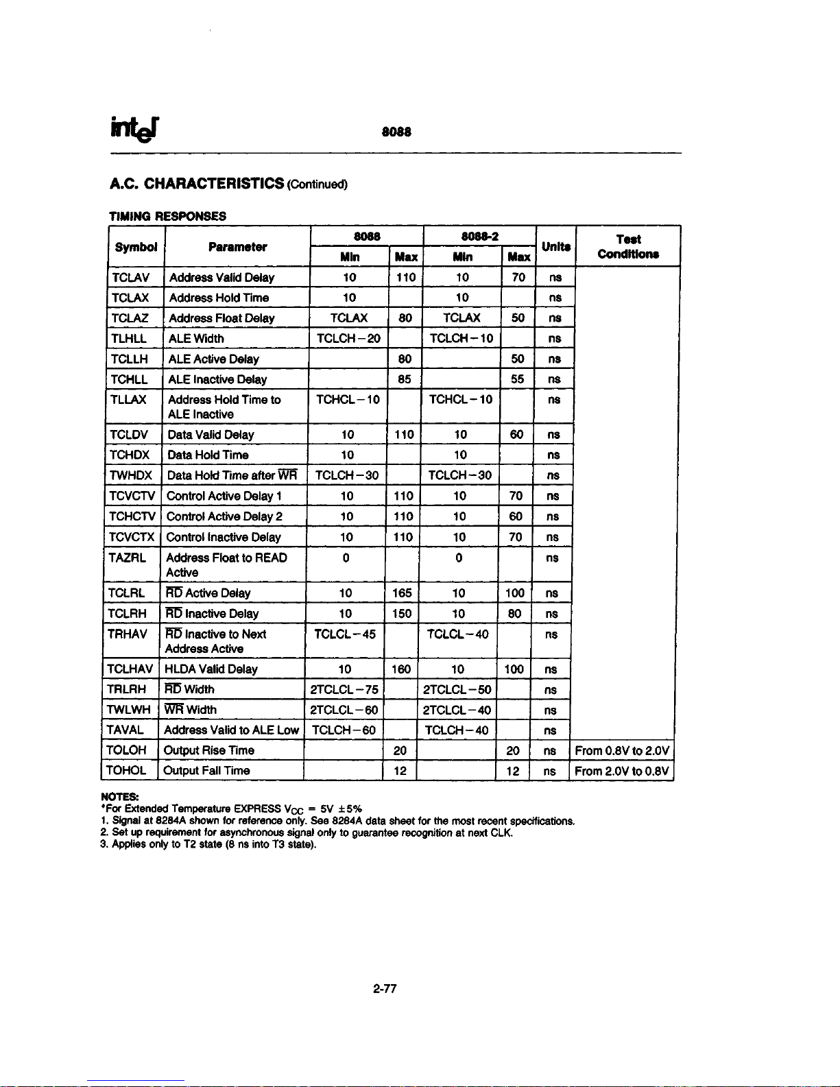
8088
A.C.
CHARACTERISTICS (Continued)
TIMING RESPONSES
Symbol
TCLAV
TCLAX
TCLAZ
TLHLL
TCLLH
TCHLL
TLLAX
TCLDV
TCHDX
TWHDX
TCVCTV
TCHCTV
TCVCTX
TAZRL
TCLRL
TCLRH
TRHAV
TCLHAV
TRLRH
TWLWH
TAVAL
TOLOH
TOHOL
Parameter
Address Valid Delay
Address Hold Time
Address Float Delay
ALE Width
ALE Active Delay
ALE Inactive Delay
Address Hold Time to
ALE Inactive
Data Valid Delay
Data Hold Time
Data Hold Time after WR
Control Active Delay 1
Control Active Delay 2
Control Inactive Delay
Address Float to READ
Active
RD Active Delay
RD Inactive Delay
RD Inactive to Next
Address Active
HLDA Valid Delay
RD Width
WR Width
Address Valid to ALE Low
Output Rise Time
Output Fall Time
8088
Min
10
10
TCLAX
TCLCH-20
TCHCL-10
10
10
TCLCH-30
10
10
10
0
10
10
TCLCL-45
10
2TCLCL-75
2TCLCL-60
TCLCH-60
Max
110
80
80
85
110
110
110
110
165
150
160
20
12
8088-2
Mln
10
10
TCLAX
TCLCH-10
TCHCL-10
10
10
TCLCH-30
10
10
10
0
10
10
TCLCL-40
10
2TCLCL-50
2TCLCL-40
TCLCH-40
Max
70
50
50
55
60
70
60
70
100
80
100
20
12
Units
ns
ns
ns
ns
ns
ns
ns
ns
ns
ns
ns
ns
ns
ns
ns
ns
ns
ns
ns
ns
ns
ns
ns
Test
Conditions
From 0.8V to 2.0V
From 2.0V to 0.8V
NOTES:
•For Extended Temperature EXPRESS VCc = 5V ±5%
1.
Signal at 8284A shown for reference only. See 8284A data sheet for the most recent specifications.
2.
Set up requirement for asynchronous signal only to guarantee recognition at next CLK.
3. Applies only to T2 state (8 ns into T3 state).
2-77

8088
A.C.
TESTING INPUT, OUTPUT WAVEFORM A.C. TESTING LOAD CIRCUIT
WAVEFORMS
BUS TIMING—MINIMUM MODE SYSTEM
2-78
 Loading...