


OEM
OPERATING
AND
SERVICE
MANUAL
TM848-1
AND
TM848-2
DISK
DRIVES
48
TRACKS
PER
INCH
'anCion
CORPORATION
20320
PRAIRIE STREET
CHATSWORTH, CA
91311
TELEPHONE
NO.: (213)
993-6644
TWX NO.:
910
494
1721
TEL.EX NO.:
194794
COPYRIGHT
1982
TANDON CORPORATION

The
information
containedinthis
documentisthe
property
of
Tandon Corporation. It may
notbeduplicated
in fullorpart
by
any
person
without
prior
written
approval. The material in
this
documentisprovided
for
informational
purposes,
andissubject
to
changebyTandon Corporation.

Sectoon
Number
SECTION
I
TABLE
OF
CONTENTS
TitleofSection
INTRODUCTION
TOTHETM848
FAMILYOF
DISKDRIVES
Page
Number
1.
1.1
1.2
1.3
1.4
1.5
1.6
1.7
1.8
1.9
1.10
1.10.1
1.10.2
1.10.3
1.11
1.12
1.13
1.14
1.15
1.15.1
1.15.2
1.15.3
1.15.4
1.15.5
1.16
1.16.1
1.16.2
1.17
1.17.1
1.17.2
1.17.3
1.18
1.19
1.19.1
1.19.2
1.19.3
1.19.4
1.19.5
1.19.6
1.19.7
1.19.8
1.19.9
1.19.10
1.19.11
1.19.12
1.19.13
1.19.14
1.19.15
1.19.16
1.19.17
Introduction
1-1
PurposeOfThe
Drive
1-1
Physical
DescriptionofThe
Drive
1-1
Functional
DescriptionofThe
Drive
1-1
Diskettes
1-2
Mechanical
and
Electrical
Sepcifications
1-2
Power
Requirements
1-2
Interface
Circuit
Specifications
1-2
Incoming
Inspection
Checks
and
Procedures
1-2
Interface
Connections
1-5
Mounting
The
Drive.." " ,
1-5
Hardware
"1-6
Dust
Cover.
1-6
Cooling
System
Requirements
1-6
Diskette
Care,
Handling
and
Storage
1-6
Write
Protect.
1-7
OperationofThe
Drive
1-7
OrganizationofThe
Drive
1-7
ComponentsofThe
Drive
'"
1-7
Index
Pulse
" , "
1-8
Drive
Status
Logic
"
1-8
Spindle
Drive
System
1-9
Positioner
Control
"
1-9
Data
Electronics
1-9
Interface
Electronics
"
'"
1-12
Interface
Connector
Pin
Assignments,
P13
1-12
Power
Connector
Pin
Assignments
1-12
Terminated
Lines
1-14
Input
Line
Terminations
From
Removable
Resistor
Pack
1-14
Drive
Select.
1-14
Program
Shunt
1-14
DS
and
HL
Power
Save
Options
1-17
User-Selectable
Options
1-17
Drive
Select
DS1--DS4
,
1-18
Side
Select
Options
Using
Drive
Select
18--48
1-18
In
Use
From
Drive
Select
1-18
In
Use
From
Head
Load
"
'"
1-18
Ready
Alternate
Output
Pad
1-18
Radial
Ready..'"
'"
1-19
Ready
Modified
1-19
Radial
Index
"
1-19
I
ndex
Alternate
Output
Pad
1-20
In
Use
Altenate
Output
Pad
1-20
Diskette
Lever
Lock
Latch
Option
1-20
Disk
Change
1-20
Two-Sided
Diskette
Installed
1-20
Stepper
Power
From
Drive
Select
1-21
Stepper
Power
From
Head
Load
Line
, 1-21
Head
Load
Alternate
Output
Pad
Option
1-21
Radial
Head
Load
Signal
Option
1-21

Section
Number
TitleofSection
Page
Number
1.19.18
1.19.19
1.19.20
1.19.21
1.19.22
Inhibit
Write When
Write
Protected
, 1-21
Allow
Write
When
Write
Protected
1-21
Head
Side
Select
Options
S1-S3
,
1-22
Spindle
Motor
Control
Options
M1 -
M4
1-22
Motor
Control
Select
Options
MC1 -
MC4
1-22
SECTION
II
MAINTENANCE
CHECKS
AND
ADJUSTMENTS
2.
Introduction
2-1
2.1
Spindle
Drive
Motor
Checks
and
Adjustments
2-1
2.1.1 Long-Term Drive
Motor
Speed
Checks
and
Adjustments
,
2-1
2.2
Cats
Eye
Alignment
Check
and
Adjustment
2-2
2.2.1
Cats
Eye
Alignment
Check
2-4
2.3
Head
Carriage
Adjustment
2-5
2.4
Index
Sensor
Checks
and
Adjustments
2-6
2.4.1 Index-To-Data Burst
Checks
2-6
2.4.2
Index
Sensor
Adjustment
, 2-7
2.4.3
Index
Pulse Width
Check
2-8
2.5 Track
00
Sensor
Check
and
Adjustment
2-8
2.6
Amplitude
Check
2-9
2.7
Azimuth
Check
2-10
2.8
Load
Arm
Adjustment
2-10
SECTION
III
PRINTED
CIRCUIT
BOARD
OPERATION
3.
3.1
3.2
3.3
3.4
Introduction
3-1
Physical
DescriptionofThe
Circuit
Board
3-1
Interface
Electronics
Specifications
3-1
Input
Control
Lines
3-2
Output
Control
Lines
3-7
SECTION
IV
TROUBLESHOOTING
GUIDE
4.
4.1
4.1
4.3
4.4
4.5
4.6
4.7
Introduction
" "
.,
"..4-1
Not
Ready
and/or
No
Index
,..4-2
Will
Not
SeekorRestore
4-2
Will
Not
Write
4-3
Will
Not
Read
4-3
Activity
L.E.D.
Inoperative
4-3
No
Track00Sensor
Indication
4-4
Drive
Motor
Will
Not
Start
When
Door
Latched
4-4
SECTION V REPLACEMENT PROCEDURES
5.
Introduction
5-1
5.1
Drive
Belt
5-1
5.2 Drive
Motor
5-2
5.3
Circuit
Board 5-3
5.4
Cone
Assembly
5-4
5.5
Diskette
Lever
, " 5-6
5.6
Bridge
Assembly
5-6
5.7 Bezel 5-8
ii

Section
Number
TitleofSection
Page
Number
5,8
5,9
5,10
5,'11
5,12
5,13
5,'14
5,'15
5,'16
5,'17
5.'18
ActivityL,E,
D",.
, " , " , . ,","""
, . ,.,, . "
., .,",..
, . , ,, . ,. , "
",.,, 5-9
Load
Arm
Assembly,.,..
, , , ,. , ,, . , ,, , ,, , .,
...
, , , ,. , ., , . , , , , ,. , ,. , . ,.., . , .
5-10
Track00Sensor
Assembly,
,, , ,, , ,. , , ,, . ,, , . ,, . ,. , . , ,..,.., , . , ., , ., , , .
5-10
Write
Protect
Sensor
Assembly,
,, , ,. , ,, , , ,, , ., , . ,. ,..,.., 5-11
Door
Switch
Assembly.., , , ,.., , . , ,, , , , ,
5-12
Index
Sensor
Assembly.,.,.., , , .,.,, "..,
5-12
Diskette
Ejector
Assembly
, , , ,,.., , , , , ,
5-14
Load
Resistor
Assembly,
, , , ,. , ,, , .,,.., , , . ,
5-15
Stepper
Band,
, , , , , , , , , ,..,, ,
5-16
Stepper
Motor
Assembly
,.,,.., , ,
.,
, , ,
5-18
Head
Carriage
Assembly""
..
"",
..
" , , ,
5-19
APPENDIX I PRINTED CIRCUIT BOARD SCHEMATICS AND
ASSEMBLY
DRAWiNGS"",
".,."",
, " , ,
1-1
APPENDIXIIRECOMMENDED
SPARE PARTS LIST , ".., ,
11-1
iii

LIST
OF
ILLUSTRATIONS
FIGURES
Figure
Number
TitleofFigure
Page
Number
1-1
TM848
Disk
Drive
Mounting
Configuration
" 1-6
1-2
TM848
Disk
Drive
Functional
Block
Diagram " 1-9
1-3 FM
Recording
Magnetization
Profiles
1-10
1-4
Write
Operation
Timing Diagram 1-11
1-5 Read Timing Diagram
1-12
1-6
Circuit
Board
Assembly
" " '
1-15
1-7
General
Control
and
Data Timing
Requirements
,..,
1-16
1-8 Radial Ready
Installation.." " "
1-19
1-9 Radial I
ndex
Installation
1-20
1-10
Radial
Head
Load
Signal. 1-21
2-1
Circuit
Board
Assembly
2-2
2-2
Hub
Center
Line
and
Track
Locations
2-3
2-3
Cats
Eye Pattern 2-4
2-4
Head
Module
Retaining
and
Cam
Screws
2-5
2-5
Index-to-Data
Burst.." , 2-7
2-6
Index
Sensor's
Retaining
Screw
and
Adjustment.
2-7
2-7
Negative
Going
Pulse
Width
2-8
2-8
Track
00
Sensor
2-9
2-9
Optimum
Head
Azimuth
Alignment.
2-11
2-10
Head
Azimuth
Alignment
Acceptable
Lower
Limits
2-11
2-11
Head
Azimuth
Alignment
Acceptable
Upper
Limits
, 2-12
2-12
Load
Arm Adjustment,
Front
View 2-12
3-1
Printed
Circuit
Board
3-1
3-2
Interface
Configuration
3-1
3-3
S~lect
Lines
Schematic
Diagram 3-2
3-4
Write
Data
Circuit
Block
Diagram 3-6
3-5 Trim Erase Diagram 3-8
3-6 Side
Select
Schematic
Diagram 3-9
3-7
Index
Schematic
Diagram , 3-11
3-8 Waveform
at
Test Point7,Soft
Sectored
3-11
3-9
Track
00
Schematic
Diagram
3-12
3-10
Write
Protect
Schematic
Diagram " "
3-13
3-11 Read
Circuit
Block
Diagram " "
3-14
3-12
Read
Data
Schematic
Diagram
3-15
5-1
Drive
Belt
and
Spindle
5-2
5-2 Drive
Motor
and
Related Parts 5-3
5-3
Circuit
Board
Mounting
Screws
" 5-4
5-4
Cone
Assembly
Key Parts 5-5
5-5
Cone
Assembly
Parts 5-5
5-6
Diskette
Lever
Key
Parts 5-6
5-7
Diskette
Lever
Adjustment
5-7
5-8
Bridge
Assembly
Key
Parts " 5-7
5-9
Bridge
Assembly
Additional
Key
Parts " 5-8
iv

Figure
Number
TitleofFigure
FIGURES
Page
Number
5-10
Bezel
and
Related Parts 5-8
5-1
"I
Activity
L.
E.
D.
Key
Parts 5-9
5-12
Load
Arm
Assembly
Key
Parts
5-10
5-13
Track00Sensor
Assembly
Key
Parts 5-11
5-14
Write
Protect
Sensor
Assembly
Key
Parts
5-12
5-15
Door
Switch
Assembly
Key
Parts
5-13
5-16
Index
Sensor
Assembly
Key
Parts, Top View
5-13
5-17
Index
Sensor
Assembly
Key
Parts,
Bottom
View
5-14
5
5-18
Diskette
Ejector
Assembly
Key
Parts ,
5-15
5-19
Load
Resistor
Assembly
and
Key
Parts
5-16
5-20
Stepper
Band
Key
Parts
5-17
5-21
Stepper
Band
Additional
Key
Parts
5-18
5-22
Stepper
Motor
Assembly
Key
Parts
5-19
5-23
Head
Carriage
Assembly
Key
Parts
5-20
TABLES
Table
Number
TitleofTable
Page
Number
1-1
1-2
1-3
1-4
1-5
3-1
3-2
Mechanical
and
Electrical
Specifications
1-3
Power
Requirements
1-4
Interface
Connector
Pin
Assingments
1-13
Power
Connector
Pin
Assignments
1-14
Options
1-17
Drive
Interface
Lines
and
Pin
Connectors
'"
,
3-3
Stepper
Logic
Truth Table
3-5
v

SECTION
I
INTRODUCTION
TO
THE
TM848
FAMILY
OF
DISK
DRIVES
1.
INTRODUCTION
This
section
containsadescriptionofthe
physical and
functional
specifications
forthe
TM848-1
and-
2
disk
drives,48tracks
per
inch (TPI),
manufacturedbyTandon
Corporation.
1.1
PURPOSE
OF
THE DRIVE
The drive is an
eight-inch
disk
memory
designed
for
random
access
data
entry, storage,and retrieval
applications. These
applications
typically
are
intelligent
terminal
controllers,
microcomputers,
word
processing
systems,
data
communications
systems,
error
logging,
microprogram
loading, point-of-
sale terminals,
and
Winchester
back
ups.
The drive is
capableofrecording
and reading
digital
data, using FM,
and
MFM.
1.2 PHYSICAL DESCRIPTION
OF
THE DRIVE
The drive
canbemountedinany
verticalorhorizontal
plane. However,
when
mounted
horizontally,
the
printed
circuit
board
must
be up.
The
spindleisbelt
drivenbya
brushless
D.C.
motor
withanintegral
tachometer.
The
servo
control
circuit,
suitably
sized pulleys, and
the
tachometer
control
the
speedofthe
spindle. The Read/Write,
double-sided
head
assemblyispositionedbymeansofa
stepper
motor,
split
band,
and
a pulley.
The
Read/Write/Erase
head
assembly
is a
glass-bonded
manganese/zinc
ceramic
structure.Ithas a
life in
excessof20,000
hours.
For
diskette
loading,
operator
access
is provide via a
slot
locatedonthe
frontofthe
drive.
The
electronic
componentsofthe
drive are
mounted
on a
circuit
board
assembly
locatedinthe
chassis.
Power
and
interface
signalsarerouted
through
connectors
that
plug
into
the
back
ofthe
drive.
1.3 FUNCTIONAL DESCRIPTION
OF
THE DRIVE
The drive is
fully
self-contained.
It requires
no
operator
intervention
during
normal operation. The
drive
consistsofa
spindle
drive
system, a head
positioning
system,
andaread/write/erase
system.
The TM848-1 is a
single-sided
drive. The
TM848-2
is a
double-sided
drive. The
only
difference
between
the
two
drives is
the
numberofheads. The
circuit
boardisidenticalinboth
models.
When
the
diskette
lever
is opened,
accessisprovided
for
the
insertionofa
diskette.
The
diskette
is
accurately
positionedbyplastic
guides.The
disk
positionisensuredbythe
backstop
and
disk
ejector.
Closing
the
diskette
lever
activates
the
cone/clamp
system,
resultingincenteringofthe
diskette
and
clampingofthe
diskettetothe
drive hub. The
drive
hub
is drivenata
constant
speedof360
RPMbya
servo-controlled
brushlessD.C.
motor. The head is
loaded
into
contact
with
the
recording
medium
whenever
the
diskette
lever
is latched.
1-1

The head is
positioned
over
the
desired
trackbymeansofa
stepper
motor/band
assembly
and
its
associated
electronics. This
positioner
employs
a 3.6
degree
rotationtocauseaone-track
linear
movement.
Whenawrite-protected
disketteisinserted
into
the
drive,
the
Write
Protect
sensor
disables
the
write
electronicsofthe
drive,
andaWrite
Protect
status
output
signal is availabletothe
interface.
When
performingawrite
operation, a
0.013-inch
wide
(nominal)
data
track
is recorded. This
track
is
then
tunnel
erasedto0.012
inch
(nominal).
Data
recovery
electronics
include
a low-level head amplifier, a
differentiator,azero
crossing
detector,
and
digitizing
circuits.
No
data-clock
separation
is provided.
In addition,
the
drive is
supplied
with
the
following
sensor
systems:
1.Atrack00sensor
that
senses
when
the
Head
Carriage
AssemblyispositionedatTrack
00.
2.
The
two
index
sensors, eachofwhich
consistsofa L.E.D.
light
source
andaphototransistor,
are
positionedsothat
a signal is
generated
whenaindex
holeisdetected.
The drive can
determine
whether
asingle-ordouble-sided
diskette
is installed. This
output
signalis
present
at
the
interface.
3.
The
Write
Protect
sensor
disables
the
drive's
write
electronics
wheneverawrite-enable
tab
is
removed from
the
diskette
(see
Section
1.12).
1.4 DISKETTES
The drive
usesastandard
eight-inch
diskette.
Diskette$
are available
withasingle
index
hole
orwith
index
and
sector
holes.
They
also are available
double-orsingle-sided.
Single
index
hole
diskettes
are used
when
sector
informationispre-recordedonthe
diskette
(soft
sectoring).
Multiple
index
hole
diskettes
provide
sector
pulsesbymeansofthe
index
sensor
and
electronics
(hard sectoring).
1.5
MECHANICAL
AND ELECTRICAL SPECIFICATIONS
The
mechanical
and
electrical
specificationsofthe
drive are listed in Table 1-1.
1.6 POWER REQUIREMENTS
The
power
requirementsofthe
drive
are
listed
in Table 1-2.
1.7 INTERFACE CIRCUIT SPECIFICATIONS
The
interface
circuits
are
designedsothatadisconnected
wire
results
in a false signal.
Levels:
True
=
+0.4V,maximum
False
=
+2.4V,minimum
1.8
INCOMING
INSPECTION
CHECKS
AND PROCEDURES
There are
two
kindsofrecommended
incoming
inspection
checks
and
procedures:
static
and
dynamic
ones.
The
static
incoming
inspection
checks
include
the
minimum
steps
that
should
be
takentoensure
that
the
driveisoperational
when
received.
1-2

TABLE
1-1
MECHANICAL
AND
ELECTRICAL
SPECIFICATIONS
MECHANICAL
Height:
2.30
inches
Width: 8
inches
ELECTRICAL
+ 5 V
D.C.Power:
+24VD.C.Power:
Selected
Motor
On:
Deselected:
Spindle
Motor:
Start
Current
Surge:
ENVIRONMENTAL
Operating
Temperature:
Storage
Temperature:
Wet
Bulb
Temperature:
Noncondensing
Operating
Humidity:
RELIABILITY
MTBF:
MTTR:
Error
Rates:
Soft
Read:
Hard
Read:
Seek
Errors:
PERFORMANCE
Head
Wear
Guarantee:
NumberofTracks:
Track-To-
Track
Access
Time:
Head
Settling
Time:
Average
Access
Time,
including
head
settling
time:
Motor
Start
Time:
Disk
Rotational
Speed:
I
nstantaneous
Speed
Variation:
Flux
Changes
Per
Inch,
Inside
Track:
Transfer
Rates:
Unformatted
Recording
Capacity:
IBM
Format
Recording
Capacity:
Recording
Method:
1-3
Length:
13.125
inches
behind
front
panel
Weight:
5.5
pounds
+5
volts
± 5 percent,
0.75
amp
typical
+24
volts±10
percent
0.75
amp
typical
0.20
amp
typical
OAO
amp
typical
2.5 amps,
400
msec
on,
24
volts
total
4.4°Cto46°C
(40°Fto115°F)
-40°C
to
71°C
(-40°F
to
160°F)
26°C (78°F)
maximum
20-to-80
percent
10,000
power-on
hours
30
minutes
1 in
109bits
1 in
1012bits
1 in
106seeks
15,000
media
hours
77
for
TM848-1;
154
for
TM848-2,
77
per
surface
3
milliseconds
15
milliseconds
91
milliseconds
700
milliseconds
360
RPM
± 1.0
percent
6536
FCI,
Side0,both
models;
6818
FCI,
Side1,TM848-2
only
250K
BPS
single
density,
500K
BPS
double
density
0.8 M
Bytes
per
disk,
single
density,
double-sided
drive
1.6
MBytes
per
disk,
double
density,
double-sided
drive
0.6
MBytes,
single
density,
double-sided
drive
1.2 MBytes,
double
density,
double-sided
drive
FM
single
density, MFM
double
density

TABLE 1-2
POWER REQUIREMENTS
1.
+5
Volts:
0.70
Amps
typical
2.
+24
Volts:
After
motor
start
interval
Spindle
Motor
0.35
Amps
typical
Stepper
Motor
0.40
Amps
typical
Electronics
0.17 Amps
typical
Total
0.92
Amps
typical
3.
+24
Volts:
During
motor
start
interval
a.
Configured
for
stepper
motor
enabled
during
motor
start.
2.5 Amps
typical
surge.
2.5
(j)
2.0
a..
~
~
~
1.5
z
w
a:
a:
1.0
::::>
()
0.5
"
\..
100
200
300
400
TIME (MILLISECONDS)
b.
Configured
for
stepper
motor
disabled
until
motor
comes
up
to
speed.
2.1
Amps
typical
surge.
500
600
600
500
400
300
200
100
I STEPPER MOTOR
ENABLED
"
V
~
I
•
2.5
en
2.0
a..
~
~
~
1.5
z
w
a:
a:
1.0
::::>
()
0.5
TIME (MILLISECONDS)
1-4

A.
Inspect
the
shipping
package
for
obvious
damage.
B.
Open
the
shipping
container,
and
remove
the
drive.
C.Inspect
the
drive's overall appearance. Ensure
that
there
arenoscratches
on
the
bezel.
D.
Ensure
that
all
internal
connectors
are
seated
properly.
E.
Turn
the
diskette
lever
counterclockwise,
and
remove
the
shipping
diskette.
F.
Insertablank
diskette,
close,
and
then
open
the
diskette
lever. The
diskette
should
eject.
G.
Insertablank
diskette,
and
manually
turn
the
spindle
pulley.Itshould
rotate
freely.
The
dynamic
incoming
inspection
procedures
include:
A.
Connect
the
drivetoan
exerciserorcomputer
tester
capableofseeking,writing,
and
reading.
B.
Power
up
the
test
equipment,
and
apply
powertothe
drive.
C.
Select
the
drive,
and
ensure
that
the
Activity
L.E.D.
located
on
the
bezel
illuminates.
D.Insertawork
diskette
and
write/verify
from Track00to
Track
76.
Ensure
that
there
are
no
errors.
E.
I
nsertadiskette
written
previouslyonanother
drive. Read
this
diskette,
and
ensure
that
there
arenodata
errors. If
excessive
errors
occur,
check
the
disketteonthe
driveonwhichitwas
written.
F.Ifthe
drive passes all
the
checks
listed
above, it is operational. If not, review
Section
II.
1.9 INTERFACE
CONNECTIONS
Signal
connections
for
the
drive are
made
via a
user-supplied
50-pin,
flat
ribbon
connector
(3M
Scotchflex
3415). This
connector
mates
directly
with
the
circuit
board
connectoratthe
rearofthe
drive. TheD.C.
power
connector
is a six-pin
connector
(Amp
Mate-N-Lok
Part
Number
1-480270-0),
which
mates
with
the
connectoratthe
rearofthe
drive.
Thesignal
connector
harness
shouldbeof
the
flat
ribbon
ortwisted
pair
type, havea maximum
length
of
ten
feet,
and
have a
22-to-28
gauge
conductor
compatible
with
the
connector
thatistobeused.
Power
connections
should
be
made
with
18-AWG cable, minimum.
1.10
MOUNTING
THE DRIVE
The drive has
been
designedtomountinany
plane,
Le.:
upright, horizontal,orvertical. The
only
restrictionisthat
the
printed
circuit
board
sideofthe
chassis
mustbeuppermost
when
the
drive is
mounted
horizontally.
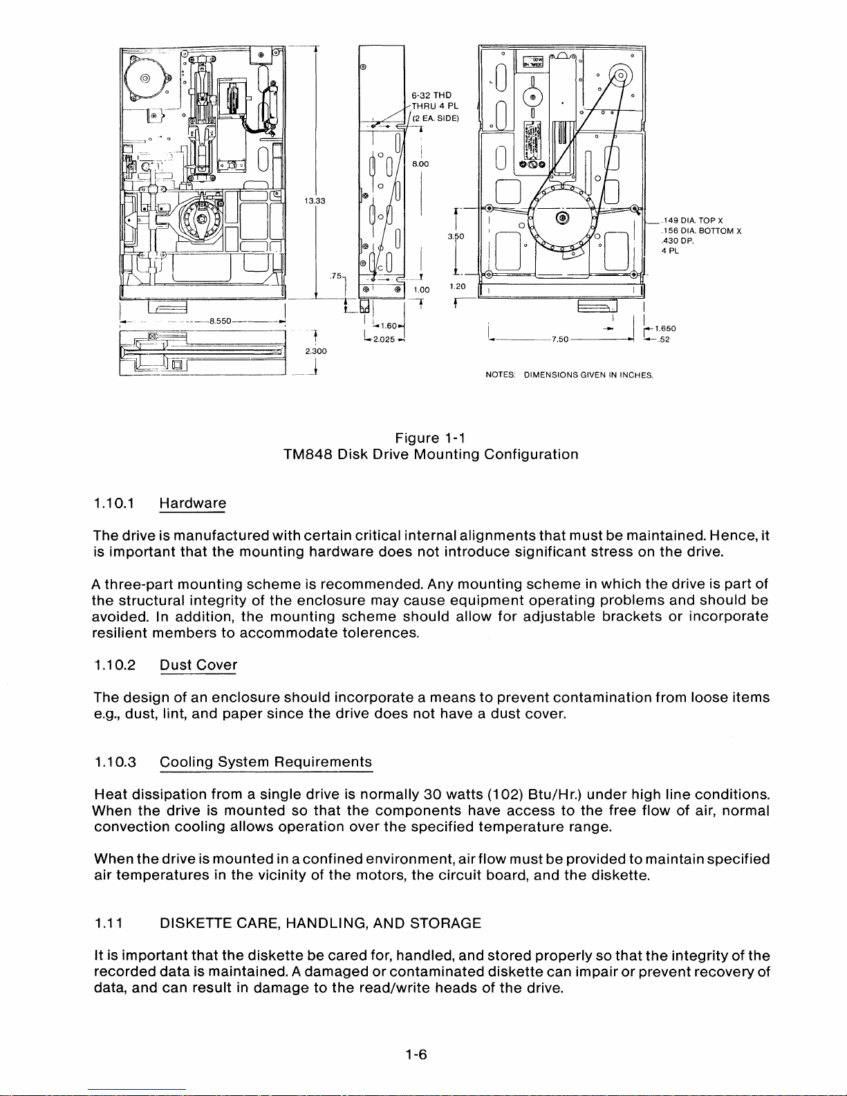
Eight
holes
are
provided
for
mounting:
twooneach
side
and
fouronthe
bottom
of
the
housing
(see Figure 1-1). The
two
on each
side
are
tapped
for
8-32
screws. The
four
mounting
holesonthe
bottom
require
8-32
thread
forming
screws.
Optional
straps
areavailabletopermit
attaching
two
drives
together
for
installationinstandard
width
drive openings.
1-5
---
0"
~-
°
F_}-
0r.!l\'l.
~1P.iI1r=--'t1
13.33
[(
J I
~-
-··------8.550----~
e
~
..
+
6-32 THO
THRU 4 PL
(2
EA.
SIDE)
I---r-'-~
-,
8.00
.149
DIA. TOP X
.156
DIA.
BOnOM
X
.430DP.
4 PL
I
L----7.50---~.1
t
1
..
::
0
NOTES:
DIMENSIONS
GIVENININCHES.
1.10.1
Hardware
Figure
1-1
TM848
Disk
Drive
Mounting
Configuration
The
driveismanufactured
with
certain
critical
internal
alignments
that
mustbemaintained.
Hence,
it
is
important
that
the
mounting
hardware
does
not
introduce
significant
stress
on
the
drive.
A
three-part
mounting
schemeisrecommended.
Any
mounting
schemeinwhich
the
driveispart
of
the
structural
integrityofthe
enclosure
may
cause
equipment
operating
problems
and
should
be
avoided.
In
addition,
the
mounting
scheme
should
allow
for
adjustable
brackets
or
incorporate
resilient
memberstoaccommodate
tolerences.
1.10.2
Dust
Cover
The
designofan
enclosure
should
incorporateameanstoprevent
contamination
from
loose
items
e.g.,
dust,
lint,
and
paper
since
the
drive
does
not
haveadust
cover.
1.10.3
Cooling
System
Requirements
Heat
dissipation
fromasingle
driveisnormally
30
watts
(102)
Btu/Hr.)
under
high
line
conditions.
When
the
driveismounted
so
that
the
components
have
access
to
the
free
flowofair,
normal
convection
cooling
allows
operation
over
the
specified
temperature
range.
When
the
driveismounted
in a
confined
environment,
air
flow
mustbeprovidedtomaintain
specified
air
temperatures
in
the
vicinityofthe
motors,
the
circuit
board,
and
the
diskette.
1.11
DISKETTE
CARE,
HANDLING,
AND
STORAGE
It
is
important
that
the
diskette
be
cared
for,
handled,
and
stored
properlysothat
the
integrityofthe
recorded
dataismaintained.Adamagedorcontaminated
diskette
can
impairorprevent
recovery
of
data,
and
can
resultindamagetothe
read/write
headsofthe
drive.
1-6

The
following
list
contains
information
on
how
the
diskette
can be
cared
for, handled,
and
stored.
1.
Keep
the
diskette
away
from
magnetic
fields.
2.
Do
not
touch
the
precision
surfaceofthe
diskette
with
fingers.
3.
Insert
the
diskette
carefully
into
the
drive
until
the
backstopisencountered.
4.
Do
not
bendorfold
the
diskette.
Ei.
Put
the
diskette
into
its
jacket
when
it is
not
in use.
6.
Store
the
disketteattemperatures
between1DoC
and 52°Cor50°F
and
125°F.
1.12 WRITE PROTECT
The drive is
equipped
withaWrite
Protect
Sensor
Assembly.This
sensor
operatesinconjunction
with
a
diskette
that
has a
slot
cutinthe
protective
jacket.
When
the
slot
is uncovered,
the
disketteiswrite
protected.
The
slot
mustbecoveredtowriteonthe
diskette.
An
option
is available on
the
board
for
defeating
the
write
protect
sensor.
1.13 OPERATION
OF
THE DRIVE
The drive
consistsofthe
mechanical
and
electrical
components
necessarytorecord
andtoread
digital
dataona
diskette.
User-providedD.C.
powerat+24
volts
and+5voltsisrequired
foroperation
of
the
drive.
1.14 ORGANIZATION
OF
THE DRIVE
All
electrical
subassembliesinthe
drive
are
constructed
with
leads
that
terminate
in
multipin
connectors,
enabling
the
individual
assembliestobe removed.
The
heads
are
connectedtothe
circuit
board
via
cables
that
terminate
in five-pin
female
connectors
and
their
associated
male
sockets
that
are
located
in
close
proximity
to
the
read/write
data
electronics.
Interface
signals
and
power
are
provided
via
connectorsatthe
rearofthe
drive.
1.15
COMPONENTS
OF
THE DRIVE
The drive
consistsofsix
functional
groups:
'1.
Index
Pulse
Shaper
2.
Drive
Status
Logic
A.
Write
Protect
B.
Track
00
Sensor
C.
Double-sided
Disk
D.
Ready
E.
Disk
Change
1-7

3.
Spindle
Drive
Control
4.
Carriage
Position
Control
5.
Write/Erase
Control
6.
Read
Amplifier
and
Digitizer
Figure
1-2
is a
functional
block
diagramofthe
drive.Itshouldbereferredtoin
conjunction
with
the
following
sections.
The
datainthe
ensuing
figuresisprimarily
representedinsimplified
form.
1.15.1
Index
Pulse
An
index
pulseisprovidedtothe
user
system
via
the
index
pulse
interface
line.
The
index
circuitry
consistsofan
indexL.E.
D.,anindex
phototransistor,
andapulse
shaping
network.Asthe
index
hole
in
the
disk
passesanindex
L.E.D.
phototransistor
combination,
light
from
the
L.E.D.
strikes
the
index
phototransistor,
causingitto
conduct.
The
signal
from
the
index
phototransistorispassedonto
the
pulse
shaping
n~twork,
which
producesapulse
for
each
hole
detected.
This
pulseispresentedtothe
useronthe
index
pulse
interface
line.
1.15.2
Drive
Status
Logic
There
are
five
drive
status
logic
lines:
Write
Protect,
Track00Sensor,
Two-Sided
Ready
and
Disk
Change.
A.
Write
Protect
A
write
protect
signalisprovidedtothe
user's
system
via
the
write
protect
interface
line.
The
write
protect
circuitry
consistsofa
write
protect
sensor
and
circuitry
that
routes
the
signal
thatisproduced.
Whenawrite
protected
disketteisinsertedinthe
drive,
the
sensorisactivated
and
the
logic
disables
the
write
electronics
and
supplies
the
status
signaltothe
interface.
B.
Track
00
Sensor
The
levelonthe
Track
00
interface
line
is a
functionofthe
positionofthe
head
assembly.
When
the
headispositionedatTrack00and
the
stepper
motorisat
the
home
position,atrue
(low) level
signalisgeneratedatthe
interface.
C.
Two-Sided
Disk
This
signalislow
(true)
when
the
driveisselected
and
has
detected
the
presenceofthe
Index
Two
holeinthe
diskette
currently
installed.
D.
Ready
This
signalistrue
when
Drive
Selectislow
(true)ifthe
spindle
driveisuptospeed
and
the
driveisreadytoread
and
write.
E.
Disk
Change
This
signalistrue
when
Drive
Selectislow
(true) if
the
diskette
lever
has
been
movedtothe
open
position
after
the
previous
drive
select
went
false.
1-8

1.15.3
Spindle Drive System
The spindle drive system consists of a spindle assembly driven through a drive belt by a brushless
D.C. motor/tachometer.
The servo electronics required for speed control are located on the printed circuit board.
The control circuitry contains an interface
control
line.
When
the drive motor control interface line
is
false (high), the drive motorisallowed to come up to speed.
READY
CONTROL
INDEX
LOGIC
DISK
CHANGE
TWO SIDED
WRITE PROTECT
TRACK
00
IN USE
SIDE SELECT
HEAD CARRIAGE
DRIVE SELECT
AND STEPPER
BAND
ASSEMBLY
SPINDLE
MOTOR
CONTROL
MOTOR
CONTROL
WRITE GATE
WRITE
WRITE DATA
LOGIC
CURRENT
SWITCH
READ READ DATA
LOGIC
DIRECTION
STEPPER
MOTOR
CONTROL
STEP
Figure
1-2
TM848
Disk Drive Functional Block Diagram
1.15.4
Positioner Control
The head positioning system uses a bipolar-driven motor drive, which changes
one
phase for each
track advancement of the read/write carriage. In addition to the logic necessary for motor control, a
gateisprovided that inhibits positioner motion during a write operation.
1.15.5 Data Electronics
Information can be recorded
on
the diskette by using a double-frequencycode. Figure
1-3
illustrates
the magnetization profiles
in
each bit cell for the number sequence shown for FM recording.
1-9

BIT
PATTERN----,
BIT
CELL""""
I 1 I 1
I I I
I I I
WRITE
DATA
o
I
I
1
I
C D
ic
D IC C I
D
C
ICC
D
1
I
I
I
I I I
I I I I I I
I I I
\:f.=k:1
,-,t;fl:f
~t:A1
I f I
MAGNETIZATION
1:
1
I I -
~
.
~
--'I
I
~
I I
IIIIIIIIIII~II
M~NEnCELEMEN~
~
I
r--rTt4
I I
Figure 1-3
FM
Recording
Magnetization
Profiles
The
erase
gaps
provide a
guard
band
on
either
sideofthe
recorded
track.
All
signals
requiredtocontrol
the
data
electronics
are providedbythe
user
system
and
are
shown
in
the
TM848
drive
functional
block
diagram (see
Figure
1-2). These
control
signals
are:
1.
Select
2.
Write
Gate
3.
Write
Data
4.
Side
Select
5.
Write
Current
Switch
Composite
read
dataissenttothe
user
system
via
the
Read
Data
interface
line.
A.
Data
Recording
The
write
electronics
consist
ofaswitchable
write
current
source, a
write
waveform
generator,
an erase
current
source,
the
trim erase
control
logic, and
the
head
selection
logic
(see
Appendix
I).
The
read/write
windingonthe
head is
center-tapped.
Duringawrite
operation,
current
from
the
write
current
source
flowsinalternate
halvesofthe
winding,
under
controlofthe
write
waveform generator.
The
conditions
required
for
recording,
i.e.
drive ready
must
be
established
by
the
user's
system, as follows:
1.
Drive
speed
stabilization
occurs
700
milliseconds
after
the
drive
motor
is started.
2.
Subsequenttoany
read/write
operation,
the
positioner
must
be
allowedtosettle. This
requires18milliseconds
maximum
after
the
last
step
pulse
is initiated,
i.e.,3milliseconds
for
the
step
motion
and
15
milliseconds
for
settling.
3.
The
foregoing
operations
can be overlapped, if required.
Figure
1-4
illustrates
the
timing
diagram
forawrite
operation. At t =0,
when
the
unit
is ready,
the
write
gate
interface
line
goes
true. This
enables
the
write
current
source.
Write
current
is
switched
via
the
write
current
switch
interface
linetoa
lower
valuebythe
user's
controller
at
Track 43.
1-10

The Trim Erase
control
goes
true
190
microseconds
after
the
Write
Enable
interface
line
since
the
trim erase
gaps
are
behind
the
read/write
gap. It
shouldbenoted
that
this
value is
optimized
between
the
requirementsatTrack00andatTrack
76,sothat
the
effectofthe
trim
erase
gaps
on previous
information
is minimized.
Figure
1-4
shows
the
informationonthe
write
data
interface
line
and
the
outputofthe
write
waveform
generator,
which
togglesonthe
leading
edgeofevery
write
data
pulse.
A maximum
of4microseconds
between
write
gate
going
true
and
the
first
write
data
pulse
is
only
requirediffaithful
reproductionofthe
first
write
data
transition
is signifcant.
At
the
endofrecording,atleast
one
additional
pulseonthe
write
data
line
mustbeinserted
after
the
last
significant
write
data
pulsetoavoid
excessive
peak
shift
effects.
3.
10MAPEAKTO PEAK, TRACK 0 TO
TRACK42; 7.5 MAPEAK
TO
PEAK,
TRACK
43
TO TRACK 77.
4.
2 USEC
MINIMUM
4 USEC MAXIMUM
I
I
NOTES:
1.
T = 0 =
700
MILLISECONDS
AFTER DRIVE MOTOR
STARTS OR
20
MILLISECONDS
AFTER LAST STEP
PULSE, WHICHEVER IS THE LATEST TIME.
2.
UNSYCHRONIZED
Figure
1-4
Write
Operation
Timing Diagram
NOTE 2
I
~
I
~50usec""
I I
~-""""""-----""---"""~:;-"'I~
~---tl----;---+----
........-
.......
-~
.......
I
~~
I I
WRITE
WAVEFORM
GENERATOR
WRITE
CURRENT
INTERNAL WRITE
BUSY
TRIM ERASE
WRITE GATE
The
durationofa
write
operation
is from
the
true
going
edgeofwrite
gatetothe
false
going
edge
of
erase. This is
indicatedbythe
internal
write
busy
waveform
shown
(see Figure 1-4).
The Read
electronics
consist
of:
1.
Read
Switch/Side
Select
2.
Read
Preamplifier
3.
Filter
4.
Differentiatior
5.
Time
Domain
Filter
and
Digitizer
The read
switch
is usedtoisolate
the
read
amplifier
from
the
voltage
excursion
across
the
head
duringawrite
operation. The
side
select
is usedtoenable
oneofthe
read/write/erase
heads.
Thedrive
must
be in a ready
condition
before
readingcan begin.As
with
the
data
recording
operation,
this
ready
condition
must
be
established
by
the
user
system. In
addition
to
the
requirements
establishedinthis
section, a periodof100
microsecondsisnecessary
after
a trim
erase
operation
occurstoallow
the
read
amplifiertosettle
after
the
transient
causedbythe
read
switch
returning
to
the
read mode.
1-11

The
output
signal from
the
read/write
headisamplifiedbya read
preamplifier
and
filteredbya low-
pass
linear
phase
filtertoremove
noise
(see Figure 1-5). The
linear
output
from
the
filter
is passed
to
the
differentiator,which
generates
awaveform
whose
zero
crossovers
correspondtothe
peaksofthe
Read signal. This signal is then fedtothe zero crossing detector and digitizer.
LINEAR OUTPUT FROM FILTER
OUTPUT FROM DIFFERENTIATOR
READ DATA INTERFACE
t
t
==
0
Figure 1-5
Read Timing Diagram
Note
T= 0 is
definedas250
milliseconds
after
drive
motor
starts,or20
milliseconds
afterastep
command,or100
microseconds
afterterminationofwrite
busy,
whicheveristhe
latest
time.
The
zero
crossover
detector
and
digitizer
circuitry
generatea200
nanosecond
read
data
pulse,
correspondingtoeach
peakofthe
read signal. The
composite
read
data
signal is
senttothe
user
system via
the
read
data
interface
line.
1.16 INTERFACE ELECTRONICS
All
interface
signals
are TTL compatible.
Logic
true
(low) is
+0.4
volt maximum,
logic
false (high) is
+2.4
volts
minimum. The maximum
interface
cable
lengthisten
feet.Itis
recommended
that
the
interface
cable
be flat ribbon
cable
that
has a
characteristic
impedenceof100
ohms.
1.16.1
Interface
Connector
Pin Assignments, P13
The
interface
connector
pin assignments, P13, are listed in Table 1-3.
1.16.2
Power
Connector
Pin
Assignments
The
power
connector
pin
assignments
are listed in Table 1-4.
1-12

TABLE
1-3
INTERFACE
CONNECTOR
PIN
ASSIGNMENTS
Ground
---
1
3
5
7
9
"11
'13
"15
"17
'19
:21
:23
:25
27
29
31
33
35
37
39
41
43
45
47
49
Pin
Number
2
4
6
8
10
12
14
16
18
20
22
24
26
28
30
32
34
36
38
40
42
44
46
48
50
Signal
Write
Current
Switch
Motor
Off
Control
1
Motor
Off
Control
2
Motor
Off
Control
3
Two
Sided
(option)
(Model
TM848-2
only)
Disk
Change
(option)
Side
Select
(Model
TM848-2
only)
ActivityIndicator
(option)
Head
Load
Index
Ready
Motor
Off
Control
4
Drive
Select1(Side
Select
Option,
TM848-2
only)
Drive
Select2(Side
Select
Option,
TM848-2
only)
Drive
Select3(Side
Select
Option,
TM848-2
only)
Drive
Select4(Side
Select
Option,
TM848-2
only)
Direction
Select
(Side
Select
Option,
TM848-2
only)
Step
Write
Data
Write
Gate
Track
00
Write
Protect
Read
Data
Alternate
I/O
Alternate
I/O
1-13

TABLE 1-4
POWER CONNECTOR PIN
ASSIGNMENTS
Pin
1
6
3
2
5
1.17 TERMINATED LINES
Supply
Voltage
24VD.C.
Return
Return
Return
5V
D.
C.
1.17.1
Input
Line
Terminations
From Removable Resistor Pack
The drive
has
the
capabilityofterminating
the
following
input
lines:
1.
Write
Current
Switch
2.
Write
Data
3.
Write
Gate
4.
Side
Select
(TM848-2
only)
5.
Direction
6.
Step
7.
Head
Load
These
input
lines
are
individually
terminated
througha150
ohm
resistor
pack
thatisinstalledinthe
dip
socket
locatedatintegrated
circuit
location
RP1. In a single-drive system,
this
resistor
pack
shouldbeinstalledtoprovide
the
proper
terminations. In a multiple-drive system,
only
the
last drive
on
the
interfaceisto
be terminated. All
other
drivesonthe
interface
must
have
the
resistor
pack
removed (see
Figure
1-6).
1.17.2 Drive
Select
The
Select
lines
provide
a meansofselecting
and
deselecting
a drive. These
four
Iines·-OS1
through
DS4--allow
independent
selectionofuptofour
drives
attachedtothe
controller.
When
the
signal
logic
level is
true
(low),
the
drive
electronics
are
activated
and
the
drive is
conditionedtorespondtoStep
orto
Read/Write
commands.When
the
signal
logic
level isfalse(high),
the
input
control
lines
and
the
output
status
lines
are disabled.
The drive
select
addressisdetermined
by
a movable
shorting
plug
installed
on
the
circuit
board.
Select
lines
one
through
four
provide a
meansofdaisy
chaining
a maximumoffour
drivestoa
controller.Onlyonelinecan betrue(low) at a time.An undefined operation might result iftwo
or
moreunits
areassigned
the
sameaddressoriftwoormoreselect linesare in the true(low) state simultaneously (see
Figure
1-7). A
select
line
must
remain
stableinthe
true
(low)
state
until
the
execution
if a
Step
or
Read/Write
commandiscompleted.
1.17.3 Program Shunt
The program shunt is AMP Part Number 435704-8. The program shunt positions are programmed by
cutting
the
particular
shunt. The program
shunt
is installed in a
dip
socket. At
the
user's option,
the
program
shunt
may
be removed
and
replacedbya
dip
switch. Pins 8 and 9ofthe
program
shunt
are
not
used.
See
Table 1-5
fora
listingofthe
program shunts.
1-14

R133
o
P6
P14
M2
00
o
o
00
00
CI:(J)
CI:O
~P4
~P5
M3
0-0
o
M4
2SCH)
DC
00
00
RI
TP11 G 0 TP12
ALTERNATE TEST POINT, INDEX TRIGGERING
R33
I
00
y
~
NP
@O~S2
OS1
g~O:
WP
P2
P3
Pi0
Pi
P11
P12
TP5
t
TP4ooopT6
TP2
TP1
1
o
~o
TP3
P8
pg
00
DSi
1b
0
000S2
2b
0
000S3
3b
0
000S4
4b
0
o
OTP8
OTP10
gOL
P7
MC3
2 j
MC2~C'gMC1
S2
0
IT
S
1
D 0 S2
o
C g
MC4g
RP1
o
TP9
P13
50
TP7
o
......
I
......
01
Figure 1-6
Circuit Board Assembly

D.C. POWER
MOTOR OFF
CONTROL
DRIVE SELECT
---l
r-
500
NSEC. MINIMUM
0,8 SEC
MAXIMUM
..
_
STATUS
OUTPUTS VALID
-
........
"'1--
500
NSEC'MINIMUM
---.:.J
L 1 USEC MINIMUM
~-------
..
DIRECTION
SELECT
I---
550
USEC.
MINIMUM'
4 USEC.
MAXIMUM
I--
100
USEC. MAXIMUM
U3 MILLISECONDS
MINIMUM
1 USEC. J
l--
MINIMU~~
I---
100
NSEC MINIMUM.
...
---------
....
--
...
~~
.-U
I---
18
MSEC. MINIMUM
1--------_
......
-....
..-------'\,,...---.
~
VALID
READ DATA
WRITE DATA
SIDE SELECT
WRITE GATE
Figure 1-7
General Control and Data Timing Requirements
1-16

1.18
OS
AND
HL
POWER SAVE OPTIONS
The
driveis
setupwith
theHLoption
in. This
stepper
power
from head load
line
option
supplies
power
to
the
stepper
motor
when
the
head load
line
goes
low
(true),
which
resultsinlower
stand-by
current
consumption.
As
shipped
from
the
factory, HL is installed
but
will remove
power
from
the
stepper
motor
when
the
driveisdeselected.
There
should
be a
20
millisecond
wait
after
a Drive
Select
command
is given in
ordertoallow
the
step
motor
electronicstosettle.
The
stepper
power
from drive select,
OS
option,
allows
the
usertoremoveD.C.
power
from
the
stepper
motor
using driveselect,
which
resultsinlower
stand-by
current
consumption.
This
option
is
implemented
by
installing
OS,
and
cutting
HL.
1.19 USER SELECTABLE OPTIONS
The
descriptionofuser
selectable
options
should
be used in
conjunction
with
the
following
list
of
options
that
are
available
for
model
numbers
TM848-1 and
TM848-2
(see Table 1-5).
TABLE 1-5
OPTIONS
AS
SHIPPED
TRACE
Shunt/Pin
Not
OPTION
DESIGNATOR
Locations
Installed
Installed
Drive Se
lect
DS1-DS4
DS1
Side
Select
Options
using Drive
Select
1B-4B
X
In Use, Drive
Select
Z
U3,1-16
X
In Use,
Head
Load
Y
X
Ready
Alternate
Output
Pad
R
U3,
7-10
X
Radial Ready
RR
X
Ready,
Modified
RM
X
Radial
Index
RI
X
Index,
Alternate
Output
Pad
I
U3,6-11
X
In Use,
Alternate
Output
Pad
0 X
Diskette
Lever
Lock
Latch
Option
DL X
Disk
Change
DC X
Two-Sided
Diskette
Installed
2S X
Stepper
Power
from Drive
Select
OS
X
Stepper
Power
from
Head
Load
Line
HL
U3,2-15
X
Head
Load
Alternate
Output
Pad
C
X
Radial
Head
Load
Signal
A
U3,3-14
X
Radial
Head
Load Signal
B
U3,4-13
X
Radial
Head
Load
Signal
X
U3,5-12
X
I
nhibit
Write
When
Write
Protected
WP
X
Allow
Write
When
Write
Protected
NP X
Head
Side
Select
Options
S1-S3
S2
Spindle
Motor
Control
Options
M1-M4
M1,
M3
M2,
M4
Motor
Control
Select
MC1-MC4
MC1
1-17

1.19.1
Drive
Select
OS
1-DS4
This
option
allows
the
usertodaisy
chain
uptofour
drives,
andtoenable
one
driveatat
time.
Drive
selectisimplementedbyshorting
oneofthe
four
connections,
usingashorting
plug.
The
drive
comes
equipped
from
the
factory
with
OS1
installed.
All
outputs
are
gated
with
drive
select,asset-up
at
the
factory.
1.19.2
Side
Select
Options
Using
Drive
Select
18--48
This
option
allows
the
usertoselect
the
headtobe
used
with
drive
select.
Side
Select
options
are
implementedbyremoving
the
shorting
plug
from
the
DS1-DS4
option
pads,
installing
Pins18-48,
and
connecting
the
shorting
plugtothe
desired
18-48
pins. S2
shouldbeetch
cut,
and
S3
installed
(see
Section
1.18).
1.19.3 In
Use
From
Drive
Select
(Z)
This
option
allows
the
usertoenable
the
activity
L.E.D.
when
the
driveisselected.
In
Use
From
Drive
Selectisfactory
installed.
1.19.4 In
Use
From
Head
Load
(Y)
This
option
allows
the
usertouse
the
head
load
linetoenable
the
Activity
L.E.D.
In
Use
From
Head
Loadisimplemented
by
punching
out
OptionZbetween
Pins 1
and
16ofU3. A
jumper
must
be
installedatlocation
Y.
1.19.5
Ready
Alternate
Output
Pad
(R)
This
low
going
signalisderivedbygating
the
internal
ready
and
drive
selecttogive
the
controller
a
true
(low)
ready
statusofthe
drive
.
. The
Ready
Alternate
Output
Pad is
factory
installed.
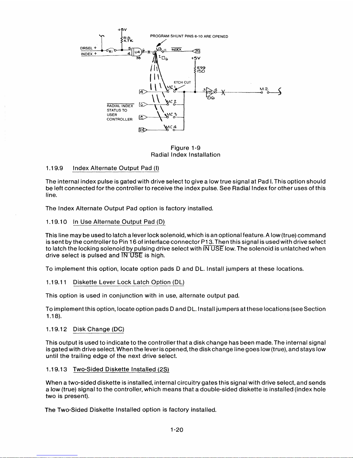
1.19.6 Radial
Ready
(RR)
This
option
allows
the
usertomonitor
the
ready
statusofall
drives
without
selecting
them.
This
option
cannot
be
used
concurrently
with
individual
motor
control
lines
for
each
drive.
(see
Figure
1-8).
Radial
Readyisimplementedbypunching
out
OptionRbetween
Pins 7
and10of
U3,byetch
cutting
RR,
thenbyrunningawire
from
U4, Pin 3tothe
desired
alternate
output
lines4,6,8,
and
24.
1-18

RI4
+5
~99
150
+5V
ETCH CUT
PROGRAM
SHUNT
PINS
7-10
ARE
OPENED
/'
OREDY+
RADIAL
READY
STATUS
TO USER
CONTROLLER
RM
'9
ETCH CUT
~-~~4
~
IREADY
-
,--
.........
--
~'3_SE_L_+_.
---~'--o-------'
RR
Figure
1-8
Radial Ready
Installation
Note
MC1
through
MC4
cannot
be used as radial
motor
control
when
using
this
option.
1.19.7
Ready,
Modified
(RM)
This
option
allows
the
drivetowriteonthe
upper
surfaceofa
single-sided
diskette. It
prevents
the
drivefrom
making
Ready
become
false
when
the
upper
surfaceofa
single-sided
diskete
isselected.
To
implement
this
option,
connectajumperatthe
RM pads.
1.19.8
Radial
Index
(RI)
This
option
uses
the
alternate
I/O
lines
for
radial
index
lines.This
option
allows
the
userto
monitor
the
indexofeach
drive
independentofdrive select. This
option
cannot
be used
concurrently
with
radial
ready,
or
with
independent
motor
control.
Radial
Indexisimplementedbyremoving
the
shunt
bridge
at U3, Pins 6
and
11, by
etch
cutting
radial
index,
andbyrunningawire
from U4, Pin6,to
the
appropriate
alternate
I/O
lines.IfuseofMC1 is
desired,
interface
line
20
may be used as
one
index
line. In
this
case,
the
shunt
pack, U3, 6-11,
remains
intact
on
one
drive, (see
Figure
1-9).
1-19
R.99
150
+~v
~
R\~
4.71(.
DRSEL + .... 5
INDEX
+
R\
D--e--=i
4
RADIAL INDEX
STATUS TO
USER
CONTROLLER
PROGRAM
SHUNT
PINS
6-10
ARE OPENED
/
1,l~"OI\
INDEX
QQ]
'LOCo
+5V
1/\
~\
'~
'\
ET_CH
CUT
\
t"f;,V
~
2-
[4
Q--
~It_-3r2!~X:------~
~
rr---, \ \
1fC
2.
OeD
~
\\
CD
','oMC
~
fM>
't'C4
Figure
1-9
Radial I
ndex
Installation
1.19.9
Index
Alternate
Output
Pad (I)
The
internal
index
pulse is
gated
with
drive
selecttogivealow
true
signalatPadI.This
option
should
be
left
connected
for
the
controllertoreceive
the
index
pulse.
See
Radial
Index
for
other
usesofthis
line.
The
Index
Alternate
Output
Pad
optionisfactory
installed.
1.19.10 In Use
Alternate
Output
Pad (D)
This linemaybeused
to
latchalever
lock
solenoid,
which
isan
optional
feature. A
low
(true)
command
is
sentbythe
controllerto
Pin16of
interface
connector
P13.Then
this
signal is
used
with
drive
select
to
latch
the
locking
solenoidbypulsing
drive
select
with IN USE low. The
solenoidisunlatched
when
drive
selectispulsed
and
IN
USE
is high.
To
implement
this
option,
locate
option
pads D
and
DL. Install
jumpersatthese
locations.
1.19.11
Diskette
Lever
Lock
Latch
Option
(DL)
This
option
is used in
conjunction
with
in use,
alternate
output
pad.
To
implement
this
option,
locate
option
padsD
and
DL.lnstall
jumpersatthese
locations
(see
Section
1.18).
1.19.12
Disk
Change
(DC)
This
output
is usedtoindicatetothe
controller
thatadisk
change
has
been
made. The
internal
signal
is
gated
with
driveselect.When
the
lever
isopened,
the
disk
change
line
goes
low
(true),
and
stays
low
until
the
trailing
edgeofthe
next
drive select.
1.19.13 Two-Sided
Diskette
Installed
(2S)
When a
two-sided
diskette
is installed,
internal
circuitry
gates
this
signal
with
driveselect,
and
sends
a
low
(true) signaltothe
controller,
which
means
thatadouble-sided
disketteisinstalled
(index hole
two
is present).
The Two-Sided
Diskette
Installed
optionisfactory
installed.
1-20
1.19.14
Stepper
Power
From Drive
Select
(OS)
This
option
allows
the
usertoremoveD.C.
power
from
the
stepper
motor
using
drive
select,
which
resultsinlower
stand-by
current
consumption.
The
Stepper
Power
From Drive
Select
optionisimplemented
by
installing
OS,
and
cutting
HL.
1.19.15
Stepper
Power
From
Head
Load
Line
(HL)
This
option
supplies
powertothe
stepper
motor
when
the
head load line
goes
low
(true).This
results
in
lower
stand-by
current
consumption.
This
optionisfactory
installed.
OS
must
be removed
for
proper
operation.
1.19.16
Head
Load
Alternate
Output
Pad
Option
C
This
option
allows
the
userto
loadand
unload
the
headload
solenoid
(optional) and,
along
with
the
HL
and Y options,
enables
the
stepper
motor
and
lights
the
Activity
L.E.D.,
respectively.
Head
load is
accomplished
by
connecting
both
option
padsClocated
near
interface
connector
P13.
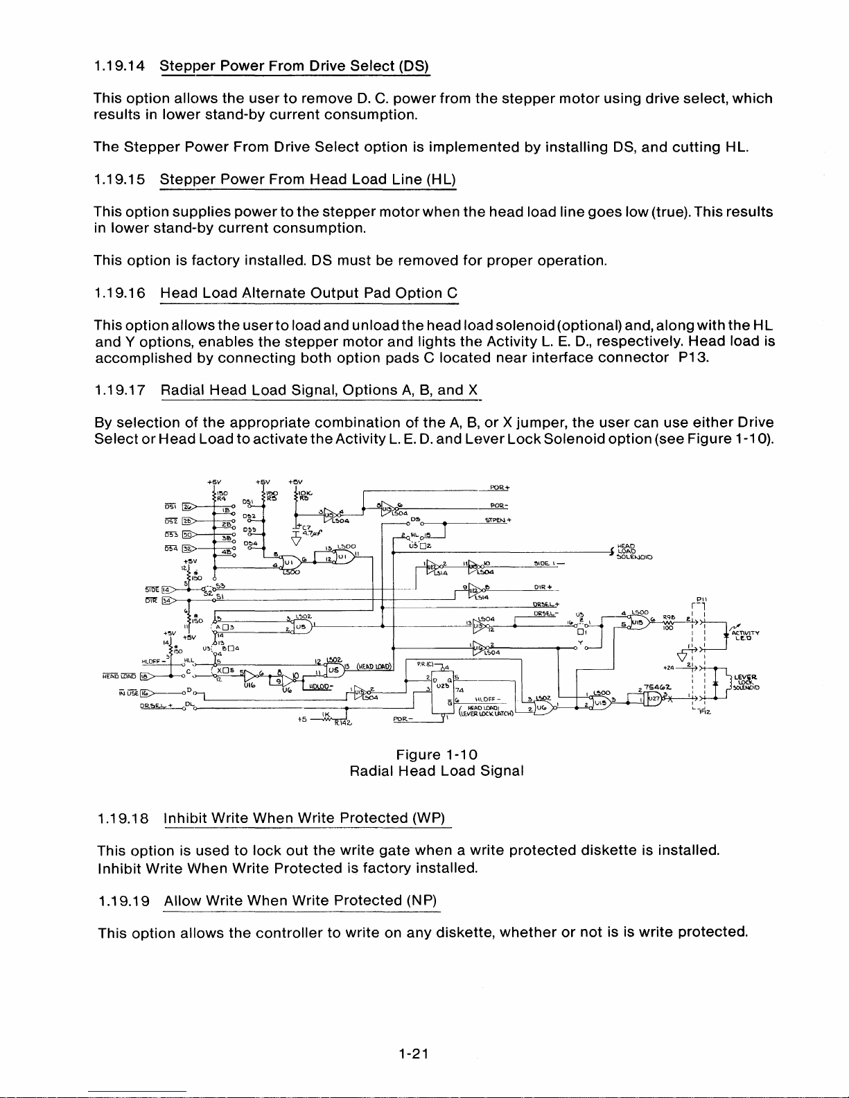
1.19.17 Radial
Head
Load
Signal,
Options
A,
B, and X
By
selectionofthe
appropriate
combinationofthe
A,B,or
Xjumper,
the
user
can use
either
Drive
SelectorHead
Loadtoactivate
the
Activity
L.E.D.
and
Lever
Lock
Solenoid
option
(see
Figure
1-10).
DIR±..._
OIl.~L..+
10 SlOE.
\-
W';ll..-
U,>
c==
I(,cr!!:'
0,
y
r#)O.O'----
__
--<>
POR.-
(i>
POR-
L504
D~
':iTI>El<.l+
H~;=r---
....-_uS_'O_z,
----ll
~getDID
,.--______
POR+
+SV
+5V
+ov
I~O
\'::>0
R4
RO
';f,~
5iDE
~--<1;i=:)'O'------------t-t--+_···_·,
~:14
,,"'_---O-,5~1
----------1--+-+-------'
ISO
tr~'------"'<1~
,.......L';,OZ.
11:1'.03
z.
US
)-'-1
---------+----~
+5V
+5V
14
14
I~
U~:,
4e04
5
Figure
1-10
Radial
Head
Load Signal
1.19.-18
Inhibit
Write
When
Write
Protected
(WP)
This
option
is usedtolock
out
the
write
gate
whenawrite
protected
diskette
is installed.
Inhibit
Write
VVhen
Write
Protectedisfactory
installed.
1.19.19
Allow
Write
When
Write
Protected(NP)
This
option
allows
the
controllertowriteonany
diskette,
whetherornot
is is
write
protected.
1-21

Note
This
option
does
not
stop
the
write
protect
signal from being
sentonthe
interface
line.
This
optionisimplementedbycutting
WP,
andbyinstalling NP.
1.19.20
Head
Side
Select
Options
S1--S3
This
option
allows
headstobe
selectedbyside
select, driveselect,
orthe
direction
control
signal.The
drive
comes
with
side
select, S2, installed.
To
use
the
drive
select
linetoenable
the
heads,
cut
S2
and
install S3
along
with
the
proper
18-48
jumper
that
is used with S3 (see
18-48).
For
head
selection
using
Direction
Select,
cut
S2, and install
S1.
1.19.21
Spindle
Motor
Control
OptionsM1--M4
M1 is usedtoenable
the
motor
off
delay
timer. When
this
jumper
is installed,
the
drive
motor
is
enabled
and
disabledbyeither
the
drive
select
(M3)orhead load (M4) commands. A
20-second
turn
turn
off
delayofthe
spindle
motorisactivated
on
the
trailing
edgeofthe
controlling
signal.
M2
is used
for
radial
motor
control
independent
ofthe
motor
control
functions
installed
withM1,
M3,
and M4.
M2
shouldbein
ifthe
user
wishestoenable
the
drive
motor
continuouslyorto
use
the
radial
motor
on
line MC1-MC4.
M3
is usedtocontrol
the
drive
motor
using
drive
select.
When
the
drive
select
line
goes
low
(true),
the
drive
motor
comesupto
speed
in less
then
500
milliseconds
and
becomes
ready in less
than
700
milliseconds.
After
the
drive
select
line
goes
false (high),
the
motor
will run
for
20
seconds. To
implement
this
option, install a
jumperatlocation
M3.
For
correct
operationofM3, remove M4.
M4
is usedtostart
the
drive
motor
using
the
head load
interface
lines.
When
the
head load
line
goes
low(true),
the
drive
motor
comesupto
speed
in less than
500
milliseconds
and
becomes
readyin less
than
700
milliseconds.
After
the
head load line
goes
high (false),
the
motor
will run
for20seconds.To
implement
this
option, remove
M3
for
correct
operationofoption
M4.
1.19.22
Motor
Control
Select
Options
MC1--MC4
This
option
is usedif
the
drive
motoristobeenabled
independentofdrive
selectorheadselect.
When
these
lines are
low
(true),
the
motor
is off. The drive
comes
without
this
option
installed. This
option
does
not
operate
the
time
out
delay
circuit.
To
implement
this
option
that
controls
the
drive
motor
usingan
MCx
line, install
the
appropriate
MC 1-
MC4
jumper.
When
using
this
option,
M2
must
be installed. If
the
motor
turn
off
delay
is desired,
the
delaycanbetriggeredbyDrive
SelectorHead
Load commands,
when
used in
conjunction
withM3or
M4.
1-22

SECTION
II
MAINTENANCE
CHECKS
AND
ADJUSTMENTS
2.
INTRODUCTION
This
sectionisfor
the
useofthe
OEM
Repair
Department.Itcontains
checks
and
adjustments
that
are
used
during
the
normal
lifeofthe
drive.
Before
applying
powertothe
driveordoing
any
checksoradjustments,
visually
inspect
the
drive
to
ensure
thatithasnomissingorbroken
parts.
The
following
equipmentisrequired
for
checks
and
adjustments:
1. A
dual-channel,
wideband
oscilloscope:
Tektronix
465orequivalent
2.
An
exerciserorsoftware
routine
capableofstepping
the
drivetoany
track,
selecting
the
upperorlower
head,
and
writing
a 1F,all
zeros
if FM,or a 2F, all
ones
if FM,
patternonthe
disk.
3. A
Phillips
screwdriver
4. A
setofAllen
wrenches
5.Aflat
blade
screwdriver
6.Ablank
diskette
7. An
alignment
diskette:
Dysan
PIN
360/2Aorequivalent
8.
Integrated
circuit
dip
clips,14and
16
pin
2.1
SPINDLE
DRIVE
MOTOR
CHECKS
AND
ADJUSTMENTS
The
long-term
drive
motor
speed
adjustment
ensures
that
the
motor's
speediswithin
the
range
of
tolerance
specified.
The
motor
speed
specificationis360
RPM ±
1.25
percent.
2.1.1.
Long-Term
Drive
Motor
Speed
Checks
and
Adjustments
A.
Preliminary
checks
required:
Verify
power:
+24VD.C.±10
percent
+5VD.C.
± 5
percent
B.
Apply
powertothe
drive.
C.
Activate
the
drive
motoronthe
interface
line.
D.Insertawork
diskette.
2-1

E.
Setupthe
oscilloscope, as follows:
Voltage: 2
volts
per
division
Time Per Division:
20
milliseconds
Trigger: Negative,
ChannelA,R33
Note
For
the
TM848-1 single-sided drive,
trigger
offofR33.
For
the
TM848-2
double-sided drive,
trigger
off of Test Point 12,
with
the
exceptionofazimuth,
which
must be
triggered
offofR33
(see Figure 2-1).
'
R133
MIg
0
8
M2
cr.
00
o
1ttttttttttttft
....
-.;.,;P6:.....-_-r-
P
,;"..,14
00
00
(I<Il
(IO
~
..
P4
~P5
M3
C>O
o
M4
2S_
DC
00
00
RI
~
ALTERNATE
TEST
POINT,INDEX
TRIGGERING
0-3-0
NP
00
y
DSI
00&00
DS2
WP -
TPll0erz.,.
P2
P3Pl0
PI
PllP12
ffiffftf11TTiil
TP2
TPI
1
-
Jo
TP3
P8 P9
1i1iftttif
00
DSI
lb
0
00
DS2
2b
0
00DS3
3b
0
00DS4
4b
0
o
OTP8
OTP10
gDL
P7
00
P13
Figure
2-1
Circuit
Board Assembly
F.
Adjust
R133
until
a reading
of
166.667
millisecondsisachieved
from leading
edgetoleading
edgeofthe
index
pulses.
G.Ifthe
drive motor's
speed
cannot
be adjusted,
see
Section
IV,
Troubleshooting
Guide.
2.2 CATS EYE
ALIGNMENT
CHECK
AND ADJUSTMENT
The
Cats
Eye
(C.
E.)
alignment
procedure
locates
the
read/write
headatthe
oroper
radial
distance
from
the
hub
center
line,
ensuring
that
the
track
location isaccurate(seeFig;ure 2-2). This
adjustment
is necessary
only
after
servicingorif
diskette
interchange
problems
are suspected.
2-2

HUB CENTER LINE
TRACK 0
"---~---
TRACK
38
TRACK
76
Figure 2-2
Hub
Center
Line and Track Locations
2-3

2.2.1
Cats
Eye
Alignment
Check
A.
Setupan oscilloscope, as follows:
Channel
A;
Channel
B:
Ground
Read Differentially:
Time Base:
External Trigger:
Test
Point2alternate
is Test
Point
4 on R30
Test Point 3
alternate
is Test Point 5 on R29
Test
Point
1
A plus
B,
B inverted
20
milliseconds
per
division
Test Point 11, negative trigger,
for
single-sided drives. Test
Point
12, negative trigger,
for
double-sided drives. R33 (end
closest
to
DS2), negativetrigger, isan
alternate
test
point
for
both
single-and
double-sided drives.
B.
Apply
powertothe
drive.
Note
TheTrack38radius is 2.8207 ± .0020.
Other
tracklocationsarecomputedbased upon48TPI.
C.
Select
the
driveatthe
interface.
D.
Insert
the
alignment
diskette
into
the
drive.
E.
Select
Head 00,
the
lower
head.
F.
Seektoand
observe Track38for
Cats
Eye
alignmentofthe
lower
head.
G.
Adjust
the
oscilloscopetoobserve a
Cats
Eye
pattern
(see Figure 2-3).
Equal amplitude.
Lobes
shownat100
percentonTrack
38.
Time Scale:
20
ms
Figure 2-3
Cats Eye Pattern
2-4

H.
Verify
that
the
smallerofthe
two
Cats
Eye
lobesisnot
less
than
75
percentinamplitude
of
the
other
one.
The
calculation
is:
ampofsmaller
lobe
X
100
ampoflarger
lobe
I.
Step
the
drivetoTrack
00, then,
stepitbacktoTrack
38.
J.
Reverify
the
Cats
Eye pattern.
K.
Step
the
drivetoTrack
76; then,
stepitbacktoTrack
38.
L.
Reverify
the
Cats
Eye pattern.
M.
On
double-headed
drives,
select
the
upper
head (Head 01)
and
repeat
StepsFthrough
L.
N.Ifanyofthe
checks
listed
above
does
not
meet
the
conditions
statedinStepH,the
head
carriage
must
be adjusted.
2.3 HEAD CARRIAGE
ADJUSTMENT
A.
Turn
the
two
position
retaining
screws
that
straddle
the
nylon
adjustment
cam
located
ben~ath
the
drive
until
the
cam
can be moved (see
Figure
2-4).
POSITION RETAINING SCREWS (2)
ADJUSTMENT CAM
Figure
2-4
Head
Module
Retaining
and
Cam
Screws
B.
Observe
the
Cats
Eye
pattern
from
the
head
thatisfarthest
outofalignment.
C.
Using a
flat
blade
screwdriver,
turn
the
adjustment
cam
until
one
Cats
Eye
lobeiswithin
75
percentoJthe
amplitudeofthe
other
lobe.
Note
Check
the
upper
and
lower
headsondouble-sided
drives (see
Section
2.2.1,
"F"
through
"l"
on
upper
head).
D.
Tighten
the
two
positioner
retaining
screws
(see Figure 2-4).
2-5

E.
Reverify
the
Cats
Eye
alignment
(see
Section
2.2.1).
2.4
INDEX
SENSOR
CHECKS
AND
ADJUSTMENTS
The
index
adjustment
changes
the
time
period
from
the
index
pulsetothe
startofthe
data.
The
adjustment
shouldbechecked
after
the
drive
has
been
aligned
(see
Section
2.1.1)orwhen
diskette
interchange
errors
are
suspected.
2.4.1
Index-to-Data
Burst
Check
A.
Apply
powertothe
drive.
B.
Select
the
drive.
C.
Check
the
spindle
speedofthe
drive
(see
Section
2.1).
D.
Setupan
oscilloscope
as
follows:
Trigger:
Read
Differentially:
Channel
A:
Channel
B:
Time
Base:
Single-sided
drives
trigger
on
right
leadofR33
(closest
to
DS2),
negative
edge;
double-sided
drives
trigger
on
Test
Point
12,
negative
edge.
A
plusB,B
inverted
Test
Point
2
Test
Point
3
50
microseconds
per
division
E.
Insert
an
alignment
diskette.
F.
SeektoTrack
1.
G.
Select
Head
00,
the
lower
head.
H.
Ensure
that
the
index-to-data
burst
occursat200
microseconds±100
microseconds
from
the
leading
edgeofthe
index
pulse
(see
Figure
2-5).
I.
For
double-sided
drives,
select
Head
01
and
repeat
the
steps
above.
Note
Head
01
should
meet
the
same
specification.
J. If
either
Head00or
Head01does
not
meet
the
specifications,
adjust
the
index
sensor
(see
Section
2.4.2.).
2-6

Time
Scale:
50
usee
per
division
Figure
2-5
I
ndex-to-Data
Burst
K.
When
both
index
measurements
on a
double-sided
driveorthe
one
index
measurement
on a
single-sided
drive
meet
the
specifications,
see
SectionH,check
the
index-to-data
burst
on
Track
76.
L.
On a
double-sided
drive,
check
Heads
01
and
00,
the
upper
and
lower
heads.
Note
If
any
index
measurement
does
not
meet
the
specification,
the
index
sensor
must
be
adjusted
(see
Section
2.4.2).
2.4.2
Index
Sensor
Adjustment
A.
Loosen
the
index
sensor's
retaining
screw
located
on
the
undersideofthe
chassis
(see
Figure
2-6).
o
o
L:)
.J
o
INDEX SENSOR
'P\6~1f""""H--H----
RETAINING SCREW
Figure
2-6
Index
Sensor's
Retaining
Screw
and
Adjustment
2-7

B.
Adjust
the
index
sensor
withaflat
blade
screwdriver
until
the
index-to-data
burst
occurs
200
microseconds±100
microseconds
from
the
leading
edgeofthe
index
pulse.
C.
Tighten
the
index
sensor's
retaining
screw.
D.
Reverify
the
index-to-data
bursts
(see
Section
2.3.1).
2.4.3
Index
Pulse
Width
Check
The
index
pulse
widthisnonadjustable.Ifthe
index
pulse
widthisnot
within
specifications,
replace
theIndex
Sensor
Assembly.
A.
Setupan
oscilloscope
as
follows:
Channel
A:
Ground:
Time
Base:
Voltage:
Trigger:
To
appropriate
index
test
point,
see
Section2,Item
Number
1.
Test
Point
1
.5
millisecond
per
division
2
volts
per
division
Negative
leading
edgeofChannel
A,
appropriate
test
point.
B.
Ensure
that
the
negative
going
pulse
widthisbetween
1.0
and
2.3
milliseconds
(see
Figure
2-
7).
u u
~
~
1.8to2.3
milliseconds
Figure
2-7
Negative
Going
Pulse
Width
2.5 TRACK00SENSOR
CHECK
AND ADJUSTMENT
TheTrack00sensor
providesa signal
that
identifiesTrack00to
the
logic
electronics.A
Track00signal is
senttothe
controller
on Pin20of
the
interface.
A.
Apply
powertothe
drive.
B.
Load an
alignment
diskette
into
the
drive.
C.
Step
the
carriagetothe
radial
alignment
track, Track38(see
Section
2.2).
2-8

D.
Confirm
the
positionbyobserving
the
Cats
Eye pattern.
E.
Attach
ChannelAto
Test Point 10.
F.
Restore
the
carriagetoTrack 00,
and
ensure
that
the
Track00L.E.D.onthe
exerciser
turnson.
G.
SeektoTrack1,and
ensure
that
the
signalatTest Point10is high.
H.
SeektoTrack2,and
ensure
that
this
lineisloworin
transition.
I.
SeektoTrack3,and
ensure
that
this
line is low.
J. If
the
signal is incorrect, restoretoTrack00with
the
oscilloscope
attached
as above.
K.
Seek
outtoTrack2,and
loosen
the
two
retaining
screws
that
hold
the
Track00sensor
(see
Figure 2-8).
RETAINING SCREWS
Figure
2-8
Track
00
Sensor
L.
Push
the
sensor
toward
the
backofthe
drive, and
slowly
push it forward until
the
signal on
the
oscilloscope
just
goes
low
(true).
M. Tighten
the
retaining screws,
and
repeat
StepsEthrough
I.
N.
Verify
the
adjustment.
2.6 AMPLITUDE
CHECK
The
amplitude
test
checks
the
necessary read,
channel
amplifier/differential
output
voltage.
A.
RestoretoTrack
00
B.
Insertawork
diskette
and
write
a 2F, all ones, pattern on
the
lower
head.
2-9

C.
Connect
an oscilloscopetoTest Points 4 and5,using Test Point 1 as a ground.
D.
Set up an oscilloscope as follows:
Channel
A:
Channel
B:
Both Channels:
Time Base:
Trigger:
Test Point
4,
1 volt per division
Test Point
5,
1 volt per division
A.C.coupled, Channels A and B added,
Channel B inverted
50
milliseconds per division,
synchronize internally on Channel A
or
B
Automatic
E.
The minimum amplitude displayed on the scope should be no less than three
(3)
volts peak-to-
peak at any point.
F.
Reverify
the
measurement with another
work
diskette.
G.
Check
the upper and lower head, if applicable.
H.
If the amplitude is less than the specification, inspect the heads
to
ensure they are
not
contaminated.
I.
Clean the heads with a cleaning diskette if they are contaminated.
J. Replace the circuit board if cleaning does not improve
the
amplitude.
K.
If replacing the circuit board does not correct the amplitude, replace
the
Head Carriage
Assembly.
2.7 AZIMUTH CHECK
Azimuth is the angle
of
the
heads with respect to the track at
the
point of
the
read/write gap. Azimuth is
measured in minutes (one minute
=
1/60
degree).
A.
Set up an oscilloscope as follows:
Channel
A:
Test Point2,100
mV
per
division
Channel
B:
Test Point3,100
mV
per
division
Ground: Test Point 1
Both Channels:
A.C.coupled, Channels A and B added,
Channel B inverted
Time Base: 1 millisecond
or
as required to display
the
pulse groups
Trigger: Leading edge of appropriate test point
(see Section
2,
Item Number
1)
B.
Insert an alignment diskette.
C.
Step
the
drivetoTrack
76'.
D.
Observe
the
following pattern. Figure 2-9depictsan optimum head alignment ofzero minutes of
azimuth error. This means that
the
Head Carriage Assembly is perpendiculartothe
track
being
read, Track 76. Bursts 1 and 4 are of equal amplitude; Bursts 2 and 3 are of equal amplitude.
2-10

Note
Measure
the
azimuth burst. Ensure that Burst 1
is less than
or
equaltoBurst2,and that Burst
4 is less
thanorequaltoBurst 3.
1 2
3
4
Figure 2-9
Optimum
Head
Azimuth
Alignment
E.
Figure
2-10
depicts
an azimuthofexactly
minus9,12,or18
minutes,
depending
upon
the
manufacturerofthe
diskette
used. This is
the
lower
limitofallowable
azimuth error.
Bursts
1 and 2 areofequal amplitude.Ifthis
signal is observed,
the
Cats
Eye
alignment
shouldbechecked
priortoany
corrective
action.
3'
1 2
4
Figure
2-10
Head
AzimuthofAcceptable
Lower
Limits
F.
Figure 2-11
depictsanalignmentofexactly
plus9,12,or18
minutes,
depending
upon
the
manufacturerofthe
diskette
used. Bursts 3 and 4 areofequal amplitude.This is
the
upper
limitofallowable
azimuth
error. If
this
signal is observed,
the
Cats Eye
alignment
shouldbechecked
priortoany
corrective
action.
G.
After
the
lower
head has been checked,
switchtoread on
the
upper
head and observe
the
azimuth pattern. Both
the
upper
and
lower
heads
shouldbewithin
the
specification.
2-11

2
3 4
1
Figure 2-11
Head Azimuth Alignment of Acceptable
Upper
Limits
Note
The head's azimuth is
not
adjustable.Itis suggested
that
the
drive be
senttoan authorized repair
centerora new Head assembly be installed. In
the
latter
case, all previous adjustments should be made again.
2.8 LOAD ARM ADJUSTMENT
This adjustment is made to ensure
proper
loadingofthe
head when
the
diskette
is engaged (see
Figure 2-12).
A.
Insert a
work
diskette
into
the drive.
B.
Turn the
diskette
leverto load
the
disk, and
seektoTrack00. There shouldbe aspaceof.015
inch minimum between
the
head load arm and
the
load plate.
C.
SeektoTrack 76, and ensure that a space of .015 inch minimum remains between
the
head
load arm and
the
load arm.
D.
Adjust
the
screw
located behind
the
head load cam until
the
foam
just
touches
the
platen.
E.
Inserta
work
diskette
and ensure
that
there is adequate space between
the
upperhead and
the diskette.
F.
The
upper
head should
not
hit
the
diskette
when inserting and ejecting it.
ADJUSTMENT SCREW
Figure 2-12
Load Arm Adjustment, Front View
2-12
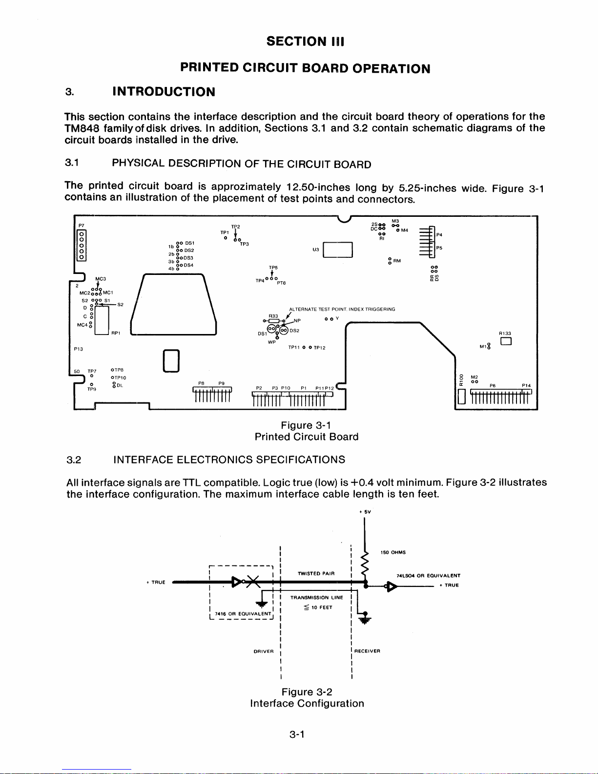
SECTION
III
PRINTED
CIRCUIT
BOARD OPERATION
3.
INTRODUCTION
This
section
contains
the
interface
description
and
the
circuit
board
theoryofoperations
for
the
TM848
familyofdisk
drives. In addition,
Sections
3.1
and 3.2
contain
schematic
diagramsofthe
circuit
boards installed in
the
drive.
3.1
PHYSICAL DESCRIPTION OF THE CIRCUIT BOARD
The printed
circuit
board is
approzimately
12.50-inches long by 5.25-inches wide. Figure
3-1
contains
an illustrationofthe
placementoftest
points
and connectors.
R133
M18
0
g
M2
a:.
00
P6 P14
o
ffitttttttttffl
00
00
a:CIl
a:c
~P4
~P5
M3
0-0
OM4
2SCH)
DC
00
00
RI
v
TP11 0 0 TP12
ALTERNATE TEST POINT. INDEX TRIGGERING
~I
NP
ooy
OS1Sg&S2
WP
TP5
t
TP4000pT6
P2
P3
P10
P1
P11P12
~
TP2
TP1
!
o
~O
TP3
00081
1b
0
000S2
2b
0
000S3
3b
0
00084
4b
0
P8
pg
9iffftttff
o
OTP8
OTP10
gOL
P7
00
P13
Figure
3-1
Printed
Circuit
Board
3.2 INTERFACE ELECTRONICS SPECIFICATIONS
All interface signals are
TIL
compatible.
Logic
true
(low) is
+0.4
volt minimum. Figure 3-2 illustrates
the
interface
configuration. The maximum interface
cable
length is
ten
feet.
+
5V
+
TRUE
r--------,
I I
I
I
I
I I
L
7~6
~~E~U~~~~
TWISTED
PAIR
TRANSMISSION
LINE
~
10
FEET
74LS04OREQUIVALENT
+
TRUE
DRIVER
RECEIVER
Figure 3-2
Interface Configuration
3-1

Itisrecommended
that
the
interface
cablebeflat
ribbon
cable,
withacharacteristic
impedance
of
100
ohms.
Interface
connector
pin
assignments
are
given
in Table 3-1.
3.3 INPUT
CONTROL
LINES
A.
DS1-DS4,
Select
Lines
Functional
Description
The
select
lines
(see
Figure
3-3) provide a
meansofselecting
and
deselecting
a drive. These
four
lines, DS1
through
DS4,
select
oneofthe
four
drives
attachedtothe
controller.
When
the
signal
logic
level is
true
(low),
the
drive
electronics
areactivated,
and
the
driveis
conditionedtorespondtoStep
or
Read/Write
commands.
When
the
logic
level is false (high),
the
input
control
lines
and
output
status
lines
are
disabled.
POR+
PII
"
L':>OO
r-1
15(o11.9f>
2.
D
100 I I
I I
~nVIT'(
I I L.E.O.
~I
VI
I
+Z4~ID'
I I LEVER
I I
LOC.~
2.
754(,,2.
I I
~NO\D
" I
I
2.7
L_J
PIZ,
'lEl'.D
t-------------~
LOAD
~LEt-.lOIO
DR':>E.l..-
U~
c==
llocr~\
01
t------'-Io
I)c~--
__
--oy
~-
J .
_\4
g~~
011>+
---+-+-+--
'il
!2.
e.
DIR+_
L':lI.q
+~V
+5V
1'50
R!:>
+sv
150
R4
Figure
3-3
Select
Lines
Schematic
Diagram
A
select
line
must
remain
stableinthe
true
(low)
state
until
afteraSteporRead/Write
command
has
been
executed.
The drive
select
address
(1-4) is
determined
by
shorting
plugsonthe
circuit
board.
Select
lines
1
through4provide
a meansofdaisy
chaining
a maximumoffour
drivestoa controller.
Only
one
line
can be
true
(low)ata time. An
undefined
operation
might
result if
twoormore
units
are
assigned
the
same
addressorif
twoormore
select
lines
areinthe
true
(low)
state
simultaneously.
Circuit
Description
An
150-ohm
resistor
holds
the
outputofthe
appropriate
Select
line high (false)
until
the
line
is driven
low
(true). Then,
the
Select
signal is
gated
throughU1andUSto
derive
the
signal
DRSEL+.DRSEL+
is usedtogate
all
I/O
Port,
ensuring
that
only
one
drive's
dataispresentonthe
interfaceata time.
Writing
and
stepping
are also
gated
by
the
signal DRSEL+.This signal is
inverted
by
U13,
then
bufferedbyU15to
drive
the
Activity
L.E.D.,
whichislocatedonthe
front
panel.
Option
Z is
factory
installed.Itshould
be
installed
for
the
Activity
L.E.D.tooperate
with
Drive Select.
B.
MOTOR ON, Drive
Motor
Enable
3-2
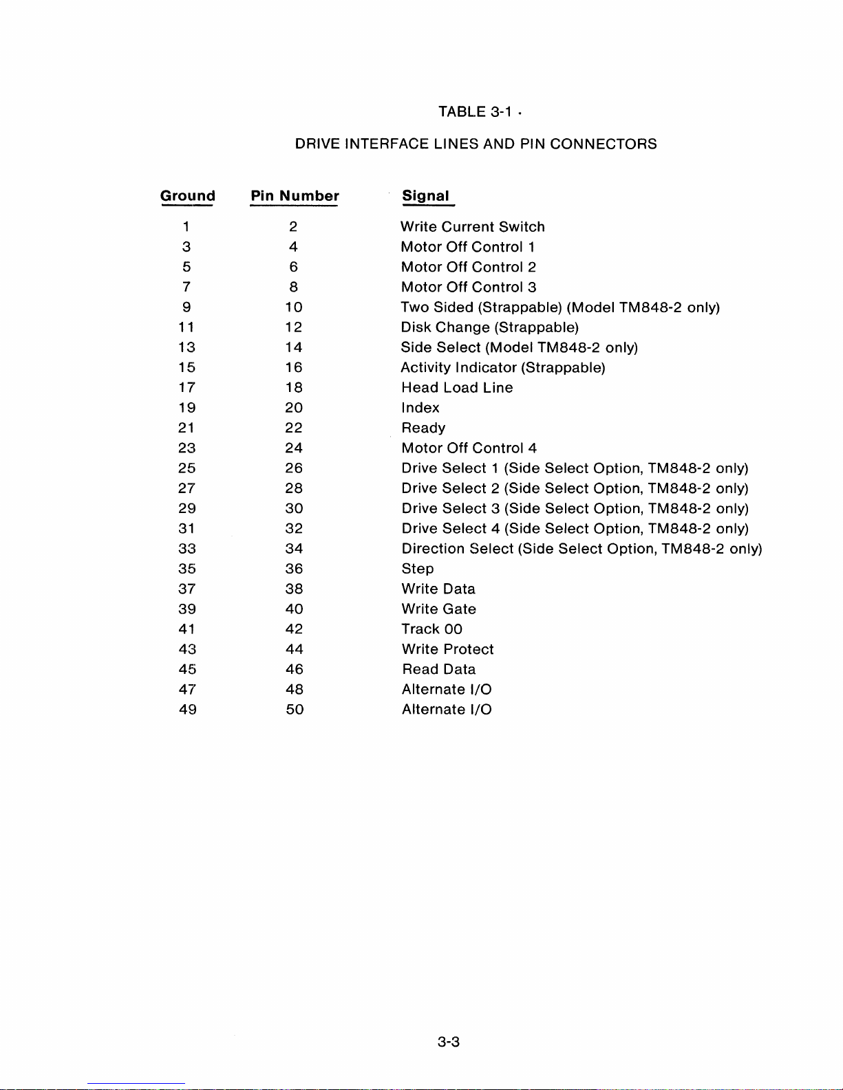
TABLE
3-1 .
DRIVE INTERFACE
LINES
AND
PIN
CONNECTORS
Ground
1
3
5
7
9
11
13
15
17
19
21
23
25
27
29
31
33
35
37
39
41
43
45
47
49
Pin
Number
2
4
6
8
10
12
14
16
18
20
22
24
26
28
30
32
34
36
38
40
42
44
46
48
50
Signal
Write
Current
Switch
Motor
Off
Control
1
Motor
Off
Control
2
Motor
Off
Control
3
Two
Sided
(Strappable)
(Model
TM848-2
only)
Disk
Change
(Strappable)
Side
Select
(Model
TM848-2
only)
Activity
Indicator
(Strappable)
Head
Load
Line
Index
Ready
Motor
Off
Control
4
Drive
Select1(Side
Select
Option,
TM848-2
only)
Drive
Select2(Side
Select
Option,
TM848-2
only)
Drive
Select3(Side
Select
Option,
TM848-2
only)
Drive
Select4(Side
Select
Option,
TM848-2
only)
Direction
Select
(Side
Select
Option,
TM848-2
only)
Step
Write
Data
Write
Gate
Track
00
Write
Protect
Read
Data
Alternate
I/O
Alternate
I/O
3-3

Functional
Description
The
TM848
has aD.C.
brushless
motor
that
can be
enabledinthree
ways:
1.
By
using
the
four
radial
Motor
Control
lines, MC1
through
MC4.
2.
By
the
Head
Load
line
using
shorting
plug M4. Using
this
line
enables
all drives'
Motor
On
lines.
3. By Drive Select, using
shorting
plug
M3.
The
MotorControllines,
MC1
through
MC4,
are
true
(low)
signals
that
turn
the
motor
off.
Shorting
plug
M2
must
be
installed
for
these
control
linestooperate.
WhenaMotor
Control
line is false (high),
the
drive
motor
acceleratestoits
operational
speed
in less
then
500
milliseconds. This
keeps
the
spindle
rotatingata
constant
speedof360
RPM.
When
the
Motor
Control
line is
true
(low)
the
motor
coaststoa stop.
When using
Head
Loadtoenable
the
drive motor,
M4
must
be installed. Allofthe
motors
are
enabled
when
the
Head
Load
line
goes
true
(low). M1
should
be installed if a
motor
turn
off
delay
is desired.
See
Section
1.19.21
foranadditional
descriptionofthis
circuit.
When a Drive
Select
lineistobeused
for
Motor
Enable,
M3
must
be installed. This
enables
the
drive
motor
when
the
Select
line
goes
low.
Circuit
Description
When
the
motorisenabledbyanyofthe
above, U35, Pin6,floats
high,
allowing
the
speed
control
U41
to
start
the
drive motor.
Two
Hall
Effect
transducersinthe
motor,
supply
the
necessary
feedback
signals
for
proper
speed
regulation.
When
U35-6
goes
high,
the
outputofU41, Pin6,turnson021,
whichinturn
applies
a varying
voltageto020
that
regulates
the
amountofcurrent
through
020,
and
the
motor
driver
transistors
01
through
04.
Transistors
01
through
04
are
turned
onbythe
gated
pulses
derivedfrom
the
conditioned
outputsofthe
Hall
Effect
transducers.The
conditioned
output
of
U38, Pin2, is
subsequently
conditionedbyGate
U36,
which
acts
asan
edge
trigger
and
pulse
doubler.
This signal is
fed
backtoU41, Pins 2
and3,which
resultsinclosed
loop
speed
control. The drive
motor's
rotational
speedisapproximately
2520
RPM,
when
adjusted,togiveaspindle
speedof360
RPM.
C.
DIR STEP,
Direction
and
Step
Lines
Functional
Description
When
the
drive is selected, a
true
(low)
pulse
withatime
duration
between
200
nanoseconds
and
2
millisecondsonthe
Step
line
initiates
the
track
access
motion. The
directionofmotionisdetermined
by
the
logic
stateofthe
Direction
line
whenaStep
pulse
is issued. The
motionistoward
the
center
of
the
driveifthe
Direction
line is in
the
true
(low)
state
whenaStep
pulse
is issued. The
direction
of
motionisaway
from
the
centerofthe
drive if
the
Direction
line is in
the
false (high)
state
whenaStep
pulse
is issued. To
ensure
proper
positioning,
the
Direction
line
shouldbestable
foraminimumof1
00
microseconds
before
the
trailing
edgeofthe
corresponding
Step
pulse. The
Direction
line
should
also remain
stable
until
100
microseconds
after
the
trailing
edgeofthe
Step
pulse. The
access
motionisinitiated
on
the
trailing
edgeofthe
Step
pulse.
When
the
carriageispositionedatTrack00and
the
stepper
motorisat
Phase0,
the
signalatPin42of
P13
goes
true
(low),
indicating
that
Track
00
has
been
reached.
When
steppinginor
out,
Test
Point
8 is a high
going
pulse
for
each
step
pulse
issued.
3-4

Circuit
Description
The
Direction
line
comes
in on Pin34of
the
interface
connector.
A high
signal
directs
the
step
logic
to
step
toward
Track
00. A
low
signal
directs
the
step
logictostep
towardahigher
numbered
track.
The
direction
line
sets
the
proper
phasetothe
exclusive
OR
gatesofU9.
TABLE 3-2
STEPPER LOGIC TRUTH TABLE
Step
Out
Toward
Track
00
Step
In Toward The
Upper
Tracks
Phase Phase
Pin No.
0
3 2 1
0
Pin No.
0
1
2
3 0
U21-9
0
1 1 0
0
U21-9
0
0
1 1
0
U21-B
1 0 0 1
1
U21-B
1
1
0 0
1
U21-5
0
0 1
1 0
U21-5
0
1
1
0
0
U21-6
1 1
0
0
1
U21-6
1
0
0
1 1
The
step
pulses
comeinat
Pin36of
the
interface
connector.
They
are
bufferedbyU22
and
gated
at
U14bythe
unit
select, and
the
Not
Write
signal.The
step
pulses
thengoto
theCinputsofthe
two
flip
flopsatU21.
The
directionofthe
step,
hence
the
selectionofthe
flip
floptobe
toggled,isdonebythe
two
exclusiveORgatesofU9.These
gates
are
controlledbythe
step
direction
line
andbythe
state
of
the
two
flip
flop
outputs.
The POR-
(Power
On
Reset) signal
resets
the
two
flip'
flopstoPhase 0
afteraPower
On.
The
outputofthe
twoflipflops
drives
the
stepper
motorthrough
the
driversofU39, U40,and U12.The
diodes, CR2-9, are
for
voltage
spike
elimination.
The
current
through
the
stepper
motor
coils
is
reversed
sequentially,
oneata time.
D.
WRf
GATE
Functional
Description
When
the
Write
Gate
signal is
true
(low),
the
write
electronics
are
prepared
for
writing
data
(read
electronics
disabled). This signal
turnsonthe
write
currentinthe
read/write
head. Data is
written
under
controlofthe
Write
Data
input
line.Itis
necessary
for
the
Write
Gate
interface
linetogo
low
before
the
first
Write
Data
pulse.
However,the
separation
between
the
leading
edgeofWrite
Gate
and
the
first
significant
Write
Data
pulse
should
notbeless
than
two
microseconds
and
not
greater
than
four
microseconds. The
same
restrictions
exist
for
the
relationship
between
the
last
Write
Data
pulse
and
the
terminationofthe
Write
Gate
signal. When
the
Write
Gate
line
goes
false (high),
the
trim erase will
stayonfor
550
microseconds
(see Trim Erase,
page
3-7).
When a
write-protected
diskette
is
installed
in
the
drive,
the
write
electronics
are disabled,
irrespectiveofthe
stateofthe
Write
Gate
line.
Check
the
listofoptions
(see
Section
1.19)
for
exceptions
and
further
discussionofwrite
protect
options.
Steppingisalso
disabledbya
true
(low)
Write
Gate.
Tandon
Corporation
recommends
that
the
controller
wait
one
millisecond
after
the
WRf
GATE
goes
high (false) be'fore
any
step
pulses
are
senttothe
drive.
Circuit
Description
A
low
(true) WRT GATE signal is
appliedtoPin
40ofthe
interface
connector
P13. This
signal
is
3-5

invertedand
gated
withWriteProtectand Drive
SelecttoenableU23, U30,and
013.
Transistors
013
and
012
are
write
current switches.
013
and
012
are on in parallel when
the
low Write
Current
interfaceis high (false). This results in awrite
currentof10
milliamps.When
the
low
WriteCurrentline
goes
low (true), transistor
012
turns
off, and
the
current decreasesto7 milliamps. R52 and
R51
determine
the
amount of
write
current suppliedtothe
head. The
network
CR1B, CR19, CR20,
RBO
and
RB1
is a power-loss
write
disable. If a sudden voltage loss occurs, transistor
014
turns
off,
disabling
the
write current.
E.
WRT DATA
Functional Description
When
the
driveisselected,
the
writedatalineprovides
the
bit-serialWrite Data pulses
that
control
the
switching of
the
write
current in
the
heads. The write electronics must be
conditioned
for writing by
the Write Gate line.
Foreach high-to-Iowtransitionon
the
WRTDATA line,afluxchangeis produced at
the
headwritegap.
This causes a flux change
tobestored on
the
diskette
(see Figure 3-4).
N INTERNAL WRITE BUSY SIDE
SELECT
LOGIC
SIDE
SELECT
NWRITE
DATA
NWRITE
GATE
N WRITE PROTECT
UNIT
SELECT
o a
WRITE
DATA
TRIGGER
C
WRITE
CURRENT
SOURCE
ERASE
DELAY
LOGIC
IN
WRITE)
WRITE
DRIVER
1
WRITE
DRIVER
2
ERASE
CURRENT
SOURCE
READ!
WRITE
COILS
ERASE
COIL
IN
INTERNAL
......
READ
DISABLE
~-------WRITE
BUSY)
Figure
3-4
Write Data Circuit Block Diagram
When a double-frequencytype encoding technique is used(in which data and
clock
form thecombined
Write Data signal),
it
is recommended
that
the
repetition of the high-to-Iow transitions, when writing
all zeros, be equal
to
the
nominal data rate ±0.1 percent. The repetition rate of the high-to-Iow
transitions, when writing all ones, should be equal
to
twice
the
nominal data rate
±O.1
percent. The
data transfer rate
for
a 1F pattern is
250,000
Bits Per Second (BPS). The data transfer rate
for
a 2F
pattern is
500,000
BPS.
3-6

Circuit
Description
Datais
senttothe
drivevia
interface
Pin 38. This signal is invertedbyU22, and is usedtoclock
the
D
flip
flop
U23. The
outputsofU23
are inverted subsequently,
and
usedtodrive
015
and
017,
which
direct
the
write
currenttothe
correct
winding.
F.
TRIM ERASE
Functional
Description
The
TM848
uses a
tunnel
erase
schemetoachieve
trim erase,
whichisusedtoerase a guard band
around
the
data
tracks, allowing
minor
track
offsets
and
minor
misalignment
without
data
errors
occurring.The erase
poles
are
staggered
.036
inch
behind
the
read/write
poles.At a mediarotational
speedof360
RPM,
the
tunnel
erase
method
requires
that
the
trim erase be
delayed
for
190
microseconds
afer
the
startofwriting
and
that
it be
continued
for
550
microseconds
after
the
end
of
writing
the
data. The
two
one
shotsinU30
provide
these
delay
time
intervals.
When
the
write
gate
goes
low, U30, Pin9,(A
input), is
triggered
and a hightolowtohigh
transition
of
190
us is generated. The
write
gate
is also appliedtoU30
Pin 1(Ainput).
When
the
write
data
is
appliedtothe
WRT DATA line,
U23
conditions
the
data
whichinturn
generates
the
signal WRT
TRAN+
(write
transition+).
This signal is
then
appliedtoU30
Pin2,(8
input)
which
is a positive
triggered
input.This
clock
will
retrigger
this
one
shot
continuously
until
the
last
transitionofthe
WRT
TRAN+
and WRT
GATE-
occurs.Atthis
time,
the
one
shot
stays on
foranadditional
550
us. These
outputs
(U30, Pins12and
13) are
gated
by U31
whichisthe
trime
erase gate. This
output
goes
low
whenever
both
inputs
are high,
causing
the
trim erasetobe
enabled
(see Figure 3-5).
G.
SIDE SELECT
Functional
Description
SIDE SELECTcan be
generated
three
ways.
See
the
option
listing,
Section
1.19,
for
this
information.
As
shipped
from
the
factory,
the
sideisselected
using
the
SIDE SELECT
interface
line.
When
the
Side
Select
signal is low,
Side
1 (the
upper
head)ofthe
drive is
selected
for
read/write
operations. When
this
signal is high,
Side
0 of
the
drive is
selected
(see Figure 3-6). The
Side
Select
signal must be
stable
duringanentire
readorwrite
operation. This signal is
best
implemented
in
synchronization
with
the
Drive
Select
line signal.
Circuit
Description
As
shipped
from
the
factory,
the
Side
Select
signal is received on Pin14of
edge
connector
P13. This
signal is received
by
U22, inverted,
then
inverted againbyU13.The
outputofU13, Pin 10,
generates
the
signal
called
Side
1-.
The
Side1-signal is
appliedtoU13, Pin9,and U24, Pin 13.The
outputofU13,Pin8,is
appliedtoU24,
Pin
1.
This
outputatPin 2ofU24isthe
oppositeofU24,
Pin12.
The
resistor
divider
network
sets
up
the
biasing
voltagestoturn
on and
turn
off
the
head
select
transistor,
018or019.
The head biasing
voltages
seen
across
the
collector
resistors will
be
5.2VD.C.
when
selecting
a head
for
a read
operation,
12V
D.C.
duringawrite
operation, andOVD.C.when
the
head is
not
selected. The
emitter
voltageson018
and
019
will alwaysbethe
oppositeofeach other,
causing
CTOorCT1
(center
tap
0,
center
tap1)tobeselected.
3-7

WRTGATE
WRT DATA
I
---J
~
I I
<1-
4usma<
550us
-i>1
I
_I
II.--
--[>
I I
<}-
190us
U
1<1-
_
__
Jr----------------I
U30, Pin 13 •
1.0,
------
Sec
B,
Q output
U30, Pin 12
Sec
A,
Q output
WRTTRAN +
U31, Pin3
Trim erase Source
Figure
3-5
Trim Erase Diagram

CTJ
51DE. \
POR.+
IN~
Wr.:.T
W::>Y-t:
~--4~cl)
I .
~\4
9~~
-----
~
~~e>-------!D~I~R'.:I+':
~4
+~v
-t-5V
+sv
ID
lif~.
5ii5E
14
5
-.
52.'0------
~14
".
0
5
\
150
11
+5V
. Figure 3-6
Side Select Schematic Diagram

3.4 OUTPUT
CONTROL
LINES
A.
INDEX/SECTOR
Functional
Description
The
Index
signal is provided
once
eash
revolution
(166.667
milliseconds
nominal)toindicate
the
beginningofa
tracktothe
controller.TheI
ndex
line remains in a
low
(true)
state
forthe
durationofthe
index
pulse.
The
durationofthe
Index
pulseisnominally
2.0 milliseconds.
Two
index
sensors
are
supplied
for
use
with
single-ordouble-sided
media.
The
leading
edgeofan
Index
pulse
is always used
for
timingtoensure
diskette
interchangeability
between
drives.
With a standard,
soft-sectored
diskette
installed,
the
signalatR33 (see
Figures
3-7
and
3-8) isa high
going
pulse,
nominally
2.0
milliseconds
in duration,
every
166.667
milliseconds.
Circuit
Description
Light
from
the
Index
L.E.D.
is usedtodrive
the
index
sensor,
whichisappliedtothe
inverting
input
of
U32. This signal is
conditioned
by
U32,
then
inverted
by
U33. It is
usedtodrive
U26. Then
the
Respective
index
pulses
are
gatedbyU20,
then
with
drive
selectbyU4togenerate
the
signal index.
U26
and
the
associated
support
integrated
circuitsU16
and
U20
are
configuredtoallow
only
the
Index
1 signaltobe
present
on
the
interface
whenatwo-hole
diskette
envelope
is used.
When a
double-sided
diskette
is installed,
the
signal IN1
FF+isgenerated
and
gatedbyU4toenable
the
output
TWO SIDED.
B.
Ready
Functional
Description
Ready is usedbythe
controllertoascertain
the
statusofthe
drive.This signal is
generated
when
the
drive
motor
is on,
the
diskette
installed,
and
the
drive is selected. The signal
takes
less than
700
millisecondstogo
true
(low) from a
motor
startbyDrive
SelectorHead
Load
(see
Section
1.19.21).
Circuit
Description
The
index
pulseisgatedbyU5,
which
in turn,
triggers
U17, a
220
millisecond
retriggerable
one
shot.
When
the
index-to-index
time
becomes
less than
220
milliseconds,
the
one
shot
becomes
continuously
enabled
and
generates
the
signal
SPIN-.
This signal is
gated
with
POR+,
Power
On
Reset,toenable
the
two-revolution
counters
U18. The
outputofU18, Pin8,enables
U6,
whose
outputisgated
with
Drive
Selecttogenerate
the
signal
ready.
Whenever
the
drive
motor
is disabled,
MTRON+
goes
low,
causing
this
sequence
to
be
repeated
when
the
motor
is restarted.
C.
Disk
Change
Functional
Description
The signal
DISK
CHANGEisusedtoindicate
the
host
controller
thatadisk
change
operation
has
been
made.
3-10

Circuit
Description
The
disk
change
flip-flop, U10,is resetbyOPEN-
whenever
the
lever
is in
the
open
position.
When
this
occurs, U
10-6
is high,
andatrue
disk
change
statusissenttothe
interfaceonPin12from U4-11.Flip-
flopU10issetonthe
trailing
edgeofdrive
select
causingU10-6togo
low
and
setting
the
disk
change
statustothe
false
state.
In
actual
use,
this
signal
can be
usedbythe
host
controllertodetermine
that
the
diskette
lever
has
been
opened
since
the
endofthe
previous
drive
select
operation.
r--'
I
~;f'--~ov
NOE')\.
\~~l{~9·
LED
"t.
1 1
7
(~
I i 'V
~..J.<iLJ~-~5V
''''OE'/..'Z.+"",I
~R~O-
LED
~
I~
I~
I:
'V
1 I
d:
~~~V
"\
I 1
:
I:,
Figure
3-7
Index
Schematic
Diagram
U
166.667ms
- - -
---a.t
Figure
3-8
WaveformatTest
Point11or
12
Alternate
Test
Point, R33
Soft
Sectored
Diskette
Installed
D.
TRK
00
Functional
Description
When
the
driveis selected,
the
Track00interface
signal
indicatestothe
controller
that
the
read/write
head is
positionedatTrack
00. The
Track00signal
remains
true
(low)
until
the
head is moved
away
from
Track
00. The
Track
00
sensorisactivated
internally
between
Tracks 2
and
3.
Interface
Pin42(see
Figure
3-9) is
true
(low)
when
the
carriageispositionedatTrack00and
the
step
motorisat
Phase
O.
3-11

P2.
r-,
Rt14
TR~CK
~~+5V
L~.O
~~
I I
\l
I I
TI1J).C~
C)>-i-':Z=-----.+5V
(1)
I I
~E.W50R..
I
II
I>i-'---..---+----~
L_.J
R1'5
I
Cc..c..
22K.Z.--lOOlpf
V V
pD
I I
221<.
RP3
RP2. 4701<.
U~I\'i
+SV
\PIO
.
I R.P4
2.
4:7K..
Figure
3-9
Track
00
Schematic
Diagram
Circuit
Description
When
the
read/write
carriageisrestoredtoTrack
00, a
tabonthe
carriage
blocks
light
from
the
Track
00
L.
E.
D.,
turning
off
the
Track00sensor
transistor.
This
enables
the
inverting
inputofU32, a
quad
comparator
causing
U32,
Pin 13,togo
high.
This
signalisgated
with
Phase0of
the
step
circuit
and
with
drive
selecttogenerate
the
signal
TRK
00.
The
signalatTest
Point10shouldgohigh
between
Tracks2and
3, as
the
carriageisbeing
moved
toward
TRK
00.
E.
WRITE PROTECT
Functional
Description
When
the
driveisselected
and
the
disketteiswrite
protected,
the
WRITE PROTECT
line's
true
(low).
The
write
electronics
are
internally
disabled
when
the
disketteiswrite
protected
(see
Option
Listing
for
exceptions).
When
the
signalonthe
WRITE PROTECT
lineisfalse
(high),
the
write
electronics
are
enabled
and
the
write
operation
canbeperformed.Itis
recommended
that
the
controller
not
issueaWrite
command
when
the
Write
Protect
signalistrue
(low).
It is
recommended
that
the
Write
Data
linebeinactive
whenever
Write
Gateisfalse
(high).
Circuit
Description
Whenawrite
protected
disketteisinstalled,
light
from
the
Write
Protect
L.
E.
D.isdetectedbythe
Write
Protected
sensor
transistor.
The
outputofthe
sensorishigh
andisconditioned
by
U32.
The
outputatPin
14islow
generating
the
signal
WR PROT-.
This
signalisused
internally
with
the
read/write
circuitry.
The
signal
WR PROT- is
invertedbyU33,
and
gated
with
DR
SEL+to
generate
the
Write
Protect
signal.
F.
READ DATA
Functional
Description
The
Read
Data
interface
line
transmits
the
read
datatothe
controller
when
the
driveisselected.
It
providesapulse
for
each
flux
transition
recordedonthe
media.
The
Read
Data
output
line
goes
true
(low)
foradurationof200
nanoseconds
for
each
flux
change
recorded.
The
leading
edgeofthe
low
going,
read
data
output
pulse
represents
the
true
positionsofthe
flux
transitions
on
the
diskette
surface.
3-12

tzt;
p~
~
WR\TE
_;
I I
150
PROTECT
,;v-
I I
L.E.D.
~
WRITE:
"'~)
:2.
+5V
PROTECT
: I
SENSOR
>;;-:-,
--
........
--.----
L_J
RPZ
7
22~
8
TP7
+5V
5
RP4
4.71(,
Figure
3-10
Write
Protect
Schematic
Diagram
Test
Points2and
3 (see
Figure
3-11)
are
providedtoobserve
the
differential
outputofthe
first
stage
of
Read
signal
preamplification.
Test
Points4and
5 are
providedtoobserve
the
differential
output
of
the
second
stage
amplifier
and
differentiated
Read signal.
Test
Point
9 is
the
outputofthesingle
shot
used in
the
Read section,
nominally
200
nanoseconds
for
each
flux
transition
detected.
Test
Point
1
is signal ground.
Circuit
Description
The read signal
comes
from
the
selected
head on
the
drive.Itis
gatedtothe
preamplifier
U7bythe
-Write
signaltoU25,
which
forward
biases
diodes
CR14
and
CR15. Then,
the
Read signal passes
throughalinear
bandpass
filter. The Read signal is
then
inputtoU2,
the
differentiator.
The
outputofU2
goes
through
theD.C.
blocking
capacitorstothe
crossover
detector,
U8,
which
digitizes
the
signal. This
converts
the
signal
into
standard
TIL
level I
ntegrated
circuits
U9, U11,
and
U10
compriseacomparator
circuit.
Any
pulses
that
occur
outsideofthe
normal
duty
cycleofU11are
eliminated. U9 is an
edge
detector.
U11
acts
as a
one
shot,
withatimeoutofapproximately
860
nanoseconds.U10 is
the
actual
comparator.
The Read signal is
presentedtoU9. Then it
goestoU11,
where
the
pulses
are
shapedto200
nanoseconds.This
outputisgatedatU29
with
the
Unit
Select
signaltoproduceadigital
outputatPin
46ofthe
interface
connector
(see
Figure
3-12).
Note
U11,
the
final
one
shot, is
disabled
when
the
drive is
writing
data
onto
the
diskette.
G.
Two
Sided
Functional
Description
This
output
enables
the
controllertodetermine
if a
diskette
is installed,
which
utilizes
the
Index
2
index
hole.This maybe usedtoindicatetothe
host
controller
thatatwo-sided
diskette
is in
the
drive.
3-13

T POINT 3
TEST POINT 2
....
T
UPPER
...
HEAD
...
......
....
---..
I
READ AND HEAD
SIGNAL
SWITCHING
AMPLIFIER
~TES
...
CIRCUITS
....
LOWER
~
......
HEAD
...
TEST POINT 4
,
~
l+
.....
CROSSOVER
....
TIME DOMAIN
DIFFERENTIATOR
,
....
DETECTOR
r
FILTER
.....
.....
.....
TEST POINT 5
~
....
DIGITIZER
.....
DATA OUTPUT
NT
WAT BUSY
-f
,.4~
UNIT SELECT _
Figure
3-11
Read
Circuit
Block
Diagram
Circuit
Description
When a
two-sided
diskette
is installed,
the
signal IN1
FF+isgenerated
and
gatedbyU4toenable
the
low-going
output
Two
Sided. The IN1 FF signal also
goestothe
ready
circuitryatU6-5todisable
Ready in
the
event
that
the
upper
head (Head 1) is
selected
whenasingle-sided
(Head0)diskette
is
installed (see
Option
RM
for
further
discussion).
3-14

Figure
3-1~Diagram
t
Schematic
Read Da a

SECTION
IV
TROUBLESHOOTING
GUIDE
4.
INTRODUCTION
This
sectionispresentedinthe
formofa table.
Each
section
contains
four
major
parts:
1.
The
section
number.
2. A
statementofthe
presenting
condition.
3. A
listofthe
possible
causesofthe
condition.
4.
The
recommended
actiontobe
taken.
4-1

SECTION
4.1
CONDITION
NOT READY
AND/OR
NO INDEX
POSSIBLE CAUSE
Diskette
not
inserted.
Diskette
not
clamped.
Unit
not
selected.
Drive
motor
not
turning
I
ndex
sensor
not
connected.
Index
sensor
defective.
RECOMMENDED ACTION
Insert
diskette.
Turn
knob
lock
lever
clockwisesothat
it
is
perpendicular
to
the
diskette
insertion
slot.
Verify
unit
select
and
jumper
configuration.
Verify
interface
drive
motor
on.
Check
Connector
P6.
Verify drive
belt
installed
Replace
circuit
board.
Replace Drive
Motor
Assembly.
Check
P1.
Replace
index
sensor.
4.2
WILL
NOT SEEK
OR RESTORE
Interface
not
enabled. Verify
interface
direction,
step, and
select
signals.
Step
motor
disconnected.
Check
Connectors
P4 and P5.
Defective
step
logic.
Defective
stepper
motor.
Wrong
option
selected.
4-2
Replace
circuit
board.
Replace
Stepper
Motor
Assembly.
Check
options
OS
and HL
for
the
particular
application.

SECTION
CONDITION
POSSIBLE CAUSE
RECOMMENDED
ACTION
-----
4.3
WILL
NOT WRITE
I
nterface
not
enabled.
Verify
write
enable, select,
and
write
data
interface
lines.
Headsorwrite
protect
switch
not
connected.
Check
Connectors
P3, P8,
and
P9.
Write
protect
switch
misadjusted.
Check
write
protect
switch
operation.
Defective
write
logic.
Replace
circuit
board.
Defective
heads.
Replace
Head
Carriage
Assembly.
Misadjusted
platen
Adjust
platen
load arm.
load arm.
4.4
WILL
NOT READ
Interface
incorrect.
Verify
selectistrue
and
write
enable
is false.
Alignment
off.
Verify
C.E.lobes,
index
burst,
and
Track00sensor
adjustment.
Defective
read
Replace
circuit
electronics.
board.
Defective
heads.
Replace
Head
Carriage
Assembly.
Platen load arm
misadjusted.
Adjust
platen
load arm.
4.5
ACTIVITY
L.E.D.
INOPERATIVE
I
nterface
not
enabled.
4-3
Verify
interface
select
and
jumper
configuration.

SECTION
CONDITION
POSSIBLE CAUSE
RECOMMENDED
ACTION
4.5 ACTIVITY
L.E.D.
INOPERATIVE
Activity
L.E.D.
Check
P11
not
connected.
Activity
L.E.D. Replace
Activity
defective.
L.E.D.
Assembly.
Activity
L.E.D. Replace
circuit
driver
defective.
board.
4.6
NO TRACK
00
SENSOR
INDICATION
Defective
seek.
See
Section
4.2
4.7
Track
00
sensor
not
connected.
Defective
logic.
Defective
Track
00
sensor.
DRIVE MOTOR
WILL
NOT START
WHEN DOOR
LATCHED.
Defective
microswitch.
M
icroswitch
not
connected.
Misadjusted
switch
bracket.
4-4
Check
P2.
Replace
circuit
board.
Replace TrackOO
Sensor
Assembly.
Replace switch.
Check
P14.
Realign.

SECTION
V
REPLACEMENT
PROCEDURES
5
INTRODUCTION
This
section
contains
the
replacement
procedures
for
the
TM848
familyofdisk
drives'
parts
and
assemblies:
'1.
0 rive
Belt
2.
Drive
Motor
~3.
Circuit
Board
4.
Cone
Assembly
!5.
Diskette
Lever
6.
Bridge
Assembly
7.
Front
Panel
8.
Activity
L.E.D.
9.
Load
Arm
Assembly
10.
Track00Sensor
Assembly
1
"I.
Write
Protect
Sensor
Assembly
12.
Door
Switch
Assembly
1
~3.
Index
Sensor
Assembly
14.
Diskette
Ejector
Assembly
1
t5.
Load
Resistor
Assembly
16.
Stepper
Band
17.
Stepper
Motor
Assembly
18.
Head
Carriage
Assembly
5.1
DRIVE
BELT
5.1.1 Removal
A.
Turn
the
drive
oversothat
the
spindleisfacing
upward
(see
Figure
5-1).
5-1

DRIVE BELT
o
SMALL
FLANGED
SPINDLE
PULLEY
o
c==>
J
o
LARGE
SPINDLE
PULLEY
Figure
5-1
Drive
Belt
and
Spindle
B.
Grasp
the
drive belt,
and
remove it from
the
pulleys.
5.1.2
Installation
A.
With
the
shiny
side
inward,
loop
the
new
drive
belt
onto
the
small,
flanged
spindle
pulley.
B.
While
turning
the
spindle,
put
the
drive
beltonthe
large
spindle
pulley.
5.1.3
Checks
A.
After
turning
the
drive
motor
on,
check
that
the
drive
belt
does
not
sliporfall off
the
large
pulley.
B.
Check
the
spindle
speed
(see
Section
II).
5.2 DRIVE MOTOR
5.2.1 Removal
A.
Remove
the
drive
belt
(see
Section
5.1).
B.
After
turning
the
driveover,
cut
the
tie
wraps
that
hold
the
drive
motor's
wires
(see Figure5-2).
C.
Unplug
P6 from
the
circuit
board.
D.
Remove
the
three
mounting
screws
that
attached
the
drive
motor
tothe
chassis.
E.
Lift
out
the
drive motor.
5.2.2
Installation
A.
Set
the
drive
motoronthe
chassis,
aligning
the
three
mounting
holes.
B.
Reinstall and
tighten
the
three
mounting
screws.
5-2

DRIVE
MOTOR
DRIVE MOTOR WIRES
P6
Figure 5-2
Drive
Motor
and
Related Parts
C.
Carefully
rebundle
the
wires,
including
the
drive
motor
wire,
and
cable
harness
them
(see
Figure
5-2).
D.
Plug P6
into
the
circuit
board.
E.
Turn
the
drive over, and reinstall
the
drive
belt
(see
Section
5.1.2).
5.2.3
Checks
A.
Checktoensure
that
the
drive
motor
works.
B.
Check
the
spindle
speed
(see
Section
II).
5.3 CIRCUIT BOARD
5.3.1 Removal
A.
Remove all
the
connectors
from
the
circuit
board.
B.
Remove
the
two
side
mounting
screws
that
connect
the
two
regulator
heat
sinkstothe
drive's
chassis (see
Figure
5-3).
C.
Remove
the
screw
and
the
retaining
clip
that
attach
the
circuit
boardtothe
dirve's chassis.
D.
Lift
the
circuit
board
away
from
the
drive.
E Remove
the
power
connector
by
pushing
down
on its top.
Lift
its
wires
out, using
the
slot
provided (see
Figure
5-3).
5.3.2
Installation
A.
Install
the
power
connector
by
rethreading
the
power
wires
and
pushinginthe
power
connector
from
the
backofthe
drive.
5-3

RETAINING CLIP'
---=--_~
Figure
5-3
Circuit
Board
Mounting
Screws
B.
Remount
the
circuit board using
the
two
screwstothe
two
heat
sinks
and
the
screw
and
nylon
clip
that
attach
the
circuit
boardtothe
drive's chassis.
C.
Plug in all
connectors,
ensuring
that
each
oneisseated
correctly
in its
proper
location.
5.3.3
Checks
A.
Verify
the
select
and
options
configuration.
B.
Applying power,
check
the
operationofthe
drive.
5.4
CONE
ASSEMBLY
5.4.1 Removal
A.
Remove
the
screw
that
attaches
the
cone
brackettothe
cone
alignment
arm (see Figure 5-4).
B.
Unlatch
the
diskette
lever.
C.
Swing
the
Cone
Assemblyup90
degreessothatitpoints
toward
the
sideofthe
drive.
D.
Carefully
remove
the
E-Ring, flat washer,
and
washer
that
holdsonthe
cone
shaft.
E.
Gently
lift
out
the
Cone
Assembly.
5.4.2
Installation
A.
Gently
insert
the
Cone
Assembly.
B.
Carefully
insert
the
E-Ring, flat washer, and wave
washer
that
holdsonthe
cone
shaft
(see
Figure
5-5).
C.
Swing
the
Cone
Assembly
down90degreessothatitpoints
toward
the
bottomofthe
unit.
5-4

CONE BRACKET
SCREW
CONE
ALIGNMENT
ARM
CONE ASSY
Figure
5-4
Cone
Assembly
Key
Parts
D.
Latch
the
diskette
lever.
! E-RING &WASHER
WAVE WASHER
E.
I
nsert
the
screw
that
attaches
the
cone
brackettothe
cone
alignment
arm(see
Figure
5-5).
t
E-RING
~
~-~-------
~i=c::::::l""""------
FLAT WASHER
~i~""""
WAVE WASHER
I:~f?:t"tj:@~
?]f!M,j~A~tfrJ!
.....
o1(f------
CONE
BRACKET
FLAT WASHER (2)
Figure
5-5
Cone
Assembly
Parts
5.4.3
Checks
A.
Ensure
that
the
Cone
Assembly
turns
freely.
B.
If not, reverify
that
the
Cone
Assembly
has
been
installed correctly.
C.Insertadiskette.
D.
Ensure
that
the
disketteisclamped
properlybythe
cone.
5-5

5.5 DISKETTE LEVER
5.5.1 Removal
A.
Pry
off
the
cover
that
hides
the
diskette
lever's retaining
screw
(see
Figure
5-6).
MOUNTING
SCREW
~"
COVER
DISKETTE LEVER
Figure
5-6
Diskette
Lever
Key
Parts
B.
Remove
the
diskette
lever's
retaining
screw.
C.
Carefully
remove
the
diskette
lever.
5.5.2
Installation
A.
Put
the
diskette
leveronthe
shaft.
B.
Put a
dropofLocktite
Number
234
on
the
threadsofthe
diskette
lever's screw.
C.
Install
and
tighten
the
diskette
lever's screw.
D.
Put
the
cover
backonthe
diskette
lever.
5.5.3
Checks
A.
Ensure
that
the
diskette
leverisperpendiculartothe
drive
when
the
diskette
isclamped.
See
Figure 5-7
for
the
adjustment.
.B.Ensure
that
the
diskette
lever
is paralleltothe
drive
when
the
diskette
is unclampled.
See
Figure 5-7
for
the
adjustment. -
5.6 BRIDGE
ASSEMBLY
5.6.1 Removal
A.
Remove
the
circuit
board (see
Section
5.3.1).
B.
Remove
the
diskette
lever
(see
Section
5.5.1).
C.
Remove
the
four
bridge
mounting
screws
that
attach
the
Bridge
Assemblytothe
chassis
(see)
Figur
5-8).
5-6

BEZEL
SCREWS
2 BOTH SIDES
Figure
5-7
Diskette
Lever
Adjustment
BRIDGE
MOUNTING
SCREWS
2 BOTH SIDES
I
•
I
~
Figure
5-8
Bridge
Assembly
Key
Parts
BEZEL
~
DISKETTE LEVER
'---
BEZEL
MOUNTNG SCREWS, 2
@
D.
Carefully
pull
out
the
two
indexL.E.
D.'s in
the
Bridge
Assembly.
E.
Carefully
lift
out
the
Bridge
Assembly
toward
the
backofthe
drive. The
shaft
must
clear
the
bezel.
5.6.2
Installation
A.
Insert
the
shaft
into
the
bezel
and
lay
the
Bridge
Assembly
in place.
B.
Install
and
tighten
the
four
bridge
mounting
screws
that
attach
the
Bridge
Assemblytothe
chassis.
C.
Install
the
two
index
L.E.D.'s
into
the
Brid.ge Assembly.
D.
Install
the
diskette
lever
(see
Section
5.5.2).
E.
Install
the
circuit
board
(see
Section
5.3.2).
5.6.3
Checks
A.
Ensure
that
the
diskette
lever
clamps
the
cone
and
loads
the
head (see Figure 5-9).
5-7

.....--------1
MOUNTING SCREWS (2 EA SIDE)
FigureS-9
~
Bridge
Assembly
Additional
Key
Parts
5.7
BEZEL
5.7.1 Removal
A.
Remove
the
diskette
lever
(see
Section
5.5).
SHAFT
MOUNTING
SCREWS
(2EASIDE)
B.
Remove
the
four
bezel
mounting
screws,
two
on
each
side,
that
attach
the
bezeltothe
chassis
(see
Figure
5-10).
~
DISKETTE LEVER
BEZEL
MOUNTING SCREWS, 2
Figure
5-10
Bezel
and
Related
Parts
C.
Lift
off
the
bezel,
being
careful
that
the
Activity
L.
E.
D.
comes
outofits
mounting
with
no
binding.
5-8

5.7.2
Installation
A.
Put
the
bezelonthe
drive,
ensuring
that
the
Activity
L.
E.
D.
goes
into
its
holder.
B.
Install
the
four
bezel
mounting
screws
that
attach
the
bezeltothe
chassis.
5.7.3
Checks
A.
Ensure
that
the
Activity
L.
E.
D.
goes
on
when
required.
B.
Ensure
that
the
diskette
lever
clamps
the
cone
and
loads
the
head.
5.8 ACTIVITY
L.
E.
D.
5.8.1 Removal
A.
Remove
the
bezel
(see
Section
5.7.1).
ACTIVITY
LED.
(INSIDE)
ACTIVITY LIGHT WIRES
BRACKET
1 NEAR SIDE
TIE BRACKETS
2 FAR SIDE
J 0
o~
o 0
B.
Remove
the
brackets
that
hold
the
bundleofwires
goingtoP11 from
the
chassis
(see
Figure
5-11
).
Figure
5-11
Activity
L.
E.
D.
Key
Parts
C.
Remove
the
Activity
L.
E.
D.
and
its
wires
after
unplugging
P11.
5.8.2
Installation
A.
Install
the
Activity
L.
E.
D.
into
the
bezel.
B.Install
the
bezel.
C.
Attach
the
Activity
L.
E.
D.
wirestothe
chassis
with
brackets
(see
Figure
5-11).
D.
Plug P11
into
the
circuit
board.
5.8.3
Checks
A.
Ensure
that
the
Activity
L.
E.
D.
does
not
interfere
with
the
drive
mechanisms.
B.
Ensure
that
the
Activity
L.
E.
D.
goesonwhen
required.
5-9

5.9 LOAD
ARM
ASSEMBLY
5.9.1 Removal
A.
Remove
the
circuit
board
(see
Section
5.3.1).
B.
Remove
the
mounting
screw
and
washer
that
are
usedtoattach
the
Load
Arm
Assembly
to
the
chassis
(see
Figure
5-12).
LOAD ARM
....
REAR
MOUNTING
SCREW, WASHER, AND SPRING
Figure
5-12
Load
Arm
Assembly
Key
Parts
C.
Carefully
slide
out
the
Load
Arm
Assembly
toward
the
rearofthe
chassis.
5.9.2
Installation
A.
Slide
the
Load
Arm
Assembly
into
position
from
the
rearofthe
chassis,
ensuring
that
the
load
springissitting
under
the
front of
the
mounting
screw.
B.
Install
and
tighten
the
mounting
screw
that
attaches
the
Load
Arm
Assemblytothe
chassis,
ensuring
that
the
washerisunder
the
screw
and
that
the
head
lift
armisover
the
Load
Arm
Assembly.
C.
Install
the
circuit
board
(see
Section
5.3.2).
5.9.3
Checks
A.
Insertadisketteinthe
drive.
B.
Ensure
that
the
headisloaded
when
the
diskette
leverisactivated
and
that adequate
clearanceisattained
for
diskette
insertion
and
ejection
(see
Section
II).
5.10
TRACK
00
SENSOR
ASSEMBLY
5.10.1
Removal
A.
Remove
P2
from
the
circuit
board.
B.
Cut
the
tie
wraps
that
hold
the
cable
harness,
and
remove
the
P2
wires
(see
Figure
5-13).
5-10

o
TRACK
00
SENSOR
ASSEMBLY
BFIACKET
-++-t---:;;~~~
Figure
5-13
Track00Sensor
Assembly
Key
Parts
C.
Remove
the
P2
wires
from
the
bracket
attachedtothe
chassis.
D.
Remove
the
two
mounting
screws
that
hold
down
the
Track
00
Sensor
Assembly.
E.
Lift
off
the
Track00Sensor
Assembly.
5.10.2
Installation
A.
Using
the
two
original
mounting
screws, install
the
Track00Sensor
Assembly.
B.
Loop
the
P2
wires
from
the
Track00Sensor
Assembly
through
the
bracket
attachedtothe
chassis.
C.
Using
tie
wraps,
cable
harness
the
P2
wires
and
the
other
wires
together.
D.
Plug P2
into
the
circuit
board.
5.10.3
Checks
A.
Adjust
the
Track00sensor
(see
Section
II).
5.11
5.11.1
WRITE PROTECT
SENSOR
ASSEMBLY
Removal
A.
Remove P3 from
the
circuit
board.
B.
Remove
the
two
mounting
screws
that
attach
the
Write
Protect
Sensor
Assemblytothe
chassis
(see
Figure
5-14).
C.
Cut
the
tie
wraps
that
hold
the
wirestothe
cable
harness,
and
lift
out
the
Write
Protect
Sensor
Assembly.
5-11

MOUNTING
SCREWS (2) .
P3
WRITE PROTECT
SENSOR
ASSY.
Figure
5-14
Write
Protect
Sensor
Assembly
Key Parts
5.11.2
Installation
A.
Using
the
two
original
mounting
screws,
attach
the
Write
Protect
Sensor
Assemblytothe
chassis.
B.
Plug P3
into
the
circuit
board.
C.
Tie
wrap
the
Write
Protect
wirestothe
cable
harness.
5.11.3
Checks
A.
Verify
operationofthe
Write
Protect
Sensor
Assembly.
5.12
5.12.1
DOOR SWITCH
ASSEMBLY
Removal
A.
Remove
P14
from
the
circuit
board.
B.
Remove
the
mounting
screw
from
the
door
switch
bracket
(see Figure 5-15).
C.
Cut
the
tie
wraps
leadingtoP14.
D.
Lift
out
the
Door
Switch
Assembly.
5.12.2
Installation
A.
Mount
the
Door
Switch
Assemblytothe
bridge, using
the
original
mounting
screw.
B.
Plug
P14
into
the
circuit
board.
5.12.3
Checks
A.
Ensure
that
the
door
switch
operates
properly.
5-12

5.13 INDEX
SENSOR
ASSEMBLY
MOUNTING
SCREW
P14
DOOR SWITCH
ASSEMBLY
Figure
5-15
Door
Switch
Assembly
Key
Parts
5.13.1
Removal
A.
Remove
the
circuit
board
(see
Section
5.3.1).
B.
Gently
remove
the
two
index
L.E.D.
's from
the
Bridge
Assembly
(see
Figure
5-16).
P1
UPPER INDEX
SENSORS
TIE WRAPS
Figure
5-16
Index
Sensor
Assembly
Key
Parts,
Top
View
c.
Turn
the
drive
over
and remove
the
mounting
screw
from
the
Index
Sensor
Assembly
(see
Figure
5-17).
D.
Remove
the
two
brackets
that
attach
theIndex
Sensor
Assembly's
wirestothe
chassis
(see
Figure
5-16).
5-13

E.
Cut
the
tie
wraps
along
the
cable
harness
(see
Figure
5-16).
F.
Lift
out
theIndex
Sensor
Assembly
(P1).
TIE BRACKETS, 2 FAR SIDE
TIE BRACKET. 1 NEAR SIDE
MOUNTING
SCREW
o
J
o
o
0
Figure
5-17
Index
Sensor
Assembly
Key
Parts,
Bottom
View
5.13.2
Installation
A.
Put
the
Index
Sensor
Assembly
into
the
drive.
B.
Loop
the
wirestothe
cable
harness
and
chassis.
C.Insert
the
two
L.E.D.
index
sensors
into
their
sockets.
D.
Using
the
original
mounting
screw,
attach
the
index
L.E.D.tothe
drive's
chassis.
E.
Cable
harness
the
bundleofwires,
including
theIndex
Sensor
Assembly's
wires.
F.
Reinstall
the
circuit
board
(see
Section
5.3.2).
5.13.3
Checks
A.
Check
the
index-to-data
adjustment
(see
Section
II).
5.14
DISKETTE EJECTOR
ASSEMBLY
5.14.1 Removal
A.
Remove
the
circuit
board
(see
Section
5.3.1).
B.
Remove
the
door
lock
lever
(see
Figure
5-6).
C.
Locate
and
remove
the
four
screws,
two
on
each
side,
that
hold
the
Bridge
Assembly
(see
Figure
5-7).
5-14

EJECTOR SPRING
TRIGGER
ASSEMBLY
Figure
5-18
Diskette
Ejector
Assembly
Key
Parts
D.
Lift
up
the
Bridge
Assembly
approximately
two
inches,
taking
care
nottopull
the
L.
E.
D.'s
from
their
sockets.
E.
Release
the
spring
attachedtothe
rearofthe
ejector.
F.
Remove
the
ejector.
5.14.2
Installation
A.Insert
the
ejector.
B.
Engage
the
spring
attachedtothe
rearofthe
ejector.
C.Insert
the
Bridge
Assembly
approximately
two
inches,
taking
caretoput
the
L.
E.
D.'sin
their
respective
sockets.
D.
Reinstall
the
original
four
screws
that
hold
the
Bridge
Assembly.
E.
Push on
the
lever.
Reinstall
the
retaining
screw.
Insert
the
small
pluginthe
door
lever.
F.
Reinstall
the
circuit
board
(see
Section
5.3.1).
5.14.3
Checks
A.Insertawork
diskette
into
the
drive.
B.
Ensure
that
the
diskette
staysinpriortobeing
closed.
C.
Close
and
open
the
diskette
lever.
D.
The
diskette
should
eject.
E.
If
not,
see
Section
5.4.
5.15 LOAD RESISTOR
ASSEMBLY
5-15

5.15.1 Removal
A.
Remove
P5
from
the
circuit
board.
B.
Remove
the
circuit
board
(see
Section
5.3.1).
C.
Remove
the
two
mounting
screws
that
attach
the
Load
Resistor
Assemblytothe
chassis.
D.
Unsolder
the
wirestothe
load
resistors
(see
Figure
5-19).
E.
Markoridentify
these
wiressothat
they
can
be
put
backinthe
same
location.
SOLDER JOINT, 4 PLACES
LOAD RESISTOR ASSEMBLY·
Figure
5-19
Load
Resistor
Assembly
and
Key
Parts
5.15.2
Installation
A.
Solder
the
wires
backinthe
same
placeatwhich
they
were
originally.
B.
Mount
the
Load
Resistor
Assembly
onto
the
chassis
using
the
two
original
mounting
screws.
C.
Install
the
circuit
board
(see
Section
5.3.2).
D.
Plug P5
into
the
circuit
board.
5.15.3
Checks
A.
Enable
the
drive
through
the
interface
logic.
B.
Step
the
drivetoTrack
00.
C.
Step
the
drivetoTrack
76.
D.
Do
the
C.E.alignment
verification
procedure
(see
Section
II).
5-16

5.16
5.16.1
STEPPER
BAND
Removal
It
is
suggested
that
the
drivebereturnedtoan
authorized
Tandon
repair
center
when
removing
the
stepper
band.
A.
Remove
the
circuit
board
(see
Section
5.3.1).
B.
Lift
off
the
stepper
band
from
the
spring
tensioner
(see
Figure
5-20).
SCREW, ATTACHES BANDTOCARRIAGE
ASSEMBLY
SPRING
TENSIONER
Figure
5-20
Stepper
Band
Key
Parts
C.
Remove
the
screw
that
attaches
the
frontofthe
stepper
bandtothe
Head
Carriage
Assembly.
D.
Remove
the
mounting
screw
that
attaches
the
stepper
bandtothe
stepper
pulley.
E.
Lift
out
the
stepper
band.
5.16.2
Installation
A.
Screw
the
frontofthe
stepper
band'into
the
Head
Carriage
Assembly
(see
Figure
5-21).
B.
Loop
the
stepper
band
around
the
stepper
pulley.
C.
Attach
the
rearofthe
bandtothe
spring
tensioner.
D.
Attach
the
stepper
bandtothe
stepper
pulley
loosely
with
the
mounting
screw.
E.
Move
the
Head
Carriage
Assembly
back
and
fourthatleast
five times.
F.
Visually
inspect
the
stepper
bandtoensure
that
it is
centered
on
the
stepper
pulley.
G.
Tighten
the
mounting
screw
that
attaches
the
stepper
pulleytothe
stepper
band.
H.
Install
the
circuit
board
(see
Section
5.3.2).
5.16.3
Checks
A.
Check
the
C.E.alignment
(see
Section
II).
5-17

STEPPER MOTOR
ASSEMBLY
o
MOUNTING
SCREWS, 3 PLACES
5.17
5.17.1
Figure
5-21
Stepper
Band
Additional
Key
Parts
STEPPER
MOTOR
ASSEMBLY
Removal
It is
suggested
that
the
drivebereturnedtoan
authorized
Tandon
repair
center
when
removing
the
Stepper
Motor
Assembly.
A.
Remove
the
circuit
board
(see
Section
5.3.1).
B.
Remove
the
stepper
band
(see
Section
5.16.1).
C.
Remove
the
three
mounting
screws
that
attach
the
Stepper
Motor
Assemblytothe
chassis
(see
Figure
5-22).
D.
Remove
plug
connectors
P4
and
P5
from
the
circuit
board.
E.
Cut
the
tie
wraps
that
connect
the
stepper
motor
wirestothe
load resistors.
F.
Lift
out
the
Stepper
Motor
Assembly.
Note
Be
careful
nottodamage
the
stepper
band.
5.17.2
Installation
A.
Place
the
Stepper
Motor
Assembly
into
the
drive's
chassis.
B.
Using
the
original
three
mounting
screws,
attach
the
Stepper
Motor
Assemblytothe
chassis.
5-18

STEPPER MOTOR
ASSEMBLY
o
MOUNTING
SCREWS, 3 PLACES
Figure
5-22
Stepper
Motor
Assembly
Key
Parts
C.
Replace
the
stepper
band
(see
Section
5.16.2).
D.
Replace
the
circuit
board
(see
Section
5.3.2).
5.17.3
Checks
A.
Align
the
C.E.lobesonthe
drive
(see
Section
II).
5.18
5.18.1
HEAD CARRIAGE
ASSEMBLY
Removal
It is
suogested
that
the
drivebereturnedtoan
authorized
Tandon
repair
center
when
removing
the
Head
Carriage
Assembly.
A.
Remove
the
Stepper
Motor
Assembly
(see
Section
5.17.1).
B.
Remove
plug
connectors
P8
and
P9
from
the
circuit
board.
C.
Cut
the
tie
wraps
that
hold
the
head
cablestothe
chassis.
D.
Remove
the
clip
that
holds
the
head
cablestothe
head
cable
flexure
bracket.
E.
Remove
the
four
mounting
screws
that
attach
the
carriage
shafttothe
chassis
(see
Figure
5-
23).
5-19

MOUNTING
SCREWS
4 PLACES
Figure
5-23
Head
Carriage
Removal
F.
Lift
out
the
Head
Carriage
Assembly.
5.18.2
Installation
A.Install
the
carriage
shaftinthe
carriage.
B.
Using
the
four
original
mounting
screws,
attach
the
carriage
shafttothe
chassis.
C.Install
the
Stepper
Motor
Assembly
(see
Section
5.17.2).
Note
Take
care
nottodamage
the
Arm
Spring
Assembly.
D.
Plug
connectors
P8
and
pg
into
the
circuit
board.
E.
Cable
harness
the
Head
Carriage
Assembly's
wirestothe
main
wire
bundle.
5.18.3
Checks
A.
Check
the
azimuth
(see
Section
II).
B.
Check
the
Cats
Eye
alignment
(see
Section
II).
C.
Check
the
index
alignment
(see
Section
II).
5-20

APPENDIX
I
PRINTED
CIRCUIT
BOARD
SCHEMATICS
AND
ASSEMBLY
DRAWINGS

B
o
c
1
I
I
I
I
I
~
ItEVISIONS
DESCItIPTION
~WCE
DE5\C:IN~Tl~
LA~T
U:;EO
U4'
ILS I
C"2.
I
QZ'
ICR~\
I RI43 I
APPllCMIlE
P.C.MNtO
RW.lE\fl:l
Ztoo<oo-ooD
REV-I>-
~~"(
REV
·If.VEL
Z10034-DOO
REV.G-J
2
SlGNATUIlES
~TE
'."dan
(H[
COllftORATtOII
A
IllS
MODEL
B4B
.-
Dl5K..£TTE
DR\VE
ELEcrR~\e5.
Ml'lL:
!CALI
2
REV
+24v--4-m:
I I
H8NJ
I I LOA.O
I I
~LaJOtD
I I
,I
I
R9f.. I I
L_.J
FlIO
I~
12.
01_ININCHES
1UaNCIS:
JOe :I:01AHCIAM
JOOC
:I:
DOS
:I:
lIZ'
~:I:
.;
_ALL_a:.es
-".0'0
FINISH:
'htI'~
...
TlOatOllTAJ~~
..
T"_
PItOPC_TY
OPT
~.,
..
.....
TIOIlI(W1'
A~_-......-..
OtacLOND,
UK.
011
DUPLtC"AT.O.
POIt
:*~..~~~
UNUSS
I5E
Sf'KlFIm
+5
RI4
FIRST USE
3
APPLICATION
3
P.R
NEXT
ASSY
..-...r'"
OSI
READY
=='-'-----------<rr-
o·
.....J
RR
DIt£DY+
4
4
+5V
R~
C!ICD
~c...1
K.
1
'/0
!1'5;f.+
220
M5
SE.LECTIO"1
LOC:r\C
5IOE.
1-
POR.+
5
5
POR.+
10
l504
9
P.R~)
.--------!..kJ
~=-------_~y
6
6
+5
+5
Re>b
l50n
+e>v
~~~•~
~~.-DS--o-------,O--_----SfPe...cP02~l\1:::~
~~~,,«I'
2.~~
I~
L~OO
t.e
Oz-
UI
II
t---------------------------~-------!!Qj
.....
-----v
PD
+5
+5V
150
R~
1-1
7
7
~
L~'Z.
DR'X.1..-
lJ!)
J::F-------~--....,
I
I~~.
t
I<'_~
\
,o:-:::=-
----!::2.'C!-U_S.-/r------..-+-------.!::!.
~
=-2.----O=--------=.u
01
+sv
ISO
R4
INDEX
I
~L_.J
PI
+sv
"DE
§>
:1~cc,05::.:~~-------------+-J--I-----.J
i5i1i S2.
5\
L
__
-
l
r~ll
I
POR.-
:
R9fl
zl
I I
-'::"-=--~_......I
I
~l;.~D_~Q~llQ.~
100
iD:
~n
-j
'-----..:....:
Q8rHiXE---~'V~~.------OTP'3
V I I I
754CD~
+Z4~ID:
~R"
L
~_
II
~
N
U5E~D
.
74
Z 7S4fD'Z.. I I
50LE.N0\O
DI...
-
CD
HLOFF
-
!I
L1
.3 I I I I
DR&£.L.-+
Q
0--------------
.......
------1
G (
I£AI)\.ON)/
uc.. 2
UIS
I I
+5
IK
POR.-
\ t\E\lER.tDCl(Ul(TGl) 2. L_Ft.2. L
___
R._\42.___________________________________ __
HB\O
LOAD
WLENO\O
DRiVER,
------
----
--
--
--
--
--
--
--
--
--
----
8
8
8
ALL
C~~C\TOR5
ARE
~
N\\C.RO~~~D5
50V.
7.
PlL
NJUCT~~Ew\\c~R'('6
±
\0
....
CD,
ALL
R£54STOR5
ARE
~
0\-\N\5
~
W,±5%.
5.
-()
0-
-
~iR~
OPTION.
4.
[]rt.
-
5lRJ\"
0Pn0N
UXt\TED
\N
5\tm
U!J.
3
••
-RF..~\~TOR
LOCIXTED
IN
~S\S~
~K.
RP\.
2,.
[>-
-
OJ
P\?J
UN\f55
~~
5PEC\RED.
I.
~'-o-
-SlIM>
PR£
t.\C\\
~
C.\~U\,
~.
8
c
D

8
7
6
5
4
3
2
REVISIONS
DESCRIPTION
B
D
c
I
I
I
I
I
CR.ZS
CR2'2.
CT\
VJR2
RO\
l\£~O
CCNW£CmRJ
,-,
n~5H/ELD¢
~W~R~\
......
__
--=c:~R.24-.._---=2.=+<1
I
,::.r-.
I
I
I
,31
I.REAO/WI<ITl=¢
ZN4/24
G/Z
15\
D.f'e>K.
1%
IVR
I
WRZ
/NT
WR.T
f31.XjY
+
21\14\24
G.I~
zt,.i4\Z4
Q\4
1<52.
95~
1%
CRoW
CRlel
CR\9
+SV
ZN412Ll
a/s
RS4
471<..
+12V
WRiTE
ELE.CTRO~\C5
ERASE
ELE.CTROAJICS
+5V
RlOb
R55
7"6
Z.2KJ
1%
P.R.(C)
R46
?>.9K.
CRI7
R':lG.
1.54K.
1%
RS!>
7'-&
1%
+12V
CRIc..
R7<Q
P.R.(C)
L-.+-
---'
IK.
+5V
R47
~.9lU
UJR.T
TRM1+
HZ-V
b-------.>---
WR\TE.-
+s
15
•
I~
Z.
--
--
----
-------
T
I
I
I
I
I
I
I
I
I
I
I
I
~-
- - - - - - - - -
I
I
I
I
I
I
I
I
I
I
L _
B
c
D
I...-
RES\'OTOR
\...OCATE.O
\"-\
RE.c:,\5TOR
PI\CKRP\
APPLICATION
2
A
I
lindon
CMW'ORlIl_
TITlE
I--INCII.~~-l---I
MODEL
BAt)
DISKETTE
DRIVE
ELECTRONICS
OIMENS_5ININCHES
'roUIlANCIS:
.xx
:0:
NlQ&J\Il
JOOC:O:
:I:
In!'
~:I:
./
_AlJ._a.BS
-".010
"'M~
~
...o
....
'r.oo.
coJrt
A"'C."....
ow
,.
~~~:;::¥;:i~~:.::=~::::a
l~
1-DR.-IAJ....,I.,.,.L=.,...,...=""=--+=~
=.::..r~
~~.:c~'''.
1---~~=:..:.~""----i1''-T9
"lIIlOIIIT
...
",DO
TIC5
UNU5S
IS(
SP£Clfl£D
FINISH:
FIRST
USE
3
4
NEXT
ASSY
5
6
1-2
7
8
A
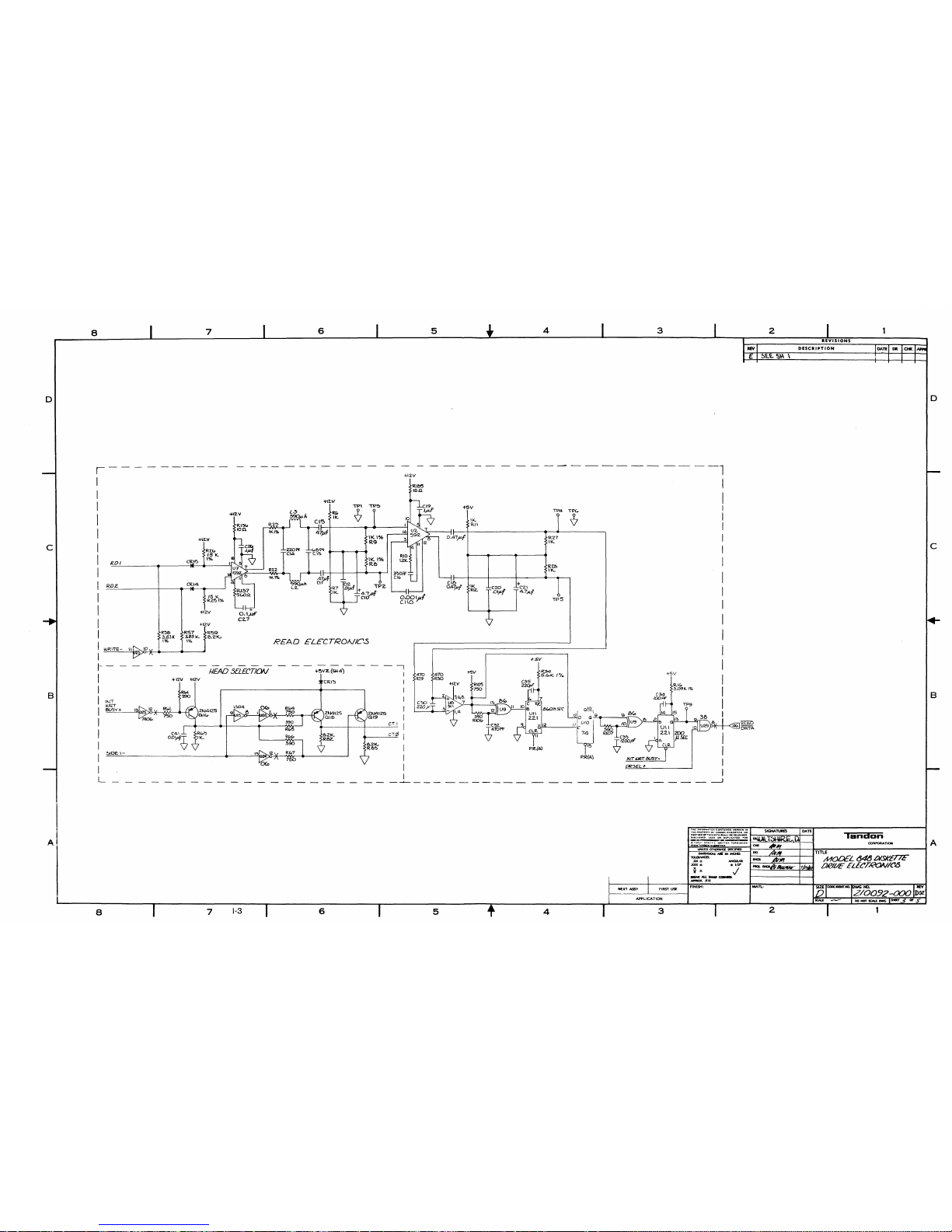
8
7
6
5
4
3
2
1
REVISIONS
ftS!i
DESCRIPTION
D D
,----------
4-12V
-----------------1
Rltf.5
loa
+\'Z.V
W4
TPc..
~
R27
IK-
e
RU>
IK...
+
C'2\
4.7ft.f
TP5
IK
RIZ,.
o.OOljtt
C.IIO
R7
C..o121
l'
TP2.
!).IT +
IK.
~i"J#f
READ
£LECTROA/IC..s
+IZ.V
TP\
T5V
~.A-LA
Rr..
~
IK..
CI5
II<-.
R2~
RII
11<.1%
47p.f
4-
0.1#
C2..7
R'l.lD
'5K..
1%
+l2.V
+\2.V
CRl4
CR.I':'>
-t12V
R57
R'59
3.53K.B.'2
K.J
1%
R~
3.831(
1%
RDZ
I?DI
e
B
RI<D
3.091(1%
(.34
trow
-+5V
o!Q.,
/2
0
G'~9
9
BCD
~
..:../.:../I
C
UIO
I
~
10
lJ'3
9
4 RIO?
C~~
T
'2OO
pf
l!l
\l
P.R(A)
tNT
UJRT
BUSY-
OR5EL+
RIO'5
7'30
t5V
+IZ.V
470
R~
CY)
220.JJ
470
R'29
-
--I
I
I
I
I
I
I
C.T
I I
CTa!
I
I
I
I
I
J./£IiD
SELECTION
WR\TE-
II
1-----
I
I
liNT
WR.T
I
13U5:..:.Y---'-+_-----'~.
I
I
I
I
~OEI-
I
L
8
APPLICATION
8
7
1-3
6
5
4
NEXT
ASSY
FIRST
USE
3
FINISH:
MATL:
SIGNATURES2DATE

8
7
6
5
4
3
2
D
8
c
I
--i
I
I
I
-~
2
+Z4V
MATL:
+24
V
C~9
CR7
CR~
-1
I
I
I
P4
14 /2
fD>..:------+--:--------...::4"77-:w'
STEPN1DTOR.
/5 I
~I
I
WIND/Ala
I
UUJ2.074B
~
(TYP4~f'N)4,5,12,1:!
&NO
I I ! I
M I I
c~c;,
I I I
1~400~(TYP4PL)
I I I
I 1
I I :
'I
I
I
DST£PMD~
r--""""'/
~
UJIA/DIAlCT
.2
L_J
R4/
~.31(,
~24V
+Z4V
'*
RESISTOR L(J{'ATEO
ltV
SANtE
RESISTOR
PA
C'K,
FINISH:
FIRST USE
NEXT
ASSY
APPLICATION
3
-H2V1{s1l~
R:?>7
4.71<.
5'TPEI'\1+
DRSEL
+-
P.R.(A)
P.
R.
(A)
4
~/2V
TPEl
POR.-
tSV
(8.9.
Z2,
23,
Zs.~3t
~
42,
4!J.44IO!},
GND
~
I
U9
}=2>~
+-=:.w
RZ
zzo
.!iw
WRITE-
5
LV
OIR+
Sl-(
1.
Die
POWERJ
CONNECTOR.
P7
r---'
r-'
I
[§>-+1--+1~»:>-.L:'5~--1
I
:
[D:
:
)31:
2
+~
Im~
I!)
I .
l!l
__
Z_PL
_
I I 4
CI
CC65,
7CD
_4.7$y
lO.lul
I I
'1+
50
Y
(TTP
ZPl.)
I 1
>>-~II:..-_-.
.:..:+Z;;...:.411
L-.J
L - _...J POIJJER.
REF.
~NECTlJI2-
ONLY)
PAD-S
~5)
_
poWER
TURN
oFF
,-----
J
I
6
----------------------1
r
+5
__
I
I
I
L
I
RP4
Z
4:TK.
+5V
+5V
5
RP4
4.71(.
"
RP:3
47DK.
I Z
1-4
TP7
7
221<.
RP2
VPD2 I
8
TR~CK¢
lOR\TE.
PROTEC,
VPD
5 " 5
CD
SE~OOR.
~~
1J,~K..
ELECTRON\C51
.L-
- _
I
I
I
I
P3
I
~
~4
~
+5V
WR\T£
_;
I I
150
PRO'TECT
/""
I I
I
L.E.D.
~
IlURI1E
"'F:t):'
~5V
I
PRDTECT
I I
SENSOR
>-'~1---"""'7
_.-
--!o!~f\:>.:T:1
L_
J
)Po
......
...----'
,-
- -
-;,-
- - -
r-,
Rt>4
ITR~CK.
EJ:I
~
+SV
I
(l)
/ I
I~
I
L.E.O
:
)>-r':
=--------,~
I I
I
n'AC~
~)>-7:=2_-----.+5V
(/J
r l I
I~£~SOR.
~~I~I
---..--+-----4
I I
RP5
'
I
L_.J
Z2K.
Z,
8
c
D
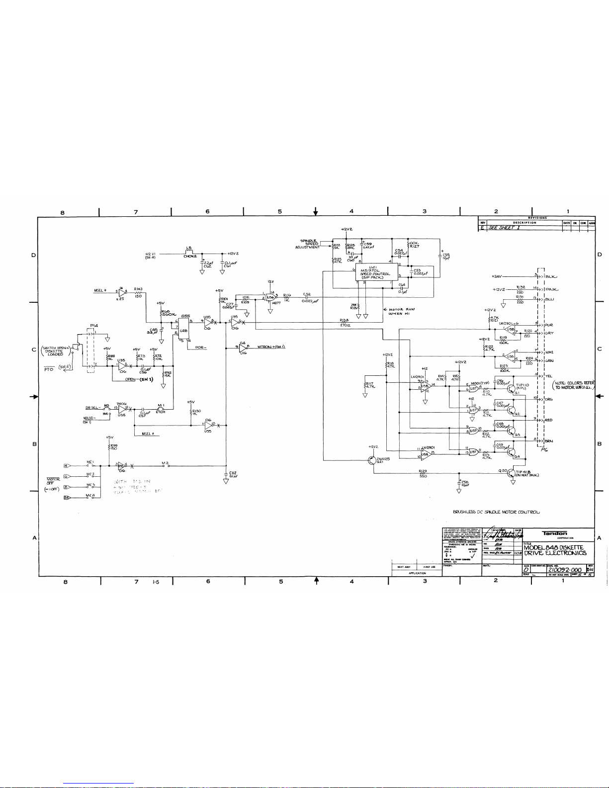
8
7
6
5
4
3
2
~12VZ.
REV
REVISIONS
DESCRIPTION
SE£SH££T
1
B
D
c
+\ZV2--~V'2.
14!»lpl~K....
220
I I
~
RI~I
I?J>BUJ
zzo
I
I I
i I
1 I
1-=-
__
--=::.5+-7
1
>:
PUR
I
I-=-_.,AN~~
>I
C:rRY
I
I
I
I
P----~>IWHI
I
~_-vvv--~
>I
uRN
I
I
.------
----..:.:.~>:
YEL
J
(~O\E~
COLORS
R£ftR
I10MCSfOR
WtR\N6.
I
.----
.......
--+---=-=-j-7>
:ORU
I
I
I
r-----.--I-----'-~>
I
RED
I
I
I
r----
.......
--+.,----=::...~>
IBR~
l_J
p~
Q2.0
r-'
+Z4v-------=-~HI»
I
BLK...>
l I
R\22
4.7K.
+12V2.
+12V2.
cst:>
~'Q.uF
4-12V2.
RIIS
4.7K:
+
C55
-10)4
K\l4
4:TK..
14
RIZ9
-C5?J
-O.022,IAf
+12
lOOK,
R.\2.7
C54
o.oZ:Z,lJ-f
4
+12V2.
21\\4\2.5
QZI
+IZV2.
5
UAI
M51970t..,
!:PEED COAJTROL
(SIP
PACK..)
7
R\~3
Rlztl
+C59
SK. ZOK.
O.41Pf
+
RIZ5
~
47K.
C 0
5P\~DLE.
SPH:O
AOJU5TMENT
R\\CD
IK.
12.V
MTROt-J
+
9-\
\\
CII2
7o.
,
.u.f
RIlE>
4:7K,
RI\7
4.7K..
f+
12VZ
TjO.\~'"
'\leCoI
+l~77~U~':
1
O.047#f~-
I
U~5
\1
~4--....---,5=-l
')(~(,,~_~
+
__
-:R~~a=--
--J
l.70Q
U~5
0(0
POR-
+5V
565
~
7
2,
U2fl
RCDe>
SCoOK"
"
+5V
MSEL+
+12 VI
(S\.I4)
+SV
+5V
R7Zo
10K.
',J
2~:··'~'~:
I.""r
0<0
u25
-':-
'.)"
~
~.I,
/"
L...-_=:OPE~N
-($'"
1)
1<:.99
150
+5V
+5V
MSEL+
06 (,
R/43
_-=--
__
-'5.,
~l--__.fVV
..........
150
-3
1\1\2-
b-
--+---=::.tJ!l5)ci~I?------_o
o--------------f
~
740CD
DR&.L-r:~
~
k-::.-/\
T
_Q.I"ar
fiJ..~O
OO~-~1U~
e~
~
(5"
\)
-------------
......
-----'-'1"
"')(':)'-0---4-_
..
Mel
~
,'-,
0
[§:>
MCZ
0
MOTOR
DrF
MC~
(-=Off)
~
0
1M>
MC4
0
B
c
(S't5\~~~::)I
\ LOADED
PTO
(SHb)
D
APPLICATION
3
A
CORPORATION
landan
2
MATL:
TITLE
1-1NQl-..D2C!.._~-t
MOOELM8
D\5KETTE.
~~~----+~
DR\V~
El.£CTROt\1\C&
DIMENSIONSININCHES
'IOIJIlANCIS:
.xx:t:
NGAM
JOO(:t:
:to
I~
~:t:
.;
_ALl_~
-'.10
"rMI:
'.I'O
......
T!O,.
(OlllfA''''I:D
MI:.I:O,.
l'
T",.
".O"IIRT't'OFT
_00"MA••
CTte.
"0
:~T..-::l[~T=:-:.._:'~~::::_~~
I---.if.-.;l,l~¥-,t~""""r--:""",
~:~~~'Jf"'tJr;.~
l-X~tlLlftA;lIliIililjli~~
...0...
1''''....
•
FINISH:
FIRST USENEXT ASSY
4
5
6
1-5
7
A
8


APPENDIX
II
RECOMMENDED
SPARE
PARTS
LIST

PARTS
AND
SUBASSEMBLIES
Part
Drive
Belt
Drive
Motor
Circuit
Board
Cone
Assembly
Diskette
Lever
Bridge
Assembly
Bezel
Activity
L.
E.
D.
(Front
Panel)
Load
Arm
Assembly
Track00Sensor
Assembly
Write
Protect
Sensor
Assembly
Door
Open
Switch
Assembly
Index
Sensor
Assembly
Diskette
Ejector
Assembly
Head
Carriage
Assembly:
Single-Sided
Recording
Double-Sided
Recording
Stepper
Motor
(Mounting)
Assembly
Stepper
Band
Load
(Power)
Resistors
Diskette
Lever
Lock
Ejector
Spring
Load
Arm
Spring
Note
All
components
are
standard
commercial
parts
purchasedtooriginal
equipment
manufacturer's
specifications.
Part
Number
210062-000
210061-000
210094-000
210085-000
210084-000
210086-000
210011-000
210081-000
210089-000
210080-000
210079-000
210083-000
210075-000
210124-000
210065-001
-
210065-002_
210090-000
210112-000
210076-000
210082-000
210036-000
210122-000
OEM
OPERATING
AND
SERVICE
MANUAL,
TM848-1
AND
TM848-2
THINLINE™DISK
DRIVES,
48
TPI,
TANDON
PIN
179031-001
ALIGNMENT
DISKETTE
Recommended:
Dysan
8006~0,
Model
Number
360/2A
"
-1

PIN
1.7~031-001
(1082)
 Loading...