

Page 1
n
n
n
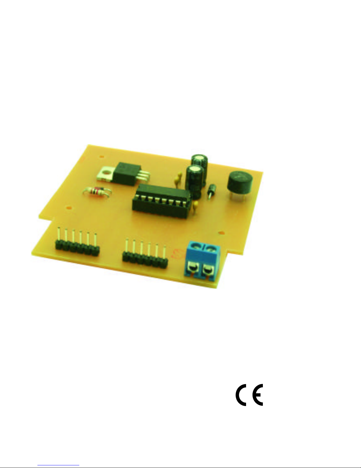
s88-Booster
n
S88-2
n
Anleitung
n Manual
n Mode d´emploi
n Handleiding
n
Art.-Nr. 21-01-078 / 22-01-078
n
n
Page 2

n
n
n Deutsch 3
n English 19
n Français 35
n Nederlands 51
n
n
n
n
n
n
n
n
n
© 09/2006 Tams Elektronik GmbH
Alle Rechte, insbesondere das Recht der
Vervielfältigung und Verbreitung sowie der
Übersetzung vorbehalten. Vervielfältigungen
und Reproduktionen in jeglicher Form
bedürfen der schriftlichen Genehmigung
durch die Tams Elektronik GmbH.
Technische Änderungen vorbehalten.
© 09/2006 Tams Elektronik GmbH
All rights reserved. No part of this
publication may be reproduced or
transmitted in any form or by any means,
electronic or mechanical, including
photocopying, without prior permission in
writing from Tams Elektronik GmbH.
Subject to technical modification.
© 09/2006 Tams Elektronik GmbH
Tout droits réservés, en particulier les droits
de reproduction et de diffusion ainsi que le
traduction. Toute duplication ou
reproduction sous quelque forme que ce soit
nécessite l´accord écrit de la societé Tams
Elektronik GmbH.
Sous réserve de modifications techniques.
© 09/2006 Tams Elektronik GmbH
Alle rechten voorbehouden. Niets uit deze
publicatie mag worden vermenigvuldigd
opgeslagen of openbaar gemaakt, zonder
voorafgaande schriftelijke toestemming van
Tams Elektronik GmbH.
Technische wijzigingen voorbehouden.
n
Page 3

S88-2 English
Page 19
Table of contents
How to use this manual 20
Intended use 20
Safety instructions 21
EMC declaration 23
Operation overview 23
Technical specifications 24
Checking the package contents 25
Required tools and consumables 25
Safe and correct soldering 25
Assembling the kit 27
Performing a visual check 30
Performing a functional test
and connecting the s88-Booster 31
FAQ 32
Manufacturer's note 33
Certification 33
Conditional warranty 33
Parts list I
Printed Circuit Board (PCB) layout (Fig. 1) II
Connections (Fig. 2) III
Circuit Diagram (Fig. 3) IV
(Pages I to IV in the centre of this handbook are removeable.)
Page 4

English S88-2
Page 20
!
How to use this manual
If you have no specialist technical training, this manual gives step-bystep instructions for safe and correct assembly of the kit and fitting of
the ready-built module, and operation. Before you start, we advise you
to read the whole manual, particularly the chapter on safety
instructions and the FAQ chapter. You will then know where to take
care and how to prevent mistakes which take a lot of effort to correct.
Keep this manual safely so that you can solve problems in the future. If
you pass the kit or the ready-built module on to another person, please
pass on the manual with it.
Intended use
The kit or the ready-built module can be assembled and operated with
a digital model railway using this manual. It reduces the interference
occuring in s88-bus lines during data transmission.
The kit and the ready-built module should not be assembled or fitted by
children under the age of 14.
Reading, understanding and following the instructions in this manual
are mandatory for the user.
Any other use is inappropriate and invalidates any guarantees.
Caution:
The circuit contains integrated circuits. These are very sensitive to static
electricity. Do not touch components without first discharging yourself.
Touching a radiator or other grounded metal part will discharge you.
Page 5

S88-2 English
Page 21
Safety instructions
Mechanical hazards
Cut wires can have sharp ends and can cause serious injuries. Watch
out for sharp edges when you pick up the PCB.
Visibly damaged parts can cause unpredictable danger. Do not use
damaged parts: recycle and replace them with new ones.
Electrical hazards
§ Touching powered, live components,
§ touching conducting components which are live due to malfunction,
§ short circuits,
§ connecting the circuit to another voltage than specified,
§ impermissibly high humidity,
§ condensation build up
can cause serious injury due to electrical shock. Take the following
precautions to prevent this danger:
§ Never perform wiring on a powered module.
§ Assembling and mounting the kit should only be done in closed,
clean, dry rooms. Beware of humidity.
§ Only use low power for this module as described in this manual and
only use certified transformers.
§ Connect transformers and soldering irons only in approved mains
sockets installed by an authorised electrician.
§ Observe cable diameter requirements.
§ After condensation build up, allow a minimum of 2 hours for
dispersion.
§ Use only original spare parts if you have to repair the kit or the
ready-built module.
Page 6

English S88-2
Page 22
Fire risk
Touching flammable material with a hot soldering iron can cause fire,
which can result in injury or death through burns or suffocation.
Connect your soldering iron or soldering station only when actually
needed. Always keep the soldering iron away from inflammable
materials. Use a suitable soldering iron stand. Never leave a hot
soldering iron or station unattended.
Thermal danger
A hot soldering iron or liquid solder accidentally touching your skin can
cause skin burns. As a precaution:
§ use a heat-resistant mat during soldering,
§ always put the hot soldering iron in the soldering iron stand,
§ point the soldering iron tip carefully when soldering, and
§ remove liquid solder with a thick wet rag or wet sponge from the
soldering tip.
Dangerous environments
A working area that is too small or cramped is unsuitable and can cause
accidents, fires and injury. Prevent this by working in a clean, dry room
with enough freedom of movement.
Other dangers
Children can cause any of the accidents mentioned above because they
are inattentive and not responsible enough. Children under the age of 14
should not be allowed to work with this kit or the ready-built module.
Little children can swallow small components with sharp edges, with
fatal results! Do not allow components to reach small children.
In schools, training centres, clubs and workshops, assembly must be
supervised by qualified personnel.
In industrial institutions, health and safety regulations applying to
electronic work must be adhered to.
Page 7

S88-2 English
Page 23
EMC declaration
This product is developed in accordance with the European standards
EN 55014 and EN 50082-1, tested corresponding to the EC - directive
89/336/EWG (EMVG of 09/11/1992, electromagnetic tolerance) and
meets legal requirements.
To guarantee the electromagnetic tolerance you must take the
following precautions:
§ Connect the transformer only to an approved mains socket installed
by an authorised electrician.
§ Make no changes to the original parts and accurately follow the
instructions, circuit diagram and PCB layut included with this manual.
§ Use only original spare parts if you have to repair the kit or the
ready-built module.
Operation overview
The s88-Booster reduces the interferences occuring during data transfer
from the s88-feedback modules to the receiver (central unit, PC via
interface or memory). Interference is caused by external electrical
signals such as:
§ switching impulses for points or
§ digital signals in data lines running in parallel to the bus lines.
This interference affects the data transfer and causes faulty input to the
receiver.
Because it is standard to operate the s88-bus with a voltage of 5 V
interference voltages of 2,5 V can cause interference in data transfer.
The longer the s88-data lines are, the higher is the risk of interference.
The s88-booster is connected between receiver and s88-module(s) and
heightens the s88-bus´s supply voltage to 12 V. In consequence
interference voltages of less than 6 V have non influence on the data
transfer in the s88-bus.
Page 8

English S88-2
Page 24
!
Most commercial s88-feedback modules (e.g. from Littfinsky, Märklin,
Viessmann, Tams) operate with this higher supply voltage.
Caution:
Before installing the s88-booster you must check if the s88-feedback
modules used in your model railroad layout can operate with a supply
voltage of 12 V. You can determine this by checking the IC-types used
on the feedback modules.
Modules with ICs with a type designation starting with number „74“:
These modules are not suitable to use with the s88-booster.
Highering the supply voltage to 12 V on the s88-booster would damage
these modules.
Modules with ICs with a type designation containing the numbers
„4014“ and „4044“: These modules are OK to use with the s88-booster.
Technical specifications
Supply voltage 12-18 Volt a.c. voltage
Supply voltage of the
connected s88-feedback modules 12 Volt d.c. voltage
Please note the info in the
section „Operation overview“!
Current consumption max. 500 mA
(depending on the number of
connected s88-feedback modules)
Protected to IP 00
Ambient temperature in use 0 - + 60 °C
Ambient temperature in storage -10 - + 80 °C
Comparative humidity allowed max. 85 %
Dimensions approx. 73 x 80 mm
Weight approx. 26 g
Page 9

S88-2 English
Page 25
!
Checking the package contents
Check the contents of the package for completeness immediately after
unpacking:
§ one kit, containing the components listed in the parts list (see page
I) and one PCB or
§ one ready-built module,
§ one 6-core ribbon cable with plugs,
§ one manual.
Required tools and consumables
Make sure you have the following tools, equipment and materials ready
for use:
§ an electronic soldering iron (max. 30 Watt) with a fine tip,
§ a soldering iron stand,
§ a tip-cleaning sponge,
§ a heat-resistant mat,
§ a small side cutter and wire stripper,
§ a pair of tweezers and long nose pliers (not necessary for the
ready-built module),
§ tin solder (0,5 mm. diameter),
§ wire (diameter: > 0,25 mm² for all connections).
Safe and correct soldering
Caution:
Incorrect soldering can cause dangers through fires and heat. Avoid
these dangers by reading and following the directions given in the
chapter Safety instructions. If you have had training in soldering you
can skip this chapter.
Page 10

English S88-2
Page 26
§ Use a small soldering iron with max. 30 Watt. Keep the soldering tip
clean so the heat of the soldering iron is applied to the solder point
effectively.
§ Only use electronic tin solder with a flux.
§ When soldering electronic circuits never use soldering-water or
soldering grease. They contain acids that can corrode components
and copper tracks.
§ Solder quickly: holding the iron on the joints longer than necessary
can destroy components and can damage copper tracks or
soldering eyes.
§ Observe correct polarity orientation of semi-conductors, LEDs
electrolytic capacitors and integrated circuits before soldering and
ensure that the solder time does not exceed 5 seconds, otherwise
components can be damaged.
§ Apply the soldering tip to the soldering spot in such a way that the part
and the soldering eye are heated at the same time. Simultaneously add
solder (not too much). As soon as the solder becomes liquid take it
away. Hold the soldering tip at the spot for a few seconds so that the
solder flows into the joint, then remove the soldering iron.
§ Do not move the component for about 5 seconds after soldering.
§ To make a good soldering joint you must use a clean and
unoxidised soldering tip. Clean the soldering tip with a damp piece
of cloth, a damp sponge or a piece of silicon cloth.
§ Cut the wires after soldering directly above the PCB solder side with
a side cutter.
§ After placing the parts, please double check for correct polarity.
Check the PCB tracks for solder bridges and short circuits created
by accident. This would cause faulty operation or, in the worst
case, damage. You can remove excess solder by putting a clean
soldering tip on the spot. The solder will become liquid again and
flow from the soldering spot to the soldering tip.
Page 11
S88-2 English
Page 27
Assembling the kit
You can skip this part if you have purchased a ready-built module.
Preparation
Put the sorted components in front of you on your workbench. The
separate electronic components have the following special features you
should take into account to prevent mistakes in assembling:
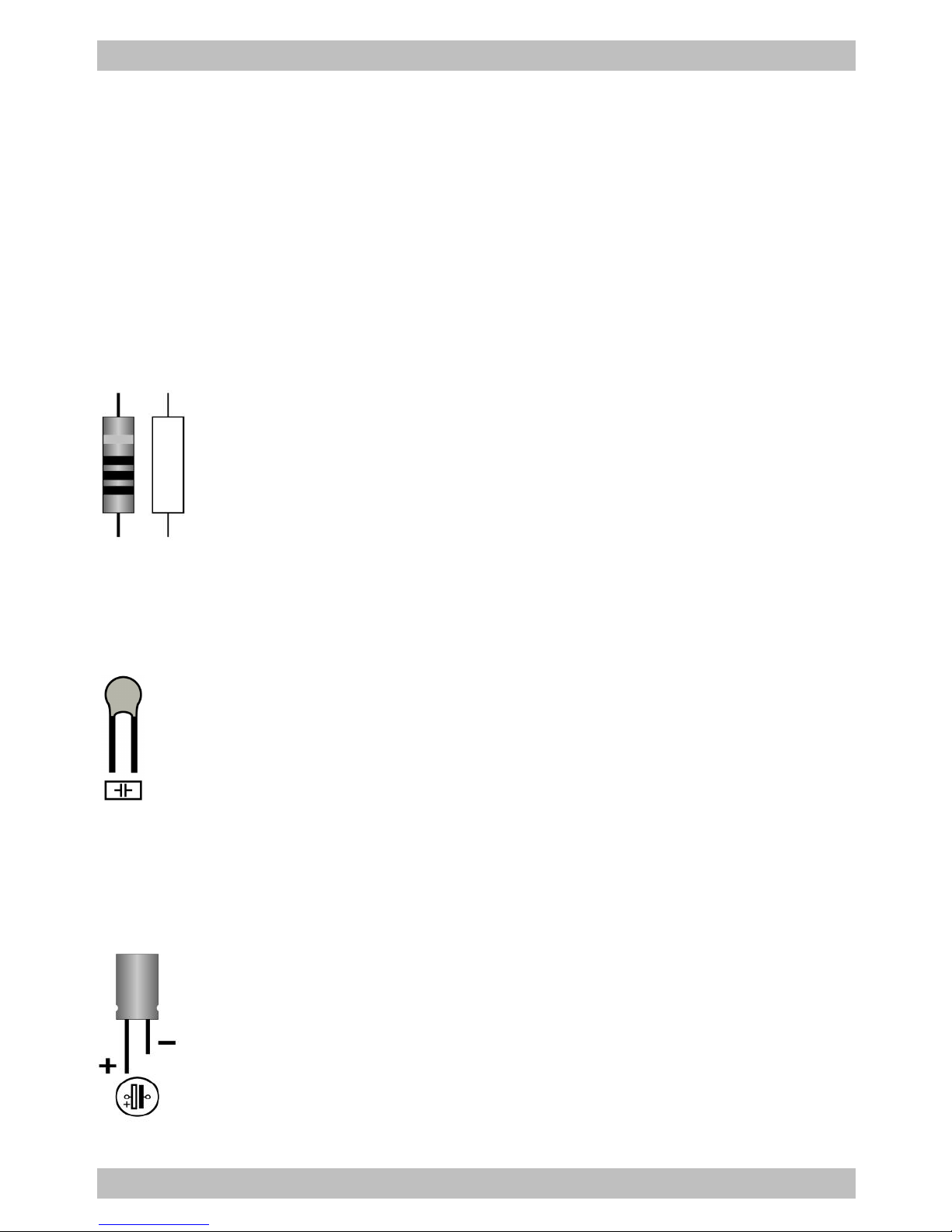
Resistors
Resistors reduce current. Their mounting orientation is of no
importance. The value of resistors for smaller power ratings
(under 5 W) is indicated through colour rings. Every colour
stands for another figure. The colour ring in brackets indicates
the tolerance of the resistor which here is of no importance.
Value Colour rings
1 kΩ brown - black - red (gold)
Capacitors
Among other things capacitors are used for filtering interference
voltages or as frequency determining parts. Ceramic capacitors
are not polarized, for that reason their mounting orientation is
of no importance. Normally they are marked with a three-digit
number which indicates the value coded.
Value Number
100 nF 104
Electrolytic capacitors
Electrolytic capacitors are often used to store energy. In
contrast to ceramic capacitors they are polarized. One of the
two leads is marked with a minus sign which indicates the
mounting orientation. The value is given on the casing.
Electrolytic capacitors are available with different voltage
sustaining capabilities. Using an electrolytic capacitor with a
Page 12
English S88-2
Page 28
voltage sustaining capability higher than required is always
possible.
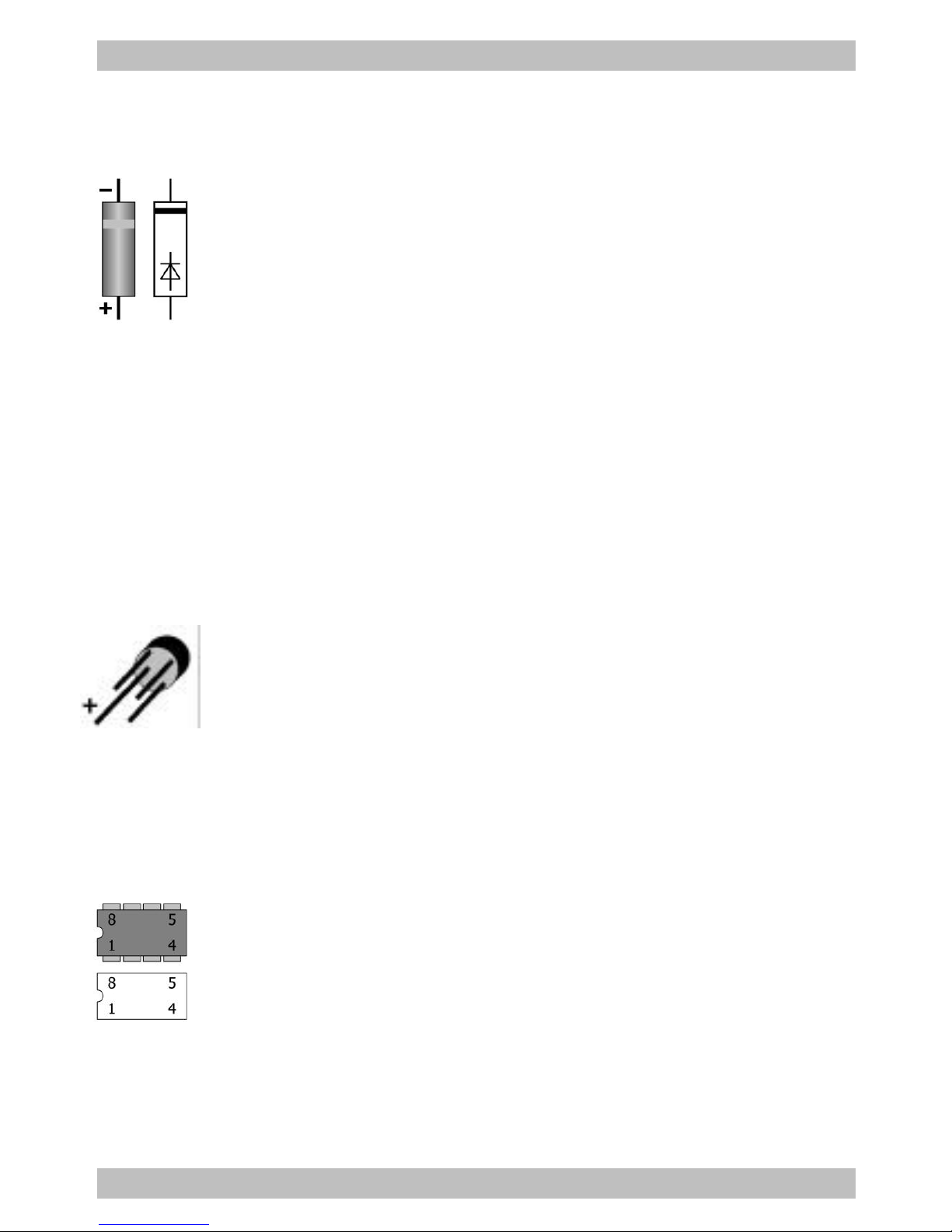
Diodes
Diodes allow the current to pass through in one direction only
(forward direction), simultaneously the voltage is reduced by
0,3 to 0,8 V. Exceeding of the limit voltage always will destroy
the diode, and allow current to flow in the reverse direction.
The diode type is printed on the body.
Diodes must be mounted in a given direction. The negative
end is marked with a ring. This is shown in the PCB layout.
Zener diodes
Zener diodes are used for limiting voltages. In contrast to
„normal“ diodes they are not destroyed when the limit voltage
is exceeded.
Rectifiers
Rectifiers convert alternating into direct voltage, they have
hardly no influence on the level of the voltage. They have four
pins: two for the input voltage (a.c. voltage) and two for the
output voltage (d.c. voltage). The pins for the output voltage
are polarized. The pin connections are printed on the housing.
As usual with wired components the longer connecting pin is
the positive pole.
Integrated circuits (ICs)
Depending on the type, ICs fulfil various tasks. They are
polarized and therefore have to be mounted in a certain
direction. The most common housing form is the so-called
"DIL"-housing, from which 4, 6, 8, 14, 16, 18 or more "legs"
(pins) are arranged along the long sides. The mounting
orientation is shown by a semicircular or circular marking at
the end of the housing, which is also shown on the PCB
layout.
Page 13
S88-2 English
Page 29
!
ICs are sensitive to damage during soldering (heat,
electrostatic charging). For that reason in the place of the ICs
IC sockets are soldered in, in which the ICs are inserted later.
The mounting orientation of the sockets is preset as well. The
markings on the PCB, the socket and the IC must lie on top of
each other after mounting.
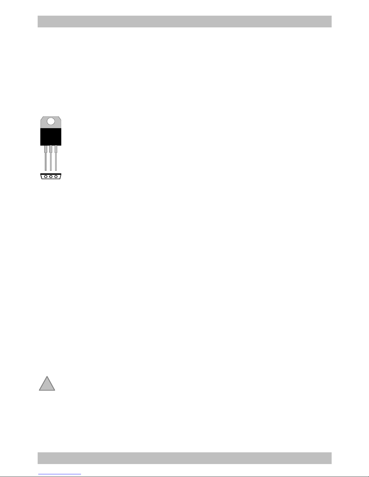
Voltage regulators
Voltage regulators are ICs, which convert a variable, non
regulated input voltage in a constant output voltage. They are
produced in transistor housings with three connecting pins for
input, output and earth.
With voltage reuglators in a flat TO-housing the unlabelled
metallic rear is marked by a thick line on the PCB layout.
Terminal strips
Terminal strips are solder-in screw-type terminals. They provide a
solder-free and safe connection of the cables to the circuit, which can
still be seperated any time. When several terminal strips have to be
mounted side by side, they have to be put together before mounting.
Assembling the kit
Start the assembly with the resistor and the diodes. First solder the
components on the solder side of the PCB and then cut the excess
wires with side cutters, as short as possible.
Then insert and solder in the IC-sockets The socket must be mounted
according to the marking on the PCB. Continue the assembly with the
rectifier, the capacitors, the voltage regulator and the electrolytic
capacitors.
Caution:
Diodes, ICs, rectifiers, voltage regulators and electrolytic capacitors
must be mounted in the right direction! If you solder them the wrong
way around the affected parts can be damaged when you connect the
Page 14

English S88-2
Page 30
!
!
power. In the worst case the whole circuit can be damaged, and at the
best, a wrongly connected part will not function.
Next solder the terminal strips and the solder pins. Join the terminal
strips together before soldering.
Finally, insert the ICs into the soldered IC-sockets.
Caution:
Do not touch the ICs without first discharging yourself by touching a
radiator or other grounded metal parts. Do not bend the "legs" of the
ICs when inserting them into the sockets. Check that the markings on
the PCB, the socket and the IC are in the same direction.
Performing a visual check
Due to material defects and / or improper assembly there may be risks
of injury. Transport damage to ready-built modules is also possible. So
you must perform a visual check after the assembly or after unpacking
the module.
Caution:
Do not power up the module yet.
The following points are inapplicable if you have purchased a ready-
built module.
§ Remove all loose parts, wire ends or drops of solder from the PCB.
Remove all sharp wire ends.
§ Check that solder contacts which are close to each other are not
unintentionally connected to each other. Risk of short circuit!
§ Check that all components are polarised correctly.
When you have remedied all faults, go on to the next part.
Page 15

S88-2 English
Page 31
!
!
Performing a functional test and
connecting the s88-booster
Please note:
Before installing the s88-booster you should check if the s88-feedback
modules used in your model railroad layout are compatible with a
voltage supply of 12 V and so with the s88-booster. Please note the
section „Operation overview“!
Checking the s88-feedback modules
You should check if the s88-feedback modules are working properly
before connecting them to s88-booster. See the manual for the s88feedback modules. That way you can prevent faults occuring after
installing the s88-booster due to the s88-feedback modules. Avoid
interference caused by external electrical signals during the funtionl
test.
Connecting the s88-booster
Disconnect the first s88-feedback module from the receiver (central
unit, interface, memory). Next connect the s88-booster to the receiver
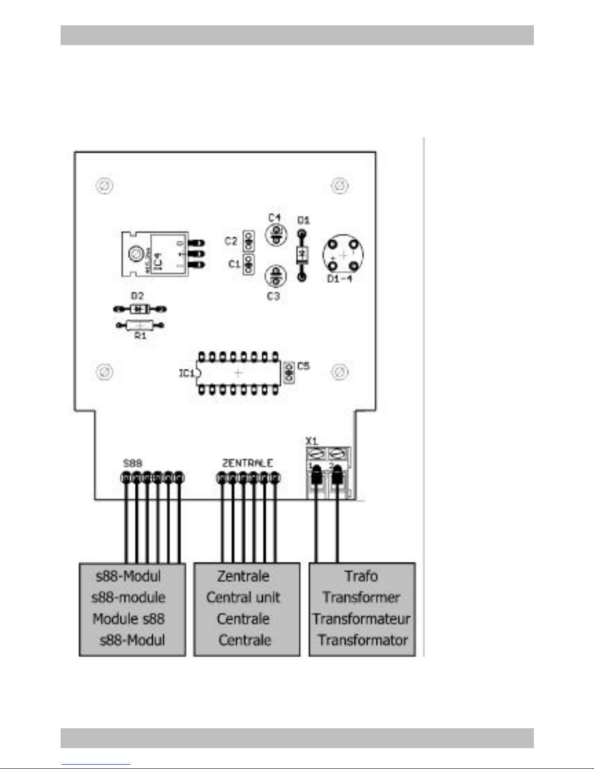
and the first s88-feedback module. Follow the connections diagram
fig. 2.
Caution:
The connections for the receiver and the s88-feedback module must
not be mixed up! If you connect the receiver to the terminal for the
s88-feedback module and the s88-feedback module to the terminal for
the receiver, damage to the connected devices may occur when starting
up!
Finally connect the s88-booster to it´s power supply.
Page 16

English S88-2
Page 32
!
!
Caution:
The s88-booster must be supplied by a transformer of it´s own. In case
the s88-booster is connected to a transformer that also supplies other
parts of the layout, short-circuits and damages at the s88-booster
cannot be excluded.
At last perform a function test on the connected s88-feedback modules.
FAQ
§ Parts are getting too hot and/or start to smoke.
Disconnect the system from the mains immediately!
Possible cause: one or more components are soldered incorrectly.
à Perform a visual check.
§ The receiver (central unit, interface, memory) does not recieve data
from the s88-feedback module.
Possible cause: The power supply of the s88-booster has been
interrupted. à Check the connection.
Possible cause: The IC on the s88-booster´s PCB has been
mounted the wrong way about. à Check the polarity.
Possible cause: The connections of the receiver and the s88-feedback
modules have been mixed up. à Check the connections. In this case it
is possible the connected devices having been damaged. Check these
without connecting them to the s88-booster.
If you cannot find the problem, please return the module for repair
(address on the cover page).
Page 17

S88-2 English
Page 33
Manufacturer's note
According to DIN VDE 0869, the person who builds this kit or brings the
circuit into operation is the manufacturer of the product. If he sells the
product to another person he is responsible for passing on all the
relevant papers. Domestic appliances assembled from a kit are deemed
industrial products and must comply with health and safety regulations.
Certification
This product conforms with the EC- directive 89/336/EWG on
electromagnetic radiation and is therefore CE certified.
Conditions of warranty
This product is guaranteed for two years. The warranty includes the
correction of faults which can be proved to be due to material failure or
factory flaw. As we have no control over the correct and proper
assembly and mounting we can only guarantee the quality of the
components and the completeness of kits. We guarantee the function
of the parts according to the parameters in not mounted state as well
as the adherence to the technical specifications of the circuit when
assembled and connected according to the manual.
Other claims are excluded. By law, we are not responsible for damages
or secondary damages in connection with this product. We retain the
right to repair, make improvements, supply spare parts or return the
purchase price.
The following invalidate the warranty:
§ using an unsuitable soldering iron, solder containing liquid acids or
similar,
§ if the kit is assembled and soldered poorly, or if damage is caused
by not following the instructions in this manual,
§ if the ready-built module has been altered and repair attempts have
failed,
Page 18

English S88-2
Page 34
§ if arbitrary changes in the circuit are made,
§ if the circuitry is changed in any way, through adding or omitting
wiring or components, or through modifying the circuit board,
§ if parts other then the original ones delivered with this kit are used,
§ if the copper tracks or soldering eyes are damaged,
§ when components are mounted incorrectly, or if the components or
the circuit are poled incorrectly, also subsequent damage resulting
from these faults,
§ if damage occurs due to an overload of the module,
§ if connected to a incorrect voltage or current,
§ if damaged by other persons,
§ if damaged by faulty operation or if damaged by careless use or
abuse,
§ if damaged by touching components before electrostatic
discharging of the hands.
Page 19
S88-2
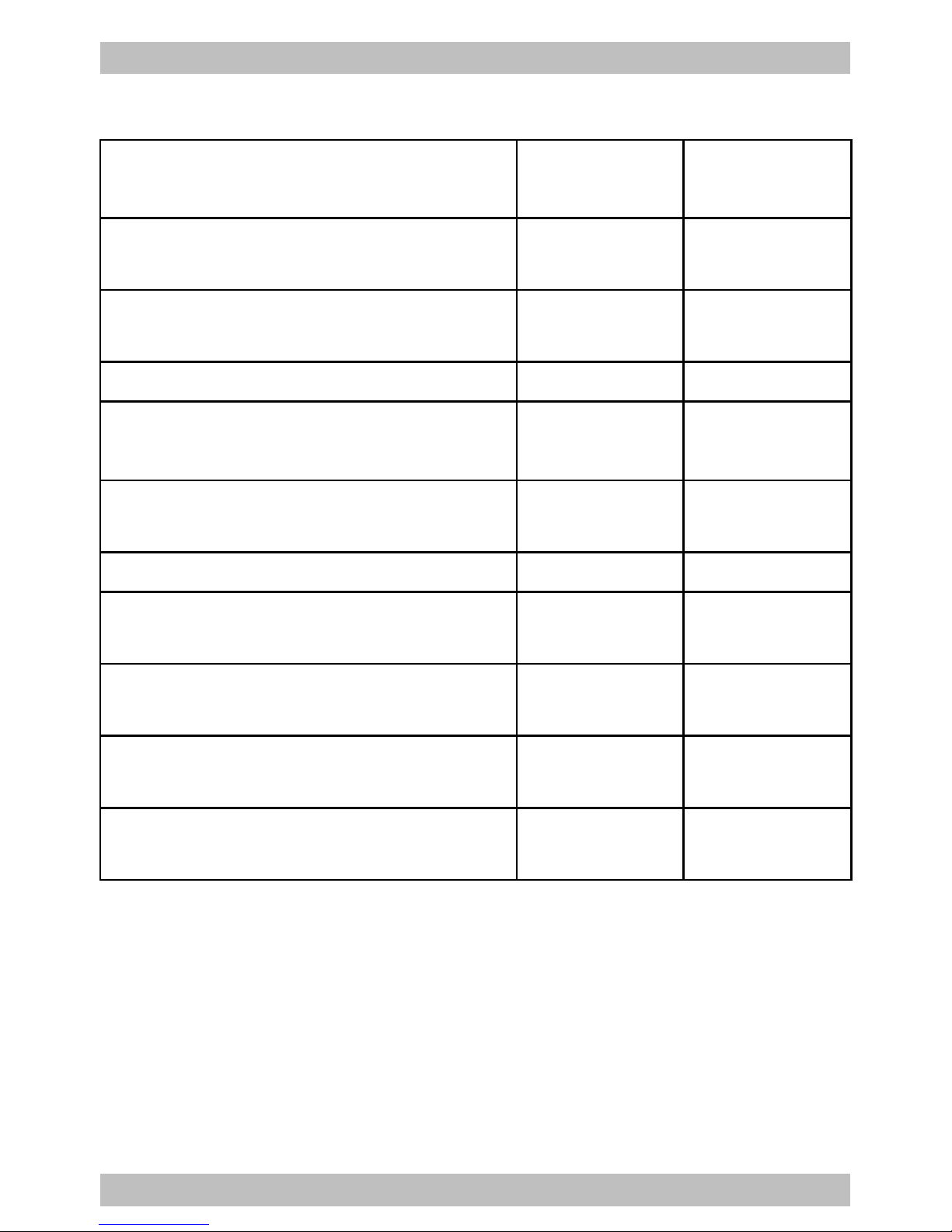
Stückliste - Parts list - Nomenclature – Stuklijst
Widerstände - Resistors
Résistances - Weerstanden
R1 1 k
Kondensatoren – Condensers
Condensateurs - Condensatoren
C1, C2, C5 100 nF
Elkos - Electrolytic capacitors
Condensateurs électrolytiques - Elco’s
C3, C4 100 µF/25 V
Dioden - Diodes D1 1N4004*
Zener-Dioden - Zener diodes
Diodes Zener -Zenerdiodes
D2 5V1
Gleichrichter – Rectifiers Redresseurs
- Gelijkrichters
D1-4 B80C800*
ICs – IC – CI– IC´s IC1 4104
IC-Sockel – IC-socket
Soquet IC – IC-voetje
IC1 16-pol.
Spannungsregler - Voltage regulators
Régulat. de tension - Spanningsregelaars
IC2 7812
Anreihklemmen - Terminal strips
Borniers - Printkroonstenen
X1 2-pol.
Stiftleisten - Solder pins
Barettes – Pinstrips
S88, ZEN 6-pol.
* oder ähnlich - or similar - ou équivalent - of gelijkwaardig
Seite - Page - Page - Pagina I
Page 20
S88-2
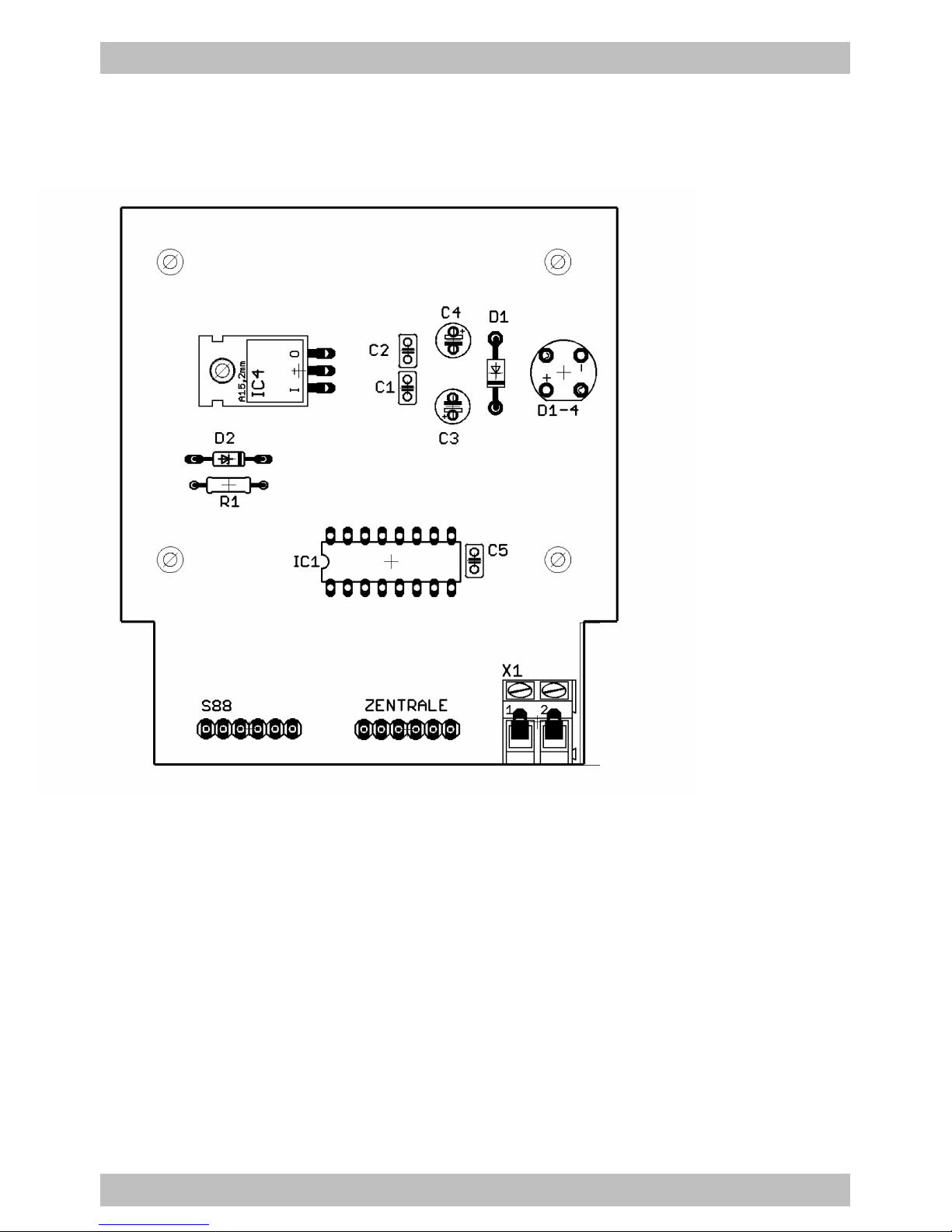
Fig. 1:
Bestückungsplan - PCB layout - Plan d´implantation - Printplan
Seite - Page - Page - Pagina II
Page 21
S88-2
Seite - Page - Page - Pagina III
Fig. 2:
Anschlußplan – Connections
Plan de raccordement – Aansluit plan
Page 22
S88-2
Seite - Page - Page - Pagina IV
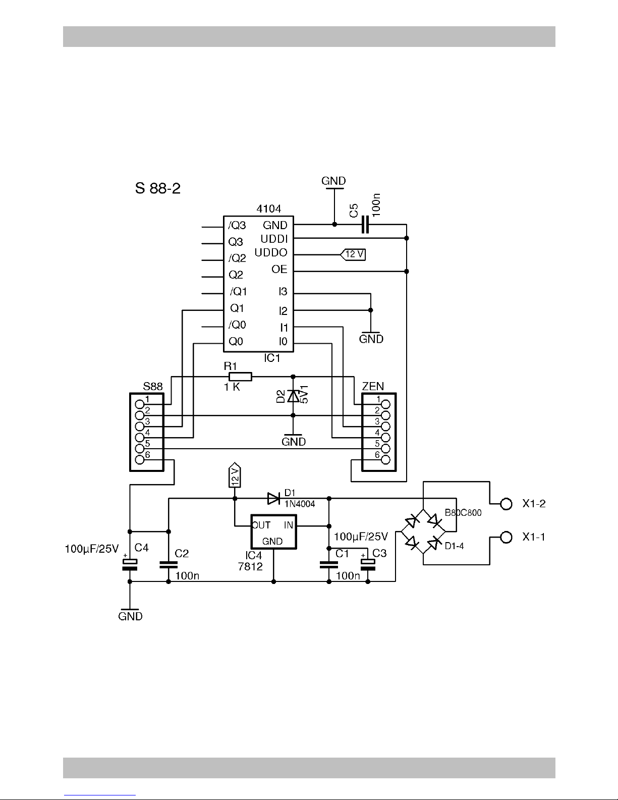
Fig. 3:
Schaltplan - Circuit diagram
Schéma de principe - Schakelschema
Page 23

n
n
n
Aktuelle Informationen und Tipps:
Information and tips:
n
Informations et conseils:
Actuele informatie en tips:
n
http://www.tams-online.de n
n
n
n
Garantie und Service:
Warranty and service:
n
Garantie et service:
Garantie en service:
n
n
Tams Elektronik GmbH
n
Rupsteinstraße 10
D-30625 Hannover
n
fon: +49 (0)511 / 55 60 60
fax: +49 (0)511 / 55 61 61
n
e-mail: [email protected]
n
 Loading...