TALER ADC100M, ADC100CA, ADC100C Datasheet

ADC100
Precision 22 Bit
Integrating A/D Converter
THALER CORPORATION • 2015 N. FORBES BOULEVARD • TUCSON, AZ. 85745 • (520) 882-4000
FEATURES
· 22-BIT RESOLUTION
· ±10.48 INPUT RANGE
· 1ppm/°C MAX. SCALE FACTOR ERROR
· 2 ppm MAX. LINEARITY ERROR
· AUTO ZERO
· BUS COMPATIBLE
· INTERNAL CLOCK and REFERENCE
· LOW POWER CONSUMPTION (0.4 WATTS)
DESCRIPTION
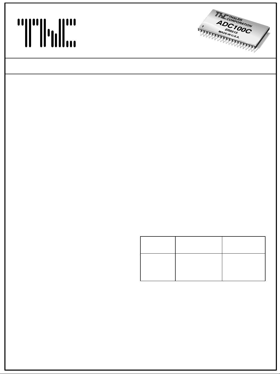
ADC100 is a high performance 22-bit A/D
converter based on a patented architecture
which provides outstanding performance
(accuracy) comparable to the best digital meters.
The ADC100 is available in two operating
temperature ranges, -25°C to +85°C and -55°C
to +125°C. "M" versions are screened for high
reliability and quality.
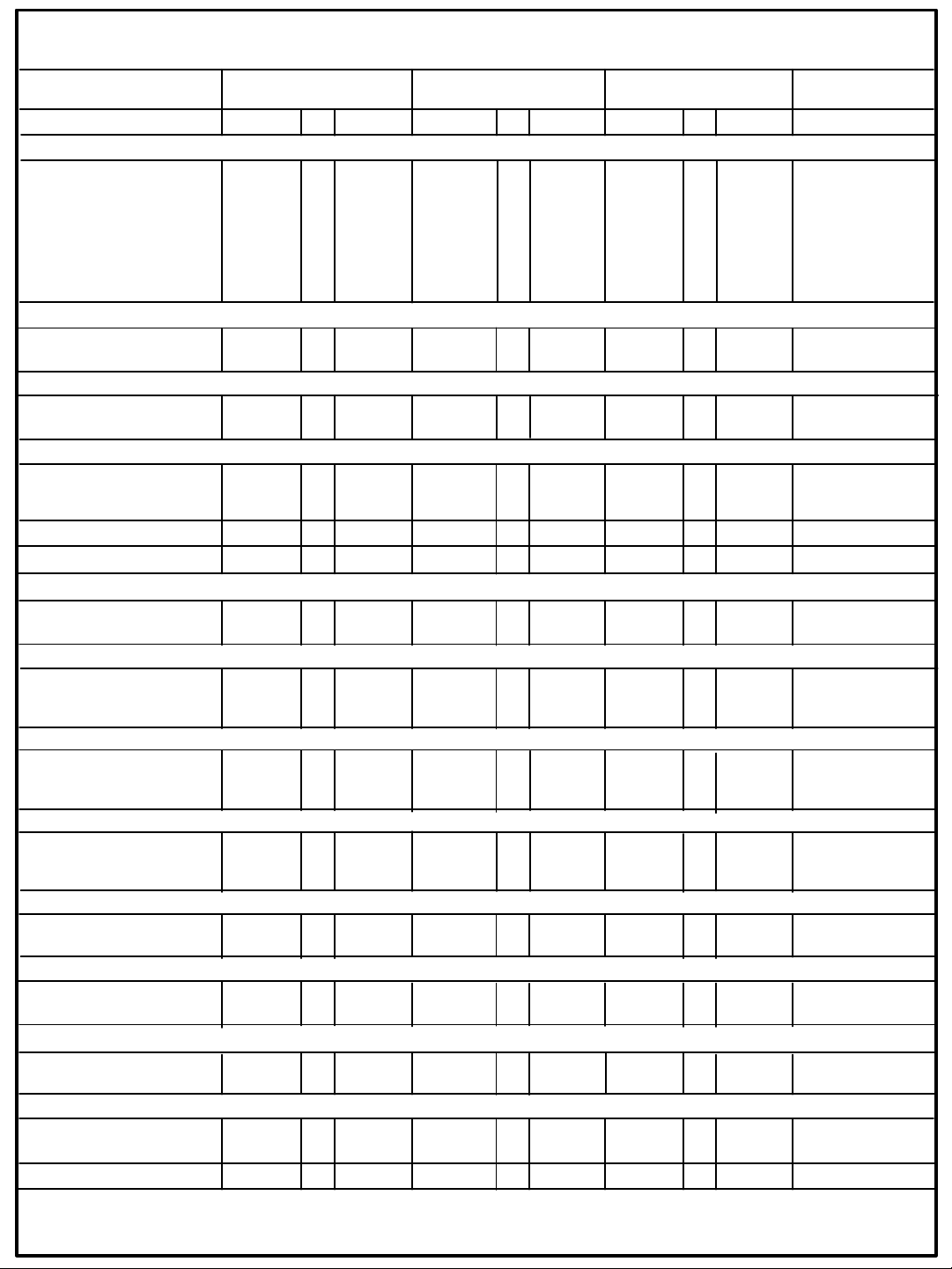
ADC100 offers 3 ppm max. linearity error and
1ppm/°C max. scale factor error over the military
temperature range. It also has excellent offset
stability at 2 ppm max. which the user can auto
zero if desired.
APPLICATIONS
· TEST EQUIPMENT
· DATA ACQUISITION
· SCIENTIFIC INSTRUMENTS
· MEDICAL INSTRUMENTS
· SEISMOLOGICAL EQUIPMENT
· ROBOTIC SYSTEMS
· WEIGHING SYSTEMS
Temperature Max. Scale
Type Operating Range Factor Deviation
ADC100C -25°C to +85°C 60ppm
ADC100CA -25°C to +85°C 30ppm
ADC100M -55°C to +125°C 100ppm
ADC100's compatibility with popular microcomputer buses increases its ease of application in smart
systems. An on-board microprocessor controls all internal functions of the ADC100. Thaler designers
have minimized external connections to greatly reduce the problem often encountered when applying
ADC's.
Operating from ±15VDC and a +5VDC power supply, ADC100 is packaged in a hermetically sealed 40pin ceramic DIP package. Precision test equipment, scientific and medical instruments, and data
acquisition systems are primary application areas for the unusually high resolution and accuracy of this
ADC.
ADC100DS REV. E MAR 00

MAXIMUM RATING SPECIFICATIONS ADC100
MODEL
PARAMETER
TEMPERATURE
Operating
Storage
POWER SUPPLY
V
CC
V
EE
V
DD
INPUTS
Analog Inputs
Digital Inputs
EXTERNAL CONNECTIONS
N.C.
N.C.
N.C.
Vee (-15V)
Vee (+15V)
Vdd (+5V)
GND
N.C.
N.C.
N.C.
1
2
3
4
5
6
7
8
9
10
(TOP VIEW)
ADC100
40
ANALOG LOW
39
ANALOG HIGH
38
N.C.
37
N.C.
36
N.C.
35
34
33
N.C.
N.C.
32
31
N.C.
MIN
-55
0
+14
-14
+4
V
EE
0
INTEGRATION
CAPACITOR
ADC100
MAX
125
160
+16
-16
+6
V
CC
V
DD
NOTES:
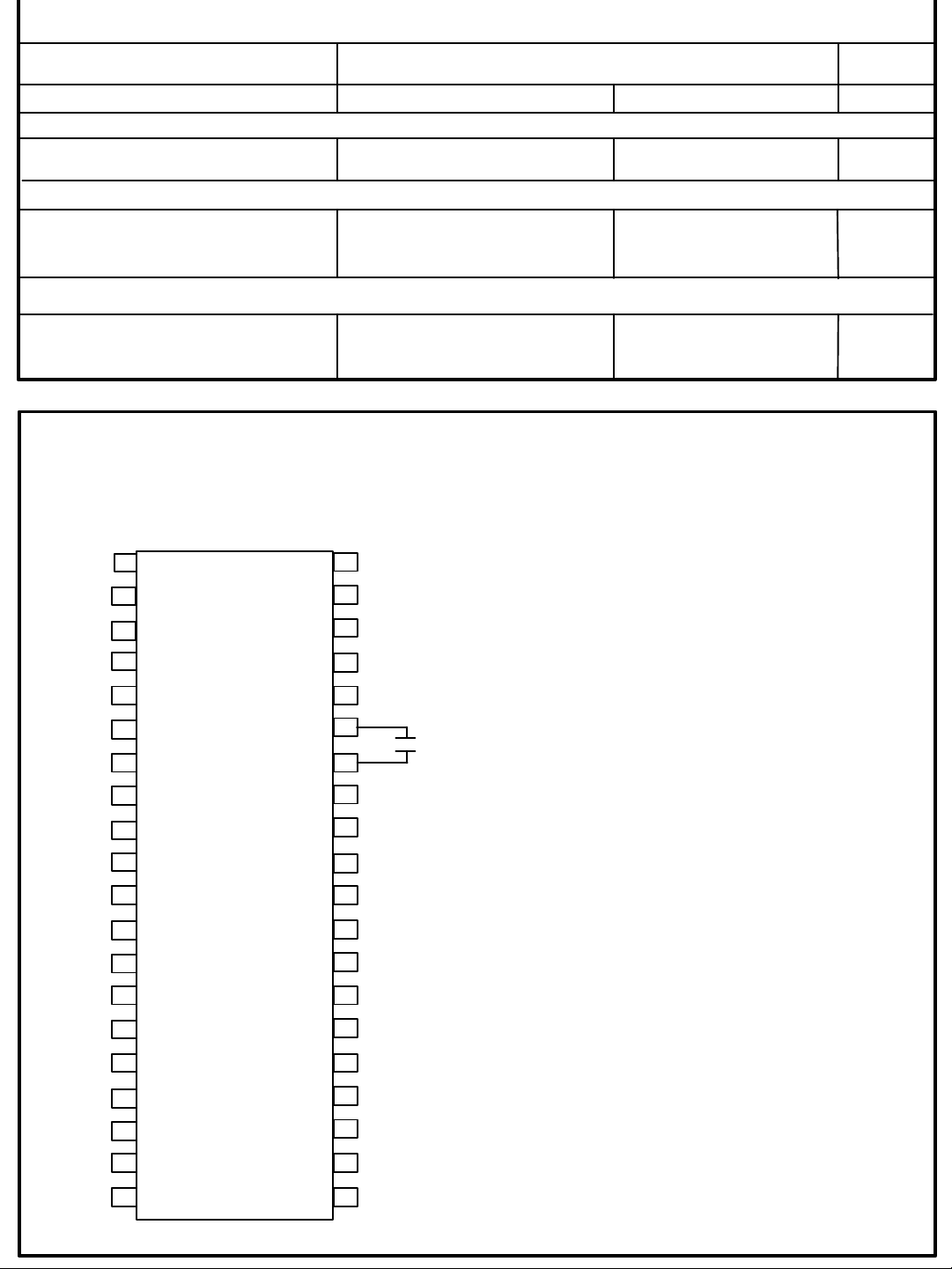
1. Power Supply Decoupling
The ADC100 has internal 0.1µF decoupling
capacitors for all power supply inputs. The
internal decoupling capacitors are adequate
for applications with relatively short power
supply leads (approx. 5") or if additional
capacitors are located on a circuit board.
For applications with long power supply
leads an external capacitor of 10 mF on the
+/- 15V inputs and 33 mF on the +5V input is
recommended.
2. Ground
The ground connection (pin 7) should be
made as solid as possible since ground
noise can result in a loss of accuracy. Use
of a ground plane is a good approach to
maintain the full accuracy of the ADC100.
UNITS
°C
°C
VDC
VDC
VDC
N.C.
N.C.
D0
D1
D2
D3
D4
D5
D6
D7
11
12
13
14
15
16
17
18
19
20
30
N.C.
AUTO ZERO
29
RESET
N.C.
28
N.C.
27
N.C.
26
25
N.C.
24
STATUS 1
23
STATUS 0
CONVERT
22
21
OUTPUT ENABLE
3. External Components
A 0.68 µF polystyrene integration capacitor
must be connected to pins 34 and 35 with a
lead length not exceeding 2".
4. Analog Inputs
In order to avoid differential noise pickup it is
recommended to use parallel adjacent lines
for the analog inputs (pins 39, 40) on PC
boards and shielded lines outside of the PC
connections.
ADC100DS REV. E MAR 00

ELECTRICAL SPECIFICATIONS
(Vps = +/- 15V, + 5V, T = 25 Deg. C.)
ADC100
MODEL
PARAMETER
ACCURACY
Resolution
Input Equivalent Noise
Offset without Auto Zero
Offset with Auto Zero
Full Scale
Noise (.1-10Hz) @ 10V
Nonlinearity
Normal Mode Rejection
TEMPERATURE STABILITY
Offset
Full Scale
TIME STABILITY
Offset
Full Scale
ERROR ALL SOURCES
24 hrs, +/- 1 Deg. C Amb.
90 days, +/- 5 Deg. C Amb.
1 year, +/- 5 Deg. C Amb.
CONVERSION TIME
WARM-UP TIME
POWER SUPPLY REJECTION
+/- 15 VDC
5 VDC
ANALOG INPUT CHARACTERISTICS
Input Range -10.485760 10.485755
Bias Current 1.2
Input Impedance 200
POWER SUPPLY VOLTAGES
+15 V
-15 V
POWER SUPPLY CURRENTS
+15 V
-15 V
DIGITAL INPUTS
Low
High
DIGITAL OUTPUTS
Low
High
AUTO ZERO INPUT
Low
High
CONVERT INPUT
Low
High
TEMPERATURE RANGE
* Same as ADC100C
Note: 1) 60 Cycle
2
5 v
5 v
2) ( Max-Min Value) - Noise(.1-10Hz)
1
ADC100C
MIN MAXTYP MIN MAXTYP MIN MAXTYP
22
1
6
60
.1
2
80
80
14.5 15 15.5 * * * * * * V
14.5
4.5
4.0
4.0
4.0 * *
4.0 *
-25
15 15.5
5
23
24
42
ADC100CA ADC100M
*
4
1
100
3
*
0.2 0.1
1.0 0.5
.0007, 2 .0005, 2 %, +/- Counts
.0010, 2 .0008, 2
.0015, 2
320 ms
5
* * dB
* * dB
3
5.5
0.8
0.8
0.8
0.8
85 *
* * * *
* * * * * *
* * * * * *
* *
* *
*
*
2
0.5
50
*
2
*
*
*
.0013, 2
*
* *
* *
* *
* * mA
* *
* *
*
* *
* *
*
*
-55
*
*
*
*
*
*
*
*
*
*
*
*
*
*
*
*
*
125
ADC100DS REV. E MAR 00
Bits
µV
ppm
ppm
ppm
µVpp
ppm
dB
ppm/oC
ppm/oC
ppm/month
ppm/24 hrs.
%, +/- Counts
%, +/- Counts
minutes
V
nA
GΩ
V
V
mA
mA
V
V
V
V
V
V
V
V
o
C
 Loading...