

Page 1

1 / 17 (ver.0.4)
Model: TL-1024UCL
TAKENAKA SENSOR GROUP
TAKENAKA SYSTEM CO.,LTD.
□
H e a d O f f i c e
86-66 Nomizo-cho Otsuka Yamashina-ku 607-8135 Kyoto JAPAN
TEL:+81-75-593-9300 FAX +81-75-593-9790
□
C a m e r a D e p t .
4F Matsumasa Bld.1-17-14 Ogaya Otsu Shiga 520-2144 JAPAN
TEL:+81-77-545-4331 FAX +81-77-545-4335
□
Image Inspection Dept.
86-66 Nomizo-cho Otsuka Yamashina-ku 607-8135 Kyoto JAPAN
TEL:+81-75-593-9300 FAX +81-75-593-9790
□
T o k y o O f f i c e
2F MK Bldg. 2-2-19 Sotokanda Chiyoda-ku 101-0021 Tokyo JAPAN
TEL :+81-3-3255-0361 FAX:+81-3-3255-0362
TAKENAKA SYSTEM CO.,LTD. URL http://www.takex-system.co.jp/
TAKENAKA SENSOR GROUP URL http://www.takex.co.jp/
Line scan camera
Instruction Manual
Page 2

2 / 17
Table of Contents
1. Outline ………………………………………………… 3
2. Features ………………………………………………… 3
3.Applications ………………………………….…………… 3
4. CCD image sensor ……………………………………. ………… 3
5.Specifications …………………………………… …………… 4
6. Camera I/O ……………………………… ……………… 4
6-1. Connector pin assignment of the Power connector
6-2. Connector pin assignment of the Camera Link connector
7. Timing chart ……………………………………………… 6
8. Serial communication protocol ……………………………………………… 7
9. Exposure control ……………………………………………… 11
10. Setup steps of Hyper terminal ……………………………………………… 12
11. Notes ……………………………………………… 16
12. External dimensions ……………………………………………… 17
Page 3

3 / 17
1. Outline
● CCD line scan camera with 1024 pixels of image sensor and of 50MHz data rate.
● Video signal is output complying with Camera Link standard (Base Configuration).
2. Features
● It can perform high-speed inspection with 1024 image pixels at 50MHz data rate.
● GAIN and OFFSET characteristic , 8/10 bit format etc. can be easily changed with RS232C command from
capture board.
● The equipment operates with a single DC12V power source.
● Reduction in size and weight has been realized by adopting original circuit and mechanism design.
● Since the output signal level hardly vary among the ODD and EVEN pixels, It can display crisp image.
● Exposure control function is incorporated.
3. Applications
● Image processing device for Image inspection.
● Foreign substance detector on high-speed production line
● Surface inspection apparatus of sheet-like object .
● Pinhole detector
4. CCD image sensor
The CCD image sensor Is characterized by 10μm square sized pixel, effective 1024 pixels, and high-speed and
high-sensitivity characteristic features.
Charges accumulated in single-row photo diodes are output thorough two shift registers, respectively.
(No.1 for ODD numbered charges, No.2 for EVEN numbered charges) Each shift register operates
at the rate of 50MHz.
Block diagramof CCD device
D26
PORT A
D27
D28
D126
D127S1S2
S3
S7447
D128
D129
D141
D142
D143
S7450
S7449
S7448
Photo
diode
Shift gate
CCD analog shift register(No.1)
Shift gate
CCD analog shift register(No.2)
Output buffer
O S1
PORT B
O S2
Output buffer
Spectral Responsivity
Page 4

4 / 17
5. Specifications
6. Camera I / O
6-1 Power connector
Number of pixels
1024
Unit cell size
10μ m×10μ m
Photo array length 10.24 mm
Data rate
50 MHz
Scan rate (scan/sec) 45.45 kHz Max.
Line transfer pulse input
22 μ sec
Video output (Digital output)
Base Configuration
2×8/10 bit
Sensitivity
50 V/lx.sec
Saturated exposure amount 1.3 lx.sec
Output ununiformity
3% standard
at 50% of saturation output(on the element)
Power supply
+12V ±0.5V (400mA)
Operational
ambient temperature
0 ~ +40℃
(Shall be free from dew condensation and frost.)
Operational
humidity range
85% MAX
Storage temperature range
-10℃ ~ +65℃
Weight
360g or less
External dimension (mm)
64(W)×64(H)×80.3(D)
lens mount
Nicon F mount(standard)
Asahi K mount(optional)
Pin No. Signal name Pin No. Signal name
1 +12V 4 GND
2 +12V 5 GND
3 +12V 6 GND
Connector panel
Camera Link connector
Power connector
Power indicator
Power connector pin assignment
6
5
43
2
1
Power connector (HR10A-7P-6S HIROSE)
(Pin arrangement viewed from the outside of
the camera)
Page 5

5 / 17
Base Configuration Connector
Pin No. Signal name Pin No. Signal name
1 Shield 14 Shield
2 X0- 15 X0+
3 X1- 16 X1+
4 X2- 17 X2+
5
Xclk- 18 Xclk+
6 X3- 19 X3+
7 SerTC+ 20 SerTC8 SerTFG- 21 SerTFG+
9 CC1- 22 CC1+
10 CC2+ 23 CC211 CC3- 24 CC3+
12 CC4+ 25 CC413 Shield 26 Shield
Camera Control Configration
Signal name Connection
CC1 EXSYNC
CC2
Spare
CC3
Spare
CC4
Spare
6-2 Camera Link connector
Conforming cable 3M made
Cf. 14B26-SZLB-*00-0LC (*m)
※14B26-SZ3B-*00-04C (*m)
※Flex resistance cable
Bit assignment of Base Configuration
8 Bit: 10Bit:
1
26 14
13
Camera Link connector pin-out
Port/bit 10-bit x 4 Port/bit 10-bit x 4
Port A0 A0 Port B4 B8
Port A1 A1 Port B5 B9
Port A2 A2 Port B6 nc
Port A3 A3 Port B7 nc
Port A4 A4 Port C0 B0
Port A5 A5 Port C1 B1
Port A6 A6 Port C2 B2
Port A7 A7 Port C3 B3
Port B0 A8 Port C4 B4
Port B1 A9 Port C5 B5
Port B2 nc Port C6 B6
Port B3 nc Port C7 B7
Base connector
Port/bit 8-bit x 4 Port/bit 8-bit x 4
Port A0 A0 Port B4 B4
Port A1 A1 Port B5 B5
Port A2 A2 Port B6 B6
Port A3 A3 Port B7 B7
Port A4 A4 Port C0
Port A5 A5 Port C1
Port A6 A6 Port C2
Port A7 A7 Port C3
Port B0 B0 Port C4
Port B1 B1 Port C5
Port B2 B2 Port C6
Port B3 B3 Port C7
Base connector
Page 6

6 / 17 (ver.0.4)
7. Timing chart
D0D2D4D8D10
D12
D14S1S3
S1019
S1021
S1023
STR OBE
(25 MHz )
EX SY NC In
(CC 1 I N)
LI NE V ALI D
PIX EL DA TA
POR T A
(OS 1)
Dummy Signal(16pixels)
1 Line Output Period (555 CLOCK)
Ⅰ.TL-1024UCL Timing Chart
S1017
S1015
D6
59 clock
D16
D20
D18
D28
D26
D22
8CLOCK
D24
PIX EL DA TA
POR T B
(OS 2)
D1D7D3D5D9
D11S4D13
D15
S2
S1016
S1018
S1020
D23
S1024
S1022
D17
D19
D21
D27
D25
D29
Effective data period
Page 7

7 / 17 (ver.0.4)
8. Serial communication protocol
Operation under the RS232C communication
(1) Selection of output bit format 8/10 bit
(2) SYNC system switching
AUTO When EXT SYNC is not designated, it automatically switches to INT SYNC.
EXT.SYNC EXT. SYNC operation only
INT. SYNC INT. SYNC operation only
※SYNC period is determined from the following equation.
SYNC period = Minimum period + n × a
Where
Internal sync(sync=2) n= expt (exposure time)
a= 12.8μsec ….. TL-5150UCL
10.24μsec …..
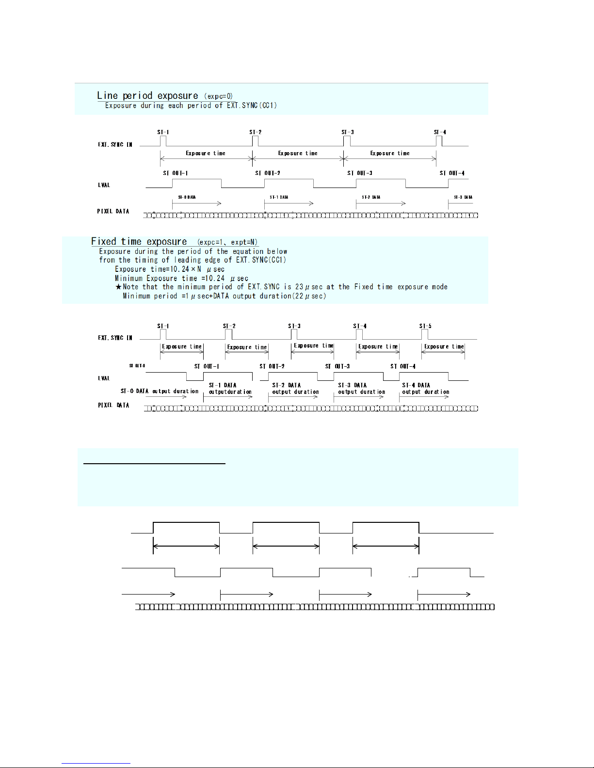
(3) Exposure control system switching (Refer to the time chart on P.11)
Line period exposure Exposure during periodic time
Fixed time exposure Exposure during pre-set time
Pulse width exposure Exposure during the pulse width of EXT.SYNC
(4) GAIN switching
Selection of GAIN position 1,2,3,…………8 ×
Selection of GAIN position for each channel ODD/EVEN adjustment
(5) Adjustment of OFFSET
OFFSET adjustment for each channel (ODD/EVEN)
T
-
2
0
TL-1024UCL
TL-2048UCL
TL-4096UCL
TL-7400UCL
TL-7400RCL
TL-7450UCL
Page 8

8 / 17
[Network transmission setting]
Baud rate :9600bps
Data Length :8bit
Start Bit :1bit
Stop Bit :1bit
Parity :Non
Xon / Xoff Control :Non
[Communication overall]
1. Viewing
To view the status of the camera.
e.g. Id? <CR> To view the camera ID.
2. Setting
To set the status of the camera.
e.g. sync=1 <CR> To set SYNC system to EXT.SYNC
[Glossary]
[ ] ……omissible
<CR> ……carriage return
N ……arbitrary numeral indicating some value
A ……arbitrary numeral indicating GAIN position
X ……arbitrary numeral indicating channel
Gain position……GAIN position of the camera
Channel …….Channel to specify the GAIN control device for each CCD output line
EEPROM …….EEPROM incorporated in the camera
[Notes]
・Command name must be lower-case. Upper-case character is not valid.
・Input character must be one-byte character. Double-byte character is not valid.
・Blank is not valid.
・Line feed code is indicated by “CR(0x0D)”. And also “LF(0×0A)” and “CR+LF” are usable.
However returning line feed code must be CR only.
<When in use of Hyper terminal>
・Retyping is required in case of inputting error .(Correction by cursor movement is not valid.)
Page 9

9 / 17
[ Description of exceptional case]
*NG is returned when in command input error or in inputting nonexistent command.
e.g. : Command input error (Gain position No. is not designated. )
Input: ch1gain=96
Output: NG
e.g. : Input of nonexistent command
Input: chake
Output: NG
*NE is returned when in numeric entry error.
e.g. : Input error (Input value is beyond the setting range.)
Input: gainpos=96
Output: NE
e.g. : Input error (Input value is beyond the setting range.)
Input: ch1gain1=2000
Output: NE
*NC is returned when in inputting invalid value under the condition that the ctrl setting (DIP-SW setting) is 0.
e.g. :
Input: ch1gain=9 (at ctrl=0)
Output: NC
*TO is returned when a command input period overruns the time-out period (15 sec.).
e.g. :
Input: gainpo (No CR entry)
Output: TO
*” ? ” at the bottom of Command is omissible
e.g. :
Input: id
Output: 0
Page 10

10 / 17
【Command Protocol】(PC->Camera)
No.
Command
Name
Format Argument Return value Explanantion
Communication
1 Check check<CR> Non OK Command for communication test
Camera setting
2 Ctrl (view) ctrl[?]<CR> Non
0:Dip Switch
1:Com
View the effective state of Communication setting value/DIP
SW.
3 Ctrl (set) ctrl=N<CR>
N=0:Dip Sw
N=1:Com
OK
Set the effective state of Communication setting value/DIP
SW.
4
Dip Sw (view) dipsw<CR> Non 0~255
View the state of DIP SW
Return the state of DIP SW in decimal number
User ID
5 ID (view) id[?]<CR> Non ID(default:0)
View the camera ID.
Administrative use for plural cameras.
For user's operation.
6 ID (set) id=N<CR> N:0~255 OK
Set the camera ID.
Administrative use for plural cameras.
For user's operation.
Output bit
7
Output bit
(view)
bit[?]<CR> Non
8: 8bit(default)
10: 10bit
View the output bit format of the camera.
8
Output bit
(set)
bit=N<CR>
N= 8 : 8bit
N=10 : 10bit
OK
Set the output bit format of the camera.
*Settable only at ctrl=1.
SYNC switching
9
Sync (view). sync[?]<CR> Non
0:Auto
1:Ext Sync
2:Int Sync
3.ExtSync &
Anti Blooming
View the state of SYNC mode.
*Effective value only at ctrl=1.
10
Sync (set) sync=N<CR>
0:Auto
1:Ext Sync
2:Int Sync
3.ExtSync &
Anti Blooming
OK
Set the SYNC mode.
*Settable only at ctrl=1.
Exposure control
11
Exposure
control
expc[?]<CR> Non
0:Line period exposure
1:Fixed time exposure
2:Pulse width exposure
View the exposure control state of the camera.
*Effective value only at ctrl=1.
12
Exposure
control
(set)
expc=N<CR>
0:Line period exposure
1:Fixed time exposure
2:Pulse width exposure
OK
Set the exposure control state of the camera.
*Settable only at ctrl=1.
Exposure time
13
Exposure
time
expt[?]<CR> Non
0~255:Exposure time
View the period at Fixed time exposure mode.
*Effective value only at ctrl=1
14
Exposure
time
expt=N<CR> N=0~255:Exposure time OK
Set the period at Fixed time exposure mode.
*Settable only at ctrl=1
Gain
15
Gain Position
(view)
gainpos[?]<CR> Non 1~8:gain position
View the Gain position of the camera.
*Effective value only at ctrl=1
16
Gain Position
(set)
gainpos=A<CR> A=1~8:gain position OK
Set the Gain position of the camera.
*Settable only at ctrl=1
17
chXgainA
(view)
chXgainA[?]<CR>
X=1~2:ch
A=1~8:gain position
0~255:gain level
View the Gain value fow each Gain position of each channel.
18
chXgainA
(set)
chXgainA=N<CR>
X=1~2:ch
A=1~8:gain position
N=0~255:gain level
OK
Set the Gain value fow each Gain position of each channel.
*Settable only at ctrl=1
Offset
19
chXoffset
(view)
chXoffset[?]<CR> X=1~2:ch 0~31:offset level View the offset value of each channel.
20
chXoffset
(set)
chXoffset=N<CR>
X=1~2:ch
N=0~31:offset level
OK
Set the offset value of each channel.
*Settable only at ctrl=1
EEPROM
21
Save save<CR> Non OK Save the setting to EEPROM.
22
Load load<CR> Non OK Load the setting from EEPROM.
System
23
Version ver<CR> Non Version View the version of microcomputer control program of the camera.
24
Revision rev<CR> Non Revision View the version of EPGA.
25
Initialize init<CR> Non OK Load the factory default.
26
config cfg<CR> Non (data output) View the all current setting data of the camera.
Page 11
11 / 17
9. Exposure control
EXT.SYNC IN
LVAL
PIXEL DATA
ST-1
Exposure tim e
ST-1 DATA outpu t duration
ST-2
ST-2 DATA outpu t duration
ST OUT-1 ST OUT-2
ST-3
ST-0 DA TA output duratio n
ST OUT-0
ST-3 DATA output duration
ST OUT-2
Exposur e time
Exposur e time
Pulse width exposure (expc=2)
Exposure during the period of the pulse width(H) of EXT.SYNC(CC1
Minimum exposure time =10.24μsec
★Note that the minimum period of EXT.SYNC is 23μsec at the Pulse width exposure mode
Minimum period = 1μsec + DATA output duration(22μsec)
Page 12

12 / 17
10. Setup steps of Hyper terminal.
[Setup of Hyper terminal ]
1) Select “Start”→ “Programs”→”Accessories”→”Communications”→”Hyper Terminal”
2) The windows will appear with the picture below.
3) When the next picture appears, enter any name.(e.g. GMA_RS232C)
Then click the “OK” button.
4) When the next picture appears, select “ COM? ” on Connect using.
(? changes depending on the setting of the computer. )
Then click the “OK” button.
Page 13

13 / 17
5) When the next picture appears, select each items as follows.(9600,8,None,1,Non)
Then click the “OK” button.
[Communication settings]
Baud Rate : 9600bps
Data Length : 8bit
Start Bit : 1bit
Stop Bit : 1bit
Parity : Non
Xon/Xoff Control : Non
6) The next picture will appear.
7) Select [File]→ [Properties]
Page 14
14 / 17
8) When the next picture appears, select “Settings” tag.
9) When the next picture appears, click the “ASCII Setup” button.
10) When the next picture appears, select each items as follows.(☑, ☑, 0, 0,☑, blank, blank)
Then click the “OK” button.
11) The screen display will return to the screen of 9).
Then click the OK button.
Page 15

15 / 17
12) End of setup.
Confirm the connection of the camera ,
enter “check” on the screen below
and then send it out.
If “OK” is displayed on the screen, communication processing has been completed.
13) Select “Start”→ “Programs”→”Accessories”→”Communications”→”Hyper Terminal” →”(*1) ”, when to launch
the Hyper terminal again with the same settings after having exited the above screen.
*1………The name which was entered at section 3)
Page 16

16 / 17
11. Notes
Precautions for use
■ Do not make an impact on the equipment.
■ Do not lag the equipment with heat insulating agent. If the equipment is covered with heat insulating agent, It
produces an increase in temperature and it causes the equipment to malfunction.(except for low-temperature
environment use)
■ Take appropriate measures such as heat removal or cold removal to prevent dew condensation, when to move It
to the place where temperature difference is extremely severe. Usage with dew condensation causes the
equipment to malfunction.
■ When the equipment is not used for a long time, protect the imaging device from dust or scratch by attaching a
lens cap. Do not store the equipment at the following places.
・The place where is subjected to a lot of dust and moisture.
・The place where is subjected to direct sunlight.
・The place where is extremely hot or cold.
・The place in the vicinity of an object which generates intensive electromagnetic field.
・The place where is subjected to intensive vibration.
■ Please wipe off the dirt on the lens surface with a cotton swab preventing scratch to the lens surface.
Use a soft cloth to clean up the camera body.
■ Use the equipment with a voltage within the range of specifications and do not connect the equipment to a power
source that contains intense noise components. In such case, the image output from the camera may contains
noise components.
■ Do not use the equipment in an environment subject to intense electromagnetic field.
In such an environment, malfunction of the camera, disturbance of image and noise are caused by the field.
■ In case of the high-intensity object, it may happen that even the low intensity part is displayed whitely like a
vertical streak above and below the high-intensity object. This phenomenon is called “smear”. However it is the
problem specific to CCD and it is not the camera-related failure.
■ In case of the linear object, jagged picture may be displayed. Also in case of the pinstripe or checkered pattern,
annual rings- like picture may be displayed. However these are also the problem specific to CCD and it is not the
camera-related failure.
■ The lighting using a commercial power source may cause a perceptible flicker at higher shutter speed.
In cases like this, consider to adjust shutter speed setting of the camera or to use the DC lighting or high-
frequency lighting.
Attention
■ All rights on this manual reserved.
■ The specifications and operational details described in the manual are subject to change for performance
improvement or other reasons without notice.
Page 17

17 / 17
12. External dimensions
Element
6
18
8 0.3
63.5
63.58
3 1.3 1 7.5 17.5
6 45 .4
18
4-M2.6
F. B:4 6. 5
F -
Mount
Ca mera L ink
P O W E R
MADEIN JAPAN
1/4-20U NC Depth8
2-M6 Depth8
SER.NO.
MODEL
TL-
51 50
UCL
(20.2)
Φ 64.3
M 2.6 Depth 6
( Four faces)
 Loading...