

TSM1N60L
600V N-Channel Power MOSFET
1/7 Version: A07
TO-252
TO-251
General Description
The TSM1N60L is used an advanced termination scheme to provide enhanced voltage-blocking capability without
degrading performance over time. In addition, this advanced MOSFET is designed to withstand high energy in
avalanche and commutation modes. The new energy efficient design also offers a drain- to-source diode with a fast
recovery time. Designed for high voltage, high speed switching applications in power supplies, converters and PWM
motor controls, these devices are particularly well suited for bridge circuits where diode speed and commutating safe
operating areas are critical and offer additional and safety margin against unexpected voltage transients.
Features
● Robust high voltage termination
● Avalanche energy specified
● Diode is characterized for use in bridge circuits
● Source to Drain diode recovery time comparable to a
discrete fast recovery diode.
● I
DSS
and V
DS(on)
specified at elevated temperature
Ordering Information
Part No.
Package
Packing
TSM1N60LCP RO
TO-252
2.5Kpcs / 13” Reel
TSM1N60LCH C5
TO-251
50pcs / Tube
Absolute Maximum Rating (Ta = 25
o
C unless otherwise noted)
Parameter
Symbol
Limit
Unit
Drain-Source Voltage
VDS
600
V
Gate-Source Voltage
VGS
±30
V
Continuous Drain Current
ID 1 A
Pulsed Drain Current
IDM 4 A
Continuous Source Current (Diode Conduction)
a,b
IS 1 A
Single Pulse Drain to Source Avalanche Energy
(VDD = 100V, VGS=10V, IAS=2A, L=10mH, RG=25Ω)
EAS
20
mJ
Maximum Power Dissipation @Ta = 25 oC
PD
2.5
W
Operating Junction Temperature
TJ
+150
o
C
Operating Junction and Storage Temperature Range
TJ, T
STG
-55 to +150
o
C
PRODUCT SUMMARY
VDS (V)
R
DS(on)
(Ω)
ID (A)
600
12 @ V
GS
=10V
1
Pin Definition:
1. Gate
2. Drain
3. Source
Block Diagram
N-Channel MOSFET
TSM1N60L
600V N-Channel Power MOSFET
2/7 Version: A07
Thermal Performance
Parameter
Symbol
Limit
Unit
Lead Temperature (1/8” from case)
TL
10
S
Thermal Resistance - Junction to Ambient
RӨJA
62.5
o
C/W
Notes: Surface mounted on FR4 board t ≤ 10sec
Electrical Specifications (Ta = 25
o
C unless otherwise noted)
Parameter
Conditions
Symbol
Min
Typ
Max
Unit
Static
Drain-Source Breakdown Voltage
V
GS
= 0V, ID = 250uA
BV
DSS
600
--
--
V
Drain-Source On-State Resistance
V
GS
= 10V, ID = 0.6A
R
DS(ON)
--
10.5
12
Ω
Gate Threshold Voltage
V
DS
= VGS, ID = 250uA
V
GS(TH)
2.0
--
4.0
V
Zero Gate Voltage Drain Current
V
DS
= 600V, VGS = 0V
I
DSS
--
--
10
uA
Gate Body Leakage
VGS = ±20V, VDS = 0V
I
GSS
--
--
± 100
nA
Forward Transconductance
V
DS
≧50V, ID = 0.5A
gfs
--
10
--
S
Diode Forward Voltage
IS = 1A, VGS = 0V
VSD
--
--
1.5
V
Dynamic b
Total Gate Charge
Qg
--
8.5
14
Gate-Source Charge
Qgs
--
1.8
--
Gate-Drain Charge
V
DS
= 400V, ID = 1A,
V
GS
= 10V
Qgd
-- 4 --
nC
Input Capacitance
C
iss
--
210
--
Output Capacitance
C
oss
--
28
--
Reverse Transfer Capacitance
V
DS
= 25V, VGS = 0V,
f = 1.0MHz
C
rss
--
4.2
--
pF
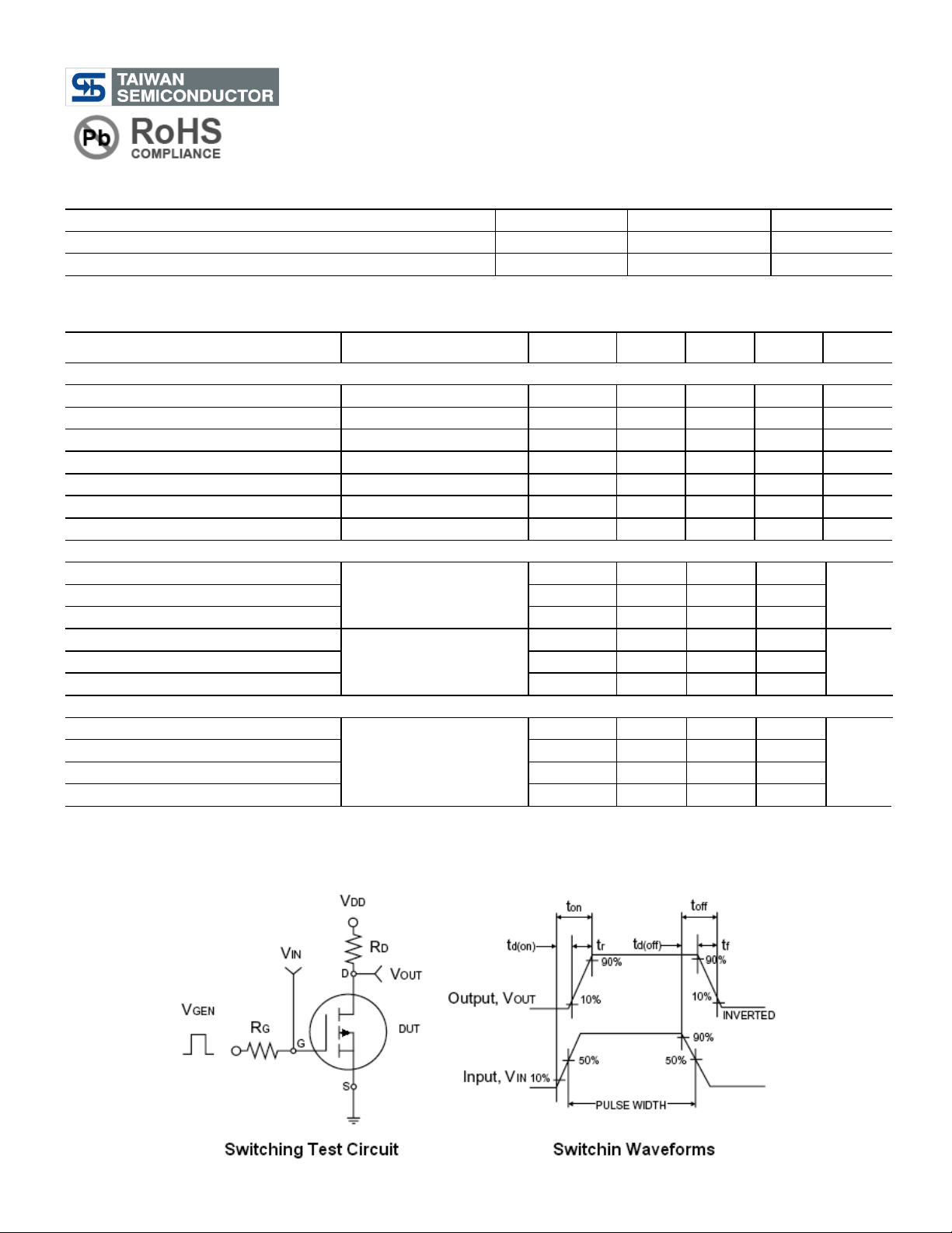
Switching c
Turn-On Delay Time
t
d(on)
-- 8 --
Turn-On Rise Time
tr
--
21
--
Turn-Off Delay Time
t
d(off)
--
18
--
Turn-Off Fall Time
V
GS
= 10V, ID = 1A,
V
DS
= 300V, RG = 6Ω
tf
--
24
--
nS
Notes:
a. Pulse test: pulse width <=300uS, duty cycle <=2%
b. For design reference only, not subject to production testing.
c. Switching time is essentially independent of operating temperature.
TSM1N60L
600V N-Channel Power MOSFET
3/7 Version: A07
Electrical Characteristics Curve (Ta = 25
o
C, unless otherwise noted)
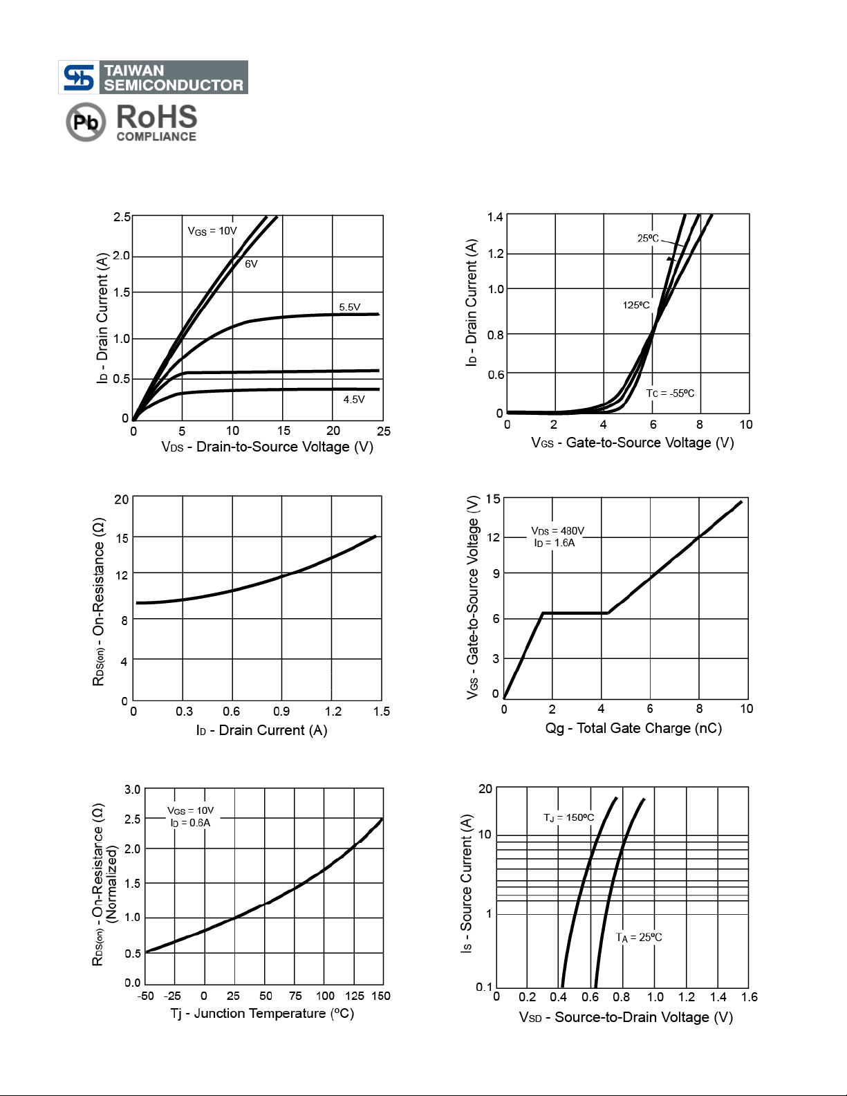
Output Characteristics
Transfer Characteristics
On-Resistance vs. Drain Current
Gate Charge
On-Resistance vs. Junction Temperature
Source-Drain Diode Forward Voltage

TSM1N60L
600V N-Channel Power MOSFET
4/7 Version: A07
Electrical Characteristics Curve (Ta = 25
o
C, unless otherwise noted)
On-Resistance vs. Gate-Source Voltage
Threshold Voltage
Maximum Safe Operating Area
Normalized Thermal Transient Impedance, Junction-to-Ambient

TSM1N60L
600V N-Channel Power MOSFET
5/7 Version: A07
SOT-252 Mechanical Drawing
Marking Diagram
Y
= Year Code
M
= Month Code
(A=Jan, B=Feb, C=Mar, D=Apl, E=May, F=Jun, G=Jul, H=Aug,
I=Sep, J=Oct, K=Nov, L=Dec)
L
= Lot Code
TO-252 DIMENSION
MILLIMETERS
INCHES
DIM
MIN
MAX
MIN
MAX
A
2.3BSC
0.09BSC
A1
4.6BSC
0.18BSC
B
6.80
7.20
0.268
0.283
C
5.40
5.60
0.213
0.220
D
6.40
6.65
0.252
0.262
E
2.20
2.40
0.087
0.094
F
0.00
0.20
0.000
0.008
G
5.20
5.40
0.205
0.213
G1
0.75
0.85
0.030
0.033
G2
0.55
0.65
0.022
0.026
H
0.35
0.65
0.014
0.026
I
0.90
1.50
0.035
0.059
J
2.20
2.80
0.087
0.110
K
0.50
1.10
0.020
0.043
L
0.90
1.50
0.035
0.059
M
1.30
1.70
0.051
0.67

TSM1N60L
600V N-Channel Power MOSFET
6/7 Version: A07
SOT-251 Mechanical Drawing
Marking Diagram
Y
= Year Code
M
= Month Code
(A=Jan, B=Feb, C=Mar, D=Apl, E=May, F=Jun, G=Jul, H=Aug,
I=Sep, J=Oct, K=Nov, L=Dec)
L
= Lot Code
TO-251 DIMENSION
MILLIMETERS
INCHES
DIM
MIN
MAX
MIN
MAX
A
2.20
2.4
0.087
0.095
A1
1.10
1.30
0.043
0.051
b
0.40
0.80
0.016
0.032
C
0.40
0.60
0.016
0.024
D
6.70
7.30
0.264
0.287
D1
5.40
5.65
0.213
0.222
E
6.40
6.65
0.252
0.262
e
2.10
2.50
0.083
0.098
F
0.40
0.60
0.016
0.024
L
7.00
8.00
0.276
0.315
L1
1.60
1.86
0.063
0.073

TSM1N60L
600V N-Channel Power MOSFET
7/7 Version: A07
Notice
Specifications of the products displayed herein are subject to change without notice. TSC or anyone on its behalf,
assumes no responsibility or liability for any errors or inaccuracies.
Information contained herein is intended to provide a product description only. No license, express or implied, to any
intellectual property rights is granted by this document. Except as provided in TSC’s terms and conditions of sale for
such products, TSC assumes no liability whatsoever, and disclaims any express or implied warranty, relating to sale
and/or use of TSC products including liability or warranties relating to fitness for a particular purpose, merchantability,
or infringement of any patent, copyright, or other intellectual property right.
The products shown herein are not designed for use in medical, life-saving, or life-sustaining applications. Customers
using or selling these products for use in such applications do so at their own risk and agree to fully indemnify TSC for
any damages resulting from such improper use or sale.
 Loading...