TAIWAN SEMICONDUCTOR TS321 Operation Manual

TS321
Low Power Single Operational Amplifier
1/6 Version: A07
SOT-25
General Description
The TS321 brings performance and economy to low power systems. With high unity gain frequency and a guaranteed
0.4V/uS slew rate, the quiescent current is only 430uA/amplifier (5V). The input common mode range includes ground
and therefore the device is able to operate in single supply applications as well as in dual supply applications. It is also
capable of comfortably driving large capacitive loads.
The TS321 is available in the SOT-25 package. Overall the TS321 is a low power, wide supply range performance OP
Amp that can be designed into a wide range of applications at an economical price without sacrificing valuable board
space.
Absolute Maximum Rating
Parameter
Symbol
Limit
Unit
Supply Voltage
Vcc
+32
V
Input Voltage
VIN
-0.3 to +32
V
Input Current (VIN < -0.3V)
VI
50
mA
Output Short Circuit Duration
tsc
Continuous
Operating Temperature Range
T
OPR
-40 ~ +85
o
C
Storage Temperature Range
T
STG
-65 ~ +150
o
C
Mounting Temperature (Soldering @ 260 oC)
10
S
Thermal Resistance Junction to Ambient
RӨJA
265
o
C/W
Features
● Short circuit protected outputs
● True differential input stage
● Wide supply voltage range +3V to 32V
● Low input bias currents
● Internally compensated
● Common mode range extends to negative supply
● Single Version of TS324
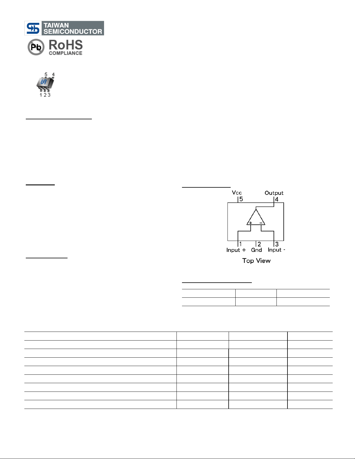
Block Diagram
Applications
● Chargers
● Power Supplies
● Industrial: Controls, Instruments
● Desktops
● Communications Infrastructure
Ordering Information
Part No.
Package
Packing
TS321CX5 RF
SOT-25
3Kpcs / 7” Reel
Pin Definition:
1. Input +
2. Ground
3. Input -
4. Output
5. Vcc

TS321
Low Power Single Operational Amplifier
2/6 Version: A07
Electrical Characteristics Unless otherwise specified, all limits guarantee for at T
A
=25ºC, V+=5V, V-=5V,
Vo=1.4V. Boldface limits apply at temperature extremes.
Symbol
Parameter
Conditions
Min
Typ
Max
Units
VOS
Input Offset Voltage
(Note 1)
--
-- 2 -- 7 9
mV
IOS
Input Offset Current
--
-- 5 --
50
150
nA
IB
Input Bias Current (Note 8)
--
--
45
--
250
500
nA
VCM
Input Common-Mode Voltage Range
V+ = 30V (Note 9)
For CMRR > = 50dB
0
--
--
--
V+ -1.5
V+ -2
V
AV
Large Signal Voltage Gain
(V+ = 15V, RL =2kΩ
Vo = 1.4V to 11.4V)
25
15
100
--
--
--
V/mV
PSRR
Power Supply Rejection Ratio
RS ≤ 10kΩ, V+ ≤ 5V to 30V
65
100
--
dB
CMRR
Common Mode Rejection Ratio
RS ≤ 10kΩ
65
85
--
dB
V+ = 30V, RL =2kΩ
26
--
--
VOH
V+ = 30V, RL = 10kΩ
27
28
--
V
VO
Output Swing
VOL
V+ = 5V, RL = 10kΩ
-- 5 20
mV
V+ = 5V
--
--
0.43
0.7
1.15
1.2
IS
Supply Current, No Load
V+ = 30V
--
--
0.66
1.5
2.85
3
mA
I
SOURCE
Output Current Sourcing
VID = +1V, V+ = 15V,
VO =2V
20
10
40
20
--
--
mA
VID = −1V
V+ = 15V, VO =2V
10 5 20 8 --
--
mA
I
SINK
Output Current Sinking
VID = −1V
V+ = 15V, VO = 0.2V
--
12
--
100
--
--
µA
IO
Output Short Circuit to Ground
V+ = 15V
--
40
85
mA
SR
Slew Rate
V+ = 15V, RL =2kΩ,
VIN = 0.5 to 3V
CL = 100pF, Unity Gain
--
0.4
--
V/µs
GBW
Gain Bandwidth Product
V+ = 30V, f = 100kHz,
VIN = 10mV, RL =2kΩ,
CL = 100pF
-- 1 --
MHz
THD
Total Harmonic Distortion
f = 1kHz, AV = 20dB
RL =2kΩ, VO = 2V
PP
CL = 100pF, V+ = 30V
--
0.015
--
%
en
Equivalent Input Noise Voltage
f = 1kHz, RS = 100Ω
V+ = 30V
--
40
--
nV
Note:
1. Vo≒1.4V, Rs=0Ω with V+ from 5V to 30V; and over the full input common-mode range(0V~V+ -1.5V)at 25 oC
2. short circuits from the output V+ can cause excessive heating and eventual destruction. When considering short
circuits to ground the maximum output current is approximately 40mA independent of the magnitude of V+ values of
supply voltage in excess of +15v,continuous short circuit can exceed the power dissipation ratings and cause
eventual destruction.
 Loading...